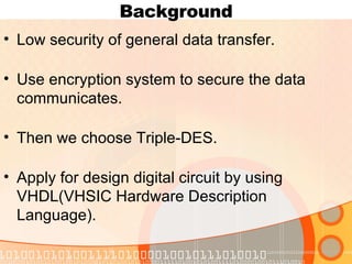
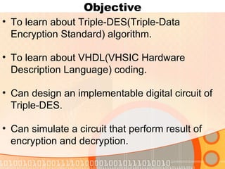
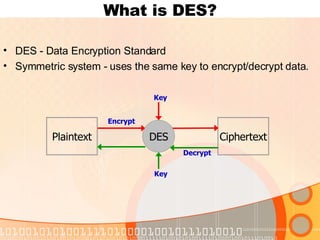
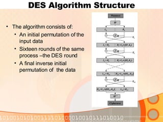
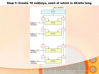
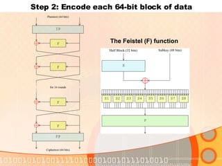
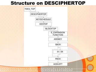
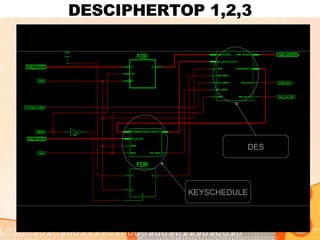
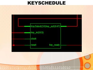
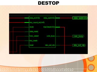
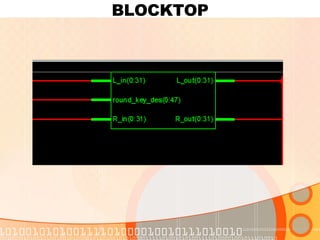
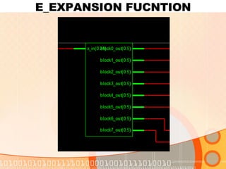
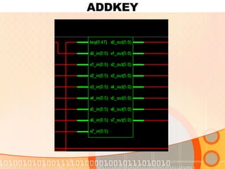
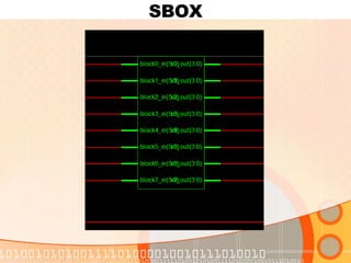
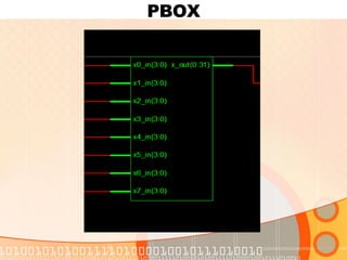
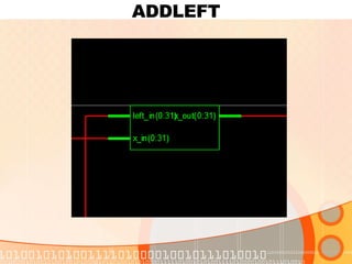
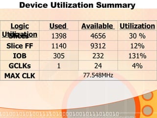
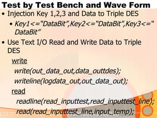
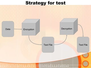
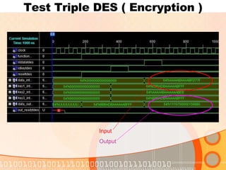
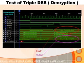
The document discusses the simulation of a Triple Data Encryption Standard (Triple DES) circuit using VHDL. It provides background on Triple DES, describes the design and structure of the Triple DES circuit in VHDL, and presents the results of testing the encryption and decryption functions of the circuit through simulation. Testing showed the circuit correctly performed encryption and decryption on input data using the Triple DES algorithm. The design utilized some FPGA resources but would require a clock generator and RAM for implementation on an actual FPGA board.
Background Low securityof general data transfer. Use encryption system to secure the data communicates. Then we choose Triple-DES. Apply for design digital circuit by using VHDL(VHSIC Hardware Description Language).
5.
Objective To learnabout Triple-DES(Triple-Data Encryption Standard) algorithm. To learn about VHDL(VHSIC Hardware Description Language) coding. Can design an implementable digital circuit of Triple-DES. Can simulate a circuit that perform result of encryption and decryption.
What is DES?DES - Data Encryption Standard Symmetric system - uses the same key to encrypt/decrypt data. Ciphertext Plaintext DES Key Key Encrypt Decrypt
9.
DES Algorithm StructureThe algorithm consists of: An initial permutation of the input data Sixteen rounds of the same process –the DES round A final inverse initial permutation of the data
10.
Step 1: Create16 subkeys, each of which is 48-bits long.
11.
Step 2: Encodeeach 64-bit block of data The Feistel ( F ) function
12.
Mode of 3DES 3 DES – EDE (2 keys 3DES) Keys = 112 bits C = E k1 ( D k2 (E k1 (M)))
13.
3DES-EDE E DE k 1 k 2 k 1 Plaintext Ciphertext D E D k 1 k 2 k 1 Ciphertext Plaintext
Coding Entity Topmodule entity test_tdestop is Port ( data_intdes : in std_logic_vector ( 0 to 63 ) ; key1_intdes : in std_logic_vector ( 0 to 63 ) ; key2_intdes : in std_logic_vector ( 0 to 63 ) ; key3_intdes : in std_logic_vector ( 0 to 63 ) ; clock : in std_logic; function_selecttdes : in std_logic; set_out : in std_logic; lddatatdes : in std_logic; ldkeytdes : in std_logic; resettdes : in std_logic; data_outtdes : out std_logic_vector ( 0 to 63 ) ; out_readytdes : out std_logic ) ;
Test by TestBench and Wave Form Injection Key 1,2,3 and Data to Triple DES Key1<=“DataBit”,Key2<=“DataBit”,Key3<=“DataBit” Use Text I/O Read and Write Data to Triple DES write write(out_data_out,data_outtdes); writeline(logdata_out,out_data_out); read readline(read_inputtest,read_inputtest_line); read(read_inputtest_line,input_temp); Test Bench not permission injection Output
Conclusion Candesign and simulation circuit . Use function for simulation circuit. Can Applied Algorithm Triple DES . Circuit has delay time and cannot control some gate. Can synthesis on FPGA board but it need clock generator and RAM. Large IOB must has floorplanning to save spaces that use.