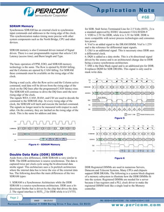
1) DDR memory technology enables memory subsystems to transfer data at twice the frequency of single data rate memory by transferring data on both the rising and falling edges of the clock. This improves performance but also makes the design and debugging more challenging due to reduced timing margins.
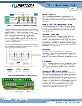
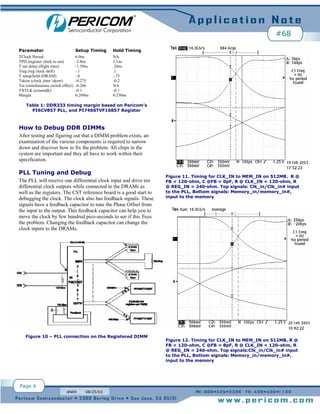
2) Debugging DDR memory modules requires examining components like the PLL to ensure proper clock generation and alignment, termination resistors to optimize timing, and registers to confirm signals are latched within specifications. Tuning elements like feedback capacitors and resistors can help optimize timing.
3) Testing tools are needed to thoroughly evaluate DDR memory, including memory testers, stress tests, and equipment to measure clock signals on DIMMs independently of a system


![Adaptive bank management[1]](https://cdn.slidesharecdn.com/ss_thumbnails/adaptivebankmanagement1-140328014749-phpapp01-thumbnail.jpg?width=640&height=640&fit=bounds)