Download to read offline
![DMOS Microstepping Driver with Translator
And Overcurrent Protection
A4988
4Allegro MicroSystems, LLC
115 Northeast Cutoff
Worcester, Massachusetts 01615-0036 U.S.A.
1.508.853.5000; www.allegromicro.com
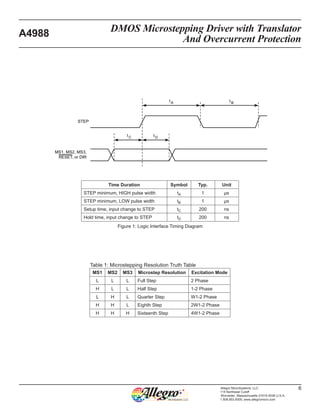
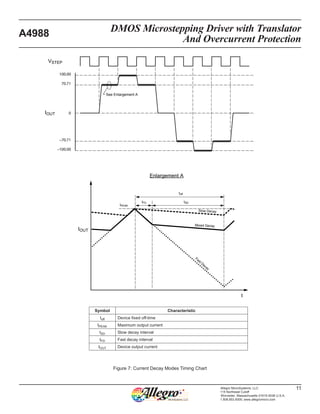
ELECTRICAL CHARACTERISTICS1 at TA = 25°C, VBB = 35 V (unless otherwise noted)
Characteristics Symbol Test Conditions Min. Typ.2 Max. Units
Output Drivers
Load Supply Voltage Range VBB Operating 8 – 35 V
Logic Supply Voltage Range VDD Operating 3.0 – 5.5 V
Output On Resistance RDSON
Source Driver, IOUT = –1.5 A – 320 430 mΩ
Sink Driver, IOUT = 1.5 A – 320 430 mΩ
Body Diode Forward Voltage VF
Source Diode, IF = –1.5 A – – 1.2 V
Sink Diode, IF = 1.5 A – – 1.2 V
Motor Supply Current IBB
fPWM < 50 kHz – – 4 mA
Operating, outputs disabled – – 2 mA
Logic Supply Current IDD
fPWM < 50 kHz – – 8 mA
Outputs off – – 5 mA
Control Logic
Logic Input Voltage
VIN(1) VDD×0.7 – – V
VIN(0) – – VDD×0.3 V
Logic Input Current
IIN(1) VIN = VDD×0.7 –20 <1.0 20 µA
IIN(0) VIN = VDD×0.3 –20 <1.0 20 µA
Microstep Select
RMS1 MS1 pin – 100 – kΩ
RMS2 MS2 pin – 50 – kΩ
RMS3 MS3 pin – 100 – kΩ
Logic Input Hysteresis VHYS(IN) As a % of VDD 5 11 19 %
Blank Time tBLANK 0.7 1 1.3 μs
Fixed Off-Time tOFF
OSC = VDD or GND 20 30 40 μs
ROSC = 25 kΩ 23 30 37 μs
Reference Input Voltage Range VREF 0 – 4 V
Reference Input Current IREF –3 0 3 μA
Current Trip-Level Error3 errI
VREF = 2 V, %ITripMAX = 38.27% – – ±15 %
VREF = 2 V, %ITripMAX = 70.71% – – ±5 %
VREF = 2 V, %ITripMAX = 100.00% – – ±5 %
Crossover Dead Time tDT 100 475 800 ns
Protection
Overcurrent Protection Threshold4 IOCPST 2.1 – – A
Thermal Shutdown Temperature TTSD – 165 – °C
Thermal Shutdown Hysteresis TTSDHYS – 15 – °C
VDD Undervoltage Lockout VDDUVLO VDD rising 2.7 2.8 2.9 V
VDD Undervoltage Hysteresis VDDUVLOHYS – 90 – mV
1For input and output current specifications, negative current is defined as coming out of (sourcing) the specified device pin.
2Typical data are for initial design estimations only, and assume optimum manufacturing and application conditions. Performance may vary for individual
units, within the specified maximum and minimum limits.
3VERR = [(VREF/8) – VSENSE] / (VREF/8).
4Overcurrent protection (OCP) is tested at TA = 25°C in a restricted range and guaranteed by characterization.](https://image.slidesharecdn.com/culwrobkr2wsn85h84ct-signature-47369da2c0af7b546eaf09641852618715999c66d4f9214bc46b19027a61ddaa-poli-201120041656/85/A4988-4-320.jpg)

![DMOS Microstepping Driver with Translator
And Overcurrent Protection
A4988
17Allegro MicroSystems, LLC
115 Northeast Cutoff
Worcester, Massachusetts 01615-0036 U.S.A.
1.508.853.5000; www.allegromicro.com
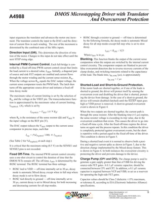
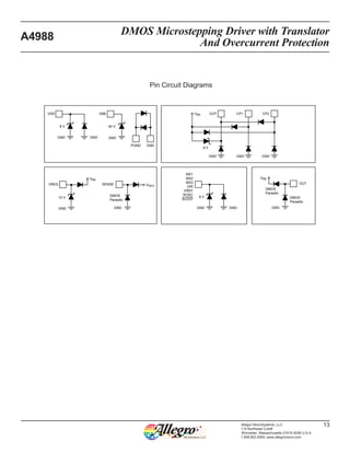
Table 2: Step Sequencing Settings
Home microstep position at Step Angle 45º; DIR = H
Full
Step
#
Half
Step
#
1/4
Step
#
1/8
Step
#
1/16
Step
#
Phase 1
Current
[% ItripMax]
(%)
Phase 2
Current
[% ItripMax]
(%)
Step
Angle
(º)
Full
Step
#
Half
Step
#
1/4
Step
#
1/8
Step
#
1/16
Step
#
Phase 1
Current
[% ItripMax]
(%)
Phase 2
Current
[% ItripMax]
(%)
Step
Angle
(º)
1 1 1 1 100.00 0.00 0.0 5 9 17 33 –100.00 0.00 180.0
2 99.52 9.80 5.6 34 –99.52 –9.80 185.6
2 3 98.08 19.51 11.3 18 35 –98.08 –19.51 191.3
4 95.69 29.03 16.9 36 –95.69 –29.03 196.9
2 3 5 92.39 38.27 22.5 10 19 37 –92.39 –38.27 202.5
6 88.19 47.14 28.1 38 –88.19 –47.14 208.1
4 7 83.15 55.56 33.8 20 39 –83.15 –55.56 213.8
8 77.30 63.44 39.4 40 –77.30 –63.44 219.4
1 2 3 5 9 70.71 70.71 45.0 3 6 11 21 41 –70.71 –70.71 225.0
10 63.44 77.30 50.6 42 –63.44 –77.30 230.6
6 11 55.56 83.15 56.3 22 43 –55.56 –83.15 236.3
12 47.14 88.19 61.9 44 –47.14 –88.19 241.9
4 7 13 38.27 92.39 67.5 12 23 45 –38.27 –92.39 247.5
14 29.03 95.69 73.1 46 –29.03 –95.69 253.1
8 15 19.51 98.08 78.8 24 47 –19.51 –98.08 258.8
16 9.80 99.52 84.4 48 –9.80 –99.52 264.4
3 5 9 17 0.00 100.00 90.0 7 13 25 49 0.00 –100.00 270.0
18 –9.80 99.52 95.6 50 9.80 –99.52 275.6
10 19 –19.51 98.08 101.3 26 51 19.51 –98.08 281.3
20 –29.03 95.69 106.9 52 29.03 –95.69 286.9
6 11 21 –38.27 92.39 112.5 14 27 53 38.27 –92.39 292.5
22 –47.14 88.19 118.1 54 47.14 –88.19 298.1
12 23 –55.56 83.15 123.8 28 55 55.56 –83.15 303.8
24 –63.44 77.30 129.4 56 63.44 –77.30 309.4
2 4 7 13 25 –70.71 70.71 135.0 4 8 15 29 57 70.71 –70.71 315.0
26 –77.30 63.44 140.6 58 77.30 –63.44 320.6
14 27 –83.15 55.56 146.3 30 59 83.15 –55.56 326.3
28 –88.19 47.14 151.9 60 88.19 –47.14 331.9
8 15 29 –92.39 38.27 157.5 16 31 61 92.39 –38.27 337.5
30 –95.69 29.03 163.1 62 95.69 –29.03 343.1
16 31 –98.08 19.51 168.8 32 63 98.08 –19.51 348.8
32 –99.52 9.80 174.4 64 99.52 –9.80 354.4](https://image.slidesharecdn.com/culwrobkr2wsn85h84ct-signature-47369da2c0af7b546eaf09641852618715999c66d4f9214bc46b19027a61ddaa-poli-201120041656/85/A4988-17-320.jpg)

This document summarizes the features and operation of the A4988 microstepping motor driver IC. It has built-in current regulation and motor control logic to drive bipolar stepper motors in various microstep modes. Key features include mixed and slow current decay modes for reduced noise and accurate stepping, internal protection from overcurrent and thermal issues, and a simple interface requiring only a STEP input to drive the motor. It operates from a single power supply and comes in a small QFN package well-suited for motor driver applications.


