Future Traffic Solution (FTS) is a proposed system using RFID and GSM technologies to help control traffic problems and reduce corruption. The system would extract vehicle registration details wirelessly using GSM to help traffic police issue fines on the spot for red light violations. It would also send violation messages to vehicle owners and help trace lost vehicles. This could increase government revenue and help traffic authorities better control traffic without issues like bribery.


![7
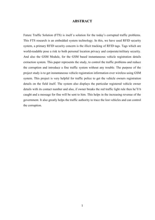
they can be used for two different functions. The first one is to perform input/output operations and the second one is used to implement special features of the microcontroller like counting external pulses, interrupting the execution of the program according to external events, performing serial data transfer or connecting the chip to a computer to update the software. Each port has 8 pins, and will be treated from the software point of view as an 8-bit variable called 'register', each bit being connected to a different Input/output pin. There are two different memory types: RAM and EEPROM. Shortly, RAM is used to store variable during program execution, while the EEPROM memory is used to store the program itself, that's why it is often referred to as the 'program memory'. It is clear that the CPU (Central Processing Unit) is the heart of the micro controllers. It is the CPU that will Read the program from the FLASH memory and execute it by interacting with the different peripherals. Diagram below shows the pin configuration of the 89S52, where the function of each pin is written next to it, and, if it exists, the dual function is written between brackets. Note that the pins that have dual functions can still be used normally as an input/output pin. Unless the program uses their dual functions, all the 32 I/O pins of the microcontroller are configured as input/output pins [1, 2, 3].
2.1.1 FEATURES:
i) Compatible with MCS-51® Products
ii) 8K Bytes of In-System Programmable (ISP) Flash Memory
– Endurance: 1000 Write/Erase Cycles
iii) 4.0V to 5.5V Operating Range
iv) Fully Static Operation: 0 Hz to 33 MHz
v) Three-level Program Memory Lock
vi) 256 x 8-bit Internal RAM
vii) 32 Programmable I/O Lines
viii) Three 16-bit Timer/Counters
ix) Eight Interrupt Sources
x) Full Duplex UART Serial Channel
xi) Low-power Idle and Power-down Modes
xii) Interrupt Recovery from Power-down Mode](https://image.slidesharecdn.com/chapter1-141107035712-conversion-gate01/85/Chapter-1-7-320.jpg)


![11
thickness than that in the voltage-off state. Because of this, these devices are usually operated between crossed polarisers such that they appear bright with no voltage (the eye is much more sensitive to variations in the dark state than the bright state). These devices can also be operated between parallel polarisers, in which case the bright and dark states are reversed. The voltage-off dark state in this configuration appears blotchy, however, because of small variations of thickness across the device. Both the liquid crystal material and the alignment layer material contain ionic compounds. If an electric field of one particular polarity is applied for a long period of time, this ionic material is attracted to the surfaces and degrades the device performance. This is avoided either by applying an alternating current or by reversing the polarity of the electric field as the device is addressed (the response of the liquid crystal layer is identical, regardless of the polarity of the applied field).
2.2.1 INTERFACING 16×2 LCD WITH 8051:
LCD display is an inevitable part in almost all embedded projects and this is about interfacing 16×2 LCD with 8051 microcontroller. Many guys find it hard to interface LCD module with the 8051 but the fact is that if you learn it properly, it’s a very easy job and by knowing it you can easily design embedded projects like digital voltmeter / ammeter, digital clock, home automation displays, status indicator display, digital code locks, digital speedometer/ odometer, display for music players etc. Thoroughly going through this article will make you able to display any text (including the extended characters) on any part of the 16×2 display screen. In order to understand the interfacing first you have to know about the 16×2 LCD module [1].
2.2.2 16×2 LCD MODULES:
16×2 LCD module is a very common type of LCD module that is used in 8051 based embedded projects. It consists of 16 rows and 2 columns of 5×7 or 5×8 LCD dot matrices. The module are talking about here is type number JHD162A which is a very popular one. It is available in a 16 pin package with back light, contrast adjustment function and each dot matrix has 5×8 dot resolution. The pin numbers, their name and corresponding functions are shown in the table below.](https://image.slidesharecdn.com/chapter1-141107035712-conversion-gate01/85/Chapter-1-11-320.jpg)


![17
sized chips can store 38-digit numbers using 128-bit Read Only Memory (ROM). A major challenge is the attachment of the antennas, thus limiting read range to only millimetres. Potential alternatives to the radio frequencies (0.125–0.1342, 0.140–0.1485, 13.56, and 840– 960 MHz) used are seen in optical RFID (or OPID) at 333 THz (900 nm), 380 THz (788 nm), 750 THz (400 nm). The awkward antennas of RFID can be replaced with photovoltaic components and IR-LEDs on the ICs [4].
2.4 GSM:
GSM/GPRS module is used to establish communication between a computer and a GSM- GPRS system. Global System for Mobile communication (GSM) is an architecture used for mobile communication in most of the countries. Global Packet Radio Service (GPRS) is an extension of GSM that enables higher data transmission rate. GSM/GPRS module consists of a GSM/GPRS modem assembled together with power supply circuit and communication interfaces (like RS-232, USB, etc) for computer. The MODEM is the soul of such modules. Wireless MODEMs are the MODEM devices that generate, transmit or decode data from a cellular network, for establishing communication between the cellular network and the computer. These are manufactured for specific cellular network (GSM/UMTS/CDMA) or specific cellular data standard (GSM/UMTS/GPRS/EDGE/HSDPA) or technology (GPS/SIM). Wireless MODEMs like other MODEM devices use serial communication to interface with and need Hayes compatible AT commands for communication with the computer (any microprocessor or microcontroller system). GSM/GPRS MODEM is a class of wireless MODEM devices that are designed for communication of a computer with the GSM and GPRS network. It requires a SIM (Subscriber Identity Module) card just like mobile phones to activate communication with the network. Also they have IMEI (International Mobile Equipment Identity) number similar to mobile phones for their identification. A GSM/GPRS MODEM can perform the following operations:
i) Receive, send or delete SMS messages in a SIM.
ii) Read, add, search phonebook entries of the SIM.
iii) Make, Receive, or reject a voice call.](https://image.slidesharecdn.com/chapter1-141107035712-conversion-gate01/85/Chapter-1-17-320.jpg)


![20
i) BSC- The BSC provides all the control functions and physical links between the MSC and BTS. It is a high-capacity switch that provides functions such as handover, cell configuration data, and control of radio frequency (RF) power levels in base transceiver stations. A number of BSCs are served by an MSC.
ii) BTS- The BTS handles the radio interface to the mobile station. The BTS is the radio equipment (transceivers and antennas) needed to service each cell in the network. A group of BTSs are controlled by a BSC [5].
FIG. 2.5-GSM](https://image.slidesharecdn.com/chapter1-141107035712-conversion-gate01/85/Chapter-1-20-320.jpg)


![23
2.7 RESISTOR:
A resistor is a passive two terminal electrical component that implements electrical resistance as a circuit element. Resistors act to reduce current flow, and at the same time, act to lower voltage level within circuits. Resistors may have fixed resistances or variable resistances. The current through a resistor is in direct proportion to the voltage across the resistor’s terminals. This relationship is represented by ohm’s law:
“I=V/R”
Where I is the current through conductor in units of amperes, V is the potential difference measured across the conductor in units of volts, and R is the resistance of the conductor in units of ohms. There are two kinds of resistors i.e. fixed resistors and variable resistors [1].
FIG. 2.8-RESISTOR](https://image.slidesharecdn.com/chapter1-141107035712-conversion-gate01/85/Chapter-1-23-320.jpg)

![25
capacitance. Sometimes charge build-up affects the capacitor mechanically, causing its capacitance to vary. In this case, capacitance is defined in terms of incremental changes,[1]
FIG. 2.9-DIFFERENT CAPACITORS
TABLE 4-TYPES OF CAPACITORS](https://image.slidesharecdn.com/chapter1-141107035712-conversion-gate01/85/Chapter-1-25-320.jpg)


![30
FIG.2.14- LED STRUCTURE
(PN JUNCTION DEVICES AND LIGHT EMITTING DIODES BY SAFA KASAP)
LEDs are usually built on an n-type substrate, with an electrode attached to the p-type layer deposited on its surface. P-type substrates, while less common, occur as well. Many commercial LEDs, especially GaN/InGaN, also use sapphire substrate [6].](https://image.slidesharecdn.com/chapter1-141107035712-conversion-gate01/85/Chapter-1-30-320.jpg)


![46
26) Select output tag and check "create hex file" box. 27) Now when you again build your program you will see the message in output window "hex file is created". 28) In your project folder you can see the hex file with same name of your project as "test.hex". 29) This file you can directly load in 8051 target board and run the application on actual environment.
30) So here I have described the procedure to create a project in keil for 8051 micro controller. To see some sample programs for 8051 in keil just go through the link "sample programs in keil" so that you can get the idea how to write a program for 8051 in keil C[7].
4.2 SOURCE CODE:
#include <at89c51xd2.h>
#include <string.h>
#include "lcd.h"
#include "usart.h"
#include "gsm.h"
xdata unsigned char smsMessage[100];
#define irSensor P1_2
void main( void )
{
const unsigned char *myString1 = "*** WELCOME ***";
const unsigned char *myString2 = " TO ";
const unsigned char *myString3 = "GSM & RFID BASED";
const unsigned char *myString4 = "VEHICLE DETAILS ";](https://image.slidesharecdn.com/chapter1-141107035712-conversion-gate01/85/Chapter-1-46-320.jpg)
![47
const unsigned char *myString5 = " EXTRACTION ";
const unsigned char *myString6 = "FLASH THE CARD ";
const unsigned char *myString7 = " NOW ";
xdata unsigned char rfIdNumber[13];
unsigned char swNo = 0;
USART_Init_9600();
Lcd_Init();
SenStringToLcd ( 1, myString1 );
SenStringToLcd ( 2, myString2 );
DelayMs(500);
SenStringToLcd ( 1, myString3 );
DelayMs(300);
SenStringToLcd ( 1, myString4 );
SenStringToLcd ( 2, myString5 );
DelayMs(500);
SenStringToLcd ( 1, "Sending SMS " );
SenStringToLcd ( 2, "****************" );
SendSms("+919030725846", "GSM Modem Test");
DelayMs( 500 );
SenStringToLcd ( 2, "SMS Sent ......." );
DelayMs( 300 );
while(1){](https://image.slidesharecdn.com/chapter1-141107035712-conversion-gate01/85/Chapter-1-47-320.jpg)
![48
SenStringToLcd ( 1, myString6 );
SenStringToLcd ( 2, myString7 );
DelayMs(5);
strcpy( rfIdNumber, "0");
USART_Ready_To_Receive();
for( swNo = 0; swNo < 12; swNo++ ){
rfIdNumber[swNo] = USART_Read_A_Char();
}
rfIdNumber[12] = '0';
SenStringToLcd ( 2, " " );
SenStringToLcd ( 2, rfIdNumber );
DelayMs( 200 );
if( !strcmp( rfIdNumber, "260092D34D2A" ) ){
SenStringToLcd ( 1, "U R Authorised " );
SenStringToLcd ( 2, "****************" );
DelayMs( 300 );
SenStringToLcd ( 1, "Please Wait " );
SenStringToLcd ( 2, "While Processing" );
DelayMs( 300 );
SenStringToLcd ( 1, " Owner Name " );
SenStringToLcd ( 2, " Spurthi " );
DelayMs( 300 );](https://image.slidesharecdn.com/chapter1-141107035712-conversion-gate01/85/Chapter-1-48-320.jpg)


![53
REFERENCES
[1] 8051 Microcontroller and Embedded Systems, by Muhammad Ali Mazidi.
[2] http://elprojects.blogspot.in/2010/06/microcontroller-at89s52-description.html.
[3] http://www.atmel.in/Images/doc1919.pdf.
[4] Elisabeth Ilie-Zudor1, Zsolt Kemény2, Péter Egri3, László Monostori4, The RFID technology and its current applications, computer and automation research institute, hungarian academy of sciences, kende u. 13–17, 1111, budapest, department of production informatics, management and control, bme, hungary.
[5] http://web.itu.edu.tr/~pazarci/WandelGoltermann_gsm.pdf (GSM).
[6] http://www.ele.uri.edu/courses/ele432/spring08/LEDs.pdf.
[7] http://www.keil.com/product/brochures/uv4.pdf.(keil software).](https://image.slidesharecdn.com/chapter1-141107035712-conversion-gate01/85/Chapter-1-53-320.jpg)


