


![ECCN 5E002 TSPA - Technology / Software Publicly Available
CC430F613x
CC430F612x
CC430F513x
www.ti.com SLAS554G – MAY 2009 – REVISED FEBRUARY 2013
12-Bit ADC, Power Supply and Input Range Conditions
over recommended ranges of supply voltage and operating free-air temperature (unless otherwise noted) (1)
PARAMETER TEST CONDITIONS VCC MIN TYP MAX UNIT
AVCC and DVCC are connected together,
Analog supply voltage,
AVCC AVSS and DVSS are connected together, 2.2 3.6 V
Full performance
V(AVSS) = V(DVSS) = 0 V
V(Ax) Analog input voltage range (2) All ADC12 analog input pins Ax 0 AVCC V
fADC12CLK = 5.0 MHz, ADC12ON = 1, 2.2 V 125 155
Operating supply current into
IADC12_A REFON = 0, SHT0 = 0, SHT1 = 0, µA
AVCC terminal (3) 3V 150 220
ADC12DIV = 0
Only one terminal Ax can be selected at one
CI Input capacitance 2.2 V 20 25 pF
time
RI Input MUX ON resistance 0 V ≤ VAx ≤ AVCC 10 200 1900 Ω
(1) The leakage current is specified by the digital I/O input leakage.
(2) The analog input voltage range must be within the selected reference voltage range VR+ to VR– for valid conversion results. If the
reference voltage is supplied by an external source or if the internal reference voltage is used and REFOUT = 1, then decoupling
capacitors are required. See REF, External Reference and REF, Built-In Reference.
(3) The internal reference supply current is not included in current consumption parameter IADC12_A.
12-Bit ADC, Timing Parameters
over recommended ranges of supply voltage and operating free-air temperature (unless otherwise noted)
PARAMETER TEST CONDITIONS VCC MIN TYP MAX UNIT
For specified performance of ADC12 linearity
parameters using an external reference voltage or 0.45 4.8 5.0
AVCC as reference. (1)
fADC12CLK ADC conversion clock For specified performance of ADC12 linearity 2.2 V, 3 V MHz
0.45 2.4 4.0
parameters using the internal reference. (2)
For specified performance of ADC12 linearity
0.45 2.4 2.7
parameters using the internal reference. (3)
Internal ADC12
fADC12OSC ADC12DIV = 0, fADC12CLK = fADC12OSC 2.2 V, 3 V 4.2 4.8 5.4 MHz
oscillator (4)
REFON = 0, Internal oscillator,
2.2 V, 3 V 2.4 3.1
fADC12OSC = 4.2 MHz to 5.4 MHz
tCONVERT Conversion time µs
External fADC12CLK from ACLK, MCLK or SMCLK, (5)
ADC12SSEL ≠ 0
RS = 400 Ω, RI = 1000 Ω, CI = 30 pF,
tSample Sampling time 2.2 V, 3 V 1000 ns
τ = [RS + RI] × CI (6)
(1) REFOUT = 0, external reference voltage: SREF2 = 0, SREF1 = 1, SREF0 = 0. AVCC as reference voltage: SREF2 = 0, SREF1 = 0,
SREF0 = 0. The specified performance of the ADC12 linearity is ensured when using the ADC12OSC. For other clock sources, the
specified performance of the ADC12 linearity is ensured with fADC12CLK maximum of 5.0 MHz.
(2) SREF2 = 0, SREF1 = 1, SREF0 = 0, ADC12SR = 0, REFOUT = 1
(3) SREF2 = 0, SREF1 = 1, SREF0 = 0, ADC12SR = 0, REFOUT = 0. The specified performance of the ADC12 linearity is ensured when
using the ADC12OSC divided by 2.
(4) The ADC12OSC is sourced directly from MODOSC inside the UCS.
(5) 13 × ADC12DIV × 1/fADC12CLK
(6) Approximately ten Tau (τ) are needed to get an error of less than ±0.5 LSB:
tSample = ln(2n+1) x (RS + RI) × CI + 800 ns, where n = ADC resolution = 12, RS = external source resistance
Copyright © 2009–2013, Texas Instruments Incorporated Submit Documentation Feedback 65](https://image.slidesharecdn.com/cc430f6137-130406081520-phpapp01/85/Cc430f6137-65-320.jpg)


![ECCN 5E002 TSPA - Technology / Software Publicly Available
CC430F613x
CC430F612x
CC430F513x
SLAS554G – MAY 2009 – REVISED FEBRUARY 2013 www.ti.com
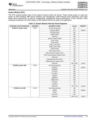
19 19
TA = 85°C TA = 85°C
TA = 25°C TA = 25°C
TA = -40°C TA = -40°C
Radio Current [mA]
Radio Current [mA]
18 18
17 17
16 16
-100 -80 -60 -40 -20 -100 -80 -60 -40 -20
Input Pow er [dBm ] Input Pow er [dBm ]
1.2 kBaud GFSK 38.4 kBaud GFSK
19 19
TA = 85°C TA = 85°C
TA = 25°C TA = 25°C
TA = -40°C TA = -40°C
Radio Current [mA]
Radio Current [mA]
18 18
17 17
16 16
-100 -80 -60 -40 -20 -100 -80 -60 -40 -20
Input Pow er [dBm ] Input Pow er [dBm ]
250 kBaud GFSK 500 kBaud MSK
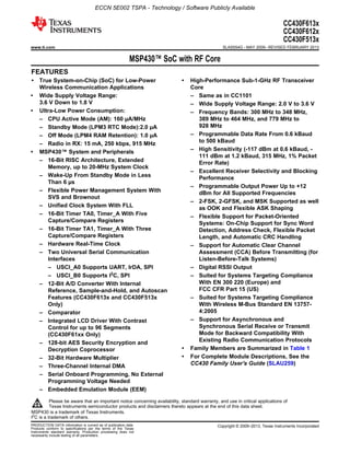
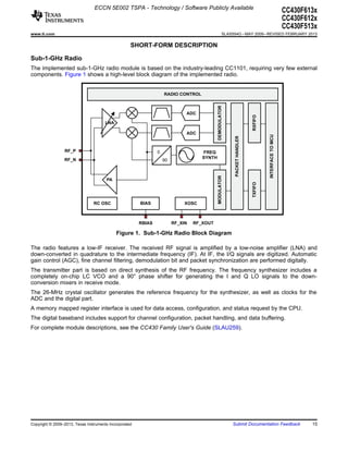
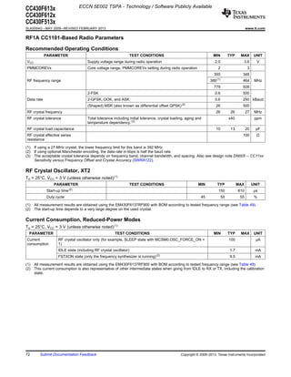
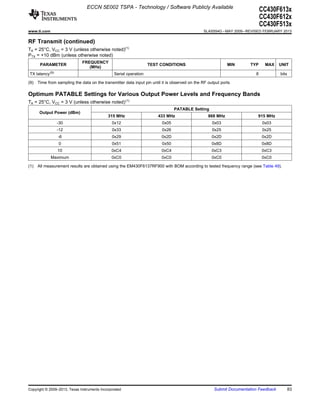
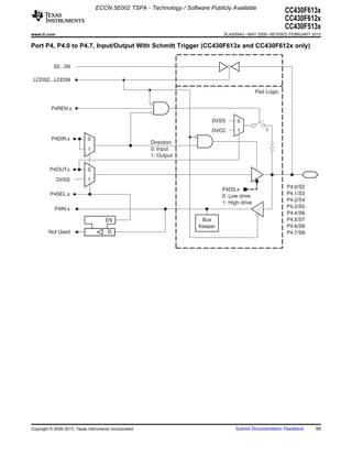
Figure 21. Typical RX Current Consumption Over Temperature and Input Power Level, 868 MHz,
Sensitivity-Optimized Setting
74 Submit Documentation Feedback Copyright © 2009–2013, Texas Instruments Incorporated](https://image.slidesharecdn.com/cc430f6137-130406081520-phpapp01/85/Cc430f6137-74-320.jpg)


![ECCN 5E002 TSPA - Technology / Software Publicly Available
CC430F613x
CC430F612x
CC430F513x
www.ti.com SLAS554G – MAY 2009 – REVISED FEBRUARY 2013
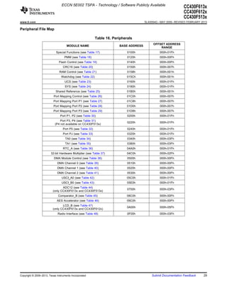
80 60
70
50
60
50 40
Selectivity [dB]
Blocking [dB]
40
30
30
20
20
10 10
0
0
-10
-20 -10
-40 -30 -20 -10 0 10 20 30 40 -1 -0.8 -0.6 -0.4 -0.2 0 0.2 0.4 0.6 0.8 1
Offset [MHz] Offset [MHz]
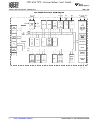
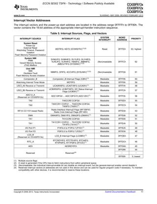
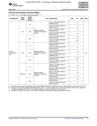
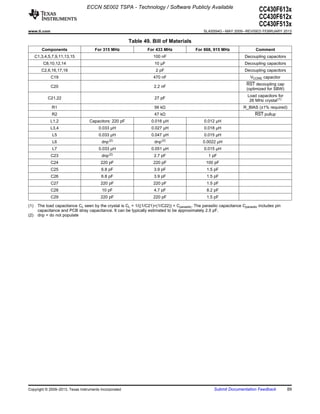
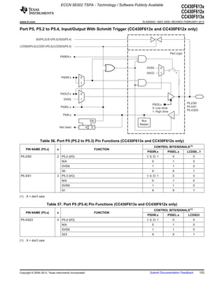
NOTE: 868.3 MHz, 2-FSK, 5.2-kHz deviation, IF frequency is 152.3 kHz, digital channel filter bandwidth is 58 kHz
Figure 22. Typical Selectivity at 1.2-kBaud Data Rate
80 50
70
40
60
50 30
Selectivity [dB]
Blocking [dB]
40
20
30
10
20
10 0
0
-10
-10
-20 -20
-40 -30 -20 -10 0 10 20 30 40 -1 -0.8 -0.6 -0.4 -0.2 0 0.2 0.4 0.6 0.8 1
Offset [MHz] Offset [MHz]
NOTE: 868 MHz, 2-FSK, 20 kHz deviation, IF frequency is 152.3 kHz, digital channel filter bandwidth is 100 kHz
Figure 23. Typical Selectivity at 38.4-kBaud Data Rate
Copyright © 2009–2013, Texas Instruments Incorporated Submit Documentation Feedback 79](https://image.slidesharecdn.com/cc430f6137-130406081520-phpapp01/85/Cc430f6137-79-320.jpg)
![ECCN 5E002 TSPA - Technology / Software Publicly Available
CC430F613x
CC430F612x
CC430F513x
SLAS554G – MAY 2009 – REVISED FEBRUARY 2013 www.ti.com
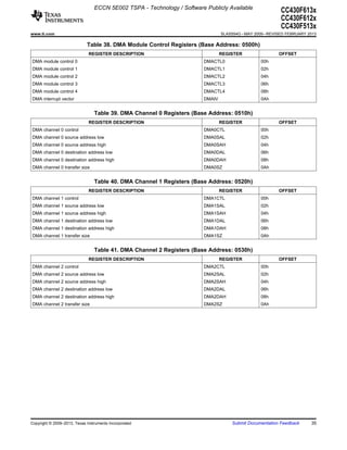
80 50
70
40
60
50 30
Selectivity [dB]
Blocking [dB]
40
20
30
10
20
10 0
0
-10
-10
-20 -20
-40 -30 -20 -10 0 10 20 30 40 -3 -2 -1 0 1 2 3
Offset [MHz] Offset [MHz]
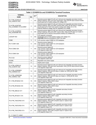
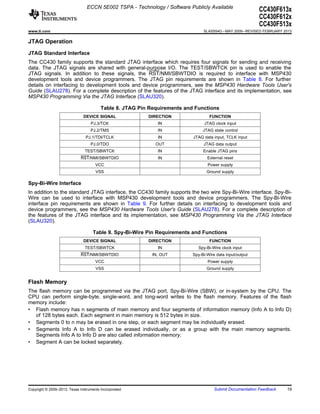
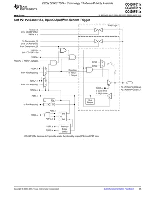
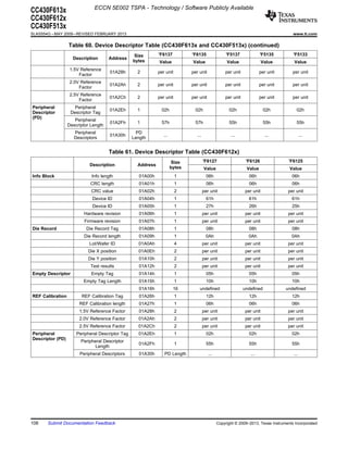
NOTE: 868 MHz, 2-FSK, IF frequency is 304 kHz, digital channel filter bandwidth is 540 kHz
Figure 24. Typical Selectivity at 250-kBaud Data Rate
80 50
70
40
60
50 30
Selectivity [dB]
Blocking [dB]
40
20
30
10
20
10 0
0
-10
-10
-20 -20
-40 -30 -20 -10 0 10 20 30 40 -3 -2 -1 0 1 2 3
Offset [MHz] Offset [MHz]
NOTE: 868 MHz, 2-FSK, IF frequency is 355 kHz, digital channel filter bandwidth is 812 kHz
Figure 25. Typical Selectivity at 500-kBaud Data Rate
80 Submit Documentation Feedback Copyright © 2009–2013, Texas Instruments Incorporated](https://image.slidesharecdn.com/cc430f6137-130406081520-phpapp01/85/Cc430f6137-80-320.jpg)


![ECCN 5E002 TSPA - Technology / Software Publicly Available
CC430F613x
CC430F612x
CC430F513x
SLAS554G – MAY 2009 – REVISED FEBRUARY 2013 www.ti.com
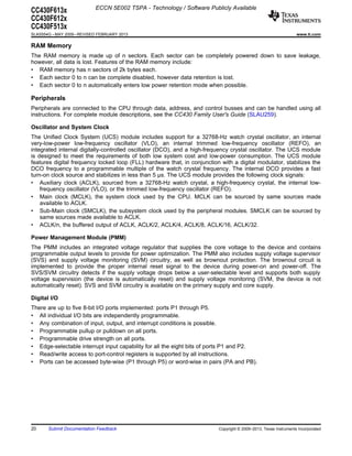
Typical RSSI_offset Values
TA = 25°C, VCC = 3 V (unless otherwise noted) (1)
RSSI_OFFSET (dB)
DATA RATE (kBaud)
433 MHz 868 MHz
1.2 74 74
38.4 74 74
250 74 74
500 74 74
(1) All measurement results are obtained using the EM430F6137RF900 with BOM according to tested frequency range (see Table 49).
0 0
1.2kBaud 250kBaud
-20 -20
500kBaud
RSSI Readout [dBm]
RSSI Readout [dBm]
38.4kBaud
-40 -40
-60 -60
-80 -80
-100 -100
-120 -120
-120 -100 -80 -60 -40 -20 0 -120 -100 -80 -60 -40 -20 0
Input Pow er [dBm ] Input Pow er [dBm ]
Figure 26. Typical RSSI Value vs Input Power Level for Different Data Rates at 868 MHz
86 Submit Documentation Feedback Copyright © 2009–2013, Texas Instruments Incorporated](https://image.slidesharecdn.com/cc430f6137-130406081520-phpapp01/85/Cc430f6137-86-320.jpg)
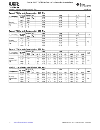
![www.ti.com
(JTAG / SBW signals)
AVDD VDD
C18
C15 R2
C13
C17
C14 C20
C12
C16
(May be added close to the respective pins
to reduce emissions at 5GHz to levels
required by ETSI.)
AVSS
AVCC
DVCC
nRST/NMI/SBWTDIO
TEST/SBWTCK
TCK
Copyright © 2009–2013, Texas Instruments Incorporated
64 63 62 61 60 59 58 57 56 55 54 53 52 51 50 49 TMS
1 48
TDI/TCLK AVDD
R1
2 47 C4
TDO
3 46
GUARD
4 45
R_BIAS C1 C2 C3
5 44
AVCC_RF
6 43 C25
SMA STRAIGHT JACK, SMT
AVCC_RF L2 L3
7 42
RF_N C27 L5 L7 C29
8 CC430F61xx 41
C23
RF_P
9 40 L1 C26
VCORE AVCC_RF
10 39
C19 VDD DVCC AVCC_RF L6 C28
documentation [MSP430 Hardware Tools User's Guide (SLAU278)].
11 38 L4
RF_XOUT C5 C6 C7
12 37
C11 C10 RF_XIN
13 36
26MHz
35
APPLICATION CIRCUIT
14 C24
15 34 C21 C22
16 33
17 18 19 20 21 22 23 24 25 26 27 28 29 30 31 32
DVCC
VDD
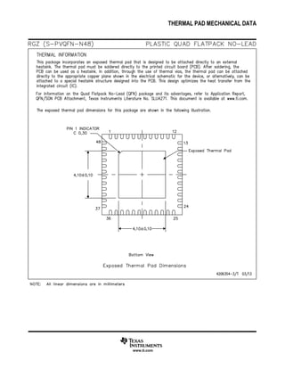
Figure 27. Typical Application Circuit CC430F61xx
C9 C8
ECCN 5E002 TSPA - Technology / Software Publicly Available
For a complete reference design including layout see the CC430 Wireless Development Tools and related
Submit Documentation Feedback
SLAS554G – MAY 2009 – REVISED FEBRUARY 2013
CC430F513x
CC430F612x
CC430F613x
87](https://image.slidesharecdn.com/cc430f6137-130406081520-phpapp01/85/Cc430f6137-87-320.jpg)
![88
CC430F513x
CC430F612x
CC430F613x
(JTAG / SBW signals)
AVDD VDD
C18
C15 R2
C13
C17
C14 C20
C12
C16
Submit Documentation Feedback
(May be added close to the respective pins
to reduce emissions at 5GHz to levels
required by ETSI.)
SLAS554G – MAY 2009 – REVISED FEBRUARY 2013
AVSS
AVCC
DVCC
nRST/NMI/SBWTDIO
TEST/SBWTCK
TCK
TMS
48 47 46 45 44 43 42 41 40 39 38 37 R1
TDI/TCLK AVDD
1 36
TDO C4
2 35
GUARD
3 34
R_BIAS C1 C2 C3
4 33
AVCC_RF
5 32 C25
SMA STRAIGHT JACK, SMT
AVCC_RF L2 L3
6 31
VCORE CC430F51xx RF_N C27 C29
7 30 L5 L7
DVCC C23
C19 VDD RF_P
8 29 L1 C26
documentation [MSP430 Hardware Tools User's Guide (SLAU278)].
AVCC_RF
9 28
C11 C10 AVCC_RF L6 C28
10 27 L4
RF_XOUT C5 C6 C7
11 26
RF_XIN
12 25
13 14 15 16 17 18 19 20 21 22 23 24 26MHz
C24
C21 C22
DVCC
VDD
C9 C8
Figure 28. Typical Application Circuit CC430F51xx
ECCN 5E002 TSPA - Technology / Software Publicly Available
For a complete reference design including layout see the CC430 Wireless Development Tools and related
www.ti.com
Copyright © 2009–2013, Texas Instruments Incorporated](https://image.slidesharecdn.com/cc430f6137-130406081520-phpapp01/85/Cc430f6137-88-320.jpg)


This document provides information on the MSP430 SoC with RF Core, which is a family of ultra-low power microcontroller system-on-chip devices with integrated sub-1GHz RF transceiver cores. The devices combine the MSP430 CPU with up to 32KB flash memory, 4KB RAM, timers, ADC, communication interfaces, security features, and an RF transceiver core. They are suited for wireless sensor applications like smart meters and thermostats requiring low power and RF connectivity. Device features and available family members are described.