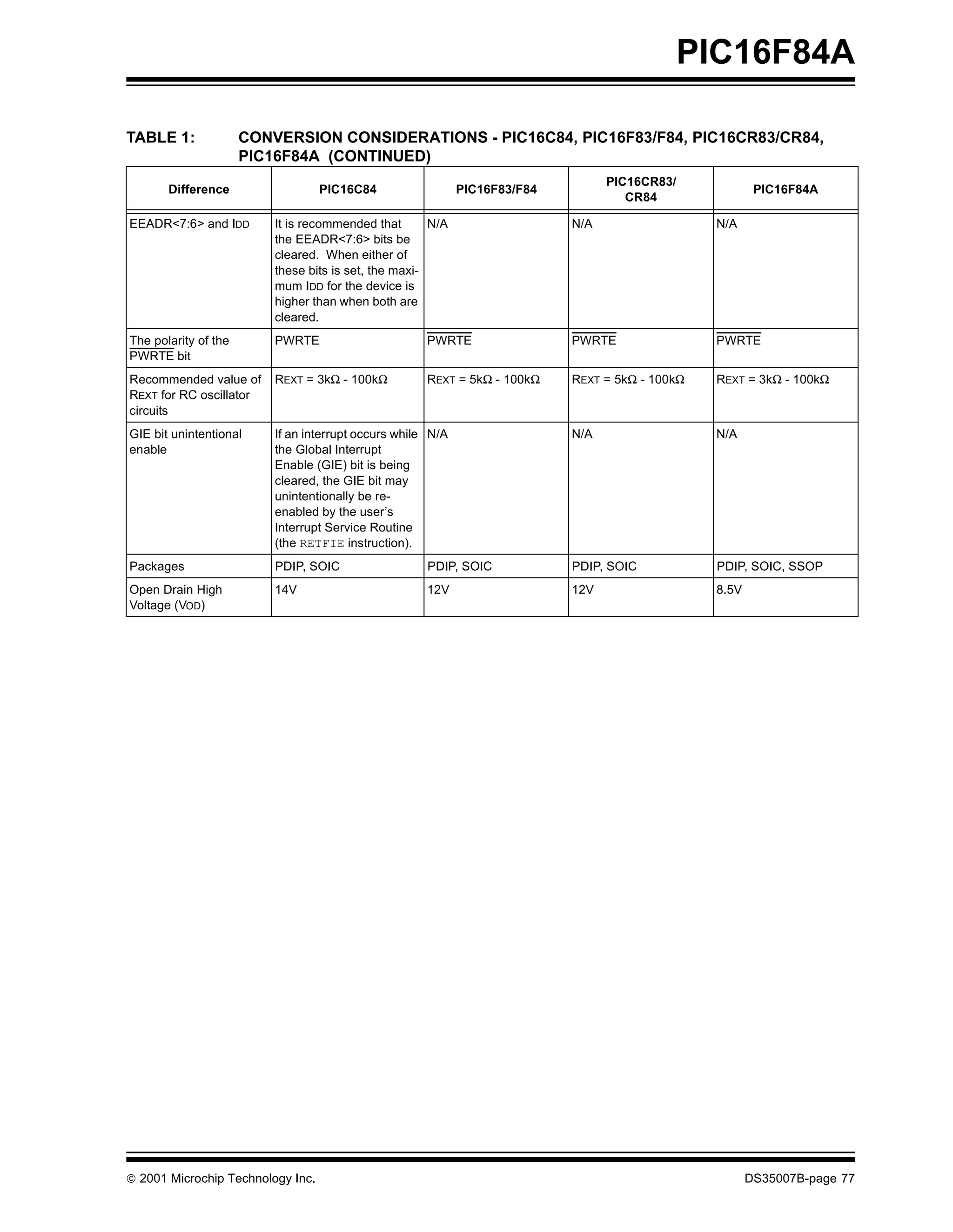
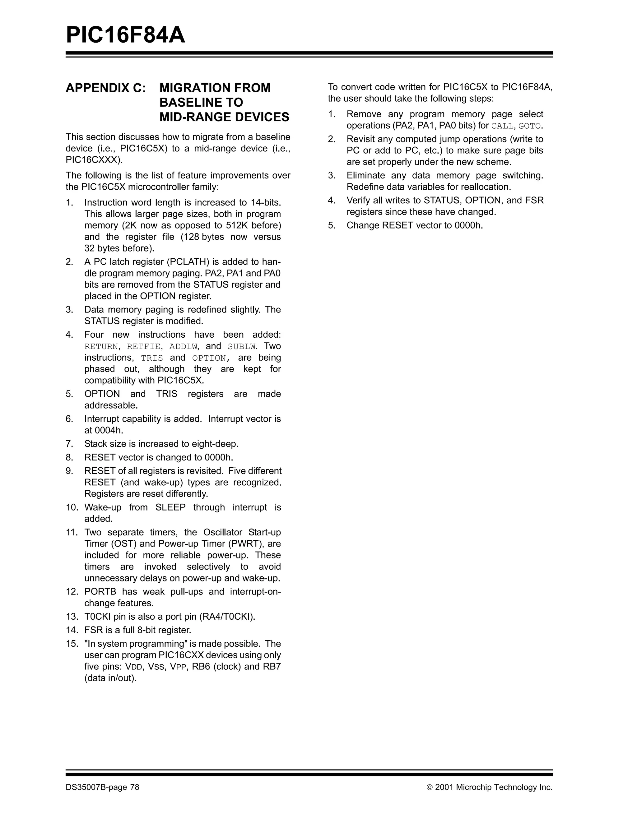
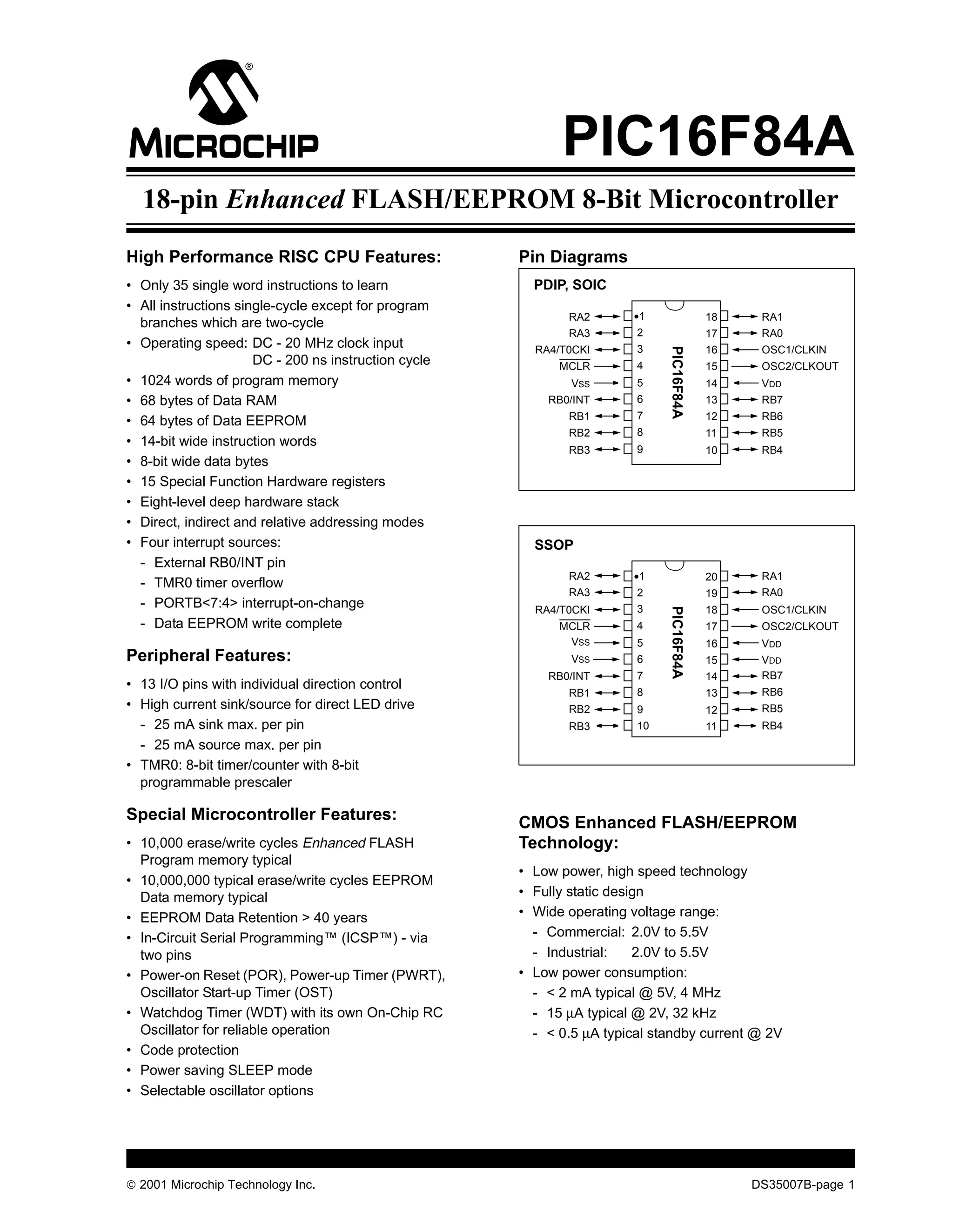
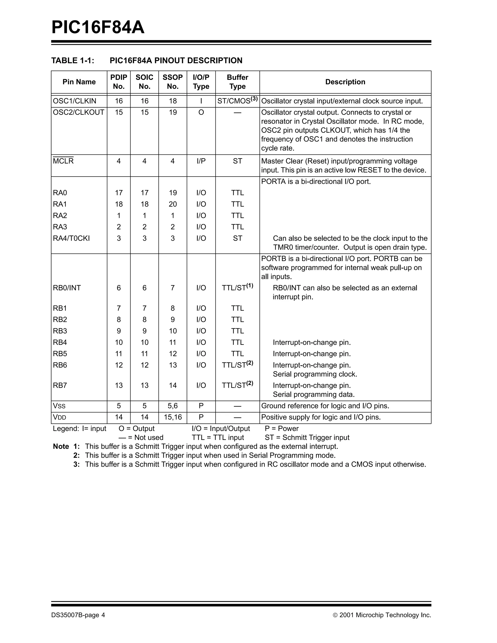
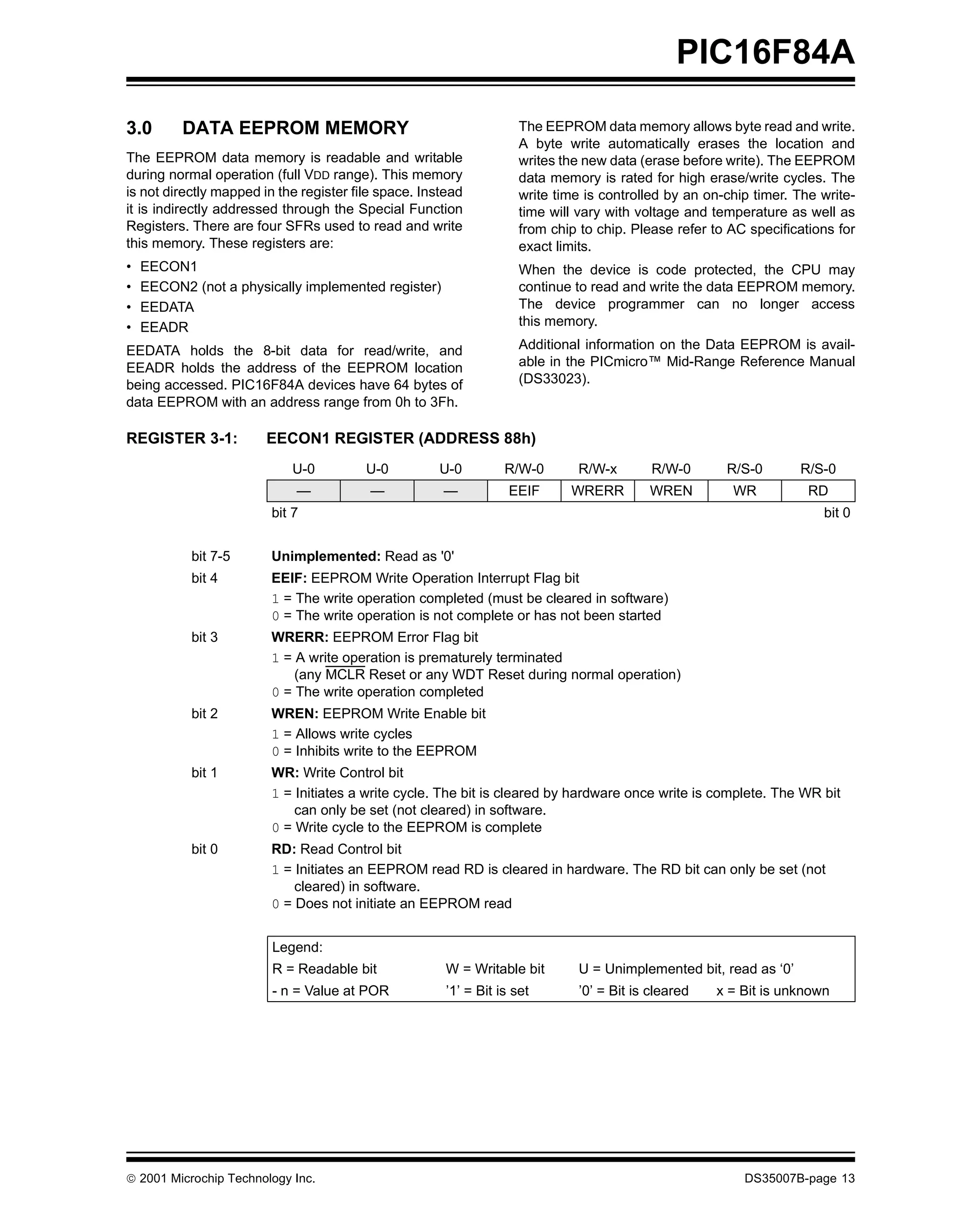
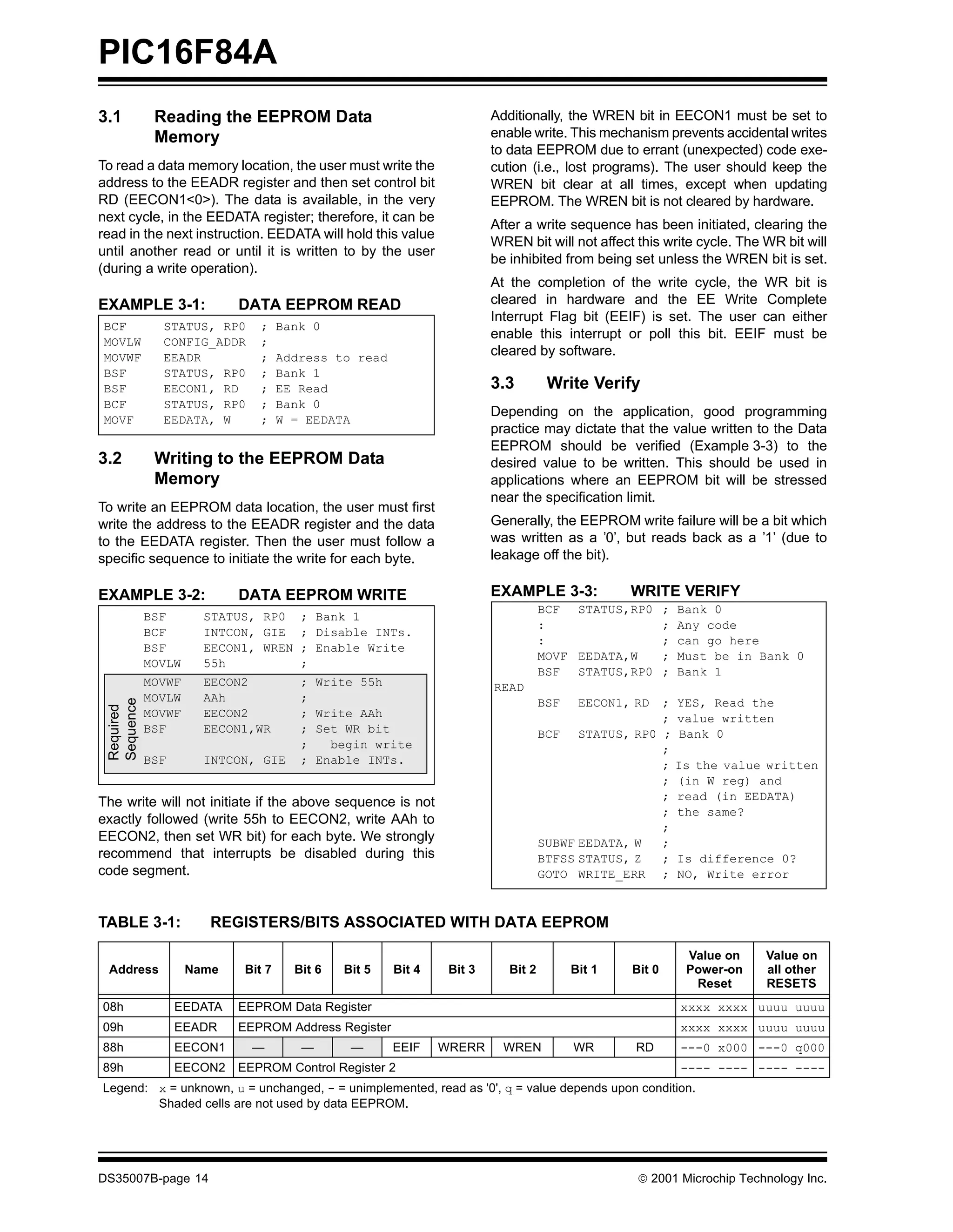
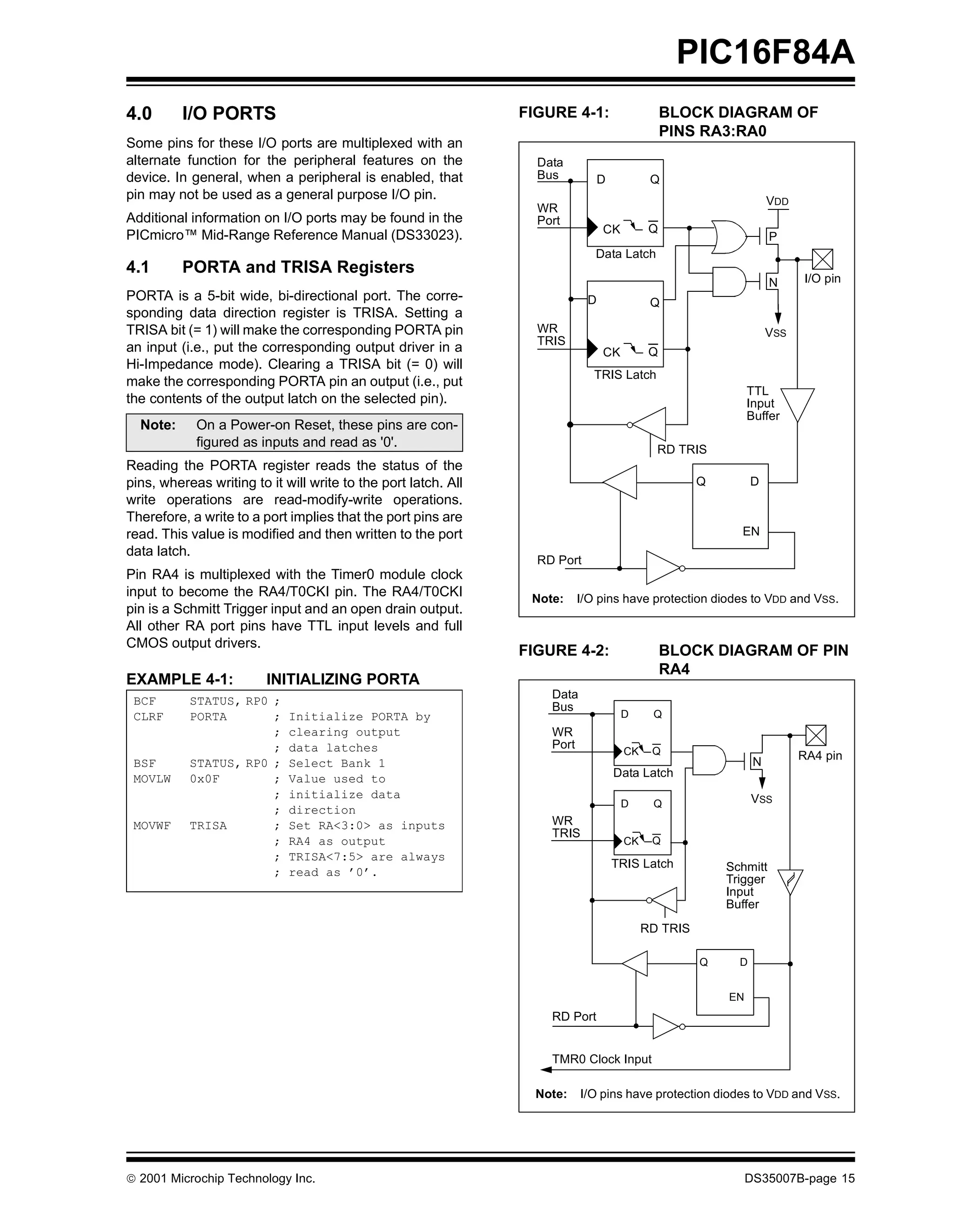
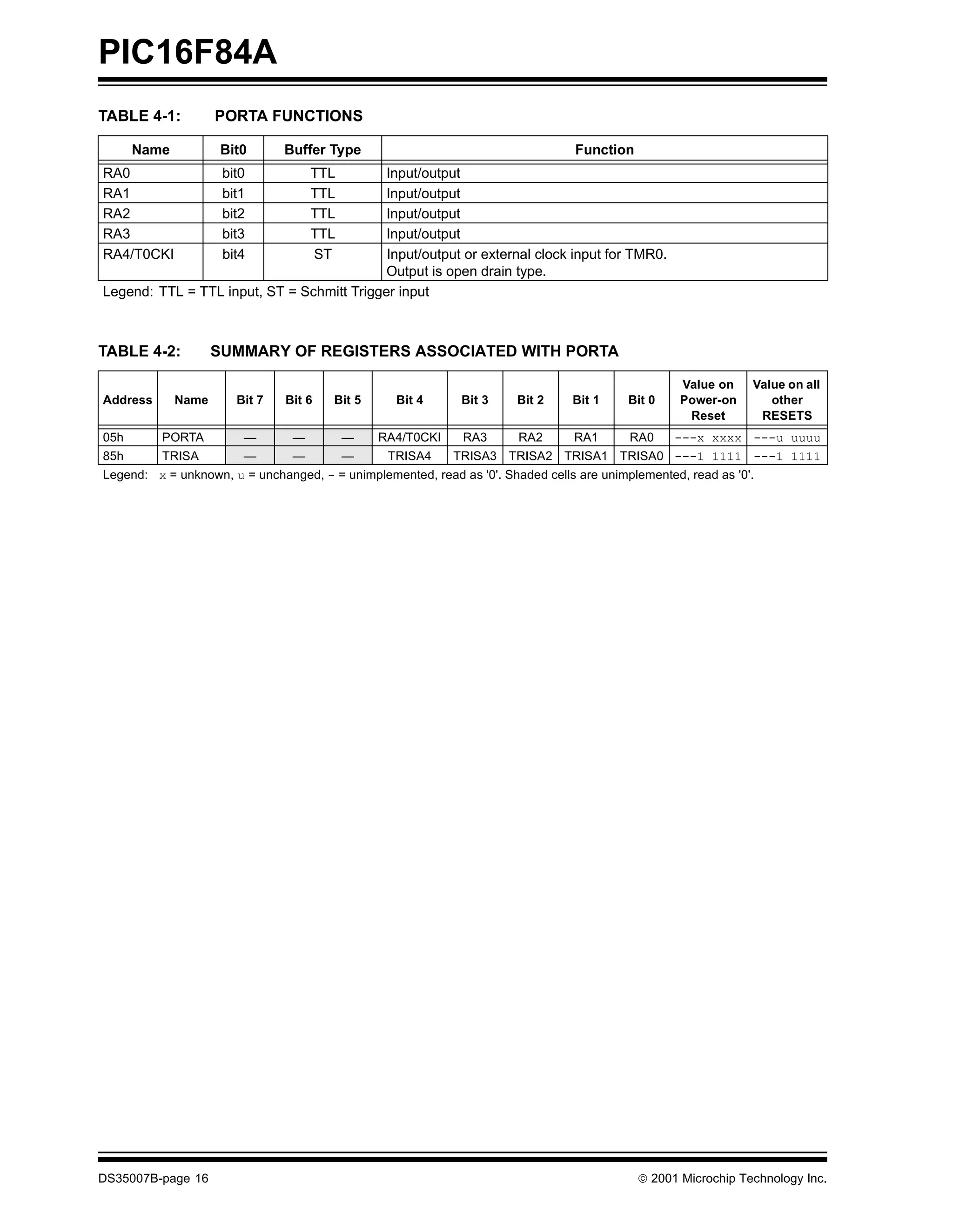
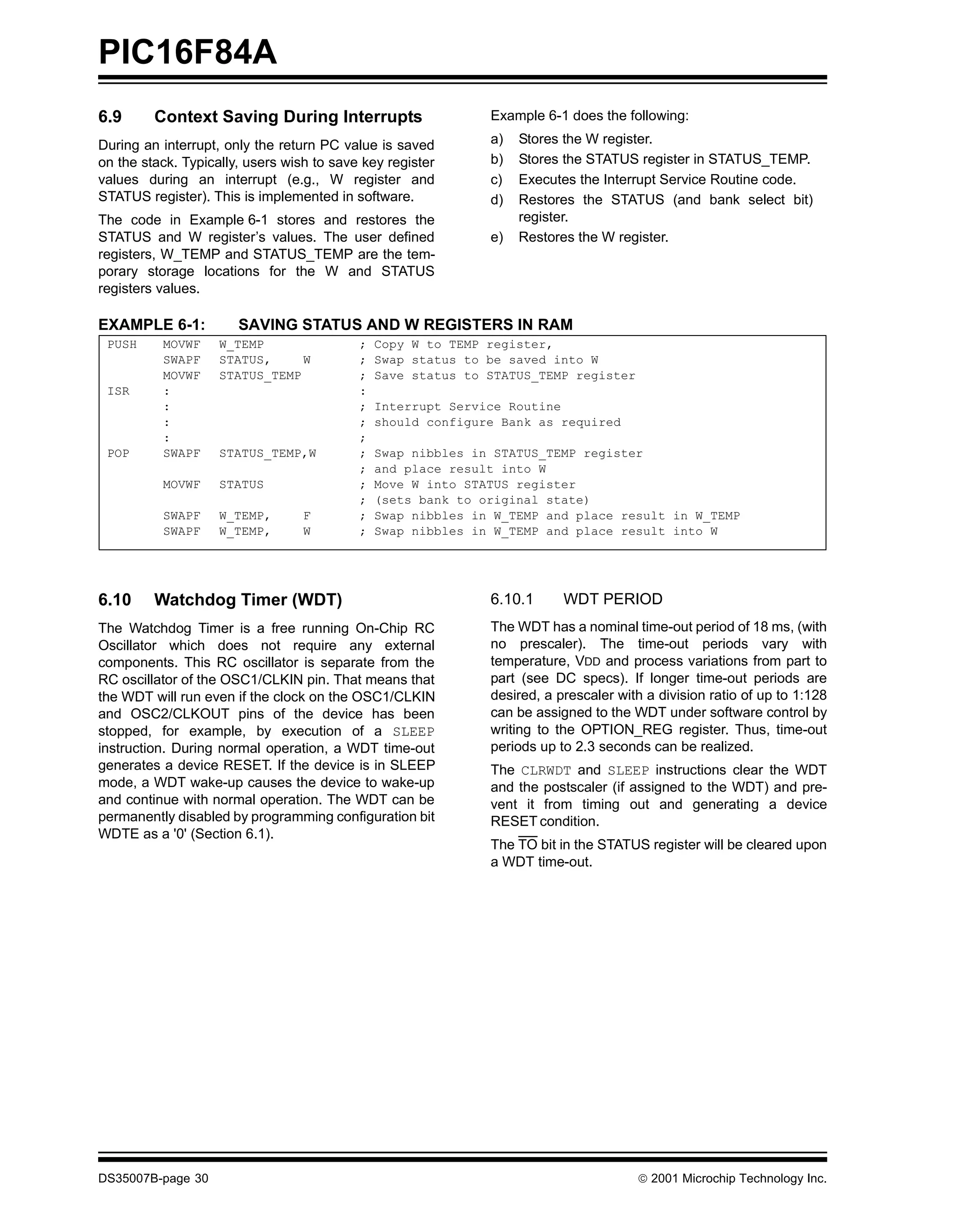
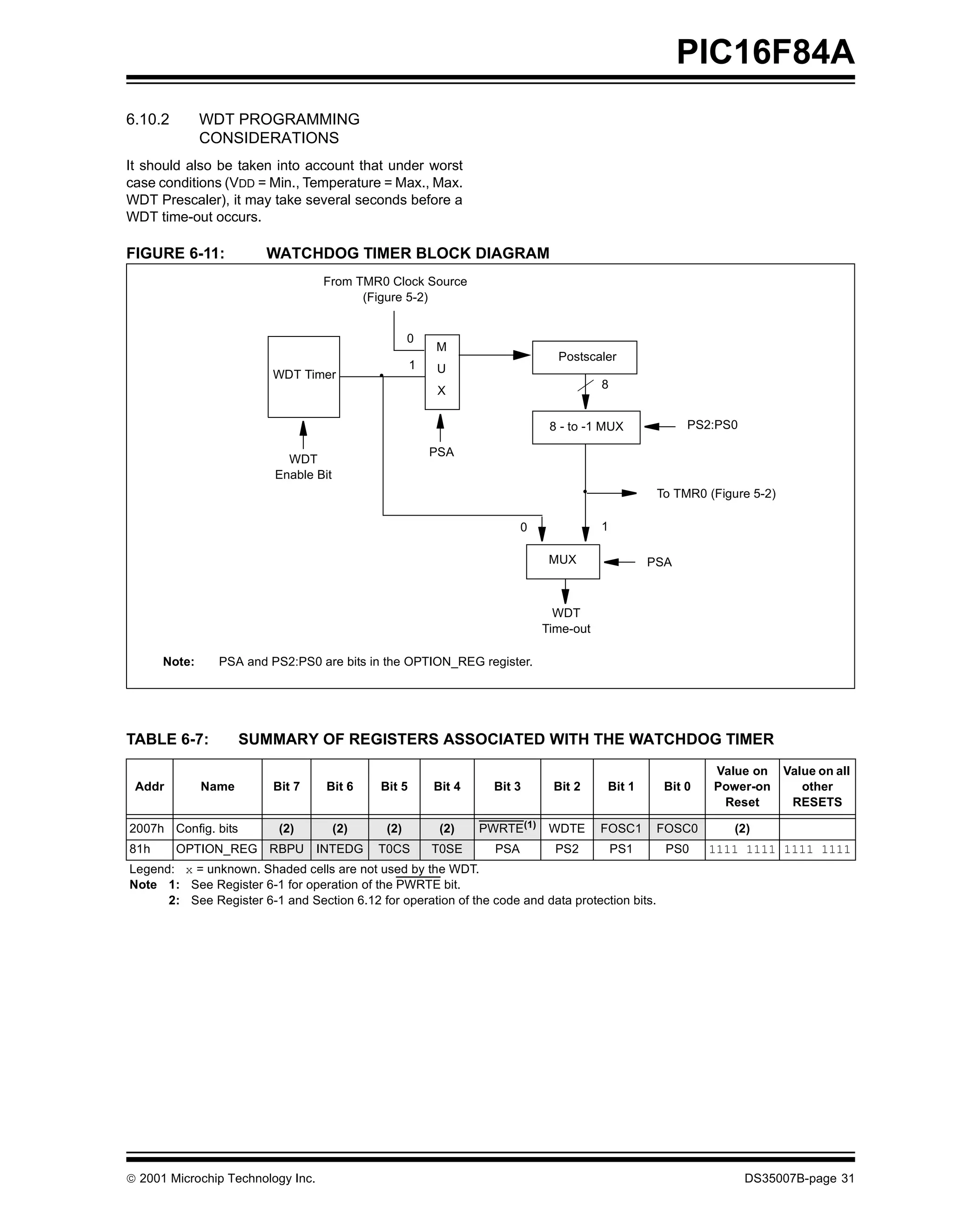
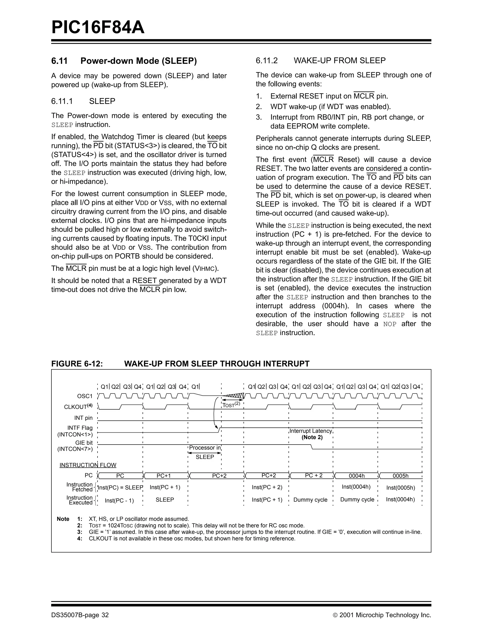
The document describes the Microchip PIC16F84A microcontroller. It is an 8-bit microcontroller with 1024 words of program
memory, 68 bytes of data RAM, and 64 bytes of data EEPROM. It has various peripherals like a timer, I/O pins, and serial
programming capability. The document provides details on the CPU architecture, memory, peripherals, and programming
features of the PIC16F84A microcontroller.

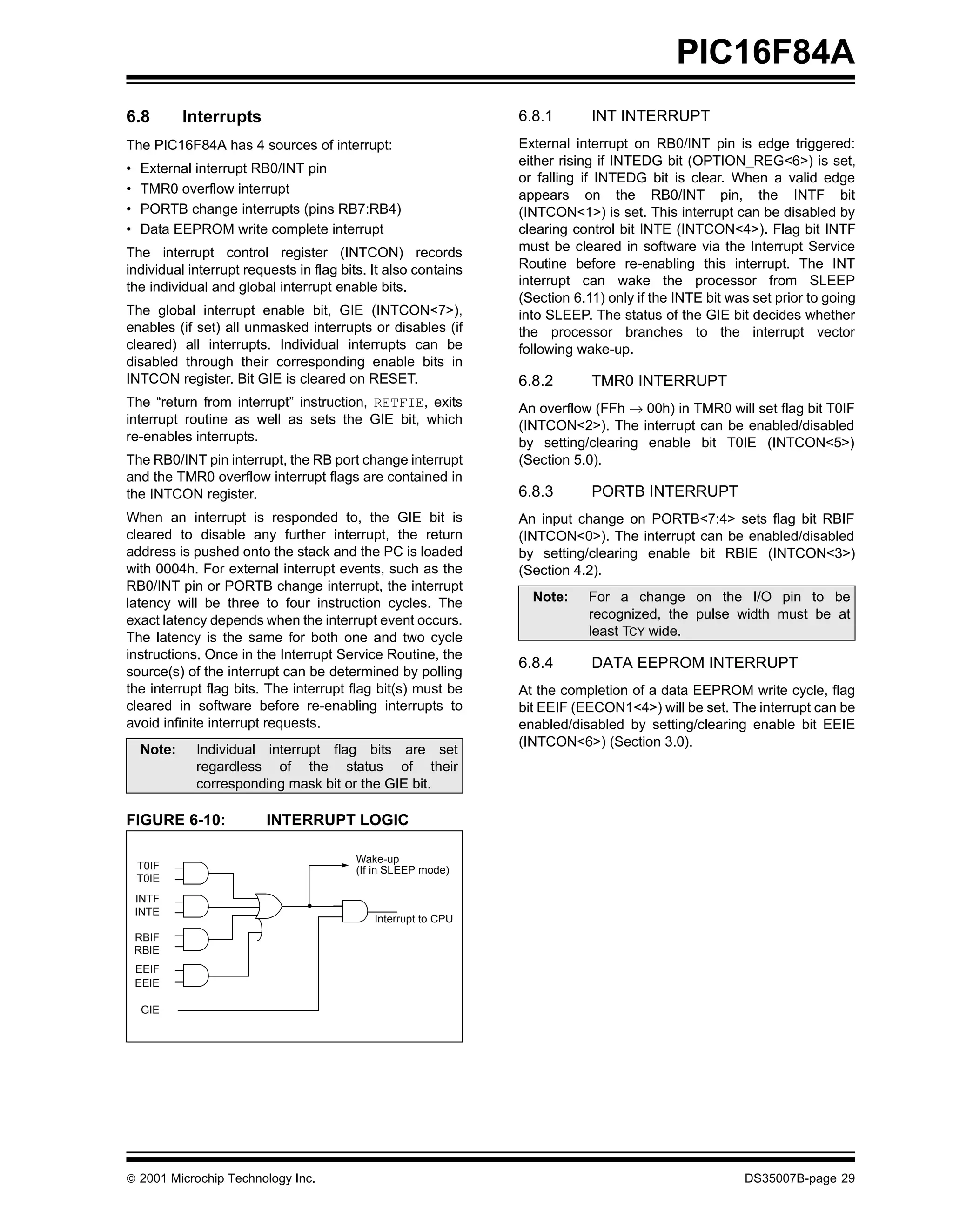
![PIC16F84A
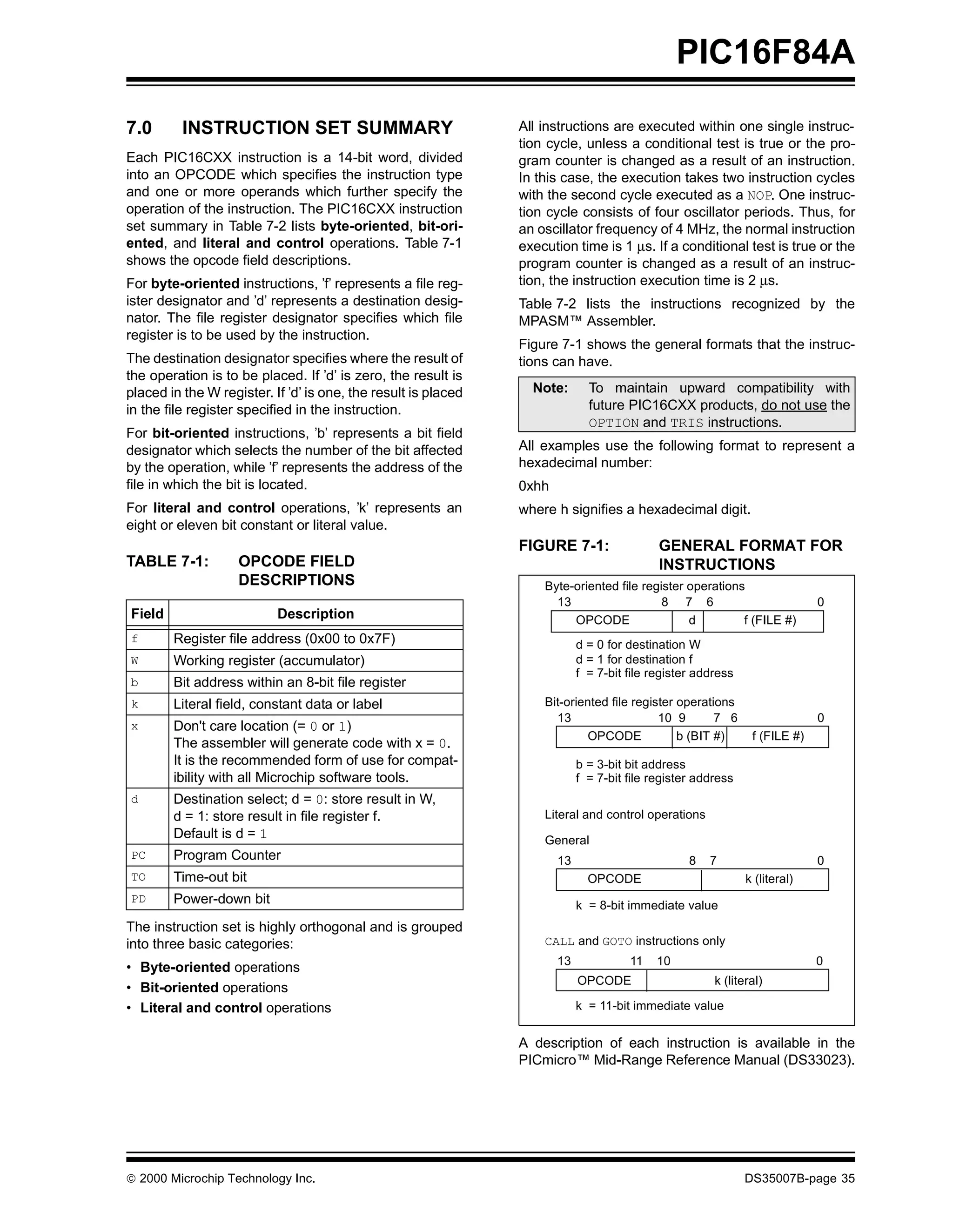
7.1 Instruction Descriptions
ADDLW Add Literal and W BCF Bit Clear f
Syntax: [label] ADDLW k Syntax: [label] BCF f,b
Operands: 0 ≤ k ≤ 255 Operands: 0 ≤ f ≤ 127
Operation: (W) + k → (W) 0≤b≤7
Status Affected: C, DC, Z Operation: 0 → (f<b>)
Description: The contents of the W register Status Affected: None
are added to the eight-bit literal ’k’ Description: Bit 'b' in register 'f' is cleared.
and the result is placed in the W
register.
ADDWF Add W and f BSF Bit Set f
Syntax: [label] ADDWF f,d Syntax: [label] BSF f,b
Operands: 0 ≤ f ≤ 127 Operands: 0 ≤ f ≤ 127
d ∈ [0,1] 0≤b≤7
Operation: (W) + (f) → (destination) Operation: 1 → (f<b>)
Status Affected: C, DC, Z Status Affected: None
Description: Add the contents of the W register Description: Bit 'b' in register 'f' is set.
with register ’f’. If ’d’ is 0, the result
is stored in the W register. If ’d’ is
1, the result is stored back in
register ’f’.
ANDLW AND Literal with W BTFSS Bit Test f, Skip if Set
Syntax: [label] ANDLW k Syntax: [label] BTFSS f,b
Operands: 0 ≤ k ≤ 255 Operands: 0 ≤ f ≤ 127
Operation: (W) .AND. (k) → (W) 0≤b<7
Status Affected: Z Operation: skip if (f<b>) = 1
Description: The contents of W register are Status Affected: None
AND’ed with the eight-bit literal Description: If bit 'b' in register 'f' is '0', the next
'k'. The result is placed in the W instruction is executed.
register. If bit 'b' is '1', then the next instruc-
tion is discarded and a NOP is exe-
cuted instead, making this a 2TCY
instruction.
ANDWF AND W with f
Syntax: [label] ANDWF f,d
Operands: 0 ≤ f ≤ 127
d ∈ [0,1]
Operation: (W) .AND. (f) → (destination)
Status Affected: Z
Description: AND the W register with register
'f'. If 'd' is 0, the result is stored in
the W register. If 'd' is 1, the result
is stored back in register 'f'.
© 2000 Microchip Technology Inc. DS35007B-page 37](https://image.slidesharecdn.com/test-090804052053-phpapp02/75/Test-39-2048.jpg)
![PIC16F84A
BTFSC Bit Test, Skip if Clear CLRWDT Clear Watchdog Timer
Syntax: [label] BTFSC f,b Syntax: [ label ] CLRWDT
Operands: 0 ≤ f ≤ 127 Operands: None
0≤b≤7 Operation: 00h → WDT
Operation: skip if (f<b>) = 0 0 → WDT prescaler,
Status Affected: None 1 → TO
1 → PD
Description: If bit ’b’ in register ’f’ is ’1’, the next
instruction is executed. Status Affected: TO, PD
If bit ’b’ in register ’f’ is ’0’, the next Description: CLRWDT instruction resets the
instruction is discarded, and a NOP Watchdog Timer. It also resets the
is executed instead, making this a prescaler of the WDT. Status bits
2TCY instruction. TO and PD are set.
CALL Call Subroutine COMF Complement f
Syntax: [ label ] CALL k Syntax: [ label ] COMF f,d
Operands: 0 ≤ k ≤ 2047 Operands: 0 ≤ f ≤ 127
Operation: (PC)+ 1→ TOS, d ∈ [0,1]
k → PC<10:0>, Operation: (f) → (destination)
(PCLATH<4:3>) → PC<12:11>
Status Affected: Z
Status Affected: None
Description: The contents of register ’f’ are
Description: Call Subroutine. First, return complemented. If ’d’ is 0, the
address (PC+1) is pushed onto result is stored in W. If ’d’ is 1, the
the stack. The eleven-bit immedi- result is stored back in register ’f’.
ate address is loaded into PC bits
<10:0>. The upper bits of the PC
are loaded from PCLATH. CALL is
a two-cycle instruction.
CLRF Clear f DECF Decrement f
Syntax: [label] CLRF f Syntax: [label] DECF f,d
Operands: 0 ≤ f ≤ 127 Operands: 0 ≤ f ≤ 127
d ∈ [0,1]
Operation: 00h → (f)
1→Z Operation: (f) - 1 → (destination)
Status Affected: Z Status Affected: Z
Description: The contents of register ’f’ are Description: Decrement register ’f’. If ’d’ is 0,
cleared and the Z bit is set. the result is stored in the W regis-
ter. If ’d’ is 1, the result is stored
back in register ’f’.
CLRW Clear W
Syntax: [ label ] CLRW
Operands: None
Operation: 00h → (W)
1→Z
Status Affected: Z
Description: W register is cleared. Zero bit (Z)
is set.
DS35007B-page 38 © 2000 Microchip Technology Inc.](https://image.slidesharecdn.com/test-090804052053-phpapp02/75/Test-40-2048.jpg)
![PIC16F84A
DECFSZ Decrement f, Skip if 0 INCFSZ Increment f, Skip if 0
Syntax: [ label ] DECFSZ f,d Syntax: [ label ] INCFSZ f,d
Operands: 0 ≤ f ≤ 127 Operands: 0 ≤ f ≤ 127
d ∈ [0,1] d ∈ [0,1]
Operation: (f) - 1 → (destination); Operation: (f) + 1 → (destination),
skip if result = 0 skip if result = 0
Status Affected: None Status Affected: None
Description: The contents of register ’f’ are Description: The contents of register ’f’ are
decremented. If ’d’ is 0, the result incremented. If ’d’ is 0, the result is
is placed in the W register. If ’d’ is placed in the W register. If ’d’ is 1,
1, the result is placed back in the result is placed back in
register ’f’. register ’f’.
If the result is 1, the next instruc- If the result is 1, the next instruc-
tion is executed. If the result is 0, tion is executed. If the result is 0,
then a NOP is executed instead, a NOP is executed instead, making
making it a 2TCY instruction. it a 2TCY instruction.
GOTO Unconditional Branch IORLW Inclusive OR Literal with W
Syntax: [ label ] GOTO k Syntax: [ label ] IORLW k
Operands: 0 ≤ k ≤ 2047 Operands: 0 ≤ k ≤ 255
Operation: k → PC<10:0> Operation: (W) .OR. k → (W)
PCLATH<4:3> → PC<12:11> Status Affected: Z
Status Affected: None Description: The contents of the W register are
Description: GOTO is an unconditional branch. OR’ed with the eight-bit literal 'k'.
The eleven-bit immediate value is The result is placed in the W
loaded into PC bits <10:0>. The register.
upper bits of PC are loaded from
PCLATH<4:3>. GOTO is a two-
cycle instruction.
INCF Increment f IORWF Inclusive OR W with f
Syntax: [ label ] INCF f,d Syntax: [ label ] IORWF f,d
Operands: 0 ≤ f ≤ 127 Operands: 0 ≤ f ≤ 127
d ∈ [0,1] d ∈ [0,1]
Operation: (f) + 1 → (destination) Operation: (W) .OR. (f) → (destination)
Status Affected: Z Status Affected: Z
Description: The contents of register ’f’ are Description: Inclusive OR the W register with
incremented. If ’d’ is 0, the result register 'f'. If 'd' is 0, the result is
is placed in the W register. If ’d’ is placed in the W register. If 'd' is 1,
1, the result is placed back in the result is placed back in
register ’f’. register 'f'.
© 2000 Microchip Technology Inc. DS35007B-page 39](https://image.slidesharecdn.com/test-090804052053-phpapp02/75/Test-41-2048.jpg)
![PIC16F84A
MOVF Move f RETFIE Return from Interrupt
Syntax: [ label ] MOVF f,d Syntax: [ label ] RETFIE
Operands: 0 ≤ f ≤ 127 Operands: None
d ∈ [0,1] Operation: TOS → PC,
Operation: (f) → (destination) 1 → GIE
Status Affected: Z Status Affected: None
Description: The contents of register f are
moved to a destination dependant
upon the status of d. If d = 0, des-
tination is W register. If d = 1, the
destination is file register f itself.
d = 1 is useful to test a file register,
since status flag Z is affected.
MOVLW Move Literal to W RETLW Return with Literal in W
Syntax: [ label ] MOVLW k Syntax: [ label ] RETLW k
Operands: 0 ≤ k ≤ 255 Operands: 0 ≤ k ≤ 255
Operation: k → (W) Operation: k → (W);
TOS → PC
Status Affected: None
Status Affected: None
Description: The eight-bit literal ’k’ is loaded
into W register. The don’t cares Description: The W register is loaded with the
will assemble as 0’s. eight-bit literal 'k'. The program
counter is loaded from the top of
the stack (the return address).
This is a two-cycle instruction.
MOVWF Move W to f RETURN Return from Subroutine
Syntax: [ label ] MOVWF f Syntax: [ label ] RETURN
Operands: 0 ≤ f ≤ 127 Operands: None
Operation: (W) → (f) Operation: TOS → PC
Status Affected: None Status Affected: None
Description: Move data from W register to Description: Return from subroutine. The stack
register 'f'. is POPed and the top of the stack
(TOS) is loaded into the program
counter. This is a two-cycle
instruction.
NOP No Operation
Syntax: [ label ] NOP
Operands: None
Operation: No operation
Status Affected: None
Description: No operation.
DS35007B-page 40 © 2000 Microchip Technology Inc.](https://image.slidesharecdn.com/test-090804052053-phpapp02/75/Test-42-2048.jpg)
![PIC16F84A
RLF Rotate Left f through Carry SUBLW Subtract W from Literal
Syntax: [ label ] RLF f,d Syntax: [ label ] SUBLW k
Operands: 0 ≤ f ≤ 127 Operands: 0 ≤ k ≤ 255
d ∈ [0,1] Operation: k - (W) → (W)
Operation: See description below Status Affected: C, DC, Z
Status Affected: C Description: The W register is subtracted (2’s
Description: The contents of register ’f’ are complement method) from the
rotated one bit to the left through eight-bit literal 'k'. The result is
the Carry Flag. If ’d’ is 0, the placed in the W register.
result is placed in the W register.
If ’d’ is 1, the result is stored back
in register ’f’.
C Register f
RRF Rotate Right f through Carry SUBWF Subtract W from f
Syntax: [ label ] RRF f,d Syntax: [ label ] SUBWF f,d
Operands: 0 ≤ f ≤ 127 Operands: 0 ≤ f ≤ 127
d ∈ [0,1] d ∈ [0,1]
Operation: See description below Operation: (f) - (W) → (destination)
Status Affected: C Status Affected: C, DC, Z
Description: The contents of register ’f’ are Description: Subtract (2’s complement method)
rotated one bit to the right through W register from register 'f'. If 'd' is 0,
the Carry Flag. If ’d’ is 0, the result the result is stored in the W regis-
is placed in the W register. If ’d’ is ter. If 'd' is 1, the result is stored
1, the result is placed back in back in register 'f'.
register ’f’.
C Register f
SLEEP SWAPF Swap Nibbles in f
Syntax: [ label ] SLEEP Syntax: [ label ] SWAPF f,d
Operands: None Operands: 0 ≤ f ≤ 127
d ∈ [0,1]
Operation: 00h → WDT,
0 → WDT prescaler, Operation: (f<3:0>) → (destination<7:4>),
1 → TO, (f<7:4>) → (destination<3:0>)
0 → PD Status Affected: None
Status Affected: TO, PD Description: The upper and lower nibbles of
Description: The power-down status bit, PD is register 'f' are exchanged. If 'd' is
cleared. Time-out status bit, TO 0, the result is placed in W regis-
is set. Watchdog Timer and its ter. If 'd' is 1, the result is placed in
prescaler are cleared. register 'f'.
The processor is put into SLEEP
mode with the oscillator stopped.
© 2000 Microchip Technology Inc. DS35007B-page 41](https://image.slidesharecdn.com/test-090804052053-phpapp02/75/Test-43-2048.jpg)
![PIC16F84A
XORLW Exclusive OR Literal with W XORWF Exclusive OR W with f
Syntax: [label] XORLW k Syntax: [label] XORWF f,d
Operands: 0 ≤ k ≤ 255 Operands: 0 ≤ f ≤ 127
Operation: (W) .XOR. k → (W) d ∈ [0,1]
Status Affected: Z Operation: (W) .XOR. (f) → (destination)
Description: The contents of the W register Status Affected: Z
are XOR’ed with the eight-bit lit- Description: Exclusive OR the contents of the
eral 'k'. The result is placed in W register with register 'f'. If 'd' is
the W register. 0, the result is stored in the W
register. If 'd' is 1, the result is
stored back in register 'f'.
DS35007B-page 42 © 2000 Microchip Technology Inc.](https://image.slidesharecdn.com/test-090804052053-phpapp02/75/Test-44-2048.jpg)