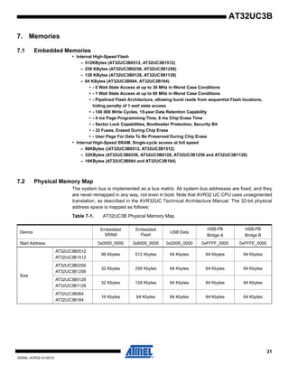
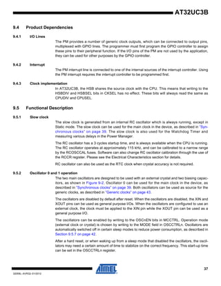
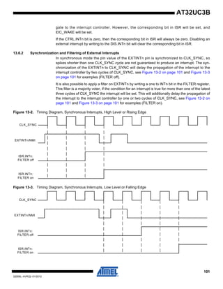
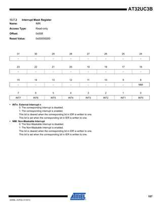
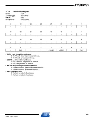
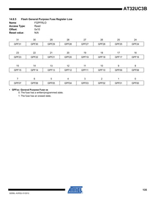
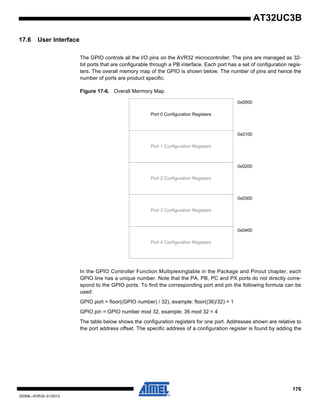
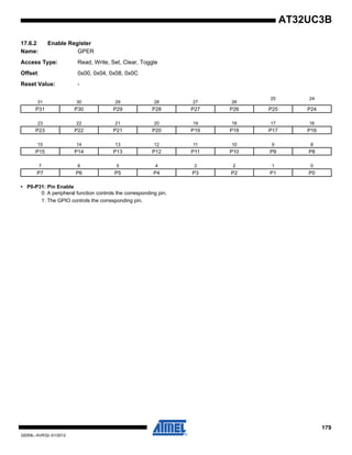
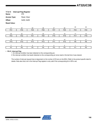
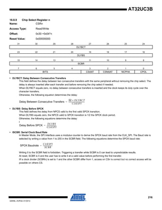
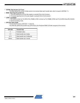
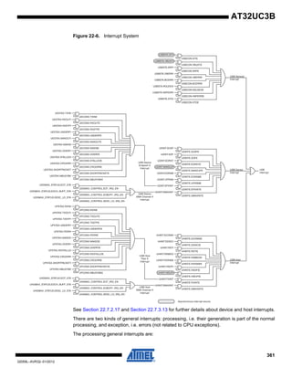
The AT32UC3B is a 32-bit AVR microcontroller with features such as:
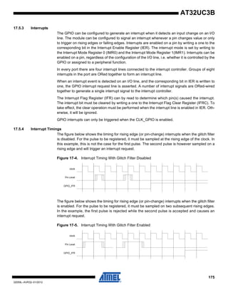
- Up to 512KB flash memory and 96KB SRAM
- USB device and embedded host interfaces
- Three USARTs, SPI, TWI, and other communication interfaces
- PWM, timer/counter, analog to digital converter, and other peripherals
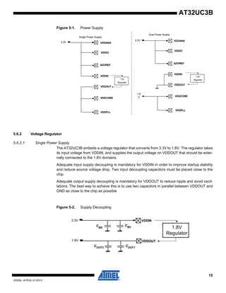
- On-chip debug system and Nexus 2.0 interface for debugging


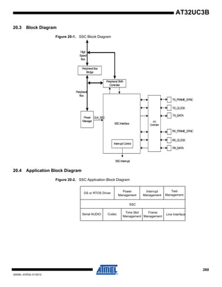
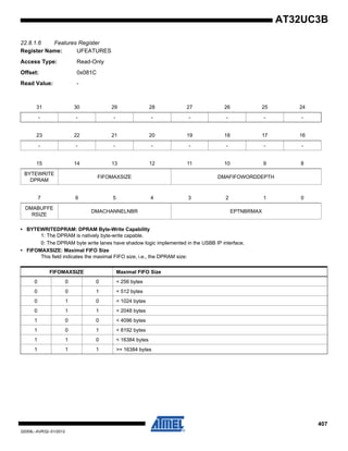
![4
32059L–AVR32–01/2012
AT32UC3B
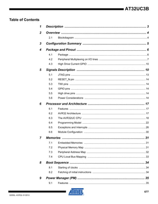
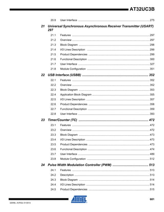
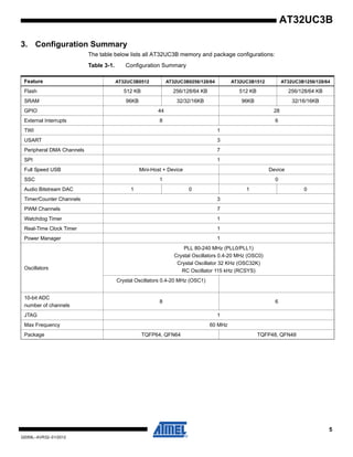
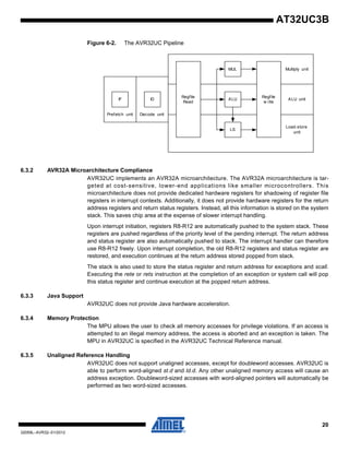
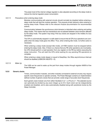
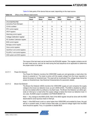
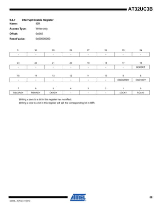
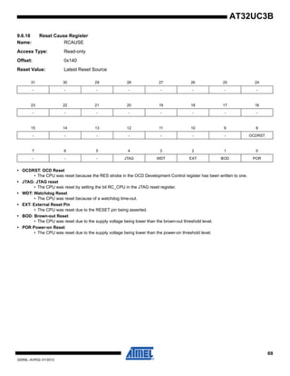
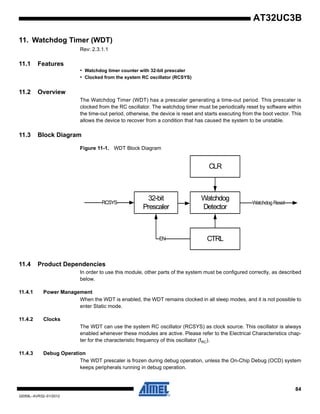
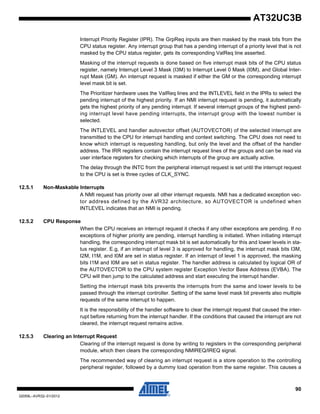
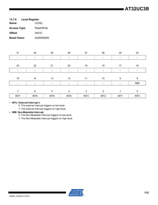
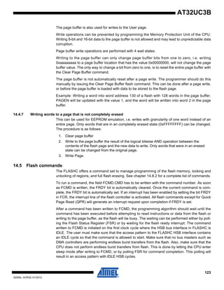
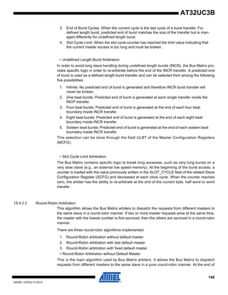
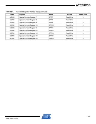
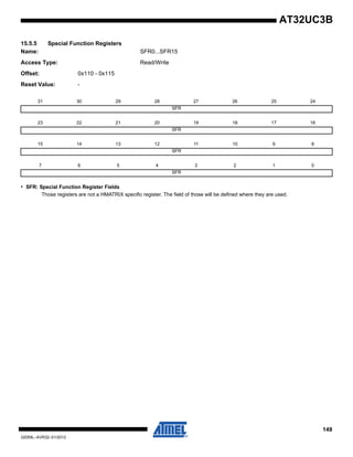
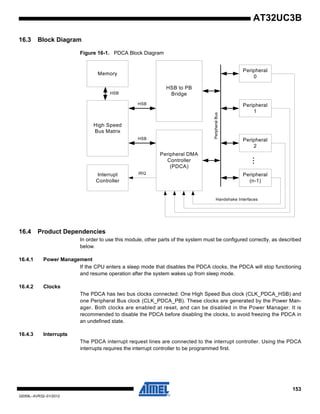
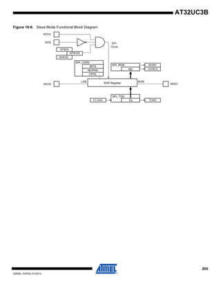
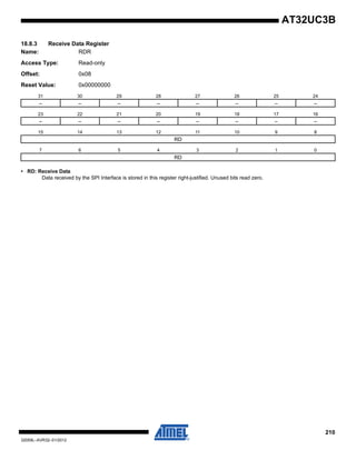
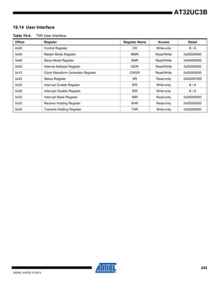
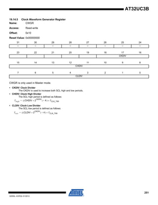
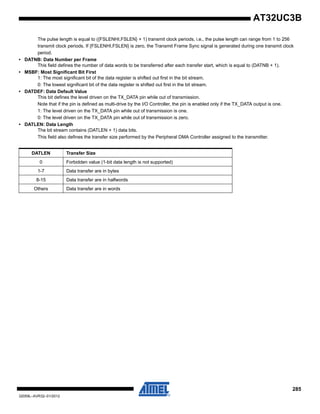
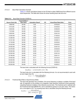
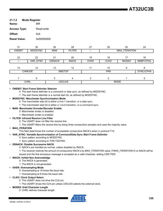
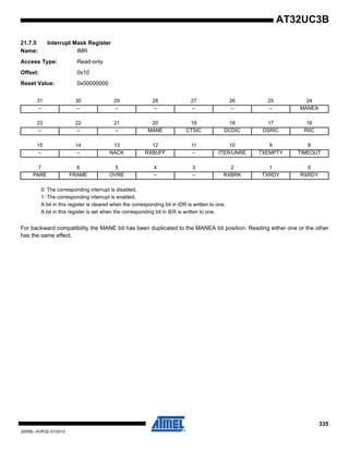
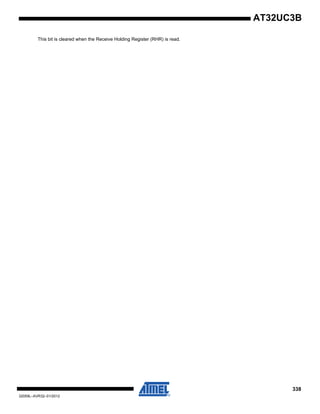
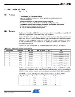
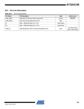
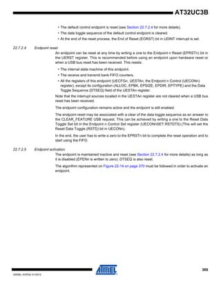
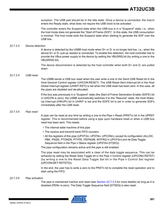
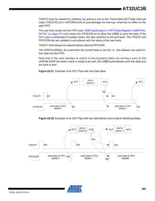
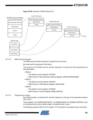
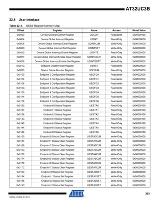
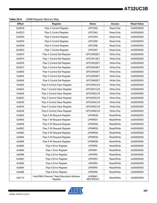
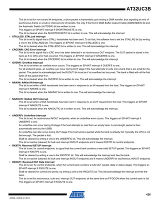
2. Overview
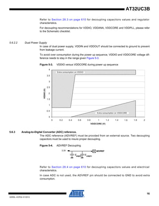
2.1 Blockdiagram
Figure 2-1. Block diagram
TIMER/COUNTER
INTERRUPT
CONTROLLER
REAL TIME
COUNTER
PERIPHERAL
DMA
CONTROLLER
HSB-PB
BRIDGE B
HSB-PB
BRIDGE A
S
M M M
S
S
M
EXTERNAL
INTERRUPT
CONTROLLER
HIGH SPEED
BUS MATRIX
GENERALPURPOSEIOs
GENERALPURPOSEIOs
PA
PB
A[2..0]
B[2..0]
CLK[2..0]
EXTINT[7..0]
KPS[7..0]
NMI
GCLK[3..0]
XIN32
XOUT32
XIN0
XOUT0
PA
PB
RESET_N
32 KHz
OSC
115 kHz
RCOSC
OSC0
PLL0
SERIAL
PERIPHERAL
INTERFACE
TWO-WIRE
INTERFACE
PDCPDC
MISO, MOSI
NPCS[3..0]
SCL
SDA
USART1
PDC
RXD
TXD
CLK
RTS, CTS
DSR, DTR, DCD, RI
USART0
USART2
PDC
RXD
TXD
CLK
RTS, CTS
SYNCHRONOUS
SERIAL
CONTROLLER
PDC
TX_CLOCK, TX_FRAME_SYNC
RX_DATA
TX_DATA
RX_CLOCK, RX_FRAME_SYNC
ANALOG TO
DIGITAL
CONVERTER
PDC
AD[7..0]
ADVREF
WATCHDOG
TIMER
XIN1
XOUT1
OSC1
PLL1
SCK
JTAG
INTERFACE
MCKO
MDO[5..0]
MSEO[1..0]
EVTI_N
TCK
TDO
TDI
TMS
POWER
MANAGER
RESET
CONTROLLER
SLEEP
CONTROLLER
CLOCK
CONTROLLER
CLOCK
GENERATOR
CONFIGURATION REGISTERS BUS
PB
PB
HSBHSB
S
FLASH
CONTROLLER
M
S
USB
INTERFACE
DMA
ID
VBOF
VBUS
D-
D+
EVTO_N
AVR32 UC
CPUNEXUS
CLASS 2+
OCD
INSTR
INTERFACE
DATA
INTERFACE
MEMORYINTERFACE
FAST GPIO
16/32/96 KB
SRAM
MEMORY PROTECTION UNIT
LOCAL BUS
INTERFACE
AUDIO
BITSTREAM
DAC
PDC
DATA[1..0]
DATAN[1..0]
PULSE WIDTH
MODULATION
CONTROLLER
PWM[6..0]
64/128/
256/512 KB
FLASH](https://image.slidesharecdn.com/doc32059-150506085255-conversion-gate02/85/Doc32059-4-320.jpg)
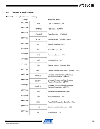
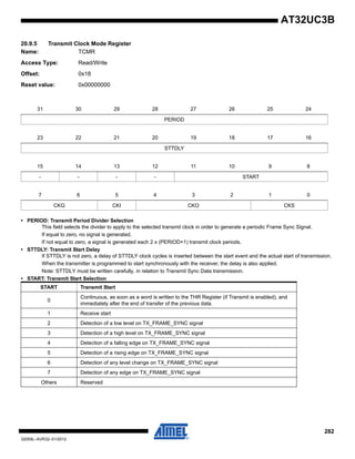
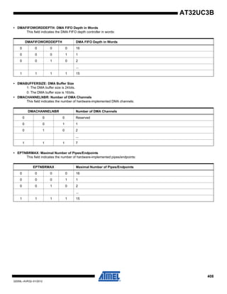
![7
32059L–AVR32–01/2012
AT32UC3B
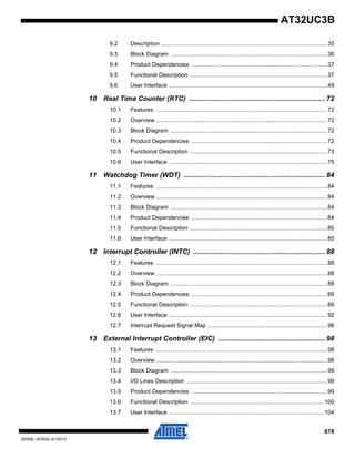
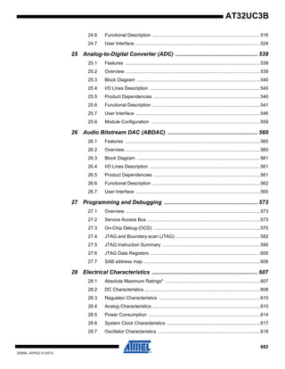
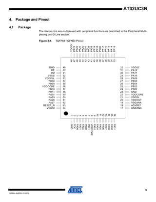
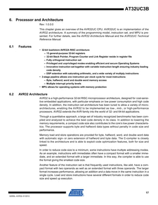
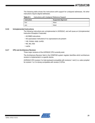
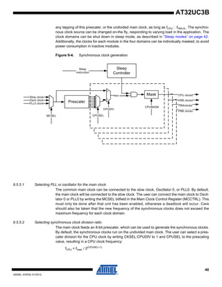
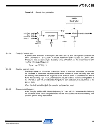
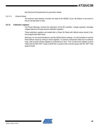
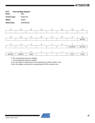
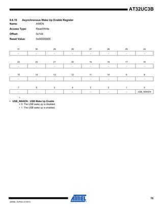
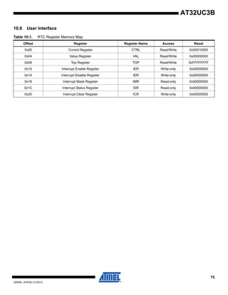
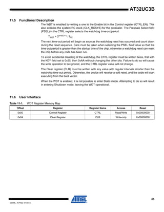
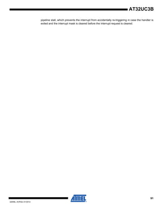
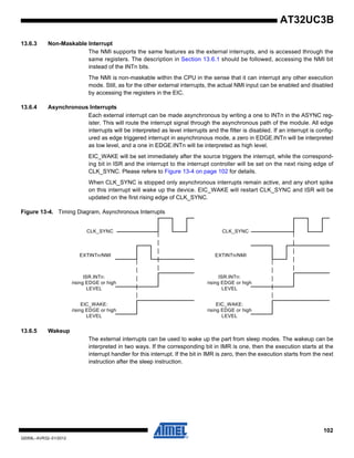
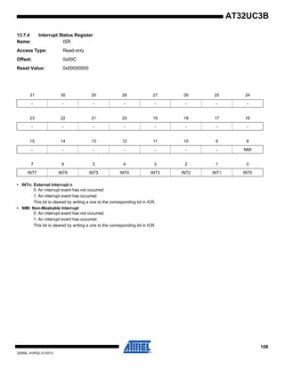
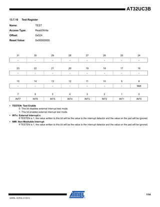
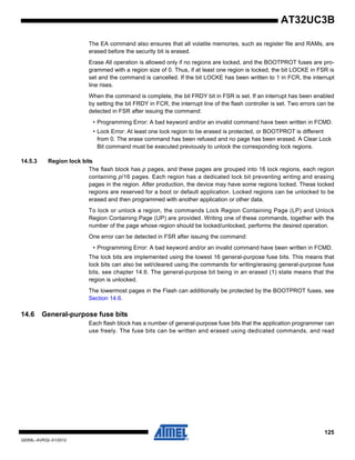
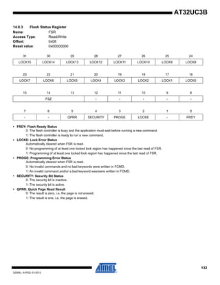
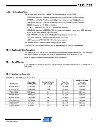
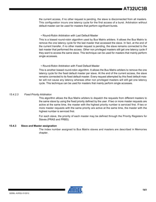
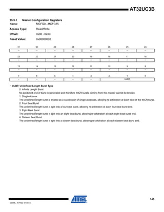
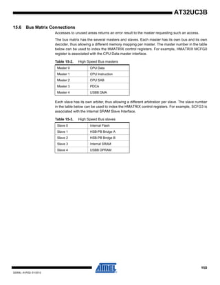
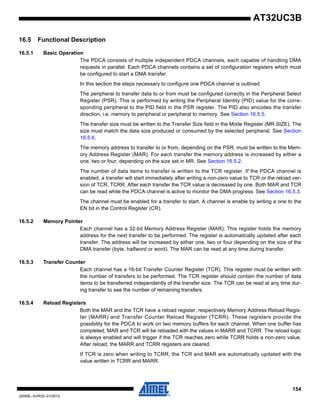
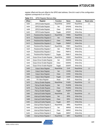
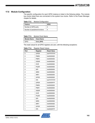
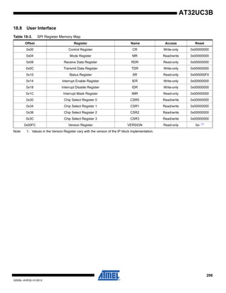
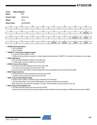
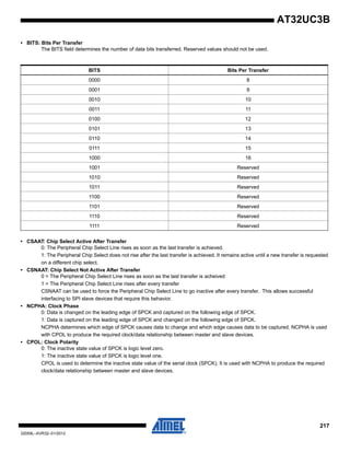
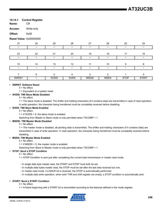
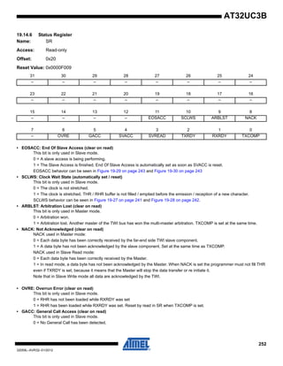
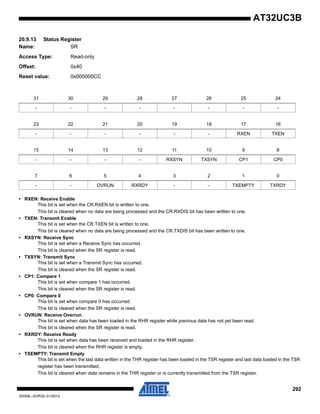
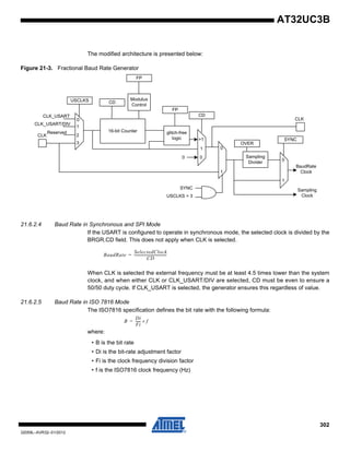
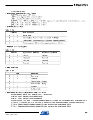
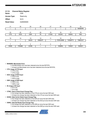
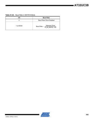
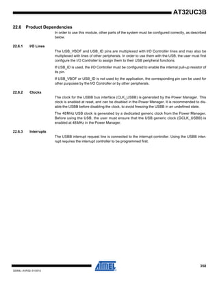
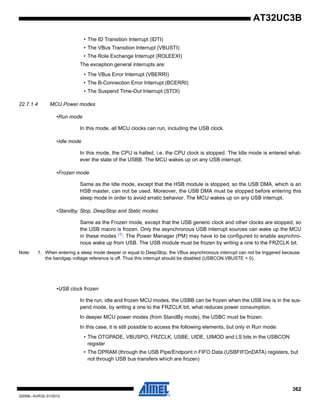
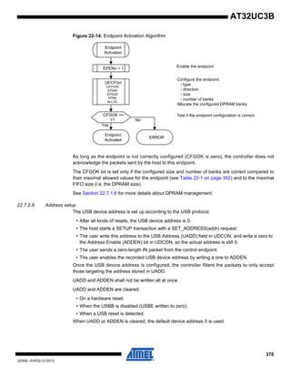
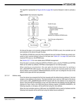
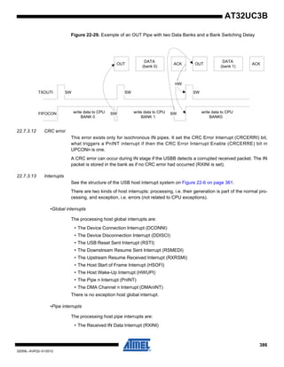
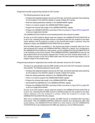
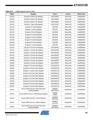
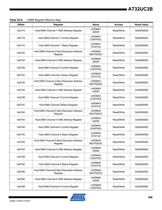
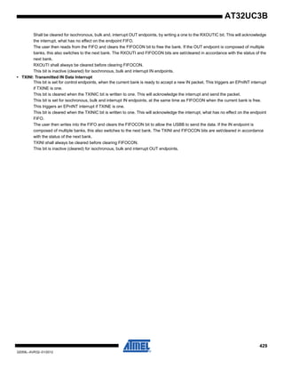
Figure 4-2. TQFP48 / QFN48 Pinout
Note: The exposed pad is not connected to anything internally, but should be soldered to ground to
increase board level reliability.
4.2 Peripheral Multiplexing on I/O lines
4.2.1 Multiplexed signals
Each GPIO line can be assigned to one of 4 peripheral functions; A, B, C or D (D is only avail-
able for UC3Bx512 parts). The following table define how the I/O lines on the peripherals A, B,C
or D are multiplexed by the GPIO.
GND1
TCK2
PA003
PA014
PA025
VDDCORE6
PA037
PA048
PA059
PA0610
PA0711
PA0812
GNDANA13
ADVREF14
VDDANA15
VDDOUT16
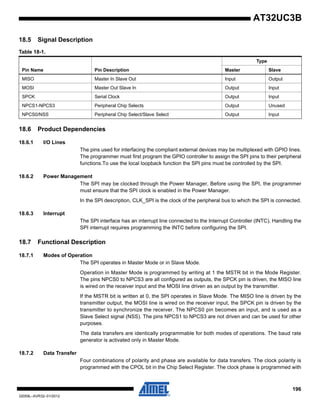
VDDIN17
VDDCORE18
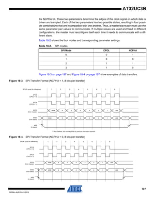
GND19
PA0920
PA1021
PA1122
PA1223
VDDIO24
VDDIO36
PA2335
PA2234
PA2133
PA2032
PA1931
PA1830
PA1729
PA1628
PA1527
PA1426
PA1325
GND 37
DP 38
DM 39
VBUS 40
VDDPLL 41
VDDCORE 42
PA24 43
PA25 44
PA26 45
PA27 46
RESET_N 47
VDDIO 48
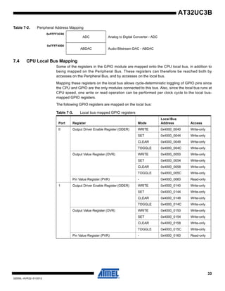
Table 4-1. GPIO Controller Function Multiplexing
48-pin 64-pin PIN GPIO Pin Function A Function B Function C
Function D
(only for UC3Bx512)
3 3 PA00 GPIO 0
4 4 PA01 GPIO 1
5 5 PA02 GPIO 2
7 9 PA03 GPIO 3 ADC - AD[0] PM - GCLK[0] USBB - USB_ID ABDAC - DATA[0]
8 10 PA04 GPIO 4 ADC - AD[1] PM - GCLK[1] USBB - USB_VBOF ABDAC - DATAN[0]
9 11 PA05 GPIO 5 EIC - EXTINT[0] ADC - AD[2] USART1 - DCD ABDAC - DATA[1]](https://image.slidesharecdn.com/doc32059-150506085255-conversion-gate02/85/Doc32059-7-320.jpg)
![8
32059L–AVR32–01/2012
AT32UC3B
10 12 PA06 GPIO 6 EIC - EXTINT[1] ADC - AD[3] USART1 - DSR ABDAC - DATAN[1]
11 13 PA07 GPIO 7 PWM - PWM[0] ADC - AD[4] USART1 - DTR
SSC -
RX_FRAME_SYNC
12 14 PA08 GPIO 8 PWM - PWM[1] ADC - AD[5] USART1 - RI SSC - RX_CLOCK
20 28 PA09 GPIO 9 TWI - SCL SPI0 - NPCS[2] USART1 - CTS
21 29 PA10 GPIO 10 TWI - SDA SPI0 - NPCS[3] USART1 - RTS
22 30 PA11 GPIO 11 USART0 - RTS TC - A2 PWM - PWM[0] SSC - RX_DATA
23 31 PA12 GPIO 12 USART0 - CTS TC - B2 PWM - PWM[1] USART1 - TXD
25 33 PA13 GPIO 13 EIC - NMI PWM - PWM[2] USART0 - CLK SSC - RX_CLOCK
26 34 PA14 GPIO 14 SPI0 - MOSI PWM - PWM[3] EIC - EXTINT[2] PM - GCLK[2]
27 35 PA15 GPIO 15 SPI0 - SCK PWM - PWM[4] USART2 - CLK
28 36 PA16 GPIO 16 SPI0 - NPCS[0] TC - CLK1 PWM - PWM[4]
29 37 PA17 GPIO 17 SPI0 - NPCS[1] TC - CLK2 SPI0 - SCK USART1 - RXD
30 39 PA18 GPIO 18 USART0 - RXD PWM - PWM[5] SPI0 - MISO
SSC -
RX_FRAME_SYNC
31 40 PA19 GPIO 19 USART0 - TXD PWM - PWM[6] SPI0 - MOSI SSC - TX_CLOCK
32 44 PA20 GPIO 20 USART1 - CLK TC - CLK0 USART2 - RXD SSC - TX_DATA
33 45 PA21 GPIO 21 PWM - PWM[2] TC - A1 USART2 - TXD
SSC -
TX_FRAME_SYNC
34 46 PA22 GPIO 22 PWM - PWM[6] TC - B1 ADC - TRIGGER ABDAC - DATA[0]
35 47 PA23 GPIO 23 USART1 - TXD SPI0 - NPCS[1] EIC - EXTINT[3] PWM - PWM[0]
43 59 PA24 GPIO 24 USART1 - RXD SPI0 - NPCS[0] EIC - EXTINT[4] PWM - PWM[1]
44 60 PA25 GPIO 25 SPI0 - MISO PWM - PWM[3] EIC - EXTINT[5]
45 61 PA26 GPIO 26 USBB - USB_ID USART2 - TXD TC - A0 ABDAC - DATA[1]
46 62 PA27 GPIO 27 USBB - USB_VBOF USART2 - RXD TC - B0 ABDAC - DATAN[1]
41 PA28 GPIO 28 USART0 - CLK PWM - PWM[4] SPI0 - MISO ABDAC - DATAN[0]
42 PA29 GPIO 29 TC - CLK0 TC - CLK1 SPI0 - MOSI
15 PA30 GPIO 30 ADC - AD[6] EIC - SCAN[0] PM - GCLK[2]
16 PA31 GPIO 31 ADC - AD[7] EIC - SCAN[1] PWM - PWM[6]
6 PB00 GPIO 32 TC - A0 EIC - SCAN[2] USART2 - CTS
7 PB01 GPIO 33 TC - B0 EIC - SCAN[3] USART2 - RTS
24 PB02 GPIO 34 EIC - EXTINT[6] TC - A1 USART1 - TXD
25 PB03 GPIO 35 EIC - EXTINT[7] TC - B1 USART1 - RXD
26 PB04 GPIO 36 USART1 - CTS SPI0 - NPCS[3] TC - CLK2
27 PB05 GPIO 37 USART1 - RTS SPI0 - NPCS[2] PWM - PWM[5]
38 PB06 GPIO 38 SSC - RX_CLOCK USART1 - DCD EIC - SCAN[4] ABDAC - DATA[0]
43 PB07 GPIO 39 SSC - RX_DATA USART1 - DSR EIC - SCAN[5] ABDAC - DATAN[0]
54 PB08 GPIO 40
SSC -
RX_FRAME_SYNC
USART1 - DTR EIC - SCAN[6] ABDAC - DATA[1]
Table 4-1. GPIO Controller Function Multiplexing](https://image.slidesharecdn.com/doc32059-150506085255-conversion-gate02/85/Doc32059-8-320.jpg)
![9
32059L–AVR32–01/2012
AT32UC3B
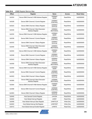
4.2.2 JTAG Port Connections
If the JTAG is enabled, the JTAG will take control over a number of pins, irrespective of the I/O
Controller configuration.
4.2.3 Nexus OCD AUX port connections
If the OCD trace system is enabled, the trace system will take control over a number of pins, irre-
spectively of the PIO configuration. Two different OCD trace pin mappings are possible,
depending on the configuration of the OCD AXS register. For details, see the AVR32 UC Tech-
nical Reference Manual.
4.2.4 Oscillator Pinout
The oscillators are not mapped to the normal A, B or C functions and their muxings are con-
trolled by registers in the Power Manager (PM). Please refer to the power manager chapter for
more information about this.
55 PB09 GPIO 41 SSC - TX_CLOCK USART1 - RI EIC - SCAN[7] ABDAC - DATAN[1]
57 PB10 GPIO 42 SSC - TX_DATA TC - A2 USART0 - RXD
58 PB11 GPIO 43
SSC -
TX_FRAME_SYNC
TC - B2 USART0 - TXD
Table 4-1. GPIO Controller Function Multiplexing
Table 4-2. JTAG Pinout
64QFP/QFN 48QFP/QFN Pin name JTAG pin
2 2 TCK TCK
3 3 PA00 TDI
4 4 PA01 TDO
5 5 PA02 TMS
Table 4-3. Nexus OCD AUX port connections
Pin AXS=0 AXS=1
EVTI_N PB05 PA14
MDO[5] PB04 PA08
MDO[4] PB03 PA07
MDO[3] PB02 PA06
MDO[2] PB01 PA05
MDO[1] PB00 PA04
MDO[0] PA31 PA03
EVTO_N PA15 PA15
MCKO PA30 PA13
MSEO[1] PB06 PA09
MSEO[0] PB07 PA10](https://image.slidesharecdn.com/doc32059-150506085255-conversion-gate02/85/Doc32059-9-320.jpg)
![28
32059L–AVR32–01/2012
AT32UC3B
status register. Upon entry into Debug mode, hardware sets the SR[D] bit and jumps to the
Debug Exception handler. By default, Debug mode executes in the exception context, but with
dedicated Return Address Register and Return Status Register. These dedicated registers
remove the need for storing this data to the system stack, thereby improving debuggability. The
mode bits in the status register can freely be manipulated in Debug mode, to observe registers
in all contexts, while retaining full privileges.
Debug mode is exited by executing the retd instruction. This returns to the previous context.
6.5.5 Entry Points for Events
Several different event handler entry points exists. In AVR32UC, the reset address is
0x8000_0000. This places the reset address in the boot flash memory area.
TLB miss exceptions and scall have a dedicated space relative to EVBA where their event han-
dler can be placed. This speeds up execution by removing the need for a jump instruction placed
at the program address jumped to by the event hardware. All other exceptions have a dedicated
event routine entry point located relative to EVBA. The handler routine address identifies the
exception source directly.
AVR32UC uses the ITLB and DTLB protection exceptions to signal a MPU protection violation.
ITLB and DTLB miss exceptions are used to signal that an access address did not map to any of
the entries in the MPU. TLB multiple hit exception indicates that an access address did map to
multiple TLB entries, signalling an error.
All external interrupt requests have entry points located at an offset relative to EVBA. This
autovector offset is specified by an external Interrupt Controller. The programmer must make
sure that none of the autovector offsets interfere with the placement of other code. The autovec-
tor offset has 14 address bits, giving an offset of maximum 16384 bytes.
Special considerations should be made when loading EVBA with a pointer. Due to security con-
siderations, the event handlers should be located in non-writeable flash memory, or optionally in
a privileged memory protection region if an MPU is present.
If several events occur on the same instruction, they are handled in a prioritized way. The priority
ordering is presented in Table 6-4. If events occur on several instructions at different locations in
the pipeline, the events on the oldest instruction are always handled before any events on any
younger instruction, even if the younger instruction has events of higher priority than the oldest
instruction. An instruction B is younger than an instruction A if it was sent down the pipeline later
than A.
The addresses and priority of simultaneous events are shown in Table 6-4. Some of the excep-
tions are unused in AVR32UC since it has no MMU, coprocessor interface, or floating-point unit.](https://image.slidesharecdn.com/doc32059-150506085255-conversion-gate02/85/Doc32059-28-320.jpg)
![38
32059L–AVR32–01/2012
AT32UC3B
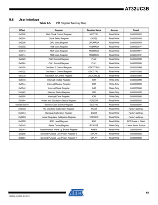
The PM masks the oscillator outputs during the start-up time, to ensure that no unstable clocks
propagate to the digital logic. The OSCnRDY bits in POSCSR are automatically set and cleared
according to the status of the oscillators. A zero to one transition on these bits can also be con-
figured to generate an interrupt, as described in ”MODE: Oscillator Mode” on page 57.
Figure 9-2. Oscillator connections
9.5.3 32 KHz oscillator operation
The 32 KHz oscillator operates as described for Oscillator 0 and 1 above. The 32 KHz oscillator
is used as source clock for the Real-Time Counter.
The oscillator is disabled by default, but can be enabled by writing OSC32EN in OSCCTRL32.
The oscillator is an ultra-low power design and remains enabled in all sleep modes except Static
mode.
While the 32 KHz oscillator is disabled, the XIN32 and XOUT32 pins are available as general
purpose I/Os. When the oscillator is configured to work with an external clock (MODE field in
OSCCTRL32 register), the external clock must be connected to XIN32 while the XOUT32 pin
can be used as a general purpose I/O.
The startup time of the 32 KHz oscillator can be set in the OSCCTRL32, after which OSC32RDY
in POSCSR is set. An interrupt can be generated on a zero to one transition of OSC32RDY.
As a crystal oscillator usually requires a very long startup time (up to 1 second), the 32 KHz
oscillator will keep running across resets, except Power-On-Reset.
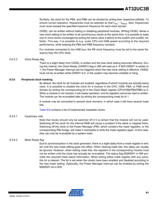
9.5.4 PLL operation
The device contains two PLLs, PLL0 and PLL1. These are disabled by default, but can be
enabled to provide high frequency source clocks for synchronous or generic clocks. The PLLs
can take either Oscillator 0 or 1 as reference clock. The PLL output is divided by a multiplication
factor, and the PLL compares the resulting clock to the reference clock. The PLL will adjust its
output frequency until the two compared clocks are equal, thus locking the output frequency to a
multiple of the reference clock frequency.
The Voltage Controlled Oscillator inside the PLL can generate frequencies from 80 to 240 MHz.
To make the PLL output frequencies under 80 MHz the OTP[1] bitfield could be set. This will
divide the output of the PLL by two and bring the clock in range of the max frequency of the
CPU.
XIN
XOUT
C2
C1](https://image.slidesharecdn.com/doc32059-150506085255-conversion-gate02/85/Doc32059-38-320.jpg)
![39
32059L–AVR32–01/2012
AT32UC3B
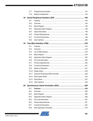
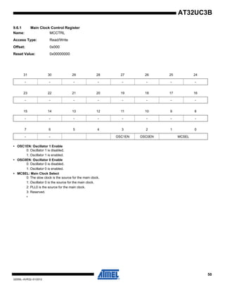
When the PLL is switched on, or when changing the clock source or multiplication factor for the
PLL, the PLL is unlocked and the output frequency is undefined. The PLL clock for the digital
logic is automatically masked when the PLL is unlocked, to prevent connected digital logic from
receiving a too high frequency and thus become unstable.
Figure 9-3. PLL with control logic and filters
9.5.4.1 Enabling the PLL
PLLn is enabled by writing the PLLEN bit in the PLLn register. PLLOSC selects Oscillator 0 or 1
as clock source. The PLLMUL and PLLDIV bitfields must be written with the multiplication and
division factors, respectively, creating the voltage controlled ocillator frequency fVCO and the PLL
frequency fPLL :
fVCO = (PLLMUL+1)/(PLLDIV) • fOSC if PLLDIV > 0.
fVCO = 2*(PLLMUL+1) • fOSC if PLLDIV = 0.
If PLLOPT[1] field is set to 0:
fPLL = fVCO.
If PLLOPT[1] field is set to 1:
fPLL = fVCO / 2.
The PLLn:PLLOPT field should be set to proper values according to the PLL operating fre-
quency. The PLLOPT field can also be set to divide the output frequency of the PLLs by 2.
The lock signal for each PLL is available as a LOCKn flag in POSCSR. An interrupt can be gen-
erated on a 0 to 1 transition of these bits.
9.5.5 Synchronous clocks
The slow clock (default), Oscillator 0, or PLL0 provide the source for the main clock, which is the
common root for the synchronous clocks for the CPU/HSB, PBA, and PBB modules. The main
clock is divided by an 8-bit prescaler, and each of these four synchronous clocks can run from
P h a s e
D e te c to r
O u tp u t
D iv id e r
0
1
O s c 0
c lo c k
O s c 1
c lo c k
P L L O S C P L L O P T
P L L M U L
L o c k b it
M a s k P L L c lo c k
In p u t
D iv id e r
P L L D IV
1 /2
P L L O P T [1 ]
0
1
V C O
fv c o
fP L L
L o c k
D e te c to r](https://image.slidesharecdn.com/doc32059-150506085255-conversion-gate02/85/Doc32059-39-320.jpg)
![52
32059L–AVR32–01/2012
AT32UC3B
9.6.3 Clock Mask Register
Name: CPU/HSB/PBA/PBBMASK
Access Type: Read/Write
Offset: 0x008, 0x00C, 0x010, 0x014
Reset Value: -
31 30 29 28 27 26 25 24
MASK[31:24]
23 22 21 20 19 18 17 16
MASK[23:16]
15 14 13 12 11 10 9 8
MASK[15:8]
7 6 5 4 3 2 1 0
MASK[7:0]](https://image.slidesharecdn.com/doc32059-150506085255-conversion-gate02/85/Doc32059-52-320.jpg)
![54
32059L–AVR32–01/2012
AT32UC3B
9.6.4 PLL Control Register
Name: PLL0,1
Access Type: Read/Write
Offset: 0x020, 0x024
Reset Value: 0x00000000
• PLLCOUNT: PLL Count
Specifies the number of slow clock cycles before ISR:LOCKn will be set after PLLn has been written, or after PLLn has been
automatically re-enabled after exiting a sleep mode.
• PLLMUL: PLL Multiply Factor
• PLLDIV: PLL Division Factor
These fields determine the ratio of the ouput frequency of the internal VCO of the PLL (fVCO) to the source oscillator frequency:
• fVCO = (PLLMUL+1)/(PLLDIV) * fOSC if PLLDIV > 0.
• fVCO = 2 * (PLLMUL+1) * fOSC if PLLDIV = 0.
If PLLOPT[1] bit is set to 0: fPLL = fVCO.
If PLLOPT[1] bit is set to 1: fPLL = fVCO / 2.
Note that the PLLMUL field cannot be equal to 0 or 1, or the behavior of the PLL will be undefined.
PLLDIV gives also the input frequency of the PLL (fIN):
if the PLLDIV field is set to 0: fIN = fOSC.
if the PLLDIV field is greater than 0: fIN = fOSC / (2 * PLLDIV).
• PLLOPT: PLL Option
Select the operating range for the PLL.
PLLOPT[0]: Select the VCO frequency range.
PLLOPT[1]: Enable the extra output divider.
PLLOPT[2]: Disable the Wide-Bandwidth mode (Wide-Bandwidth mode allows a faster startup time and out-of-lock time).
•
31 30 29 28 27 26 25 24
- - PLLCOUNT
23 22 21 20 19 18 17 16
- - - - PLLMUL
15 14 13 12 11 10 9 8
- - - - PLLDIV
7 6 5 4 3 2 1 0
- - - PLLOPT PLLOSC PLLEN](https://image.slidesharecdn.com/doc32059-150506085255-conversion-gate02/85/Doc32059-54-320.jpg)
![55
32059L–AVR32–01/2012
AT32UC3B
•
•
• PLLOSC: PLL Oscillator Select
0: Oscillator 0 is the source for the PLL.
1: Oscillator 1 is the source for the PLL.
• PLLEN: PLL Enable
0: PLL is disabled.
1: PLL is enabled.
•
Table 9-7. PLLOPT Fields Description in AT32UC3B
Description
PLLOPT[0]: VCO frequency
0 160MHz<fvco<240MHz
1 80MHz<fvco<180MHz
PLLOPT[1]: Output divider
0 fPLL = fvco
1 fPLL = fvco/2
PLLOPT[2]
0 Wide Bandwidth Mode enabled
1 Wide Bandwidth Mode disabled](https://image.slidesharecdn.com/doc32059-150506085255-conversion-gate02/85/Doc32059-55-320.jpg)

![64
32059L–AVR32–01/2012
AT32UC3B
9.6.13 Generic Clock Control Register
Name: GCCTRL
Access Type: Read/Write
Offset: 0x060 - 0x070
Reset Value: 0x00000000
There is one GCCTRL register per generic clock in the design.
• DIV: Division Factor
• DIVEN: Divide Enable
0: The generic clock equals the undivided source clock.
1: The generic clock equals the source clock divided by 2*(DIV+1).
• CEN: Clock Enable
0: Clock is stopped.
1: Clock is running.
• PLLSEL: PLL Select
0: Oscillator is source for the generic clock.
1: PLL is source for the generic clock.
• OSCSEL: Oscillator Select
0: Oscillator (or PLL) 0 is source for the generic clock.
1: Oscillator (or PLL) 1 is source for the generic clock.
31 30 29 28 27 26 25 24
- - - - - - - -
23 22 21 20 19 18 17 16
- - - - - - - -
15 14 13 12 11 10 9 8
DIV[7:0]
7 6 5 4 3 2 1 0
- - - DIVEN - CEN PLLSEL OSCSEL](https://image.slidesharecdn.com/doc32059-150506085255-conversion-gate02/85/Doc32059-64-320.jpg)
![65
32059L–AVR32–01/2012
AT32UC3B
9.6.14 RC Oscillator Calibration Register
Name: RCCR
Access Type: Read/Write
Offset: 0x0C0
Reset Value: -
• KEY: Register Write protection
This field must be written twice, first with key value 0x55, then 0xAA, for a write operation to have an effect.
• CALIB: Calibration Value
Calibration Value for the RC oscillator.
• FCD: Flash Calibration Done
• Set to 1 when the CALIB field has been updated by the Flash fuses after power-on reset or Flash fuses update.
• 0: Allow subsequent overwriting of the CALIB value by Flash fuses.
• 1: The CALIB value will not be updated again by Flash fuses.
31 30 29 28 27 26 25 24
KEY
23 22 21 20 19 18 17 16
- - - - - - - FCD
15 14 13 12 11 10 9 8
- - - - - - CALIB[9:8]
7 6 5 4 3 2 1 0
CALIB[7:0]](https://image.slidesharecdn.com/doc32059-150506085255-conversion-gate02/85/Doc32059-65-320.jpg)
![71
32059L–AVR32–01/2012
AT32UC3B
9.6.20 General Purpose Low-power Register 0/1
Name: GPLP
Access Type: Read/Write
Offset: 0x200
Reset Value: 0x00000000
These registers are general purpose 32-bit registers that are reset only by power-on-reset. Any other reset will keep the content
of these registers untouched. User software can use these registers to save context variables in a very low power mode.
Two GPLP register are implemented in AT32UC3B.
31 30 29 28 27 26 25 24
DATA[31:24]
23 22 21 20 19 18 17 16
DATA[23:16]
15 14 13 12 11 10 9 8
DATA[15:8]
7 6 5 4 3 2 1 0
DATA[7:0]](https://image.slidesharecdn.com/doc32059-150506085255-conversion-gate02/85/Doc32059-71-320.jpg)
![77
32059L–AVR32–01/2012
AT32UC3B
10.6.2 Value Register
Name: VAL
Access Type: Read/Write
Offset: 0x04
Reset Value: 0x00000000
• VAL[31:0]: RTC Value
This value is incremented on every rising edge of the source clock.
31 30 29 28 27 26 25 24
VAL[31:24]
23 22 21 20 19 18 17 16
VAL[23:16]
15 14 13 12 11 10 9 8
VAL[15:8]
7 6 5 4 3 2 1 0
VAL[7:0]](https://image.slidesharecdn.com/doc32059-150506085255-conversion-gate02/85/Doc32059-77-320.jpg)
![78
32059L–AVR32–01/2012
AT32UC3B
10.6.3 Top Register
Name: TOP
Access Type: Read/Write
Offset: 0x08
Reset Value: 0xFFFFFFFF
• VAL[31:0]: RTC Top Value
VAL wraps at this value.
31 30 29 28 27 26 25 24
VAL[31:24]
23 22 21 20 19 18 17 16
VAL[23:16]
15 14 13 12 11 10 9 8
VAL[15:8]
7 6 5 4 3 2 1 0
VAL[7:0]](https://image.slidesharecdn.com/doc32059-150506085255-conversion-gate02/85/Doc32059-78-320.jpg)


![87
32059L–AVR32–01/2012
AT32UC3B
11.6.2 Clear Register
Name: CLR
Access Type: Write-only
Offset: 0x04
Reset Value: 0x00000000
• CLR:
Writing periodically any value to this field when the WDT is enabled, within the watchdog time-out period, will prevent a
watchdog reset.
This field always reads as zero.
31 30 29 28 27 26 25 24
CLR[31:24]
23 22 21 20 19 18 17 16
CLR[23:16]
15 14 13 12 11 10 9 8
CLR[15:8]
7 6 5 4 3 2 1 0
CLR[7:0]](https://image.slidesharecdn.com/doc32059-150506085255-conversion-gate02/85/Doc32059-87-320.jpg)
![89
32059L–AVR32–01/2012
AT32UC3B
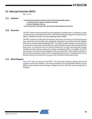
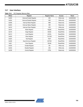
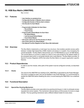
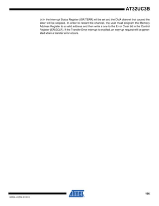
Figure 12-1. INTC Block Diagram
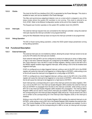
12.4 Product Dependencies
In order to use this module, other parts of the system must be configured correctly, as described
below.
12.4.1 Power Management
If the CPU enters a sleep mode that disables CLK_SYNC, the INTC will stop functioning and
resume operation after the system wakes up from sleep mode.
12.4.2 Clocks
The clock for the INTC bus interface (CLK_INTC) is generated by the Power Manager. This
clock is enabled at reset, and can be disabled in the Power Manager.
The INTC sampling logic runs on a clock which is stopped in any of the sleep modes where the
system RC oscillator is not running. This clock is referred to as CLK_SYNC. This clock is
enabled at reset, and only turned off in sleep modes where the system RC oscillator is stopped.
12.4.3 Debug Operation
When an external debugger forces the CPU into debug mode, the INTC continues normal
operation.
12.5 Functional Description
All of the incoming interrupt requests (IREQs) are sampled into the corresponding Interrupt
Request Register (IRR). The IRRs must be accessed to identify which IREQ within a group that
is active. If several IREQs within the same group are active, the interrupt service routine must
prioritize between them. All of the input lines in each group are logically ORed together to form
the GrpReqN lines, indicating if there is a pending interrupt in the corresponding group.
The Request Masking hardware maps each of the GrpReq lines to a priority level from INT0 to
INT3 by associating each group with the Interrupt Level (INTLEVEL) field in the corresponding
Request
Masking
OR
IREQ0
IREQ1
IREQ2
IREQ31
GrpReq0
Masks SREG
Masks
I[3-0]M
GM
INTLEVEL
AUTOVECTOR
Prioritizer
CPUInterrupt Controller
OR
GrpReqN
NMIREQ
OR
IREQ32
IREQ33
IREQ34
IREQ63
GrpReq1
IRR Registers IPR Registers ICR Registers
INT_level,
offset
INT_level,
offset
INT_level,
offset
IPR0
IPR1
IPRn
IRR0
IRR1
IRRn
ValReq0
ValReq1
ValReqN
.
.
.
.
.
.
.
.
.](https://image.slidesharecdn.com/doc32059-150506085255-conversion-gate02/85/Doc32059-89-320.jpg)
![93
32059L–AVR32–01/2012
AT32UC3B
12.6.1 Interrupt Priority Registers
Name: IPR0...IPR63
Access Type: Read/Write
Offset: 0x000 - 0x0FC
Reset Value: 0x00000000
• INTLEVEL: Interrupt Level
Indicates the EVBA-relative offset of the interrupt handler of the corresponding group:
00: INT0: Lowest priority
01: INT1
10: INT2
11: INT3: Highest priority
• AUTOVECTOR: Autovector Address
Handler offset is used to give the address of the interrupt handler. The least significant bit should be written to zero to give
halfword alignment.
31 30 29 28 27 26 25 24
INTLEVEL - - - - - -
23 22 21 20 19 18 17 16
- - - - - - - -
15 14 13 12 11 10 9 8
- - AUTOVECTOR[13:8]
7 6 5 4 3 2 1 0
AUTOVECTOR[7:0]](https://image.slidesharecdn.com/doc32059-150506085255-conversion-gate02/85/Doc32059-93-320.jpg)
![94
32059L–AVR32–01/2012
AT32UC3B
12.6.2 Interrupt Request Registers
Name: IRR0...IRR63
Access Type: Read-only
Offset: 0x0FF - 0x1FC
Reset Value: N/A
• IRR: Interrupt Request line
This bit is cleared when no interrupt request is pending on this input request line.
This bit is set when an interrupt request is pending on this input request line.
The are 64 IRRs, one for each group. Each IRR has 32 bits, one for each possible interrupt request, for a total of 2048 possible
input lines. The IRRs are read by the software interrupt handler in order to determine which interrupt request is pending. The
IRRs are sampled continuously, and are read-only.
31 30 29 28 27 26 25 24
IRR[32*x+31] IRR[32*x+30] IRR[32*x+29] IRR[32*x+28] IRR[32*x+27] IRR[32*x+26] IRR[32*x+25] IRR[32*x+24]
23 22 21 20 19 18 17 16
IRR[32*x+23] IRR[32*x+22] IRR[32*x+21] IRR[32*x+20] IRR[32*x+19] IRR[32*x+18] IRR[32*x+17] IRR[32*x+16]
15 14 13 12 11 10 9 8
IRR[32*x+15] IRR[32*x+14] IRR[32*x+13] IRR[32*x+12] IRR[32*x+11] IRR[32*x+10] IRR[32*x+9] IRR[32*x+8]
7 6 5 4 3 2 1 0
IRR[32*x+7] IRR[32*x+6] IRR[32*x+5] IRR[32*x+4] IRR[32*x+3] IRR[32*x+2] IRR[32*x+1] IRR[32*x+0]](https://image.slidesharecdn.com/doc32059-150506085255-conversion-gate02/85/Doc32059-94-320.jpg)

![103
32059L–AVR32–01/2012
AT32UC3B
13.6.6 Keypad scan support
The External Interrupt Controller also includes support for keypad scanning. The keypad scan
feature is compatible with keypads organized as rows and columns, where a row is shorted
against a column when a key is pressed.
The rows should be connected to the external interrupt pins with pull-ups enabled in the I/O Con-
troller. These external interrupts should be enabled as low level or falling edge interrupts. The
columns should be connected to the available scan pins. The I/O Controller must be configured
to let the required scan pins be controlled by the EIC. Unused external interrupt or scan pins can
be left controlled by the I/O Controller or other peripherals.
The Keypad Scan function is enabled by writing SCAN.EN to 1, which starts the keypad scan
counter. The SCAN outputs are tri-stated, except SCAN[0], which is driven to zero. After
2(SCAN.PRESC+1)
RC clock cycles this pattern is left shifted, so that SCAN[1] is driven to zero while
the other outputs are tri-stated. This sequence repeats infinitely, wrapping from the most signifi-
cant SCAN pin to SCAN[0].
When a key is pressed, the pulled-up row is driven to zero by the column, and an external inter-
rupt triggers. The scanning stops, and the software can then identify the key pressed by the
interrupt status register and the SCAN.PINS value.
The scanning stops whenever there is an active interrupt request from the EIC to the CPU.
When the CPU clears the interrupt flags, scanning resumes.](https://image.slidesharecdn.com/doc32059-150506085255-conversion-gate02/85/Doc32059-103-320.jpg)


![116
32059L–AVR32–01/2012
AT32UC3B
13.7.12 Scan Register
Name: SCAN
Access Type: Read/Write
Offset: 0x2C
Reset Value: 0x0000000
• EN
0: Keypad scanning is disabled
1: Keypad scanning is enabled
• PRESC
Prescale select for the keypad scan rate:
Scan rate = 2(SCAN.PRESC+1)
TRC
The RC clock period can be found in the Electrical Characteristics section.
• PIN
The index of the currently active scan pin. Writing to this bitfield has no effect.
31 30 29 28 27 26 25 24
- - - - - PIN[2:0]
23 22 21 20 19 18 17 16
- - - - - - - -
15 14 13 12 11 10 9 8
- - - PRESC[4:0]
7 6 5 4 3 2 1 0
- - - - - - - EN](https://image.slidesharecdn.com/doc32059-150506085255-conversion-gate02/85/Doc32059-116-320.jpg)

![124
32059L–AVR32–01/2012
AT32UC3B
All the commands are protected by the same keyword, which has to be written in the eight high-
est bits of FCMD. Writing FCMD with data that does not contain the correct key and/or with an
invalid command has no effect on the flash memory; however, the PROGE bit is set in FSR. This
bit is automatically cleared by a read access to FSR.
Writing a command to FCMD while another command is being executed has no effect on the
flash memory; however, the PROGE bit is set in FSR. This bit is automatically cleared by a read
access to FSR.
If the current command writes or erases a page in a locked region, or a page protected by the
BOOTPROT fuses, the command has no effect on the flash memory; however, the LOCKE bit is
set in FSR . This bit is automatically cleared by a read access to FSR.
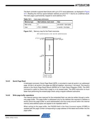
14.5.1 Write/erase page operation
Flash technology requires that an erase must be done before programming. The entire flash can
be erased by an Erase All command. Alternatively, pages can be individually erased by the
Erase Page command.
The User page can be written and erased using the mechanisms described in this chapter.
After programming, the page can be locked to prevent miscellaneous write or erase sequences.
Locking is performed on a per-region basis, so locking a region locks all pages inside the region.
Additional protection is provided for the lowermost address space of the flash. This address
space is allocated for the Boot Loader, and is protected both by the lock bit(s) corresponding to
this address space, and the BOOTPROT[2:0] fuses.
Data to be written are stored in an internal buffer called page buffer. The page buffer contains w
words. The page buffer wraps around within the internal memory area address space and
appears to be repeated by the number of pages in it. Writing of 8-bit and 16-bit data to the page
buffer is not allowed and may lead to unpredictable data corruption.
Data must be written to the page buffer before the programming command is written to FCMD.
The sequence is as follows:
• Reset the page buffer with the Clear Page Buffer command.
• Fill the page buffer with the desired contents, using only 32-bit access.
• Programming starts as soon as the programming key and the programming command are
written to the Flash Command Register. The FCMD.PAGEN field must contain the address of
the page to write. PAGEN is automatically updated when writing to the page buffer, but can
also be written to directly. The FRDY bit in FSR is automatically cleared when the page write
operation starts.
• When programming is completed, the bit FRDY in FSR is set. If an interrupt was enabled by
setting the bit FRDY in FCR, the interrupt line of the flash controller is set.
Two errors can be detected in FSR after a programming sequence:
• Programming Error: A bad keyword and/or an invalid command have been written in FCMD.
• Lock Error: The page to be programmed belongs to a locked region. A command must be
executed to unlock the corresponding region before programming can start.
14.5.2 Erase All operation
The entire memory is erased if the Erase All command (EA) is written to FCMD. Erase All erases
all bits in the flash array. The User page is not erased. All flash memory locations, the general-
purpose fuse bits, and the security bit are erased (reset to 0xFF) after an Erase All.](https://image.slidesharecdn.com/doc32059-150506085255-conversion-gate02/85/Doc32059-124-320.jpg)
![127
32059L–AVR32–01/2012
AT32UC3B
To erase or write a general-purpose fuse bit, the commands Write General-Purpose Fuse Bit
(WGPB) and Erase General-Purpose Fuse Bit (EGPB) are provided. Writing one of these com-
mands, together with the number of the fuse to write/erase, performs the desired operation.
An entire General-Purpose Fuse byte can be written at a time by using the Program GP Fuse
Byte (PGPFB) instruction. A PGPFB to GP fuse byte 2 is not allowed if the flash is locked by the
security bit. The PFB command is issued with a parameter in the PAGEN field:
• PAGEN[2:0] - byte to write
• PAGEN[10:3] - Fuse value to write
All General-Purpose fuses can be erased by the Erase All General-Purpose fuses (EAGP) com-
mand. An EAGP command is not allowed if the flash is locked by the security bit.
Two errors can be detected in FSR after issuing these commands:
• Programming Error: A bad keyword and/or an invalid command have been written in FCMD.
• Lock Error: A write or erase of any of the special-function fuse bits in Table 14-3 was
attempted while the flash is locked by the security bit.
The lock bits are implemented using the lowest 16 general-purpose fuse bits. This means that
the 16 lowest general-purpose fuse bits can also be written/erased using the commands for
locking/unlocking regions, see Section 14.5.3.
14.7 Security bit
The security bit allows the entire chip to be locked from external JTAG or other debug access for
code security. The security bit can be written by a dedicated command, Set Security Bit (SSB).
Once set, the only way to clear the security bit is through the JTAG Chip Erase command.
Once the Security bit is set, the following Flash controller commands will be unavailable and
return a lock error if attempted:
• Write General-Purpose Fuse Bit (WGPB) to BOOTPROT or EPFL fuses
• Erase General-Purpose Fuse Bit (EGPB) to BOOTPROT or EPFL fuses
• Program General-Purpose Fuse Byte (PGPFB) of fuse byte 2
• Erase All General-Purpose Fuses (EAGPF)
One error can be detected in FSR after issuing the command:
• Programming Error: A bad keyword and/or an invalid command have been written in FCMD.](https://image.slidesharecdn.com/doc32059-150506085255-conversion-gate02/85/Doc32059-127-320.jpg)
![130
32059L–AVR32–01/2012
AT32UC3B
14.8.2 Flash Command Register
Name: FCMD
Access Type: Read/Write
Offset: 0x04
Reset value: 0x00000000
FCMD can not be written if the flash is in the process of performing a flash command. Doing so
will cause the FCR write to be ignored, and the PROGE bit to be set.
• CMD: Command
This field defines the flash command. Issuing any unused command will cause the Programming Error bit to be set, and the
corresponding interrupt to be requested if FCR.PROGE is set.
31 30 29 28 27 26 25 24
KEY
23 22 21 20 19 18 17 16
PAGEN [15:8]
15 14 13 12 11 10 9 8
PAGEN [7:0]
7 6 5 4 3 2 1 0
- - CMD
Table 14-5. Set of commands
Command Value Mnemonic
No operation 0 NOP
Write Page 1 WP
Erase Page 2 EP
Clear Page Buffer 3 CPB
Lock region containing given Page 4 LP
Unlock region containing given Page 5 UP
Erase All 6 EA
Write General-Purpose Fuse Bit 7 WGPB
Erase General-Purpose Fuse Bit 8 EGPB
Set Security Bit 9 SSB
Program GP Fuse Byte 10 PGPFB
Erase All GPFuses 11 EAGPF
Quick Page Read 12 QPR](https://image.slidesharecdn.com/doc32059-150506085255-conversion-gate02/85/Doc32059-130-320.jpg)
![131
32059L–AVR32–01/2012
AT32UC3B
• PAGEN: Page number
The PAGEN field is used to address a page or fuse bit for certain operations. In order to simplify programming, the PAGEN field
is automatically updated every time the page buffer is written to. For every page buffer write, the PAGEN field is updated with
the page number of the address being written to. Hardware automatically masks writes to the PAGEN field so that only bits
representing valid page numbers can be written, all other bits in PAGEN are always 0. As an example, in a flash with 1024
pages (page 0 - page 1023), bits 15:10 will always be 0.
• KEY: Write protection key
This field should be written with the value 0xA5 to enable the command defined by the bits of the register. If the field is written
with a different value, the write is not performed and no action is started.
This field always reads as 0.
Write User Page 13 WUP
Erase User Page 14 EUP
Quick Page Read User Page 15 QPRUP
Table 14-6. Semantic of PAGEN field in different commands
Command PAGEN description
No operation Not used
Write Page The number of the page to write
Clear Page Buffer Not used
Lock region containing given Page Page number whose region should be locked
Unlock region containing given Page Page number whose region should be unlocked
Erase All Not used
Write General-Purpose Fuse Bit GPFUSE #
Erase General-Purpose Fuse Bit GPFUSE #
Set Security Bit Not used
Program GP Fuse Byte WriteData[7:0], ByteAddress[2:0]
Erase All GP Fuses Not used
Quick Page Read Page number
Write User Page Not used
Erase User Page Not used
Quick Page Read User Page Not used
Table 14-5. Set of commands
Command Value Mnemonic](https://image.slidesharecdn.com/doc32059-150506085255-conversion-gate02/85/Doc32059-131-320.jpg)
![136
32059L–AVR32–01/2012
AT32UC3B
14.9 Fuses Settings
The flash block contains a number of general purpose fuses. Some of these fuses have defined
meanings outside the flash controller and are described in this section.
The general purpose fuses are erase by a JTAG chip erase.
14.9.1 Flash General Purpose Fuse Register Low (FGPFRLO)
BODEN: Brown Out Detector Enable
BODHYST: Brown Out Detector Hysteresis
0: The Brown out detector hysteresis is disabled
1: The Brown out detector hysteresis is enabled
BODLEVEL: Brown Out Detector Trigger Level
This controls the voltage trigger level for the Brown out detector. Refer to Electrical Characteris-
tics section. If the BODLEVEL is set higher than VDDCORE and enabled byt fuses, the part will
be in constant reset. To recover from this situation, apply an external voltage on VDDCORE that
is higher than the BOD level and disable the BOD.
LOCK, EPFL, BOOTPROT
These are Flash controller fuses and are described in the FLASHC section.
As no external memories can be connected to AT32UC3B the EPFL bit has no effect.
31 30 29 28 27 26 25 24
GPF31 GPF30 GPF29 BODEN BODHYST BODLEVEL[5:4]
23 22 21 20 19 18 17 16
BODLEVEL[3:0] BOOTPROT EPFL
15 14 13 12 11 10 9 8
LOCK[15:8]
7 6 5 4 3 2 1 0
LOCK[7:0]
BODEN Description
0x0 BOD disabled
0x1 BOD enabled, BOD reset enabled
0x2 BOD enabled, BOD reset disabled
0x3 BOD disabled](https://image.slidesharecdn.com/doc32059-150506085255-conversion-gate02/85/Doc32059-136-320.jpg)

![158
32059L–AVR32–01/2012
AT32UC3B
16.6.3 Memory Address Register
Name: MAR
Access Type: Read/Write
Offset: 0x000 + n*0x040
Reset Value: 0x00000000
• MADDR: Memory Address
Address of memory buffer. MADDR should be programmed to point to the start of the memory buffer when configuring the
PDCA. During transfer, MADDR will point to the next memory location to be read/written.
31 30 29 28 27 26 25 24
MADDR[31:24]
23 22 21 20 19 18 17 16
MADDR[23:16]
15 14 13 12 11 10 9 8
MADDR[15:8]
7 6 5 4 3 2 1 0
MADDR[7:0]](https://image.slidesharecdn.com/doc32059-150506085255-conversion-gate02/85/Doc32059-158-320.jpg)
![160
32059L–AVR32–01/2012
AT32UC3B
16.6.5 Transfer Counter Register
Name: TCR
Access Type: Read/Write
Offset: 0x008 + n*0x040
Reset Value: 0x00000000
• TCV: Transfer Counter Value
Number of data items to be transferred by the PDCA. TCV must be programmed with the total number of transfers to be made.
During transfer, TCV contains the number of remaining transfers to be done.
31 30 29 28 27 26 25 24
- - - - - - - -
23 22 21 20 19 18 17 16
- - - - - - - -
15 14 13 12 11 10 9 8
TCV[15:8]
7 6 5 4 3 2 1 0
TCV[7:0]](https://image.slidesharecdn.com/doc32059-150506085255-conversion-gate02/85/Doc32059-160-320.jpg)
![161
32059L–AVR32–01/2012
AT32UC3B
16.6.6 Memory Address Reload Register
Name: MARR
Access Type: Read/Write
Offset: 0x00C + n*0x040
Reset Value: 0x00000000
• MARV: Memory Address Reload Value
Reload Value for the MAR register. This value will be loaded into MAR when TCR reaches zero if the TCRR register has a non-
zero value.
31 30 29 28 27 26 25 24
MARV[31:24]
23 22 21 20 19 18 17 16
MARV[23:16]
15 14 13 12 11 10 9 8
MARV[15:8]
7 6 5 4 3 2 1 0
MARV[7:0]](https://image.slidesharecdn.com/doc32059-150506085255-conversion-gate02/85/Doc32059-161-320.jpg)
![162
32059L–AVR32–01/2012
AT32UC3B
16.6.7 Transfer Counter Reload Register
Name: TCRR
Access Type: Read/Write
Offset: 0x010 + n*0x040
Reset Value: 0x00000000
• TCRV: Transfer Counter Reload Value
Reload value for the TCR register. When TCR reaches zero, it will be reloaded with TCRV if TCRV has a positive value. If TCRV
is zero, no more transfers will be performed for the channel. When TCR is reloaded, the TCRR register is cleared.
31 30 29 28 27 26 25 24
- - - - - - - -
23 22 21 20 19 18 17 16
- - - - - - - -
15 14 13 12 11 10 9 8
TCRV[15:8]
7 6 5 4 3 2 1 0
TCRV[7:0]](https://image.slidesharecdn.com/doc32059-150506085255-conversion-gate02/85/Doc32059-162-320.jpg)


![191
32059L–AVR32–01/2012
AT32UC3B
17.7 Programming Examples
17.7.1 8-bit LED-Chaser
// Set R0 to GPIO base address
mov R0, LO(AVR32_GPIO_ADDRESS)
orh R0, HI(AVR32_GPIO_ADDRESS)
// Enable GPIO control of pin 0-8
mov R1, 0xFF
st.w R0[AVR32_GPIO_GPERS], R1
// Set initial value of port
mov R2, 0x01
st.w R0[AVR32_GPIO_OVRS], R2
// Set up toggle value. Two pins are toggled
// in each round. The bit that is currently set,
// and the next bit to be set.
mov R2, 0x0303
orh R2, 0x0303
loop:
// Only change 8 LSB
mov R3, 0x00FF
and R3, R2
st.w R0[AVR32_GPIO_OVRT], R3
rol R2
rcall delay
rjmp loop
It is assumed in this example that a subroutine "delay" exists that returns after a given time.
17.7.2 Configuration of USART pins
The example below shows how to configure a peripheral module to control I/O pins. It assumed
in this example that the USART receive pin (RXD) is connected to PC16 and that the USART
transmit pin (TXD) is connected to PC17. For both pins, the USART is peripheral B. In this
example, the state of the GPIO registers is assumed to be unknown. The two USART pins are
therefore first set to be controlled by the GPIO with output drivers disabled. The pins can then be
assured to be tri-stated while changing the Peripheral Mux Registers.
// Set up pointer to GPIO, PORTC
mov R0, LO(AVR32_GPIO_ADDRESS + PORTC_OFFSET)
orh R0, HI(AVR32_GPIO_ADDRESS + PORTC_OFFSET)
// Disable output drivers](https://image.slidesharecdn.com/doc32059-150506085255-conversion-gate02/85/Doc32059-191-320.jpg)
![192
32059L–AVR32–01/2012
AT32UC3B
mov R1, 0x0000
orh R1, 0x0003
st.w R0[AVR32_GPIO_ODERC], R1
// Make the GPIO control the pins
st.w R0[AVR32_GPIO_GPERS], R1
// Select peripheral B on PC16-PC17
st.w R0[AVR32_GPIO_PMR0S], R1
st.w R0[AVR32_GPIO_PMR1C], R1
// Enable peripheral control
st.w R0[AVR32_GPIO_GPERC], R1](https://image.slidesharecdn.com/doc32059-150506085255-conversion-gate02/85/Doc32059-192-320.jpg)
![203
32059L–AVR32–01/2012
AT32UC3B
to an interrupt, and thus might lead to difficulties for interfacing with some serial peripherals
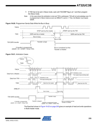
requiring the chip select line to remain active during a full set of transfers.
To facilitate interfacing with such devices, the Chip Select Register can be programmed with the
CSAAT bit (Chip Select Active After Transfer) at 1. This allows the chip select lines to remain in
their current state (low = active) until transfer to another peripheral is required.
Figure 18-8 on page 203 shows different peripheral deselection cases and the effect of the
CSAAT bits.
Figure 18-8. Peripheral Deselection
18.7.3.8 Mode Fault Detection
A mode fault is detected when the SPI is programmed in Master Mode and a low level is driven
by an external master on the NPCS0/NSS signal. NPCS0, MOSI, MISO and SPCK must be con-
figured in open drain through the GPIO controller, so that external pull up resistors are needed to
guarantee high level.
When a mode fault is detected, the MODF bit in the SR is set until the SR is read and the SPI is
automatically disabled until re-enabled by writing the SPIEN bit in the CR (Control Register) at 1.
By default, the Mode Fault detection circuitry is enabled. The user can disable Mode Fault
detection by setting the MODFDIS bit in the SPI Mode Register (MR).
A
NPCS[0..3]
Write SPI_TDR
TDRE
NPCS[0..3]
Write SPI_TDR
TDRE
NPCS[0..3]
Write SPI_TDR
TDRE
DLYBCS
PCS = A
DLYBCS
DLYBCT
A
PCS = B
B
DLYBCS
PCS = A
DLYBCS
DLYBCT
A
PCS = B
B
DLYBCS
DLYBCT
PCS=A
A
DLYBCS
DLYBCT
A
PCS = A
AA
DLYBCT
A A
CSAAT = 0
DLYBCT
A A
CSAAT = 1
A](https://image.slidesharecdn.com/doc32059-150506085255-conversion-gate02/85/Doc32059-203-320.jpg)
![208
32059L–AVR32–01/2012
AT32UC3B
18.8.2 Mode Register
Name: MR
Access Type: Read/Write
Offset: 0x04
Reset Value: 0x00000000
• DLYBCS: Delay Between Chip Selects
This field defines the delay from NPCS inactive to the activation of another NPCS. The DLYBCS time guarantees non-
overlapping chip selects and solves bus contentions in case of peripherals having long data float times.
If DLYBCS is less than or equal to six, six CLK_SPI periods will be inserted by default.
Otherwise, the following equation determines the delay:
• PCS: Peripheral Chip Select
This field is only used if Fixed Peripheral Select is active (PS = 0).
If PCSDEC = 0:
PCS = xxx0NPCS[3:0] = 1110
PCS = xx01NPCS[3:0] = 1101
PCS = x011NPCS[3:0] = 1011
PCS = 0111NPCS[3:0] = 0111
PCS = 1111forbidden (no peripheral is selected)
(x = don’t care)
If PCSDEC = 1:
NPCS[3:0] output signals = PCS.
• LLB: Local Loopback Enable
0: Local loopback path disabled.
1: Local loopback path enabled (
LLB controls the local loopback on the data serializer for testing in Master Mode only. (MISO is internally connected on MOSI.)
• MODFDIS: Mode Fault Detection
0: Mode fault detection is enabled.
1: Mode fault detection is disabled.
• PCSDEC: Chip Select Decode
0: The chip selects are directly connected to a peripheral device.
1: The four chip select lines are connected to a 4- to 16-bit decoder.
When PCSDEC equals one, up to 15 Chip Select signals can be generated with the four lines using an external 4- to 16-bit
decoder. The Chip Select Registers define the characteristics of the 15 chip selects according to the following rules:
CSR0 defines peripheral chip select signals 0 to 3.
CSR1 defines peripheral chip select signals 4 to 7.
CSR2 defines peripheral chip select signals 8 to 11.
31 30 29 28 27 26 25 24
DLYBCS
23 22 21 20 19 18 17 16
– – – – PCS
15 14 13 12 11 10 9 8
– – – – – – – –
7 6 5 4 3 2 1 0
LLB - - MODFDIS – PCSDEC PS MSTR
Delay Between Chip Selects
DLYBCS
CLKSPI
-----------------------=](https://image.slidesharecdn.com/doc32059-150506085255-conversion-gate02/85/Doc32059-208-320.jpg)
![211
32059L–AVR32–01/2012
AT32UC3B
18.8.4 Transmit Data Register
Name: TDR
Access Type: Write-only
Offset: 0x0C
Reset Value: 0x00000000
• LASTXFER: Last Transfer
0: No effect.
1: The current NPCS will be deasserted after the character written in TD has been transferred. When CSAAT is set, this allows
to close the communication with the current serial peripheral by raising the corresponding NPCS line as soon as TD transfer has
completed.
This field is only used if Variable Peripheral Select is active (PS = 1).
• PCS: Peripheral Chip Select
This field is only used if Variable Peripheral Select is active (PS = 1).
If PCSDEC = 0:
PCS = xxx0NPCS[3:0] = 1110
PCS = xx01NPCS[3:0] = 1101
PCS = x011NPCS[3:0] = 1011
PCS = 0111NPCS[3:0] = 0111
PCS = 1111forbidden (no peripheral is selected)
(x = don’t care)
If PCSDEC = 1:
NPCS[3:0] output signals = PCS
• TD: Transmit Data
Data to be transmitted by the SPI Interface is stored in this register. Information to be transmitted must be written to the
transmit data register in a right-justified format.
31 30 29 28 27 26 25 24
– – – – – – – LASTXFER
23 22 21 20 19 18 17 16
– – – – PCS
15 14 13 12 11 10 9 8
TD
7 6 5 4 3 2 1 0
TD](https://image.slidesharecdn.com/doc32059-150506085255-conversion-gate02/85/Doc32059-211-320.jpg)

![226
32059L–AVR32–01/2012
AT32UC3B
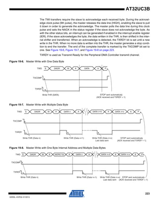
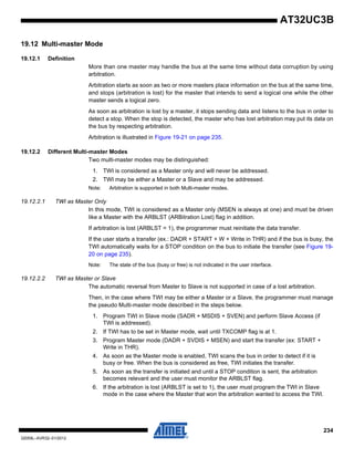
Figure 19-12. Master Read with One, Two or Three Bytes Internal Address and One Data Byte
19.10.7.2 10-bit Slave Addressing
For a slave address higher than 7 bits, the user must configure the address size (IADRSZ) and
set the other slave address bits in the internal address register (IADR). The two remaining Inter-
nal address bytes, IADR[15:8] and IADR[23:16] can be used the same as in 7-bit Slave
Addressing.
Example: Address a 10-bit device:
(10-bit device address is b1 b2 b3 b4 b5 b6 b7 b8 b9 b10)
1. Program IADRSZ = 1,
2. Program DADR with 1 1 1 1 0 b1 b2 (b1 is the MSB of the 10-bit address, b2, etc.)
3. Program IADR with b3 b4 b5 b6 b7 b8 b9 b10 (b10 is the LSB of the 10-bit address)
Figure 19-13 below shows a byte write to an Atmel AT24LC512 EEPROM. This demonstrates
the use of internal addresses to access the device.
Figure 19-13. Internal Address Usage
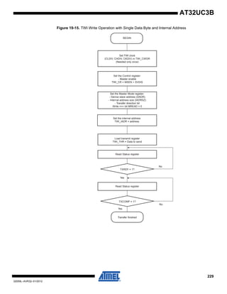
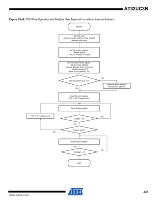
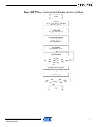
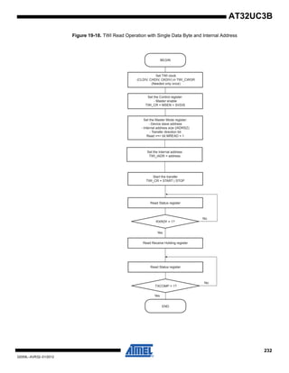
19.11 Using the Peripheral DMA Controller
The use of the Peripheral DMA Controller significantly reduces the CPU load.
S DADR W A IADR(23:16) A IADR(15:8) A IADR(7:0) A
S DADR W A IADR(15:8) A IADR(7:0) A
A IADR(7:0) AS DADR W
DATA N P
Sr DADR R A
Sr DADR R A DATA N P
Sr DADR R A DATA N P
TWD
TWD
TWD
Three bytes internal address
Two bytes internal address
One byte internal address
S
T
A
R
T
M
S
B
Device
Address
0
L
S
B
R
/
W
A
C
K
M
S
B
W
R
I
T
E
A
C
K
A
C
K
L
S
B
A
C
K
FIRST
WORD ADDRESS
SECOND
WORD ADDRESS DATA
S
T
O
P](https://image.slidesharecdn.com/doc32059-150506085255-conversion-gate02/85/Doc32059-226-320.jpg)
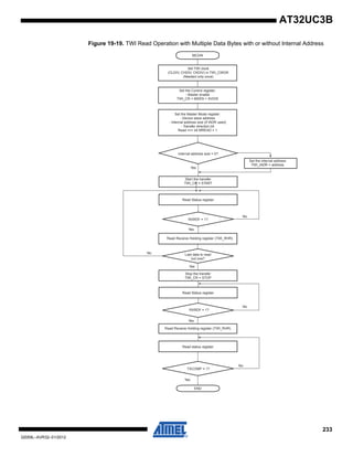
![248
32059L–AVR32–01/2012
AT32UC3B
19.14.2 Master Mode Register
Name: MMR
Access: Read-write
Offset: 0x04
Reset Value: 0x00000000
• DADR: Device Address
The device address is used to access slave devices in read or write mode. Those bits are only used in Master mode.
• MREAD: Master Read Direction
0 = Master write direction.
1 = Master read direction.
• IADRSZ: Internal Device Address Size
31 30 29 28 27 26 25 24
– – – – – – – –
23 22 21 20 19 18 17 16
– DADR
15 14 13 12 11 10 9 8
– – – MREAD – – IADRSZ
7 6 5 4 3 2 1 0
– – – – – – – –
IADRSZ[9:8] Description
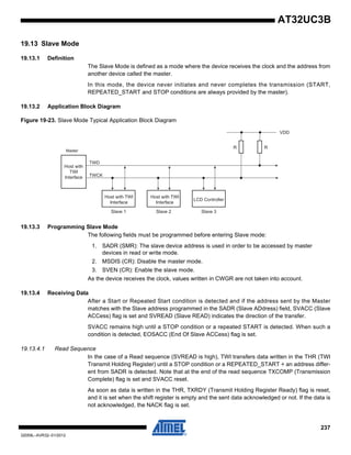
0 0 No internal device address
0 1 One-byte internal device address
1 0 Two-byte internal device address
1 1 Three-byte internal device address](https://image.slidesharecdn.com/doc32059-150506085255-conversion-gate02/85/Doc32059-248-320.jpg)


![277
32059L–AVR32–01/2012
AT32UC3B
20.9.2 Clock Mode Register
Name: CMR
Access Type: Read/Write
Offset: 0x04
Reset value: 0x00000000
• DIV[11:0]: Clock Divider
The divided clock equals the CLK_SSC divided by two times DIV. The maximum bit rate is CLK_SSC/2. The minimum bit rate is
CLK_SSC/(2 x 4095) = CLK_SSC/8190.
The clock divider is not active when DIV equals zero.
31 30 29 28 27 26 25 24
- - - - - - - -
23 22 21 20 19 18 17 16
- - - - - - - -
15 14 13 12 11 10 9 8
- - - - DIV[11:8]
7 6 5 4 3 2 1 0
DIV[7:0]
Divided Clock CLK_SSC (⁄ DIV 2)×=](https://image.slidesharecdn.com/doc32059-150506085255-conversion-gate02/85/Doc32059-277-320.jpg)
![286
32059L–AVR32–01/2012
AT32UC3B
20.9.7 Receive Holding Register
Name: RHR
Access Type: Read-only
Offset: 0x20
Reset value: 0x00000000
• RDAT: Receive Data
Right aligned regardless of the number of data bits defined by the RFMR.DATLEN field.
31 30 29 28 27 26 25 24
RDAT[31:24]
23 22 21 20 19 18 17 16
RDAT[23:16]
15 14 13 12 11 10 9 8
RDAT[15:8]
7 6 5 4 3 2 1 0
RDAT[7:0]](https://image.slidesharecdn.com/doc32059-150506085255-conversion-gate02/85/Doc32059-286-320.jpg)
![287
32059L–AVR32–01/2012
AT32UC3B
20.9.8 Transmit Holding Register
Name: THR
Access Type: Write-only
Offset: 0x24
Reset value: 0x00000000
• TDAT: Transmit Data
Right aligned regardless of the number of data bits defined by the TFMR.DATLEN field.
31 30 29 28 27 26 25 24
TDAT[31:24]
23 22 21 20 19 18 17 16
TDAT[23:16]
15 14 13 12 11 10 9 8
TDAT[15:8]
7 6 5 4 3 2 1 0
TDAT[7:0]](https://image.slidesharecdn.com/doc32059-150506085255-conversion-gate02/85/Doc32059-287-320.jpg)
![288
32059L–AVR32–01/2012
AT32UC3B
20.9.9 Receive Synchronization Holding Register
Name: RSHR
Access Type: Read-only
Offset: 0x30
Reset value: 0x00000000
• RSDAT: Receive Synchronization Data
31 30 29 28 27 26 25 24
- - - - - - - -
23 22 21 20 19 18 17 16
- - - - - - - -
15 14 13 12 11 10 9 8
RSDAT[15:8]
7 6 5 4 3 2 1 0
RSDAT[7:0]](https://image.slidesharecdn.com/doc32059-150506085255-conversion-gate02/85/Doc32059-288-320.jpg)
![289
32059L–AVR32–01/2012
AT32UC3B
20.9.10 Transmit Synchronization Holding Register
Name: TSHR
Access Type: Read/Write
Offset: 0x34
Reset value: 0x00000000
• TSDAT: Transmit Synchronization Data
31 30 29 28 27 26 25 24
- - - - - - - -
23 22 21 20 19 18 17 16
- - - - - - - -
15 14 13 12 11 10 9 8
TSDAT[15:8]
7 6 5 4 3 2 1 0
TSDAT[7:0]](https://image.slidesharecdn.com/doc32059-150506085255-conversion-gate02/85/Doc32059-289-320.jpg)
![290
32059L–AVR32–01/2012
AT32UC3B
20.9.11 Receive Compare 0 Register
Name: RC0R
Access Type: Read/Write
Offset: 0x38
Reset value: 0x00000000
• CP0: Receive Compare Data 0
31 30 29 28 27 26 25 24
- - - - - - - -
23 22 21 20 19 18 17 16
- - - - - - - -
15 14 13 12 11 10 9 8
CP0[15:8]
7 6 5 4 3 2 1 0
CP0[7:0]](https://image.slidesharecdn.com/doc32059-150506085255-conversion-gate02/85/Doc32059-290-320.jpg)
![291
32059L–AVR32–01/2012
AT32UC3B
20.9.12 Receive Compare 1 Register
Name: RC1R
Access Type: Read/Write
Offset: 0x3C
Reset value: 0x00000000
• CP1: Receive Compare Data 1
31 30 29 28 27 26 25 24
- - - - - - - -
23 22 21 20 19 18 17 16
- - - - - - - -
15 14 13 12 11 10 9 8
CP1[[15:8]
7 6 5 4 3 2 1 0
CP1[7:0]](https://image.slidesharecdn.com/doc32059-150506085255-conversion-gate02/85/Doc32059-291-320.jpg)


![311
32059L–AVR32–01/2012
AT32UC3B
Figure 21-18. FSK Modulator Output
21.6.4.6 Synchronous Receiver
In synchronous mode (SYNC=1), the receiver samples the RXD signal on each rising edge of
the Baud Rate Clock. If a low level is detected, it is considered as a start bit. Configuration bits
and fields are the same as in asynchronous mode.
Figure 21-19. Synchronous Mode Character Reception
21.6.4.7 Receiver Operations
When a character reception is completed, it is transferred to the Received Character field in the
Receive Holding Register (RHR.RXCHR), and the Receiver Ready bit in the Channel Status
Register (CSR.RXRDY) is set. If RXRDY is already set, RHR will be overwritten and the Overrun
Error bit (CSR.OVRE) is set. Reading RHR will clear CSR.RXRDY, and writing a one to the
Reset Status bit in the Control Register (CR.RSTSTA) will clear CSR.OVRE.
Manchester
encoded
data
default polarity
unipolar output
Txd
FSK Modulator
Output
Uptstream Frequencies
[F0, F0+offset]
NRZ stream
1 0 0 1
D0 D1 D2 D3 D4 D5 D6 D7
RXD
Start
Sampling
Parity Bit
Stop Bit
Example: 8-bit, Parity Enabled 1 Stop
Baud Rate
Clock](https://image.slidesharecdn.com/doc32059-150506085255-conversion-gate02/85/Doc32059-311-320.jpg)
![339
32059L–AVR32–01/2012
AT32UC3B
21.7.7 Receiver Holding Register
Name: RHR
Access Type: Read-only
Offset: 0x18
Reset Value: 0x00000000
Reading this register will clear the CSR.RXRDY bit.
• RXSYNH: Received Sync
0: Last character received is a data sync.
1: Last character received is a command sync.
• RXCHR: Received Character
Last received character.
31 30 29 28 27 26 25 24
– – – – – – – –
23 22 21 20 19 18 17 16
– – – – – – – –
15 14 13 12 11 10 9 8
RXSYNH – – – – – – RXCHR[8]
7 6 5 4 3 2 1 0
RXCHR[7:0]](https://image.slidesharecdn.com/doc32059-150506085255-conversion-gate02/85/Doc32059-339-320.jpg)
![340
32059L–AVR32–01/2012
AT32UC3B
21.7.8 Transmitter Holding Register
Name: THR
Access Type: Write-only
Offset: 0x1C
Reset Value: 0x00000000
• TXSYNH: Sync Field to be transmitted
0: If MR.VARSYNC is a one, the next character sent is encoded as data, and the start frame delimiter is a data sync.
1: If MR.VARSYNC is a one, the next character sent is encoded as a command, and the start frame delimiter is a command
sync.
• TXCHR: Character to be Transmitted
If TXRDY is zero this field contains the next character to be transmitted.
31 30 29 28 27 26 25 24
– – – – – – – –
23 22 21 20 19 18 17 16
– – – – – – – –
15 14 13 12 11 10 9 8
TXSYNH – – – – – – TXCHR[8]
7 6 5 4 3 2 1 0
TXCHR[7:0]](https://image.slidesharecdn.com/doc32059-150506085255-conversion-gate02/85/Doc32059-340-320.jpg)
![341
32059L–AVR32–01/2012
AT32UC3B
21.7.9 Baud Rate Generator Register
Name: BRGR
Access Type: Read-write
Offset: 0x20
Reset Value: 0x00000000
• FP: Fractional Part
0: Fractional divider is disabled.
1 - 7: Baud rate resolution, defined by FP x 1/8.
• CD: Clock Divider
31 30 29 28 27 26 25 24
– – – – – – – –
23 22 21 20 19 18 17 16
– – – – – FP
15 14 13 12 11 10 9 8
CD[15:8]
7 6 5 4 3 2 1 0
CD[7:0]
Table 21-21. Baud Rate in Asynchronous Mode (MR.SYNC is 0)
CD OVER = 0 OVER = 1
0 Baud Rate Clock Disabled
1 to 65535
Table 21-22. Baud Rate in Synchronous Mode (MR.SYNC is 1) and SPI Mode
CD Baud Rate
0 Baud Rate Clock Disabled
1 to 65535
Baud Rate
Selected Clock
16 CD⋅
----------------------------------------= Baud Rate
Selected Clock
8 CD⋅
----------------------------------------=
Baud Rate
Selected Clock
CD
----------------------------------------=](https://image.slidesharecdn.com/doc32059-150506085255-conversion-gate02/85/Doc32059-341-320.jpg)
![343
32059L–AVR32–01/2012
AT32UC3B
21.7.10 Receiver Time-out Register
Name: RTOR
Access Type: Read-write
Offset: 0x24
Reset Value: 0x00000000
• TO: Time-out Value
0: The receiver Time-out is disabled.
1 - 65535: The receiver Time-out is enabled and the time-out delay is TO x bit period.
Note that the size of the TO counter is device dependent, see the Module Configuration section.
31 30 29 28 27 26 25 24
– – – – – – – –
23 22 21 20 19 18 17 16
– – – – – – – –
15 14 13 12 11 10 9 8
TO[15:8]
7 6 5 4 3 2 1 0
TO[7:0]](https://image.slidesharecdn.com/doc32059-150506085255-conversion-gate02/85/Doc32059-343-320.jpg)
![345
32059L–AVR32–01/2012
AT32UC3B
21.7.12 FI DI Ratio Register
Name: FIDI
Access Type: Read-write
Offset: 0x40
Reset Value: 0x00000174
• FI_DI_RATIO: FI Over DI Ratio Value
0: If ISO7816 mode is selected, the baud rate generator does not generate a signal.
1 - 2047: If ISO7816 mode is selected, the baud rate is the clock provided on CLK divided by FI_DI_RATIO.
31 30 29 28 27 26 25 24
– – – – – – – –
23 22 21 20 19 18 17 16
– – – – – – – –
15 14 13 12 11 10 9 8
– – – – – FI_DI_RATIO[10:8]
7 6 5 4 3 2 1 0
FI_DI_RATIO[7:0]](https://image.slidesharecdn.com/doc32059-150506085255-conversion-gate02/85/Doc32059-345-320.jpg)

![350
32059L–AVR32–01/2012
AT32UC3B
21.7.16 Version Register
Name: VERSION
Access Type: Read-only
Offset: 0xFC
Reset Value: -
• MFN
Reserved. No functionality associated.
• VERSION
Version of the module. No functionality associated.
31 30 29 28 27 26 25 24
– – – – – – – –
23 22 21 20 19 18 17 16
– – – – MFN
15 14 13 12 11 10 9 8
– – – – VERSION[11:8]
7 6 5 4 3 2 1 0
VERSION[7:0]](https://image.slidesharecdn.com/doc32059-150506085255-conversion-gate02/85/Doc32059-350-320.jpg)

![406
32059L–AVR32–01/2012
AT32UC3B
22.8.1.5 Version Register
Register Name: UVERS
Access Type: Read-Only
Offset: 0x0818
Read Value: -
• VARIANT: Variant Number
Reserved. No functionality associated.
• VERSION: Version Number
Version number of the module. No functionality associated.
31 30 29 28 27 26 25 24
- - - - - - - -
23 22 21 20 19 18 17 16
- - - - VARIANT
15 14 13 12 11 10 9 8
- - - - VERSION[11:8]
7 6 5 4 3 2 1 0
VERSION[7:0]](https://image.slidesharecdn.com/doc32059-150506085255-conversion-gate02/85/Doc32059-406-320.jpg)
![409
32059L–AVR32–01/2012
AT32UC3B
22.8.1.7 Address Size Register
Register Name: UADDRSIZE
Access Type: Read-Only
Offset: 0x0820
Read Value: -
• UADDRSIZE: IP PB Address Size
This field indicates the size of the PB address space reserved for the USBB IP interface.
31 30 29 28 27 26 25 24
UADDRSIZE[31:24]
23 22 21 20 19 18 17 16
UADDRSIZE[23:16]
15 14 13 12 11 10 9 8
UADDRSIZE[15:8]
7 6 5 4 3 2 1 0
UADDRSIZE[7:0]](https://image.slidesharecdn.com/doc32059-150506085255-conversion-gate02/85/Doc32059-409-320.jpg)
![410
32059L–AVR32–01/2012
AT32UC3B
22.8.1.8 Name Register 1
Register Name: UNAME1
Access Type: Read-Only
Offset: 0x0824
Read Value: -
• UNAME1: IP Name Part One
This field indicates the first part of the ASCII-encoded name of the USBB IP.
31 30 29 28 27 26 25 24
UNAME1[31:24]
23 22 21 20 19 18 17 16
UNAME1[23:16]
15 14 13 12 11 10 9 8
UNAME1[15:8]
7 6 5 4 3 2 1 0
UNAME1[7:0]](https://image.slidesharecdn.com/doc32059-150506085255-conversion-gate02/85/Doc32059-410-320.jpg)
![411
32059L–AVR32–01/2012
AT32UC3B
22.8.1.9 Name Register 2
Register Name: UNAME2
Access Type: Read-Only
Offset: 0x0828
Read Value:
• UNAME2: IP Name Part Two
This field indicates the second part of the ASCII-encoded name of the USBB IP.
31 30 29 28 27 26 25 24
UNAME2[31:24]
23 22 21 20 19 18 17 16
UNAME2[23:16]
15 14 13 12 11 10 9 8
UNAME2[15:8]
7 6 5 4 3 2 1 0
UNAME2[7:0]](https://image.slidesharecdn.com/doc32059-150506085255-conversion-gate02/85/Doc32059-411-320.jpg)


![423
32059L–AVR32–01/2012
AT32UC3B
22.8.2.9 Device Frame Number Register
Register Name: UDFNUM
Access Type: Read-Only
Offset: 0x0020
Reset Value: 0x00000000
• FNCERR: Frame Number CRC Error
This bit is set when a corrupted frame number is received. This bit and the SOF interrupt bit are updated at the same time.
This bit is cleared upon receiving a USB reset.
• FNUM: Frame Number
This field contains the 11-bit frame number information. It is provided in the last received SOF packet.
This field is cleared upon receiving a USB reset.
FNUM is updated even if a corrupted SOF is received.
31 30 29 28 27 26 25 24
- - - - - - - -
23 22 21 20 19 18 17 16
- - - - - - - -
15 14 13 12 11 10 9 8
FNCERR - FNUM[10:5]
7 6 5 4 3 2 1 0
FNUM[4:0] - - -](https://image.slidesharecdn.com/doc32059-150506085255-conversion-gate02/85/Doc32059-423-320.jpg)
![424
32059L–AVR32–01/2012
AT32UC3B
22.8.2.10 Endpoint n Configuration Register
Register Name: UECFGn, n in [0..6]
Access Type: Read/Write
Offset: 0x0100 + (n * 0x04)
Reset Value: 0x00000000
• EPTYPE: Endpoint Type
This field shall be written to select the endpoint type:
This field is cleared upon receiving a USB reset.
• AUTOSW: Automatic Switch
This bit is cleared upon receiving a USB reset.
1: The automatic bank switching is enabled.
0: The automatic bank switching is disabled.
• EPDIR: Endpoint Direction
This bit is cleared upon receiving a USB reset.
1: The endpoint direction is IN (nor for control endpoints).
0: The endpoint direction is OUT.
31 30 29 28 27 26 25 24
- - - - - - - -
23 22 21 20 19 18 17 16
- - - - - - - -
15 14 13 12 11 10 9 8
- - - EPTYPE - AUTOSW EPDIR
7 6 5 4 3 2 1 0
- EPSIZE EPBK ALLOC -
EPTYPE Endpoint Type
0 0 Control
0 1 Isochronous
1 0 Bulk
1 1 Interrupt](https://image.slidesharecdn.com/doc32059-150506085255-conversion-gate02/85/Doc32059-424-320.jpg)
![426
32059L–AVR32–01/2012
AT32UC3B
22.8.2.11 Endpoint n Status Register
Register Name: UESTAn, n in [0..6]
Access Type: Read-Only 0x0100
Offset: 0x0130 + (n * 0x04)
Reset Value: 0x00000100
• BYCT: Byte Count
This field is set with the byte count of the FIFO.
For IN endpoints, incremented after each byte written by the software into the endpoint and decremented after each byte sent to
the host.
For OUT endpoints, incremented after each byte received from the host and decremented after each byte read by the software
from the endpoint.
This field may be updated one clock cycle after the RWALL bit changes, so the user should not poll this field as an interrupt bit.
• CFGOK: Configuration OK Status
This bit is updated when the ALLOC bit is written to one.
This bit is set if the endpoint n number of banks (EPBK) and size (EPSIZE) are correct compared to the maximal allowed
number of banks and size for this endpoint and to the maximal FIFO size (i.e. the DPRAM size).
If this bit is cleared, the user shall rewrite correct values to the EPBK and EPSIZE fields in the UECFGn register.
• CTRLDIR: Control Direction
This bit is set after a SETUP packet to indicate that the following packet is an IN packet.
This bit is cleared after a SETUP packet to indicate that the following packet is an OUT packet.
Writing a zero or a one to this bit has no effect.
• RWALL: Read/Write Allowed
This bit is set for IN endpoints when the current bank is not full, i.e., the user can write further data into the FIFO.
This bit is set for OUT endpoints when the current bank is not empty, i.e., the user can read further data from the FIFO.
This bit is never set if STALLRQ is one or in case of error.
This bit is cleared otherwise.
This bit shall not be used for control endpoints.
31 30 29 28 27 26 25 24
- BYCT
23 22 21 20 19 18 17 16
BYCT - CFGOK CTRLDIR RWALL
15 14 13 12 11 10 9 8
CURRBK NBUSYBK - - DTSEQ
7 6 5 4 3 2 1 0
SHORT
PACKET
STALLEDI/
CRCERRI
OVERFI NAKINI NAKOUTI
RXSTPI/
UNDERFI
RXOUTI TXINI](https://image.slidesharecdn.com/doc32059-150506085255-conversion-gate02/85/Doc32059-426-320.jpg)
![430
32059L–AVR32–01/2012
AT32UC3B
22.8.2.12 Endpoint n Status Clear Register
Register Name: UESTAnCLR, n in [0..6]
Access Type: Write-Only
Offset: 0x0160 + (n * 0x04)
Read Value: 0x00000000
Writing a one to a bit in this register will clear the corresponding bit in UESTA.
Writing a zero to a bit in this register has no effect.
This bit always reads as zero.
31 30 29 28 27 26 25 24
- - - - - - - -
23 22 21 20 19 18 17 16
- - - - - - - -
15 14 13 12 11 10 9 8
- - - - - - - -
7 6 5 4 3 2 1 0
SHORT
PACKETC
STALLEDIC/
CRCERRIC
OVERFIC NAKINIC NAKOUTIC
RXSTPIC/
UNDERFIC
RXOUTIC TXINIC](https://image.slidesharecdn.com/doc32059-150506085255-conversion-gate02/85/Doc32059-430-320.jpg)
![431
32059L–AVR32–01/2012
AT32UC3B
22.8.2.13 Endpoint n Status Set Register
Register Name: UESTAnSET, n in [0..6]
Access Type: Write-Only
Offset: 0x0190 + (n * 0x04)
Read Value: 0x00000000
Writing a one to a bit in this register will set the corresponding bit in UESTA, what may be useful for test or debug purposes.
Writing a zero to a bit in this register has no effect.
This bit always reads as zero.
31 30 29 28 27 26 25 24
- - - - - - - -
23 22 21 20 19 18 17 16
- - - - - - - -
15 14 13 12 11 10 9 8
- - - NBUSYBKS - - -
7 6 5 4 3 2 1 0
SHORT
PACKETS
STALLEDIS/
CRCERRIS
OVERFIS NAKINIS NAKOUTIS
RXSTPIS/
UNDERFIS
RXOUTIS TXINIS](https://image.slidesharecdn.com/doc32059-150506085255-conversion-gate02/85/Doc32059-431-320.jpg)
![432
32059L–AVR32–01/2012
AT32UC3B
22.8.2.14 Endpoint n Control Register
Register Name: UECONn, n in [0..6]
Access Type: Read-Only
Offset: 0x01C0 + (n * 0x04)
Reset Value: 0x00000000
• STALLRQ: STALL Request
This bit is set when the STALLRQS bit is written to one. This will request to send a STALL handshake to the host.
This bit is cleared when a new SETUP packet is received or when the STALLRQC bit is written to zero.
• RSTDT: Reset Data Toggle
This bit is set when the RSTDTS bit is written to one. This will clear the data toggle sequence, i.e., set to Data0 the data toggle
sequence of the next sent (IN endpoints) or received (OUT endpoints) packet.
This bit is cleared instantaneously.
The user does not have to wait for this bit to be cleared.
• EPDISHDMA: Endpoint Interrupts Disable HDMA Request Enable
This bit is set when the EPDISHDMAS is written to one. This will pause the on-going DMA channel n transfer on any Endpoint n
interrupt (EPnINT), whatever the state of the Endpoint n Interrupt Enable bit (EPnINTE).
The user then has to acknowledge or to disable the interrupt source (e.g. RXOUTI) or to clear the EPDISHDMA bit (by writing a
one to the EPDISHDMAC bit) in order to complete the DMA transfer.
In ping-pong mode, if the interrupt is associated to a new system-bank packet (e.g. Bank1) and the current DMA transfer is
running on the previous packet (Bank0), then the previous-packet DMA transfer completes normally, but the new-packet DMA
transfer will not start (not requested).
If the interrupt is not associated to a new system-bank packet (NAKINI, NAKOUTI, etc.), then the request cancellation may
occur at any time and may immediately pause the current DMA transfer.
This may be used for example to identify erroneous packets, to prevent them from being transferred into a buffer, to complete a
DMA transfer by software after reception of a short packet, etc.
• FIFOCON: FIFO Control
For control endpoints:
The FIFOCON and RWALL bits are irrelevant. The software shall therefore never use them on these endpoints. When read,
their value is always 0.
For IN endpoints:
This bit is set when the current bank is free, at the same time as TXINI.
31 30 29 28 27 26 25 24
- - - - - - - -
23 22 21 20 19 18 17 16
- - - - STALLRQ RSTDT - EPDISHDMA
15 14 13 12 11 10 9 8
- FIFOCON KILLBK NBUSYBKE - - - -
7 6 5 4 3 2 1 0
SHORT
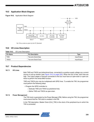
PACKETE
STALLEDE/
CRCERRE
OVERFE NAKINE NAKOUTE
RXSTPE/
UNDERFE
RXOUTE TXINE](https://image.slidesharecdn.com/doc32059-150506085255-conversion-gate02/85/Doc32059-432-320.jpg)
![434
32059L–AVR32–01/2012
AT32UC3B
22.8.2.15 Endpoint n Control Clear Register
Register Name: UECONnCLR, n in [0..6]
Access Type: Write-Only
Offset: 0x0220 + (n * 0x04)
Read Value: 0x00000000
Writing a one to a bit in this register will clear the corresponding bit in UECONn.
Writing a zero to a bit in this register has no effect.
This bit always reads as zero.
31 30 29 28 27 26 25 24
- - - - - - - -
23 22 21 20 19 18 17 16
- - - - STALLRQC - - EPDISHDMAC
15 14 13 12 11 10 9 8
- FIFOCONC - NBUSYBKEC - - - -
7 6 5 4 3 2 1 0
SHORT
PACKETEC
STALLEDEC
/CRCERREC
OVERFEC NAKINEC NAKOUTEC
RXSTPEC/
UNDERFEC
RXOUTEC TXINEC](https://image.slidesharecdn.com/doc32059-150506085255-conversion-gate02/85/Doc32059-434-320.jpg)
![435
32059L–AVR32–01/2012
AT32UC3B
22.8.2.16 Endpoint n Control Set Register
Register Name: UECONnSET, n in [0..6]
Access Type: Write-Only
Offset: 0x01F0 + (n * 0x04)
Read Value: 0x00000000
Writing a one to a bit in this register will set the corresponding bit in UECONn.
Writing a zero to a bit in this register has no effect.
This bit always reads as zero.
31 30 29 28 27 26 25 24
- - - - - - - -
23 22 21 20 19 18 17 16
- - - - STALLRQS RSTDTS - EPDISHDMAS
15 14 13 12 11 10 9 8
- - KILLBKS NBUSYBKES - - - -
7 6 5 4 3 2 1 0
SHORT
PACKETES
STALLEDES/
CRCERRES
OVERFES NAKINES NAKOUTES
RXSTPES/
UNDERFES
RXOUTES TXINES](https://image.slidesharecdn.com/doc32059-150506085255-conversion-gate02/85/Doc32059-435-320.jpg)
![436
32059L–AVR32–01/2012
AT32UC3B
22.8.2.17 Device DMA Channel n Next Descriptor Address Register
Register Name: UDDMAnNEXTDESC, n in [1..6]
Access Type: Read/Write
Offset: 0x0310 + (n - 1) * 0x10
Reset Value: 0x00000000
• NXTDESCADDR: Next Descriptor Address
This field contains the bits 31:4 of the 16-byte aligned address of the next channel descriptor to be processed.
This field is written either or by descriptor loading.
31 30 29 28 27 26 25 24
NXTDESCADDR[31:24]
23 22 21 20 19 18 17 16
NXTDESCADDR[23:16]
15 14 13 12 11 10 9 8
NXTDESCADDR[15:8]
7 6 5 4 3 2 1 0
NXTDESCADDR[7:4] - - - -](https://image.slidesharecdn.com/doc32059-150506085255-conversion-gate02/85/Doc32059-436-320.jpg)
![437
32059L–AVR32–01/2012
AT32UC3B
22.8.2.18 Device DMA Channel n HSB Address Register
Register Name: UDDMAnADDR, n in [1..6]
Access Type: Read/Write
Offset: 0x0314 + (n - 1) * 0x10
Reset Value: 0x00000000
• HSBADDR: HSB Address
This field determines the HSB bus current address of a channel transfer.
The address written to the HSB address bus is HSBADDR rounded down to the nearest word-aligned address, i.e.,
HSBADDR[1:0] is considered as 0b00 since only word accesses are performed.
Channel HSB start and end addresses may be aligned on any byte boundary.
The user may write this field only when the Channel Enabled bit (CHEN) of the UDDMAnSTATUS register is cleared.
This field is updated at the end of the address phase of the current access to the HSB bus. It is incremented of the HSB access
byte-width.
The HSB access width is 4 bytes, or less at packet start or end if the start or end address is not aligned on a word boundary.
The packet start address is either the channel start address or the next channel address to be accessed in the channel buffer.
The packet end address is either the channel end address or the latest channel address accessed in the channel buffer.
The channel start address is written or loaded from the descriptor, whereas the channel end address is either determined by the
end of buffer or the end of USB transfer if the Buffer Close Input Enable bit (BUFFCLOSEINEN) is set.
31 30 29 28 27 26 25 24
HSBADDR[31:24]
23 22 21 20 19 18 17 16
HSBADDR[23:16]
15 14 13 12 11 10 9 8
HSBADDR[15:8]
7 6 5 4 3 2 1 0
HSBADDR[7:0]](https://image.slidesharecdn.com/doc32059-150506085255-conversion-gate02/85/Doc32059-437-320.jpg)
![438
32059L–AVR32–01/2012
AT32UC3B
22.8.2.19 Device DMA Channel n Control Register
Register Name: UDDMAnCONTROL, n in [1..6]
Access Type: Read/Write
Offset: 0x0318 + (n - 1) * 0x10
Reset Value: 0x00000000
• CHBYTELENGTH: Channel Byte Length
This field determines the total number of bytes to be transferred for this buffer.
The maximum channel transfer size 64kB is reached when this field is zero (default value).
If the transfer size is unknown, the transfer end is controlled by the peripheral and this field should be written to zero.
This field can be written or descriptor loading only after the UDDMAnSTATUS.CHEN bit has been cleared, otherwise this field is
ignored.
• BURSTLOCKEN: Burst Lock Enable
1: The USB data burst is locked for maximum optimization of HSB busses bandwidth usage and maximization of fly-by duration.
0: The DMA never locks the HSB access.
• DESCLDIRQEN: Descriptor Loaded Interrupt Enable
1: The Descriptor Loaded interrupt is enabled.This interrupt is generated when a Descriptor has been loaded from the system
bus.
0: The Descriptor Loaded interrupt is disabled.
• EOBUFFIRQEN: End of Buffer Interrupt Enable
1: The end of buffer interrupt is enabled.This interrupt is generated when the channel byte count reaches zero.
0: The end of buffer interrupt is disabled.
• EOTIRQEN: End of USB Transfer Interrupt Enable
1: The end of usb OUT data transfer interrupt is enabled. This interrupt is generated only if the BUFFCLOSEINEN bit is set.
0: The end of usb OUT data transfer interrupt is disabled.
• DMAENDEN: End of DMA Buffer Output Enable
Writing a one to this bit will properly complete the usb transfer at the end of the dma transfer.
For IN endpoint, it means that a short packet (but not a Zero Length Packet) will be sent to the USB line to properly closed the
usb transfer at the end of the dma transfer.
For OUT endpoint, it means that all the banks will be properly released. (NBUSYBK=0) at the end of the dma transfer.
31 30 29 28 27 26 25 24
CHBYTELENGTH[15:8]
23 22 21 20 19 18 17 16
CHBYTELENGTH[7:0]
15 14 13 12 11 10 9 8
- - - - - - - -
7 6 5 4 3 2 1 0
BURSTLOCKEN DESCLDIRQEN EOBUFFIRQEN EOTIRQEN DMAENDEN
BUFFCLOSE
INEN
LDNXTCH
DESCEN
CHEN](https://image.slidesharecdn.com/doc32059-150506085255-conversion-gate02/85/Doc32059-438-320.jpg)
![440
32059L–AVR32–01/2012
AT32UC3B
22.8.2.20 Device DMA Channel n Status Register
Register Name: UDDMAnSTATUS, n in [1..6]
Access Type: Read/Write
Offset: 0x031C + (n - 1) * 0x10
Reset Value: 0x00000000
• CHBYTECNT: Channel Byte Count
This field contains the current number of bytes still to be transferred for this buffer.
This field is decremented at each dma access.
This field is reliable (stable) only if the CHEN bit is zero.
• DESCLDSTA: Descriptor Loaded Status
This bit is set when a Descriptor has been loaded from the HSB bus.
This bit is cleared when read by the user.
• EOCHBUFFSTA: End of Channel Buffer Status
This bit is set when the Channel Byte Count counts down to zero.
This bit is automatically cleared when read by software.
• EOTSTA: End of USB Transfer Status
This bit is set when the completion of the usb data transfer has closed the dma transfer. It is valid only if
UDDMAnCONTROL.BUFFCLOSEINEN is one. Note that for OUT endpoint, if the UECFGn.AUTOSW is set, any received zero-
length-packet will be cancelled by the DMA, and the EOTSTA will be set whatever the UDDMAnCONTROL.CHEN bit is.
This bit is automatically cleared when read by software.
• CHACTIVE: Channel Active
0: the DMA channel is no longer trying to source the packet data.
1: the DMA channel is currently trying to source packet data, i.e. selected as the highest-priority requesting channel. When a
packet transfer cannot be completed due to an EOCHBUFFSTA, this bit stays set during the next channel descriptor load (if
any) and potentially until USB packet transfer completion, if allowed by the new descriptor.
When programming a DMA by descriptor (Load next descriptor now), the CHACTIVE bit is set only once the DMA is running
(the endpoint is free for IN transaction, the endpoint is full for OUT transaction).
• CHEN: Channel Enabled
This bit is set (after one cycle latency) when the L.CHEN is written to one or when the descriptor is loaded.
This bit is cleared when any transfer is ended either due to an elapsed byte count or a USB device initiated transfer end.
31 30 29 28 27 26 25 24
CHBYTECNT[15:8]
23 22 21 20 19 18 17 16
CHBYTECNT[7:0]
15 14 13 12 11 10 9 8
- - - - - - - -
7 6 5 4 3 2 1 0
-
DESCLD
STA
EOCHBUFF
STA
EOTSTA - - CHACTIVE CHEN](https://image.slidesharecdn.com/doc32059-150506085255-conversion-gate02/85/Doc32059-440-320.jpg)
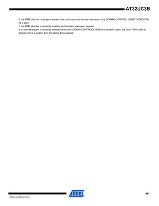
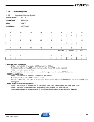


![450
32059L–AVR32–01/2012
AT32UC3B
22.8.3.8 Host Frame Number Register
Register Name: UHFNUM
Access Type: Read/Write
Offset: 0x0420
Reset Value: 0x00000000
• FLENHIGH: Frame Length
This field contains the 8 high-order bits of the 14-bits internal frame counter (frame counter at 12MHz, counter length is 12000
to ensure a SOF generation every 1 ms).
• FNUM: Frame Number
This field contains the current SOF number.
This field can be written.
31 30 29 28 27 26 25 24
- - - - - - - -
23 22 21 20 19 18 17 16
FLENHIGH
15 14 13 12 11 10 9 8
- - FNUM[10:5]
7 6 5 4 3 2 1 0
FNUM[4:0] - - -](https://image.slidesharecdn.com/doc32059-150506085255-conversion-gate02/85/Doc32059-450-320.jpg)
![454
32059L–AVR32–01/2012
AT32UC3B
22.8.3.12 Pipe n Configuration Register
Register Name: UPCFGn, n in [0..6]
Access Type: Read/Write
Offset: 0x0500 + (n * 0x04)
Reset Value: 0x00000000
• INTFRQ: Pipe Interrupt Request Frequency
This field contains the maximum value in millisecond of the polling period for an Interrupt Pipe.
This value has no effect for a non-Interrupt Pipe.
This field is cleared upon sending a USB reset.
• PEPNUM: Pipe Endpoint Number
This field contains the number of the endpoint targeted by the pipe. This value is from 0 to 15.
This field is cleared upon sending a USB reset.
• PTYPE: Pipe Type
This field contains the pipe type.
This field is cleared upon sending a USB reset.
• AUTOSW: Automatic Switch
This bit is cleared upon sending a USB reset.
1: The automatic bank switching is enabled.
0: The automatic bank switching is disabled.
31 30 29 28 27 26 25 24
INTFRQ
23 22 21 20 19 18 17 16
- - - - PEPNUM
15 14 13 12 11 10 9 8
- - PTYPE - AUTOSW PTOKEN
7 6 5 4 3 2 1 0
- PSIZE PBK ALLOC -
PTYPE Pipe Type
0 0 Control
0 1 Isochronous
1 0 Bulk
1 1 Interrupt](https://image.slidesharecdn.com/doc32059-150506085255-conversion-gate02/85/Doc32059-454-320.jpg)
![456
32059L–AVR32–01/2012
AT32UC3B
22.8.3.13 Pipe n Status Register
Register Name: UPSTAn, n in [0..6]
Access Type: Read-Only
Offset: 0x0530 + (n * 0x04)
Reset Value: 0x00000000
• PBYCT: Pipe Byte Count
This field contains the byte count of the FIFO.
For OUT pipe, incremented after each byte written by the user into the pipe and decremented after each byte sent to the
peripheral.
For IN pipe, incremented after each byte received from the peripheral and decremented after each byte read by the user from
the pipe.
This field may be updated 1 clock cycle after the RWALL bit changes, so the user should not poll this field as an interrupt bit.
• CFGOK: Configuration OK Status
This bit is set/cleared when the UPCFGn.ALLOC bit is set.
This bit is set if the pipe n number of banks (UPCFGn.PBK) and size (UPCFGn.PSIZE) are correct compared to the maximal
allowed number of banks and size for this pipe and to the maximal FIFO size (i.e., the DPRAM size).
If this bit is cleared, the user should rewrite correct values ot the PBK and PSIZE field in the UPCFGn register.
• RWALL: Read/Write Allowed
For OUT pipe, this bit is set when the current bank is not full, i.e., the software can write further data into the FIFO.
For IN pipe, this bit is set when the current bank is not empty, i.e., the software can read further data from the FIFO.
This bit is cleared otherwise.
This bit is also cleared when the RXSTALL or the PERR bit is one.
• CURRBK: Current Bank
For non-control pipe, this field indicates the number of the current bank.
31 30 29 28 27 26 25 24
- PBYCT[10:4]
23 22 21 20 19 18 17 16
PBYCT[3:0] - CFGOK - RWALL
15 14 13 12 11 10 9 8
CURRBK NBUSYBK - - DTSEQ
7 6 5 4 3 2 1 0
SHORT
PACKETI
RXSTALLDI/
CRCERRI
OVERFI NAKEDI PERRI
TXSTPI/
UNDERFI
TXOUTI RXINI
CURRBK Current Bank
0 0 Bank0](https://image.slidesharecdn.com/doc32059-150506085255-conversion-gate02/85/Doc32059-456-320.jpg)
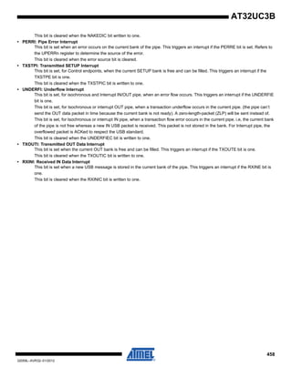
![459
32059L–AVR32–01/2012
AT32UC3B
22.8.3.14 Pipe n Status Clear Register
Register Name: UPSTAnCLR, n in [0..6]
Access Type: Write-Only
Offset: 0x0560 + (n * 0x04)
Read Value: 0x00000000
Writing a one to a bit in this register will clear the corresponding bit in UPSTAn.
Writing a zero to a bit in this register has no effect.
This bit always reads as zero.
31 30 29 28 27 26 25 24
- - - - - - - -
23 22 21 20 19 18 17 16
- - - - - - - -
15 14 13 12 11 10 9 8
- - - - - - - -
7 6 5 4 3 2 1 0
SHORT
PACKETIC
RXSTALLDI
C/
CRCERRIC
OVERFIC NAKEDIC -
TXSTPIC/
UNDERFIC
TXOUTIC RXINIC](https://image.slidesharecdn.com/doc32059-150506085255-conversion-gate02/85/Doc32059-459-320.jpg)
![460
32059L–AVR32–01/2012
AT32UC3B
22.8.3.15 Pipe n Status Set Register
Register Name: UPSTAnSET, n in [0..6]
Access Type: Write-Only
Offset: 0x0590 + (n * 0x04)
Read Value: 0x00000000
Writing a one to a bit in this register will set the corresponding bit in UPSTAn, what may be useful for test or debug purposes.
Writing a zero to a bit in this register has no effect.
This bit always reads as zero.
31 30 29 28 27 26 25 24
- - - - - - - -
23 22 21 20 19 18 17 16
- - - - - - - -
15 14 13 12 11 10 9 8
- - - NBUSYBKS - - - -
7 6 5 4 3 2 1 0
SHORT
PACKETIS
RXSTALLDIS/
CRCERRIS
OVERFIS NAKEDIS PERRIS
TXSTPIS/
UNDERFIS
TXOUTIS RXINIS](https://image.slidesharecdn.com/doc32059-150506085255-conversion-gate02/85/Doc32059-460-320.jpg)
![461
32059L–AVR32–01/2012
AT32UC3B
22.8.3.16 Pipe n Control Register
Register Name: UPCONn, n in [0..6]
Access Type: Read-Only
Offset: 0x05C0 + (n * 0x04)
Reset Value: 0x00000000
• RSTDT: Reset Data Toggle
This bit is set when the RSTDTS bit is written to one. This will reset the Data Toggle to its initial value for the current Pipe.
This bit is cleared when proceed.
• PFREEZE: Pipe Freeze
This bit is set when the PFREEZES bit is written to one or when the pipe is not configured or when a STALL handshake has
been received on this Pipe or when an error occurs on the Pipe (PERR is one) or when (INRQ+1) In requests have been
processed or when after a Pipe reset (UPRST.PRSTn rising) or a Pipe Enable (UPRST.PEN rising). This will Freeze the Pipe
requests generation.
This bit is cleared when the PFREEZEC bit is written to one. This will enable the Pipe request generation.
• PDISHDMA: Pipe Interrupts Disable HDMA Request Enable
See the UECONn.EPDISHDMA bit description.
• FIFOCON: FIFO Control
For OUT and SETUP Pipe:
This bit is set when the current bank is free, at the same time than TXOUTI or TXSTPI.
This bit is cleared when the FIFOCONC bit is written to one. This will send the FIFO data and switch the bank.
For IN Pipe:
This bit is set when a new IN message is stored in the current bank, at the same time than RXINI.
This bit is cleared when the FIFOCONC bit is written to one. This will free the current bank and switch to the next bank.
• NBUSYBKE: Number of Busy Banks Interrupt Enable
This bit is set when the NBUSYBKES bit is written to one.This will enable the Transmitted IN Data interrupt (NBUSYBKE).
This bit is cleared when the NBUSYBKEC bit is written to one. This will disable the Transmitted IN Data interrupt (NBUSYBKE).
• SHORTPACKETIE: Short Packet Interrupt Enable
This bit is set when the SHORTPACKETES bit is written to one. This will enable the Transmitted IN Data IT
(SHORTPACKETIE).
This bit is cleared when the SHORTPACKETEC bit is written to one. This will disable the Transmitted IN Data IT
(SHORTPACKETE).
31 30 29 28 27 26 25 24
- - - - - - - -
23 22 21 20 19 18 17 16
- - - - - RSTDT PFREEZE PDISHDMA
15 14 13 12 11 10 9 8
- FIFOCON - NBUSYBKE - - - -
7 6 5 4 3 2 1 0
SHORT
PACKETIE
RXSTALLDE
/CRCERRE
OVERFIE NAKEDE PERRE
TXSTPE/
UNDERFIE
TXOUTE RXINE](https://image.slidesharecdn.com/doc32059-150506085255-conversion-gate02/85/Doc32059-461-320.jpg)
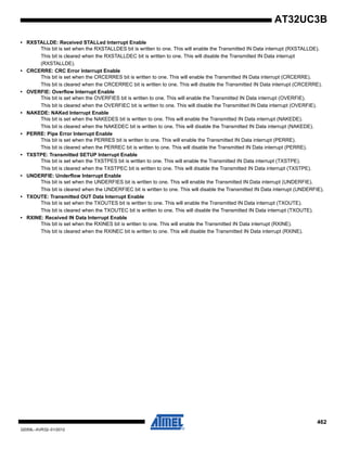
![463
32059L–AVR32–01/2012
AT32UC3B
22.8.3.17 Pipe n Control Clear Register
Register Name: UPCONnCLR, n in [0..6]
Access Type: Write-Only
Offset: 0x0620 + (n * 0x04)
Read Value: 0x00000000
Writing a one to a bit in this register will clear the corresponding bit in UPCONn.
Writing a zero to a bit in this register has no effect.
This bit always reads as zero.
31 30 29 28 27 26 25 24
- - - - - - - -
23 22 21 20 19 18 17 16
- - - - - - PFREEZEC PDISHDMAC
15 14 13 12 11 10 9 8
- FIFOCONC - NBUSYBKEC - - - -
7 6 5 4 3 2 1 0
SHORT
PACKETIEC
RXSTALLDEC
/CRCERREC
OVERFIEC NAKEDEC PERREC
TXSTPEC/
UNDERFIEC
TXOUTEC RXINEC](https://image.slidesharecdn.com/doc32059-150506085255-conversion-gate02/85/Doc32059-463-320.jpg)
![464
32059L–AVR32–01/2012
AT32UC3B
22.8.3.18 Pipe n Control Set Register
Register Name: UPCONnSET, n in [0..6]
Access Type: Write-Only
Offset: 0x05F0 + (n * 0x04)
Read Value: 0x00000000
Writing a one to a bit in this register will set the corresponding bit in UPCONn.
Writing a zero to a bit in this register has no effect.
This bit always reads as zero.
31 30 29 28 27 26 25 24
- - - - - - - -
23 22 21 20 19 18 17 16
- - - - - RSTDTS PFREEZES PDISHDMAS
15 14 13 12 11 10 9 8
- - - NBUSYBKES - - - -
7 6 5 4 3 2 1 0
SHORT
PACKETIES
RXSTALLDES/
CRCERRES
OVERFIES NAKEDES PERRES
TXSTPES/
UNDERFIES
TXOUTES RXINES](https://image.slidesharecdn.com/doc32059-150506085255-conversion-gate02/85/Doc32059-464-320.jpg)
![465
32059L–AVR32–01/2012
AT32UC3B
22.8.3.19 Pipe n IN Request Register
Register Name: UPINRQn, n in [0..6]
Access Type: Read/Write
Offset: 0x0650 + (n * 0x04)
Reset Value: 0x00000000
• INMODE: IN Request Mode
Writing a one to this bit will allow the USBB to perform infinite IN requests when the Pipe is not frozen.
Writing a zero to this bit will perform a pre-defined number of IN requests. This number is the INRQ field.
• INRQ: IN Request Number before Freeze
This field contains the number of IN transactions before the USBB freezes the pipe. The USBB will perform (INRQ+1) IN
requests before to freeze the Pipe. This counter is automatically decreased by 1 each time a IN request has been successfully
performed.
This register has no effect when the INMODE bit is one (infinite IN requests generation till the pipe is not frozen).
31 30 29 28 27 26 25 24
- - - - - - - -
23 22 21 20 19 18 17 16
- - - - - - - -
15 14 13 12 11 10 9 8
- - - - - - - INMODE
7 6 5 4 3 2 1 0
INRQ](https://image.slidesharecdn.com/doc32059-150506085255-conversion-gate02/85/Doc32059-465-320.jpg)
![466
32059L–AVR32–01/2012
AT32UC3B
22.8.3.20 Pipe n Error Register
Register Name: UPERRn, n in [0..6]
Access Type: Read/Write
Offset: 0x0680 + (n * 0x04)
Reset Value: 0x00000000
• COUNTER: Error Counter
This field is incremented each time an error occurs (CRC16, TIMEOUT, PID, DATAPID or DATATGL).
This field is cleared when receiving a good usb packet without any error.
When this field reaches 3 (i.e., 3 consecutive errors), this pipe is automatically frozen (UPCONn.PFREEZE is set).
Writing 0b00 to this field will clear the counter.
• CRC16: CRC16 Error
This bit is set when a CRC16 error has been detected.
Writing a zero to this bit will clear the bit.
Writing a one to this bit has no effect.
• TIMEOUT: Time-Out Error
This bit is set when a Time-Out error has been detected.
Writing a zero to this bit will clear the bit.
Writing a one to this bit has no effect.
• PID: PID Error
This bit is set when a PID error has been detected.
Writing a zero to this bit will clear the bit.
Writing a one to this bit has no effect.
• DATAPID: Data PID Error
This bit is set when a Data PID error has been detected.
Writing a zero to this bit will clear the bit.
Writing a one to this bit has no effect.
• DATATGL: Data Toggle Error
This bit is set when a Data Toggle error has been detected.
Writing a zero to this bit will clear the bit.
Writing a one to this bit has no effect.
31 30 29 28 27 26 25 24
- - - - - - - -
23 22 21 20 19 18 17 16
- - - - - - - -
15 14 13 12 11 10 9 8
- - - - - - - -
7 6 5 4 3 2 1 0
- COUNTER CRC16 TIMEOUT PID DATAPID DATATGL](https://image.slidesharecdn.com/doc32059-150506085255-conversion-gate02/85/Doc32059-466-320.jpg)
![467
32059L–AVR32–01/2012
AT32UC3B
22.8.3.21 Host DMA Channel n Next Descriptor Address Register
Register Name: UHDMAnNEXTDESC, n in [1..6]
Access Type: Read/Write
Offset: 0x0710 + (n - 1) * 0x10
Reset Value: 0x00000000
Same as Section 22.8.2.17.
31 30 29 28 27 26 25 24
NXTDESCADDR[31:24]
23 22 21 20 19 18 17 16
NXTDESCADDR[23:16]
15 14 13 12 11 10 9 8
NXTDESCADDR[15:8]
7 6 5 4 3 2 1 0
NXTDESCADDR[7:4] - - - -](https://image.slidesharecdn.com/doc32059-150506085255-conversion-gate02/85/Doc32059-467-320.jpg)
![468
32059L–AVR32–01/2012
AT32UC3B
22.8.3.22 Host DMA Channel n HSB Address Register
Register Name: UHDMAnADDR, n in [1..6]
Access Type: Read/Write
Offset: 0x0714 + (n - 1) * 0x10
Reset Value: 0x00000000
Same as Section 22.8.2.18.
31 30 29 28 27 26 25 24
HSBADDR[31:24]
23 22 21 20 19 18 17 16
HSBADDR[23:16]
15 14 13 12 11 10 9 8
HSBADDR[15:8]
7 6 5 4 3 2 1 0
HSBADDR[7:0]](https://image.slidesharecdn.com/doc32059-150506085255-conversion-gate02/85/Doc32059-468-320.jpg)
![469
32059L–AVR32–01/2012
AT32UC3B
22.8.3.23 USB Host DMA Channel n Control Register
Register Name: UHDMAnCONTROL, n in [1..6]
Access Type: Read/Write
Offset: 0x0718 + (n - 1) * 0x10
Reset Value: 0x00000000
Same as Section 22.8.2.19.
(just replace the IN endpoint term by OUT endpoint, and vice-versa)
31 30 29 28 27 26 25 24
CHBYTELENGTH[15:8]
23 22 21 20 19 18 17 16
CHBYTELENGTH[7:0]
15 14 13 12 11 10 9 8
- - - - - - - -
7 6 5 4 3 2 1 0
BURSTLOC
KEN
DESCLD
IRQEN
EOBUFF
IRQEN
EOTIRQEN DMAENDEN
BUFFCLOSE
INEN
LDNXTCHD
ESCEN
CHEN](https://image.slidesharecdn.com/doc32059-150506085255-conversion-gate02/85/Doc32059-469-320.jpg)
![470
32059L–AVR32–01/2012
AT32UC3B
22.8.3.24 USB Host DMA Channel n Status Register
Register Name: UHDMAnSTATUS, n in [1..6]
Access Type: Read/Write
Offset: 0x071C + (n - 1) * 0x10
Reset Value: 0x00000000
Same as Section 22.8.2.20.
31 30 29 28 27 26 25 24
CHBYTECNT[15:8]
23 22 21 20 19 18 17 16
CHBYTECNT[7:0]
15 14 13 12 11 10 9 8
- - - - - - - -
7 6 5 4 3 2 1 0
- DESCLD
STA
EOCHBUFFS
TA EOTSTA - - CHACTIVE CHEN](https://image.slidesharecdn.com/doc32059-150506085255-conversion-gate02/85/Doc32059-470-320.jpg)
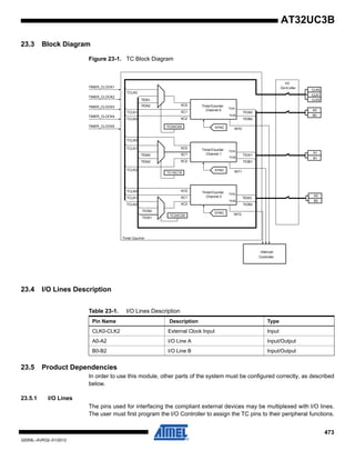
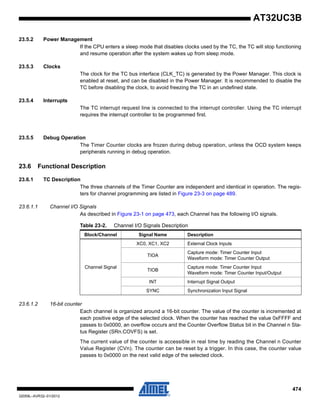
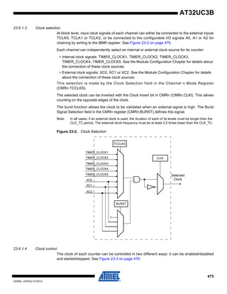
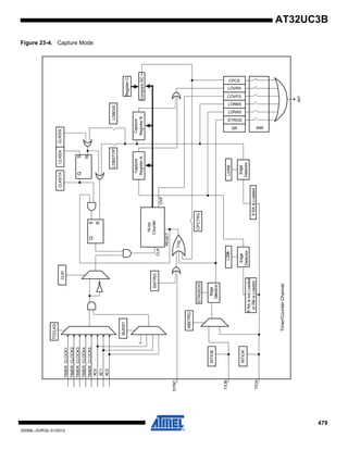
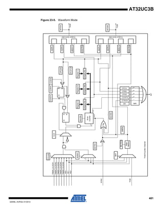
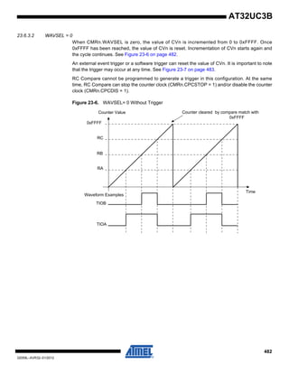
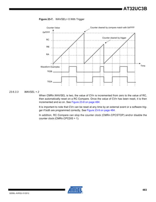
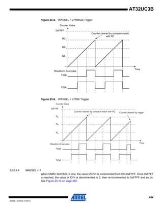
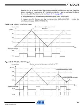
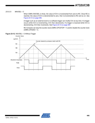
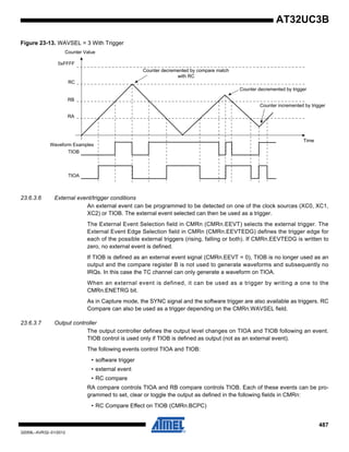

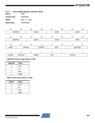
![498
32059L–AVR32–01/2012
AT32UC3B
23.7.4 Channel Counter Value Register
Name: CV
Access Type: Read-only
Offset: 0x10 + n * 0x40
Reset Value: 0x00000000
• CV: Counter Value
CV contains the counter value in real time.
31 30 29 28 27 26 25 24
- - - - - - - -
23 22 21 20 19 18 17 16
- - - - - - - -
15 14 13 12 11 10 9 8
CV[15:8]
7 6 5 4 3 2 1 0
CV[7:0]](https://image.slidesharecdn.com/doc32059-150506085255-conversion-gate02/85/Doc32059-498-320.jpg)
![499
32059L–AVR32–01/2012
AT32UC3B
23.7.5 Channel Register A
Name: RA
Access Type: Read-only if CMRn.WAVE = 0, Read/Write if CMRn.WAVE = 1
Offset: 0x14 + n * 0X40
Reset Value: 0x00000000
• RA: Register A
RA contains the Register A value in real time.
31 30 29 28 27 26 25 24
- - - - - - - -
23 22 21 20 19 18 17 16
- - - - - - - -
15 14 13 12 11 10 9 8
RA[15:8]
7 6 5 4 3 2 1 0
RA[7:0]](https://image.slidesharecdn.com/doc32059-150506085255-conversion-gate02/85/Doc32059-499-320.jpg)
![500
32059L–AVR32–01/2012
AT32UC3B
23.7.6 Channel Register B
Name: RB
Access Type: Read-only if CMRn.WAVE = 0, Read/Write if CMRn.WAVE = 1
Offset: 0x18 + n * 0x40
Reset Value: 0x00000000
• RB: Register B
RB contains the Register B value in real time.
31 30 29 28 27 26 25 24
- - - - - - - -
23 22 21 20 19 18 17 16
- - - - - - - -
15 14 13 12 11 10 9 8
RB[15:8]
7 6 5 4 3 2 1 0
RB[7:0]](https://image.slidesharecdn.com/doc32059-150506085255-conversion-gate02/85/Doc32059-500-320.jpg)
![501
32059L–AVR32–01/2012
AT32UC3B
23.7.7 Channel Register C
Name: RC
Access Type: Read/Write
Offset: 0x1C + n * 0x40
Reset Value: 0x00000000
• RC: Register C
RC contains the Register C value in real time.
31 30 29 28 27 26 25 24
- - - - - - - -
23 22 21 20 19 18 17 16
- - - - - - - -
15 14 13 12 11 10 9 8
RC[15:8]
7 6 5 4 3 2 1 0
RC[7:0]](https://image.slidesharecdn.com/doc32059-150506085255-conversion-gate02/85/Doc32059-501-320.jpg)
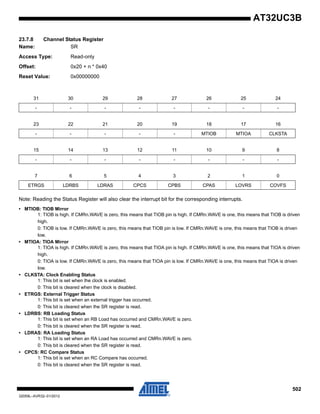
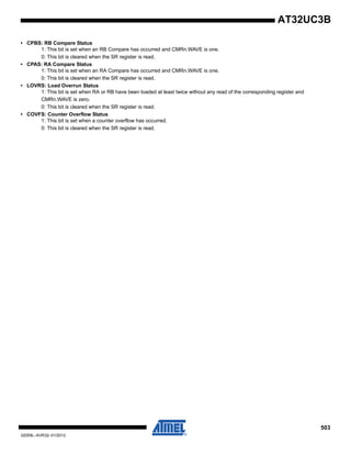


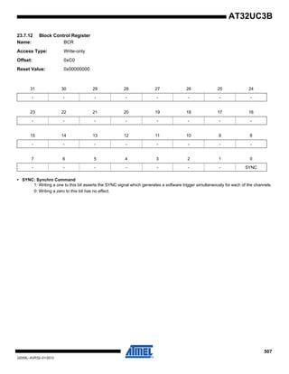
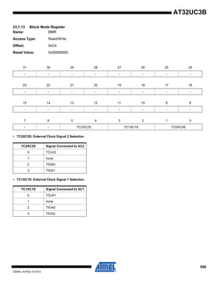
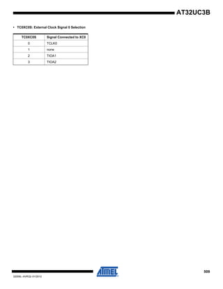

![511
32059L–AVR32–01/2012
AT32UC3B
23.7.15 Version Register
Name: VERSION
Access Type: Read-only
Offset: 0xFC
Reset Value: -
• VARIANT: Variant number
Reserved. No functionality associated.
• VERSION: Version number
Version number of the module. No functionality associated.
31 30 29 28 27 26 25 24
- - - - - - - -
23 22 21 20 19 18 17 16
- - - - VARIANT
15 14 13 12 11 10 9 8
- - - - VERSION[11:8]
7 6 5 4 3 2 1 0
VERSION[7:0]](https://image.slidesharecdn.com/doc32059-150506085255-conversion-gate02/85/Doc32059-511-320.jpg)
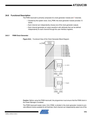
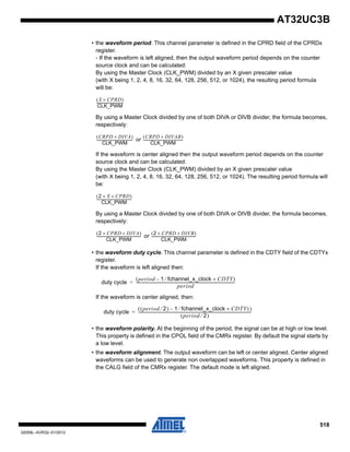
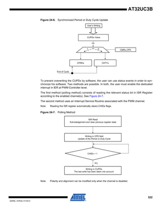
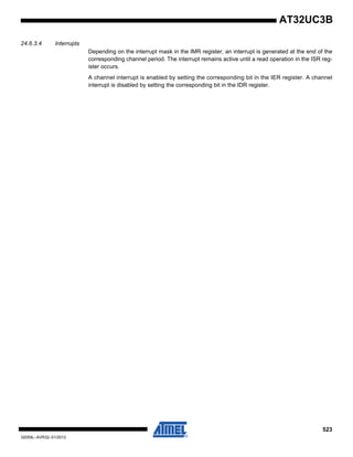
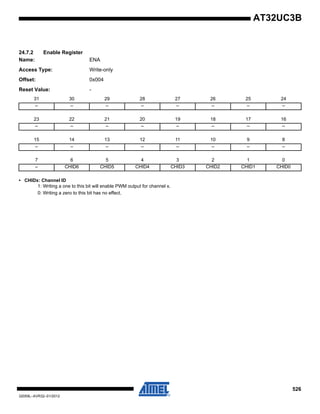
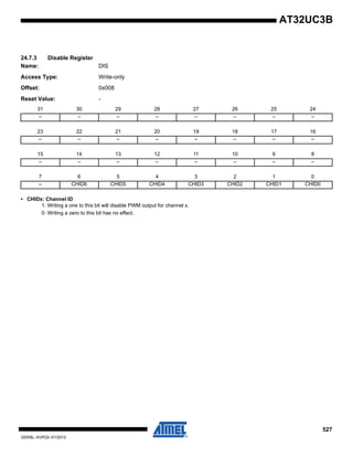
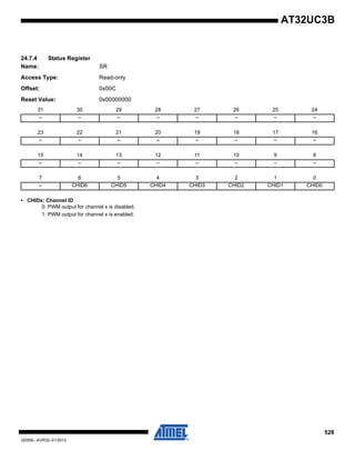
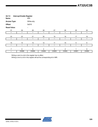

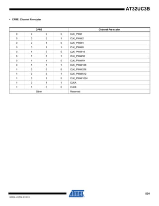
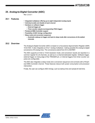
![540
32059L–AVR32–01/2012
AT32UC3B
25.3 Block Diagram
Figure 25-1. ADC Block Diagram
25.4 I/O Lines Description
25.5 Product Dependencies
In order to use this module, other parts of the system must be configured correctly, as described
below.
25.5.1 I/O Lines
The TRIGGER pin may be shared with other peripheral functions through the I/O Controller.
Table 25-1. ADC Pins Description
Pin Name Description
VDDANA Analog power supply
ADVREF Reference voltage
AD[0] - AD[7] Analog input channels
TRIGGER External trigger
Dedicated
Analog
Inputs
Analog Inputs
Multiplexed
With I/Olines
GND
AD-
AD-
AD-
AD-
AD-
AD-
ADVREF
VDDANA
TRIGGER
Trigger
Selection
ADC
Control
Logic
ADCInterrupt Interrupt
Controller
High Speed
Bus (HSB)
Peripheral
DMA
Controller
Peripheral Bridge
Peripheral Bus
(PB)
User
Interface
Successive
Approximation
Register
Analog-to-Digital
Converter
I/O
Controller
Timer
Counter
Channels](https://image.slidesharecdn.com/doc32059-150506085255-conversion-gate02/85/Doc32059-540-320.jpg)
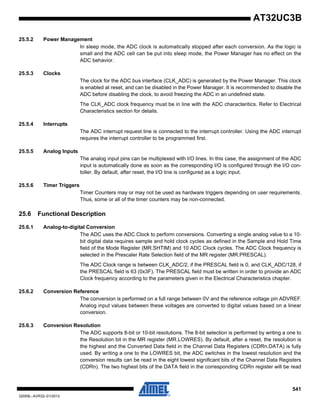
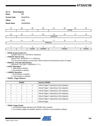
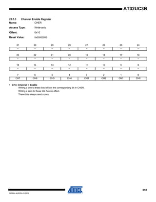
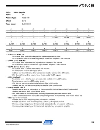
![553
32059L–AVR32–01/2012
AT32UC3B
25.7.7 Last Converted Data Register
Name: LCDR
Access Type: Read-only
Offset: 0x20
Reset Value: 0x00000000
• LDATA: Last Data Converted
The analog-to-digital conversion data is placed into this register at the end of a conversion and remains until a new conversion
is completed.
31 30 29 28 27 26 25 24
– – – – – – – –
23 22 21 20 19 18 17 16
– – – – – – – –
15 14 13 12 11 10 9 8
– – – – – – LDATA[9:8]
7 6 5 4 3 2 1 0
LDATA[7:0]](https://image.slidesharecdn.com/doc32059-150506085255-conversion-gate02/85/Doc32059-553-320.jpg)

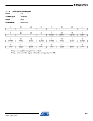
![557
32059L–AVR32–01/2012
AT32UC3B
25.7.11 Channel Data Register
Name: CDRx
Access Type: Read-only
Offset: 0x2C-0x4C
Reset Value: 0x00000000
• DATA: Converted Data
The analog-to-digital conversion data is placed into this register at the end of a conversion and remains until a new conversion
is completed. The Convert Data Register (CDR) is only loaded if the corresponding analog channel is enabled.
31 30 29 28 27 26 25 24
– – – – – – – –
23 22 21 20 19 18 17 16
– – – – – – – –
15 14 13 12 11 10 9 8
– – – – – – DATA[9:8]
7 6 5 4 3 2 1 0
DATA[7:0]](https://image.slidesharecdn.com/doc32059-150506085255-conversion-gate02/85/Doc32059-557-320.jpg)
![558
32059L–AVR32–01/2012
AT32UC3B
25.7.12 Version Register
Name: VERSION
Access Type: Read-only
Offset: 0xFC
Reset Value: –
• VARIANT: Variant Number
Reserved. No functionality associated.
• VERSION: Version Number
Version number of the module. No functionality associated.
31 30 29 28 27 26 25 24
– – – – – – – –
23 22 21 20 19 18 17 16
– – – – VARIANT
15 14 13 12 11 10 9 8
– – – – VERSION[11:8]
7 6 5 4 3 2 1 0
VERSION[7:0]](https://image.slidesharecdn.com/doc32059-150506085255-conversion-gate02/85/Doc32059-558-320.jpg)
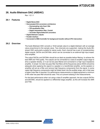
![561
32059L–AVR32–01/2012
AT32UC3B
26.3 Block Diagram
Figure 26-1. ABDAC Block Diagram
26.4 I/O Lines Description
26.5 Product Dependencies
In order to use this module, other parts of the system must be configured correctly, as described
below.
26.5.1 I/O Lines
The output pins used for the output bitstream from the Audio Bitstream DAC may be multiplexed
with IO lines.
Before using the Audio Bitstream DAC, the I/O Controller must be configured in order for the
Audio Bitstream DAC I/O lines to be in Audio Bitstream DAC peripheral mode.
Table 26-1. I/O Lines Description
Pin Name Pin Description Type
DATA0 Output from Audio Bitstream DAC Channel 0 Output
DATA1 Output from Audio Bitstream DAC Channel 1 Output
DATAN0 Inverted output from Audio Bitstream DAC Channel 0 Output
DATAN1 Inverted output from Audio Bitstream DAC Channel 1 Output
Clock Generator
Equalization FIR
COMB
(INT=128)
Sigma-Delta
DA-MOD
Equalization FIR
COMB
(INT=128)
Sigma-Delta
DA-MOD
bit_clk
DATA0
DATA1
GCLK_ABDAC
sample_clk
CHANNEL0[15:0]
Audio BitstreamDAC
PM
User Interface
CHANNEL1[15:0]](https://image.slidesharecdn.com/doc32059-150506085255-conversion-gate02/85/Doc32059-561-320.jpg)
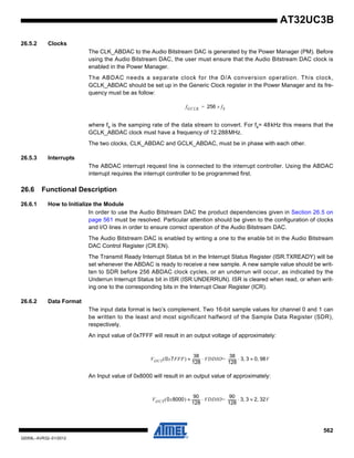
![564
32059L–AVR32–01/2012
AT32UC3B
26.6.9 Frequency Response
Figure 26-2. Frequency Response, EQ-FIR+COMB4
0 1 2 3 4 5 6 7 8 9 1 0
x 1 0
4
- 6 0
- 5 0
- 4 0
- 3 0
- 2 0
- 1 0
0
1 0
F r e q u e n c y [ F s ]
Amplitude[dB]](https://image.slidesharecdn.com/doc32059-150506085255-conversion-gate02/85/Doc32059-564-320.jpg)
![566
32059L–AVR32–01/2012
AT32UC3B
26.7.1 Sample Data Register
Name: SDR
Access Type: Read/Write
Offset: 0x00
Reset Value: 0x00000000
• CHANNEL1: Sample Data for Channel 1
signed 16-bit Sample Data for channel 1.
• CHANNEL0: Signed 16-bit Sample Data for Channel 0
signed 16-bit Sample Data for channel 0.
31 30 29 28 27 26 25 24
CHANNEL1[15:8]
23 22 21 20 19 18 17 16
CHANNEL1[7:0]
15 14 13 12 11 10 9 8
CHANNEL0[15:8]
7 6 5 4 3 2 1 0
CHANNEL0[7:0]](https://image.slidesharecdn.com/doc32059-150506085255-conversion-gate02/85/Doc32059-566-320.jpg)

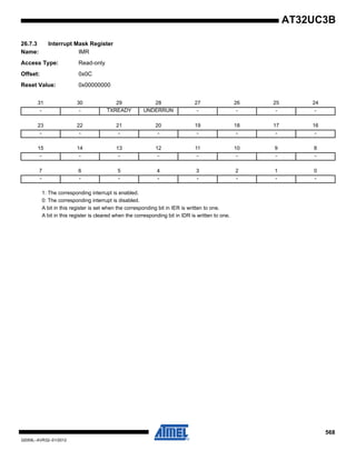

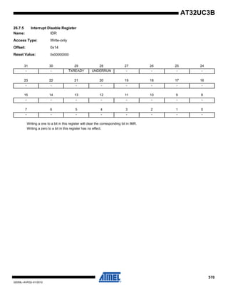

![573
32059L–AVR32–01/2012
AT32UC3B
27. Programming and Debugging
27.1 Overview
General description of programming and debug features, block diagram and introduction of main
concepts.
27.2 Service Access Bus
The AVR32 architecture offers a common interface for access to On-Chip Debug, programming,
and test functions. These are mapped on a common bus called the Service Access Bus (SAB),
which is linked to the JTAG port through a bus master module, which also handles synchroniza-
tion between the debugger and SAB clocks.
When accessing the SAB through the debugger there are no limitations on debugger frequency
compared to chip frequency, although there must be an active system clock in order for the SAB
accesses to complete. If the system clock is switched off in sleep mode, activity on the debugger
will restart the system clock automatically, without waking the device from sleep. Debuggers
may optimize the transfer rate by adjusting the frequency in relation to the system clock. This
ratio can be measured with debug protocol specific instructions.
The Service Access Bus uses 36 address bits to address memory or registers in any of the
slaves on the bus. The bus supports sized accesses of bytes (8 bits), halfwords (16 bits), or
words (32 bits). All accesses must be aligned to the size of the access, i.e. halfword accesses
must have the lowest address bit cleared, and word accesses must have the two lowest address
bits cleared.
27.2.1 SAB address map
The Service Access Bus (SAB) gives the user access to the internal address space and other
features through a 36 bits address space. The 4 MSBs identify the slave number, while the 32
LSBs are decoded within the slave’s address space. The SAB slaves are shown in Table 27-1
on page 573.
27.2.2 SAB security restrictions
The Service Access bus can be restricted by internal security measures. A short description of
the security measures are found in the table below.
Table 27-1. SAB Slaves, addresses and descriptions.
Slave Address [35:32] Description
Unallocated 0x0 Intentionally unallocated
OCD 0x1 OCD registers
HSB 0x4 HSB memory space, as seen by the CPU
HSB 0x5
Alternative mapping for HSB space, for compatibility with
other 32-bit AVR devices.
Memory Service
Unit
0x6 Memory Service Unit registers
Reserved Other Unused](https://image.slidesharecdn.com/doc32059-150506085255-conversion-gate02/85/Doc32059-573-320.jpg)
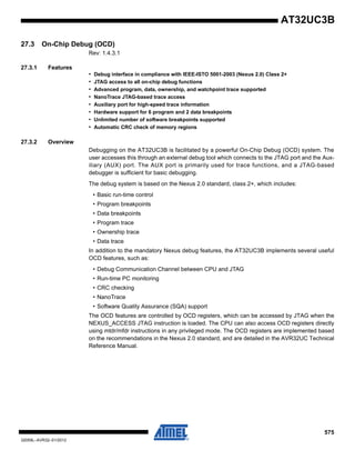
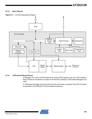
![579
32059L–AVR32–01/2012
AT32UC3B
Debug tools utilizing the AUX port should connect to the device through a Nexus-compliant Mic-
tor-38 connector, as described in the AVR32UC Technical Reference manual. This connector
includes the JTAG signals and the RESET_N pin, giving full access to the programming and
debug features in the device.
Figure 27-3. AUX+JTAG based Debugger
27.3.6.1 trace operation
Trace features are enabled by writing OCD registers by JTAG. The OCD extracts the trace infor-
mation from the CPU, compresses this information and formats it into variable-length messages
according to the Nexus standard. The messages are buffered in a 16-frame transmit queue, and
are output on the AUX port one frame at a time.
Table 27-5. Auxiliary Port Signals
Signal Direction Description
MCKO Output Trace data output clock
MDO[5:0] Output Trace data output
MSEO[1:0] Output Trace frame control
EVTI_N Input Event In
EVTO_N Output Event Out
A V R 3 2
A U X + J T A G
d e b u g to o l
J T A G
A U X
h ig h s p e e d
M ic to r 3 8
T r a c e b u ffe r
P C](https://image.slidesharecdn.com/doc32059-150506085255-conversion-gate02/85/Doc32059-579-320.jpg)
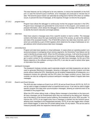
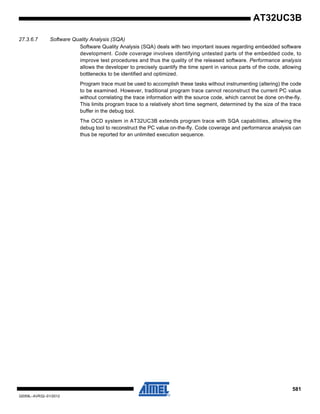
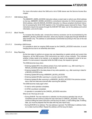
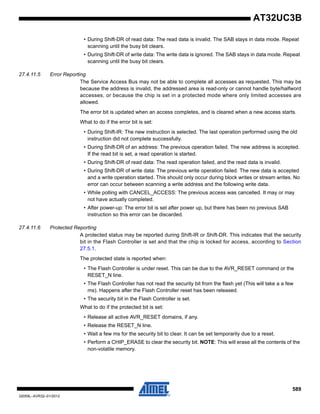
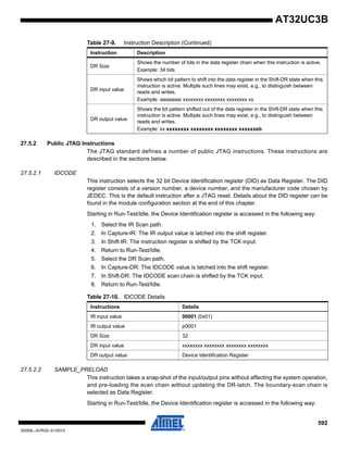
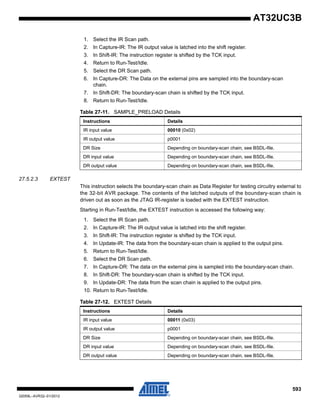
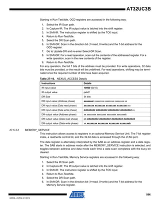
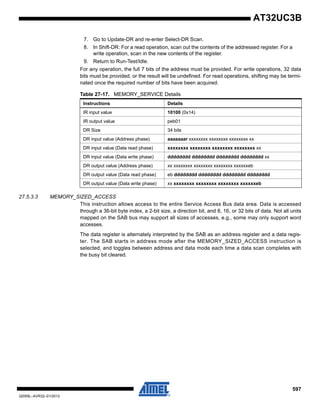
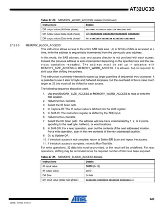
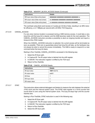
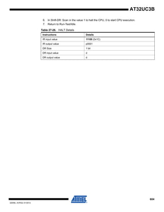
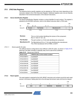
![606
32059L–AVR32–01/2012
AT32UC3B
Note: This register is primarily intended for compatibility with other 32-bit AVR devices. Certain
operations may not function correctly when parts of the system are reset. It is generally recom-
mended to only write 0x11111 or 0x00000 to these bits to ensure no unintended side effects
occur.
27.6.3 Boundary-Scan Chain
The Boundary-Scan Chain has the capability of driving and observing the logic levels on the dig-
ital I/O pins, as well as driving and observing the logic levels between the digital I/O pins and the
internal logic. Typically, output value, output enable, and input data are all available in the
boundary scan chain.
The boundary scan chain is described in the BDSL (Boundary Scan Description Language) file
available at the Atmel web site.
27.7 SAB address map
The Service Access Bus (SAB) gives the user access to the internal address space and other
features through a 36 bits address space. The 4 MSBs identify the slave number, while the 32
LSBs are decoded within the slave’s address space. The SAB slaves are shown in Table 27-28.
CPU CPU
APP HSB and PB buses
OCD On-Chip Debug logic and registers
RSERVED No effect
Table 27-28. SAB Slaves, addresses and descriptions.
Slave Address [35:32] Description
Unallocated 0x0 Intentionally unallocated
OCD 0x1 OCD registers
HSB 0x4 HSB memory space, as seen by the CPU
HSB 0x5
Alternative mapping for HSB space, for compatibility with
other 32-bit AVR devices.
Memory Service
Unit
0x6 Memory Service Unit registers
Reserved Other Unused](https://image.slidesharecdn.com/doc32059-150506085255-conversion-gate02/85/Doc32059-606-320.jpg)
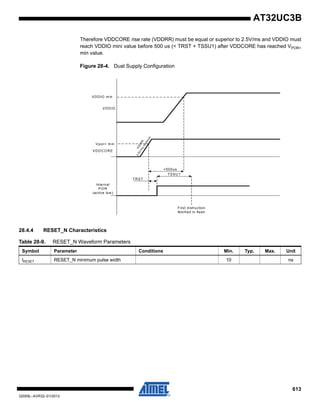
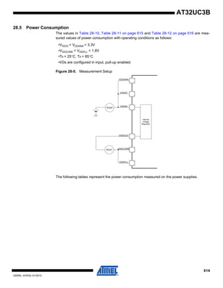
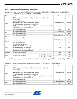
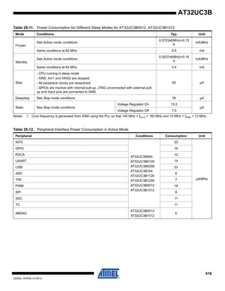
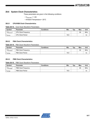
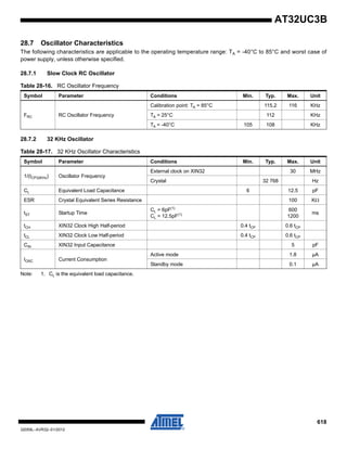
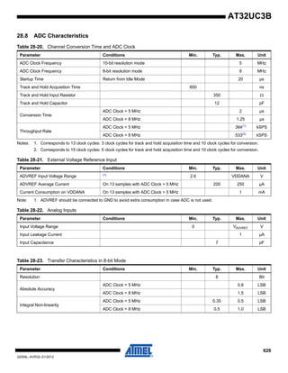
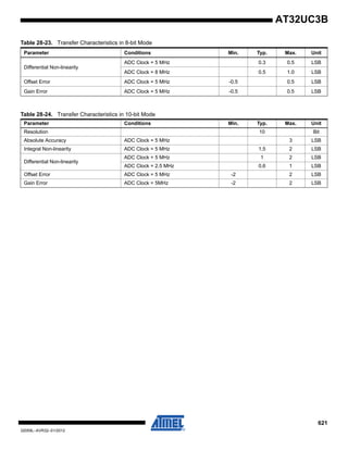
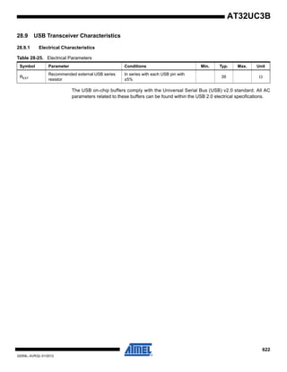
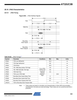
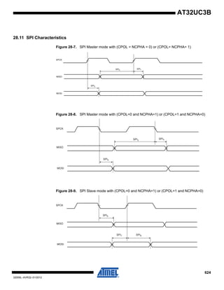
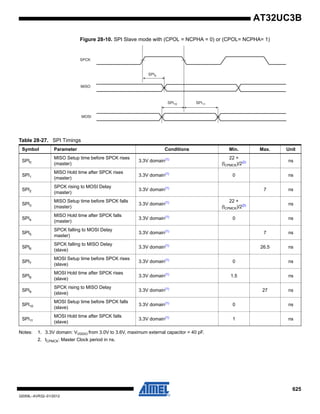
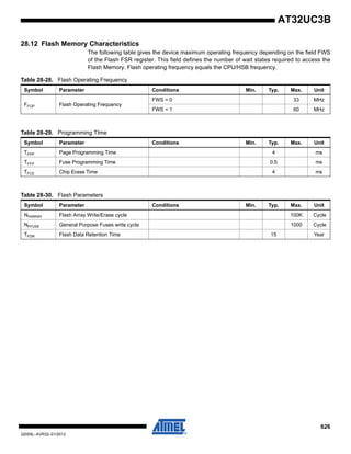
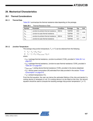
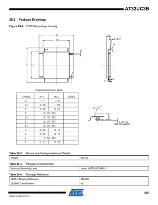
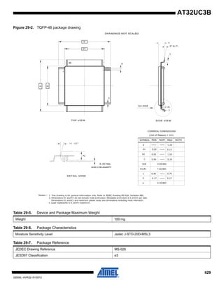
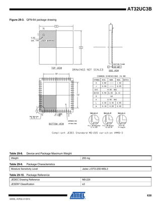
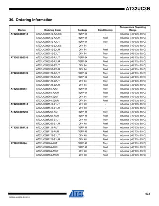
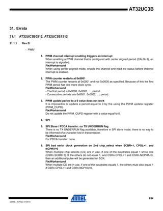
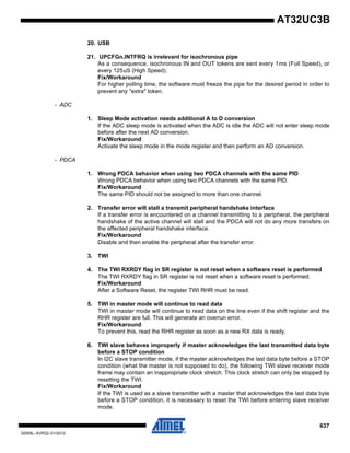
![638
32059L–AVR32–01/2012
AT32UC3B
7. TC
8. Channel chaining skips first pulse for upper channel
When chaining two channels using the Block Mode Register, the first pulse of the clock
between the channels is skipped.
Fix/Workaround
Configure the lower channel with RA = 0x1 and RC = 0x2 to produce a dummy clock cycle
for the upper channel. After the dummy cycle has been generated, indicated by the
SR.CPCS bit, reconfigure the RA and RC registers for the lower channel with the real
values.
- Processor and Architecture
1. LDM instruction with PC in the register list and without ++ increments Rp
For LDM with PC in the register list: the instruction behaves as if the ++ field is always set, ie
the pointer is always updated. This happens even if the ++ field is cleared. Specifically, the
increment of the pointer is done in parallel with the testing of R12.
Fix/Workaround
None.
2. RETE instruction does not clear SREG[L] from interrupts
The RETE instruction clears SREG[L] as expected from exceptions.
Fix/Workaround
When using the STCOND instruction, clear SREG[L] in the stacked value of SR before
returning from interrupts with RETE.
3. Privilege violation when using interrupts in application mode with protected system
stack
If the system stack is protected by the MPU and an interrupt occurs in application mode, an
MPU DTLB exception will occur.
Fix/Workaround
Make a DTLB Protection (Write) exception handler which permits the interrupt request to be
handled in privileged mode.
4. USART
5. ISO7816 info register US_NER cannot be read
The NER register always returns zero.
Fix/Workaround
None.
6. ISO7816 Mode T1: RX impossible after any TX
RX impossible after any TX.
Fix/Workaround
SOFT_RESET on RX+ Config US_MR + Config_US_CR.
7. The RTS output does not function correctly in hardware handshaking mode
The RTS signal is not generated properly when the USART receives data in hardware hand-
shaking mode. When the Peripheral DMA receive buffer becomes full, the RTS output
should go high, but it will stay low.
Fix/Workaround
Do not use the hardware handshaking mode of the USART. If it is necessary to drive the
RTS output high when the Peripheral DMA receive buffer becomes full, use the normal
mode of the USART. Configure the Peripheral DMA Controller to signal an interrupt when](https://image.slidesharecdn.com/doc32059-150506085255-conversion-gate02/85/Doc32059-638-320.jpg)
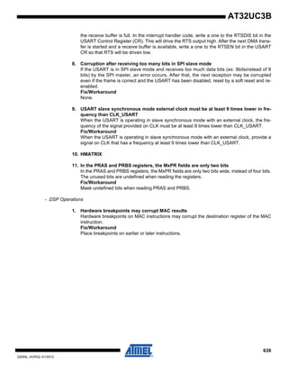
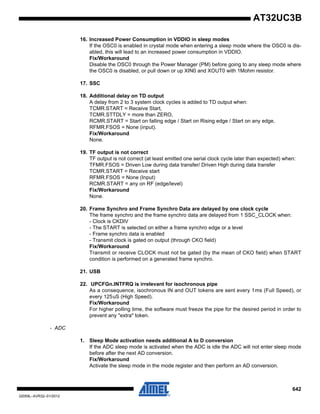
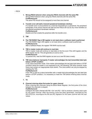
![644
32059L–AVR32–01/2012
AT32UC3B
- Processor and Architecture
1. LDM instruction with PC in the register list and without ++ increments Rp
For LDM with PC in the register list: the instruction behaves as if the ++ field is always set, ie
the pointer is always updated. This happens even if the ++ field is cleared. Specifically, the
increment of the pointer is done in parallel with the testing of R12.
Fix/Workaround
None.
2. RETE instruction does not clear SREG[L] from interrupts
The RETE instruction clears SREG[L] as expected from exceptions.
Fix/Workaround
When using the STCOND instruction, clear SREG[L] in the stacked value of SR before
returning from interrupts with RETE.
3. Privilege violation when using interrupts in application mode with protected system
stack
If the system stack is protected by the MPU and an interrupt occurs in application mode, an
MPU DTLB exception will occur.
Fix/Workaround
Make a DTLB Protection (Write) exception handler which permits the interrupt request to be
handled in privileged mode.
4. Flash
5. Reset vector is 80000020h rather than 80000000h
Reset vector is 80000020h rather than 80000000h.
Fix/Workaround
The flash program code must start at the address 80000020h. The flash memory range
80000000h-80000020h must be programmed with 00000000h.
- USART
1. ISO7816 info register US_NER cannot be read
The NER register always returns zero.
Fix/Workaround
None.
2. ISO7816 Mode T1: RX impossible after any TX
RX impossible after any TX.
Fix/Workaround
SOFT_RESET on RX+ Config US_MR + Config_US_CR.
3. The RTS output does not function correctly in hardware handshaking mode
The RTS signal is not generated properly when the USART receives data in hardware hand-
shaking mode. When the Peripheral DMA receive buffer becomes full, the RTS output
should go high, but it will stay low.
Fix/Workaround
Do not use the hardware handshaking mode of the USART. If it is necessary to drive the
RTS output high when the Peripheral DMA receive buffer becomes full, use the normal
mode of the USART. Configure the Peripheral DMA Controller to signal an interrupt when
the receive buffer is full. In the interrupt handler code, write a one to the RTSDIS bit in the
USART Control Register (CR). This will drive the RTS output high. After the next DMA trans-](https://image.slidesharecdn.com/doc32059-150506085255-conversion-gate02/85/Doc32059-644-320.jpg)
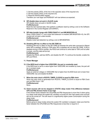

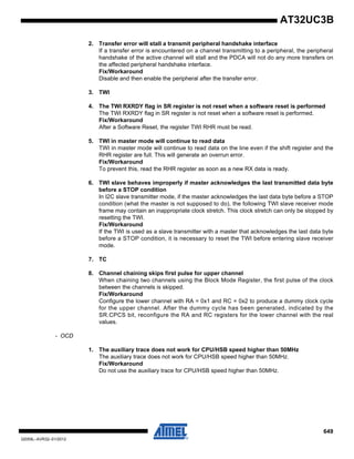
![650
32059L–AVR32–01/2012
AT32UC3B
- Processor and Architecture
1. LDM instruction with PC in the register list and without ++ increments Rp
For LDM with PC in the register list: the instruction behaves as if the ++ field is always set, ie
the pointer is always updated. This happens even if the ++ field is cleared. Specifically, the
increment of the pointer is done in parallel with the testing of R12.
Fix/Workaround
None.
2. RETE instruction does not clear SREG[L] from interrupts
The RETE instruction clears SREG[L] as expected from exceptions.
Fix/Workaround
When using the STCOND instruction, clear SREG[L] in the stacked value of SR before
returning from interrupts with RETE.
3. Privilege violation when using interrupts in application mode with protected system
stack
If the system stack is protected by the MPU and an interrupt occurs in application mode, an
MPU DTLB exception will occur.
Fix/Workaround
Make a DTLB Protection (Write) exception handler which permits the interrupt request to be
handled in privileged mode.
4. USART
5. ISO7816 info register US_NER cannot be read
The NER register always returns zero.
Fix/Workaround
None.
6. ISO7816 Mode T1: RX impossible after any TX
RX impossible after any TX.
Fix/Workaround
SOFT_RESET on RX+ Config US_MR + Config_US_CR.
7. The RTS output does not function correctly in hardware handshaking mode
The RTS signal is not generated properly when the USART receives data in hardware hand-
shaking mode. When the Peripheral DMA receive buffer becomes full, the RTS output
should go high, but it will stay low.
Fix/Workaround
Do not use the hardware handshaking mode of the USART. If it is necessary to drive the
RTS output high when the Peripheral DMA receive buffer becomes full, use the normal
mode of the USART. Configure the Peripheral DMA Controller to signal an interrupt when
the receive buffer is full. In the interrupt handler code, write a one to the RTSDIS bit in the
USART Control Register (CR). This will drive the RTS output high. After the next DMA trans-
fer is started and a receive buffer is available, write a one to the RTSEN bit in the USART
CR so that RTS will be driven low.
8. Corruption after receiving too many bits in SPI slave mode
If the USART is in SPI slave mode and receives too much data bits (ex: 9bitsinstead of 8
bits) by the SPI master, an error occurs. After that, the next reception may be corrupted](https://image.slidesharecdn.com/doc32059-150506085255-conversion-gate02/85/Doc32059-650-320.jpg)


![656
32059L–AVR32–01/2012
AT32UC3B
- OCD
1. The auxiliary trace does not work for CPU/HSB speed higher than 50MHz
The auxiliary trace does not work for CPU/HSB speed higher than 50MHz.
Fix/Workaround
Do not use the auxiliary trace for CPU/HSB speed higher than 50MHz.
- Processor and Architecture
1. LDM instruction with PC in the register list and without ++ increments Rp
For LDM with PC in the register list: the instruction behaves as if the ++ field is always set, ie
the pointer is always updated. This happens even if the ++ field is cleared. Specifically, the
increment of the pointer is done in parallel with the testing of R12.
Fix/Workaround
None.
2. RETE instruction does not clear SREG[L] from interrupts
The RETE instruction clears SREG[L] as expected from exceptions.
Fix/Workaround
When using the STCOND instruction, clear SREG[L] in the stacked value of SR before
returning from interrupts with RETE.
3. RETS behaves incorrectly when MPU is enabled
RETS behaves incorrectly when MPU is enabled and MPU is configured so that system
stack is not readable in unprivileged mode.
Fix/Workaround
Make system stack readable in unprivileged mode, or return from supervisor mode using
rete instead of rets. This requires:
1. Changing the mode bits from 001 to 110 before issuing the instruction. Updating the
mode bits to the desired value must be done using a single mtsr instruction so it is done
atomically. Even if this step is generally described as not safe in the UC technical reference
manual, it is safe in this very specific case.
2. Execute the RETE instruction.
4. Privilege violation when using interrupts in application mode with protected system
stack
If the system stack is protected by the MPU and an interrupt occurs in application mode, an
MPU DTLB exception will occur.
Fix/Workaround
Make a DTLB Protection (Write) exception handler which permits the interrupt request to be
handled in privileged mode.
5. USART
6. ISO7816 info register US_NER cannot be read
The NER register always returns zero.
Fix/Workaround
None.
7. ISO7816 Mode T1: RX impossible after any TX
RX impossible after any TX.
Fix/Workaround
SOFT_RESET on RX+ Config US_MR + Config_US_CR.](https://image.slidesharecdn.com/doc32059-150506085255-conversion-gate02/85/Doc32059-656-320.jpg)


![663
32059L–AVR32–01/2012
AT32UC3B
SR.CPCS bit, reconfigure the RA and RC registers for the lower channel with the real
values.
- OCD
1. The auxiliary trace does not work for CPU/HSB speed higher than 50MHz
The auxiliary trace does not work for CPU/HSB speed higher than 50MHz.
Fix/Workaround
Do not use the auxiliary trace for CPU/HSB speed higher than 50MHz.
- Processor and Architecture
1. LDM instruction with PC in the register list and without ++ increments Rp
For LDM with PC in the register list: the instruction behaves as if the ++ field is always set, ie
the pointer is always updated. This happens even if the ++ field is cleared. Specifically, the
increment of the pointer is done in parallel with the testing of R12.
Fix/Workaround
None.
2. RETE instruction does not clear SREG[L] from interrupts
The RETE instruction clears SREG[L] as expected from exceptions.
Fix/Workaround
When using the STCOND instruction, clear SREG[L] in the stacked value of SR before
returning from interrupts with RETE.
3. RETS behaves incorrectly when MPU is enabled
RETS behaves incorrectly when MPU is enabled and MPU is configured so that system
stack is not readable in unprivileged mode.
Fix/Workaround
Make system stack readable in unprivileged mode, or return from supervisor mode using
rete instead of rets. This requires:
1. Changing the mode bits from 001 to 110 before issuing the instruction. Updating the
mode bits to the desired value must be done using a single mtsr instruction so it is done
atomically. Even if this step is generally described as not safe in the UC technical reference
manual, it is safe in this very specific case.
2. Execute the RETE instruction.
4. Privilege violation when using interrupts in application mode with protected system
stack
If the system stack is protected by the MPU and an interrupt occurs in application mode, an
MPU DTLB exception will occur.
Fix/Workaround
Make a DTLB Protection (Write) exception handler which permits the interrupt request to be
handled in privileged mode.
5. USART
6. ISO7816 info register US_NER cannot be read
The NER register always returns zero.
Fix/Workaround
None.](https://image.slidesharecdn.com/doc32059-150506085255-conversion-gate02/85/Doc32059-663-320.jpg)
![666
32059L–AVR32–01/2012
AT32UC3B
31.2.4 Rev. B
- PWM
1. PWM channel interrupt enabling triggers an interrupt
When enabling a PWM channel that is configured with center aligned period (CALG=1), an
interrupt is signalled.
Fix/Workaround
When using center aligned mode, enable the channel and read the status before channel
interrupt is enabled.
2. PWN counter restarts at 0x0001
The PWM counter restarts at 0x0001 and not 0x0000 as specified. Because of this the first
PWM period has one more clock cycle.
Fix/Workaround
- The first period is 0x0000, 0x0001, ..., period.
- Consecutive periods are 0x0001, 0x0002, ..., period.
3. PWM update period to a 0 value does not work
It is impossible to update a period equal to 0 by the using the PWM update register
(PWM_CUPD).
Fix/Workaround
Do not update the PWM_CUPD register with a value equal to 0.
4. PWM channel status may be wrong if disabled before a period has elapsed
Before a PWM period has elapsed, the read channel status may be wrong. The CHIDx-bit
for a PWM channel in the PWM Enable Register will read '1' for one full PWM period even if
the channel was disabled before the period elapsed. It will then read '0' as expected.
Fix/Workaround
Reading the PWM channel status of a disabled channel is only correct after a PWM period
has elapsed.
5. The following alternate C functions PWM[4] on PA16 and PWM[6] on PA31 are not
available on Rev B
The following alternate C functions PWM[4] on PA16 and PWM[6] on PA31 are not available
on Rev B.
Fix/Workaround
Do not use these PWM alternate functions on these pins.
6. SPI
7. SPI Slave / PDCA transfer: no TX UNDERRUN flag
There is no TX UNDERRUN flag available, therefore in SPI slave mode, there is no way to
be informed of a character lost in transmission.
Fix/Workaround
For PDCA transfer: none.](https://image.slidesharecdn.com/doc32059-150506085255-conversion-gate02/85/Doc32059-666-320.jpg)
![668
32059L–AVR32–01/2012
AT32UC3B
- SSC
1. SSC does not trigger RF when data is low
The SSC cannot transmit or receive data when CKS = CKDIV and CKO = none, in TCMR or
RCMR respectively.
Fix/Workaround
Set CKO to a value that is not "none" and bypass the output of the TK/RK pin with the GPIO.
- USB
1. USB No end of host reset signaled upon disconnection
In host mode, in case of an unexpected device disconnection whereas a usb reset is being
sent by the usb controller, the UHCON.RESET bit may not been cleared by the hardware at
the end of the reset.
Fix/Workaround
A software workaround consists in testing (by polling or interrupt) the disconnection
(UHINT.DDISCI == 1) while waiting for the end of reset (UHCON.RESET == 0) to avoid
being stuck.
2. USBFSM and UHADDR1/2/3 registers are not available
Do not use USBFSM register.
Fix/Workaround
Do not use USBFSM register and use HCON[6:0] field instead for all the pipes.
- Cycle counter
1. CPU Cycle Counter does not reset the COUNT system register on COMPARE match.
The device revision B does not reset the COUNT system register on COMPARE match. In
this revision, the COUNT register is clocked by the CPU clock, so when the CPU clock
stops, so does incrementing of COUNT.
Fix/Workaround
None.
- ADC
1. ADC possible miss on DRDY when disabling a channel
The ADC does not work properly when more than one channel is enabled.
Fix/Workaround
Do not use the ADC with more than one channel enabled at a time.
2. ADC OVRE flag sometimes not reset on Status Register read
The OVRE flag does not clear properly if read simultaneously to an end of conversion.
Fix/Workaround
None.
3. Sleep Mode activation needs additional A to D conversion
If the ADC sleep mode is activated when the ADC is idle the ADC will not enter sleep mode
before after the next AD conversion.
Fix/Workaround
Activate the sleep mode in the mode register and then perform an AD conversion.](https://image.slidesharecdn.com/doc32059-150506085255-conversion-gate02/85/Doc32059-668-320.jpg)
![670
32059L–AVR32–01/2012
AT32UC3B
2. The command Quick Page Read User Page(QPRUP) is not functional
The command Quick Page Read User Page(QPRUP) is not functional.
Fix/Workaround
None.
3. PAGEN Semantic Field for Program GP Fuse Byte is WriteData[7:0], ByteAddress[1:0]
on revision B instead of WriteData[7:0], ByteAddress[2:0]
PAGEN Semantic Field for Program GP Fuse Byte is WriteData[7:0], ByteAddress[1:0] on
revision B instead of WriteData[7:0], ByteAddress[2:0].
Fix/Workaround
None.
4. Reading from on-chip flash may fail after a flash fuse write operation (FLASHC LP,
UP, WGPB, EGPB, SSB, PGPFB, EAGPF commands).
After a flash fuse write operation (FLASHC LP, UP, WGPB, EGPB, SSB, PGPFB, EAGPF
commands), the following flash read access may return corrupted data. This erratum does
not affect write operations to regular flash memory.
Fix/Workaround
The flash fuse write operation (FLASHC LP, UP, WGPB, EGPB, SSB, PGPFB, EAGPF
commands) must be issued from internal RAM. After the write operation, perform a dummy
flash page write operation (FLASHC WP). Content and location of this page is not important
and filling the write buffer with all one (FFh) will leave the current flash content unchanged. It
is then safe to read and fetch code from the flash.
5.
- RTC
1. Writes to control (CTRL), top (TOP) and value (VAL) in the RTC are discarded if the
RTC peripheral bus clock (PBA) is divided by a factor of four or more relative to the
HSB clock
Writes to control (CTRL), top (TOP) and value (VAL) in the RTC are discarded if the RTC
peripheral bus clock (PBA) is divided by a factor of four or more relative to the HSB clock.
Fix/Workaround
Do not write to the RTC registers using the peripheral bus clock (PBA) divided by a factor of
four or more relative to the HSB clock.
2. The RTC CLKEN bit (bit number 16) of CTRL register is not available
The RTC CLKEN bit (bit number 16) of CTRL register is not available.
Fix/Workaround
Do not use the CLKEN bit of the RTC on Rev B.](https://image.slidesharecdn.com/doc32059-150506085255-conversion-gate02/85/Doc32059-670-320.jpg)
![672
32059L–AVR32–01/2012
AT32UC3B
Figure 31-1. Timer/Counter clock connections on RevB
7. Spurious interrupt may corrupt core SR mode to exception
If the rules listed in the chapter `Masking interrupt requests in peripheral modules' of the
AVR32UC Technical Reference Manual are not followed, a spurious interrupt may occur. An
interrupt context will be pushed onto the stack while the core SR mode will indicate an
exception. A RETE instruction would then corrupt the stack.
Fix/Workaround
Follow the rules of the AVR32UC Technical Reference Manual. To increase software
robustness, if an exception mode is detected at the beginning of an interrupt handler,
change the stack interrupt context to an exception context and issue a RETE instruction.
8. CPU cannot operate on a divided slow clock (internal RC oscillator)
CPU cannot operate on a divided slow clock (internal RC oscillator).
Fix/Workaround
Do not run the CPU on a divided slow clock.
9. LDM instruction with PC in the register list and without ++ increments Rp
For LDM with PC in the register list: the instruction behaves as if the ++ field is always set,
i.e. the pointer is always updated. This happens even if the ++ field is cleared. Specifically,
the increment of the pointer is done in parallel with the testing of R12.
Fix/Workaround
None.
10. RETE instruction does not clear SREG[L] from interrupts
The RETE instruction clears SREG[L] as expected from exceptions.
Fix/Workaround
When using the STCOND instruction, clear SREG[L] in the stacked value of SR before
returning from interrupts with RETE.
11. Exceptions when system stack is protected by MPU
RETS behaves incorrectly when MPU is enabled and MPU is configured so that system
stack is not readable in unprivileged mode.
Fix/Workaround
Workaround 1: Make system stack readable in unprivileged mode,
or
Workaround 2: Return from supervisor mode using rete instead of rets. This requires: 1.
Changing the mode bits from 001b to 110b before issuing the instruction.
Updating the mode bits to the desired value must be done using a single mtsr instruction so
Source Name Connection
Internal TIMER_CLOCK1 32KHz Oscillator
TIMER_CLOCK2 PBA Clock / 4
TIMER_CLOCK3 PBA Clock / 8
TIMER_CLOCK4 PBA Clock / 16
TIMER_CLOCK5 PBA Clock / 32
External XC0
XC1
XC2](https://image.slidesharecdn.com/doc32059-150506085255-conversion-gate02/85/Doc32059-672-320.jpg)