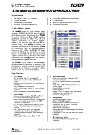
CC2430
    A True System-on-Chip solution for 2.4 GHz IEEE 802.15.4 / ZigBee®
Applications
•    2.4 GHz IEEE 802.15.4 systems                            •    Low power wireless sensor networks
•    ZigBee® systems                                          •    PC peripherals
•    Home/building automation                                 •    Set-top boxes and remote controls
•    Industrial Control and Monitoring                        •    Consumer Electronics

Product Description
The CC2430 comes in three different flash
versions: CC2430F32/64/128, with 32/64/128
KB of flash memory respectively. The CC2430
is a true System-on-Chip (SoC) solution
specifically tailored for IEEE 802.15.4 and
ZigBee® applications. It enables ZigBee®
nodes to be built with very low total bill-of-
material costs. The CC2430 combines the
excellent performance of the leading CC2420
RF transceiver with an industry-standard
enhanced 8051 MCU, 32/64/128 KB flash
memory, 8 KB RAM and many other powerful
features. Combined with the industry leading
ZigBee® protocol stack (Z-Stack™) from Texas
Instruments, the CC2430 provides the market’s
most competitive ZigBee® solution.
The CC2430 is highly suited for systems where
ultra low power consumption is required. This
is ensured by various operating modes. Short
transition times between operating modes
further ensure low power consumption.

Key Features
•     RF/Layout                                               •       Microcontroller
    o 2.4 GHz IEEE 802.15.4 compliant RF                          o High performance and low power 8051
      transceiver (industry leading CC2420 radio                    microcontroller core
      core)                                                       o 32, 64 or 128 KB in-system programmable
    o Excellent receiver sensitivity and robustness to              flash
      interferers                                                 o 8 KB RAM, 4 KB with data retention in all
    o Very few external components                                  power modes
    o Only a single crystal needed for mesh network               o Powerful DMA functionality
      systems                                                     o Watchdog timer
    o RoHS compliant 7x7mm QLP48 package                          o One IEEE 802.15.4 MAC timer, one general
                                                                    16-bit timer and two 8-bit timers
•     Low Power                                                   o Hardware debug support
    o Low current consumption (RX: 27 mA, TX: 27
      mA, microcontroller running at 32 MHz)                  •       Peripherals
    o Only 0.5 µA current consumption in powerdown                o CSMA/CA hardware support.
      mode, where external interrupts or the RTC                  o Digital RSSI / LQI support
      can wake up the system                                      o Battery monitor and temperature sensor
    o 0.3 µA current consumption in stand-by mode,                o 12-bit ADC with up to eight inputs and
      where external interrupts can wake up the                     configurable resolution
      system                                                      o AES security coprocessor
    o Very fast transition times from low-power                   o Two powerful USARTs with support for several
      modes to active mode enables ultra low                        serial protocols
      average power consumption in low dutycycle                  o 21 general I/O pins, two with 20mA sink/source
      systems                                                       capability
    o Wide supply voltage range (2.0V - 3.6V)
                                                              •       Development tools
                                                                  o Powerful and flexible development tools
                                                                    available


                                           CC2430 Data Sheet (rev. 2.1) SWRS036F                 Page 1 of 211
CC2430
Table Of Contents
1     ABBREVIATIONS................................................................................................................................ 5
2     REFERENCES....................................................................................................................................... 7
3     REGISTER CONVENTIONS .............................................................................................................. 8
4     FEATURES EMPHASIZED ................................................................................................................ 9
  4.1 HIGH-PERFORMANCE AND LOW-POWER 8051-COMPATIBLE MICROCONTROLLER ............................... 9
  4.2 UP TO 128 KB NON-VOLATILE PROGRAM MEMORY AND 2 X 4 KB DATA MEMORY ............................ 9
  4.3 HARDWARE AES ENCRYPTION/DECRYPTION ....................................................................................... 9
  4.4 PERIPHERAL FEATURES ......................................................................................................................... 9
  4.5 LOW POWER.......................................................................................................................................... 9
  4.6 IEEE 802.15.4 MAC HARDWARE SUPPORT ........................................................................................... 9
  4.7 INTEGRATED 2.4GHZ DSSS DIGITAL RADIO ........................................................................................ 9
5     ABSOLUTE MAXIMUM RATINGS ................................................................................................ 10
6     OPERATING CONDITIONS............................................................................................................. 10
7     ELECTRICAL SPECIFICATIONS .................................................................................................. 11
  7.1 GENERAL CHARACTERISTICS .............................................................................................................. 12
  7.2 RF RECEIVE SECTION ......................................................................................................................... 13
  7.3 RF TRANSMIT SECTION ....................................................................................................................... 13
  7.4 32 MHZ CRYSTAL OSCILLATOR .......................................................................................................... 14
  7.5 32.768 KHZ CRYSTAL OSCILLATOR .................................................................................................... 14
  7.6 32 KHZ RC OSCILLATOR..................................................................................................................... 15
  7.7 16 MHZ RC OSCILLATOR ................................................................................................................... 15
  7.8 FREQUENCY SYNTHESIZER CHARACTERISTICS ................................................................................... 16
  7.9 ANALOG TEMPERATURE SENSOR ........................................................................................................ 16
  7.10 ADC ................................................................................................................................................... 16
  7.11 CONTROL AC CHARACTERISTICS........................................................................................................ 18
  7.12 SPI AC CHARACTERISTICS ................................................................................................................. 19
  7.13 DEBUG INTERFACE AC CHARACTERISTICS ......................................................................................... 20
  7.14 PORT OUTPUTS AC CHARACTERISTICS ............................................................................................... 21
  7.15 TIMER INPUTS AC CHARACTERISTICS................................................................................................. 21
  7.16 DC CHARACTERISTICS ........................................................................................................................ 21
8     PIN AND I/O PORT CONFIGURATION ........................................................................................ 22
9     CIRCUIT DESCRIPTION ................................................................................................................. 24
  9.1 CPU AND PERIPHERALS ...................................................................................................................... 25
  9.2 RADIO ................................................................................................................................................. 26
10    APPLICATION CIRCUIT ................................................................................................................. 27
  10.1 INPUT / OUTPUT MATCHING ................................................................................................................. 27
  10.2 BIAS RESISTORS .................................................................................................................................. 27
  10.3 CRYSTAL ............................................................................................................................................. 27
  10.4 VOLTAGE REGULATORS ...................................................................................................................... 27
  10.5 DEBUG INTERFACE .............................................................................................................................. 27
  10.6 POWER SUPPLY DECOUPLING AND FILTERING...................................................................................... 28
11    8051 CPU .............................................................................................................................................. 30
  11.1 8051 CPU INTRODUCTION .................................................................................................................. 30
  11.2 MEMORY ............................................................................................................................................. 30
  11.3 CPU REGISTERS .................................................................................................................................. 42
  11.4 INSTRUCTION SET SUMMARY .............................................................................................................. 44
  11.5 INTERRUPTS ........................................................................................................................................ 49
12    DEBUG INTERFACE......................................................................................................................... 60
  12.1 DEBUG MODE ..................................................................................................................................... 60
  12.2 DEBUG COMMUNICATION ................................................................................................................... 60
  12.3 DEBUG COMMANDS ............................................................................................................................ 60
  12.4 DEBUG LOCK BIT ................................................................................................................................ 60
  12.5 DEBUG INTERFACE AND POWER MODES ............................................................................................. 64
13    PERIPHERALS ................................................................................................................................... 65


                                                 CC2430 Data Sheet (rev. 2.1) SWRS036F                                                    Page 2 of 211
CC2430
  13.1 POWER MANAGEMENT AND CLOCKS ................................................................................................... 65
  13.2 RESET ................................................................................................................................................. 71
  13.3 FLASH CONTROLLER ........................................................................................................................... 71
  13.4 I/O PORTS ............................................................................................................................................ 77
  13.5 DMA CONTROLLER ............................................................................................................................ 88
  13.6 16-BIT TIMER, TIMER1 ........................................................................................................................ 99
  13.7 MAC TIMER (TIMER2)...................................................................................................................... 110
  13.8 8-BIT TIMERS, TIMER 3 AND TIMER 4 ................................................................................................ 117
  13.9 SLEEP TIMER ..................................................................................................................................... 126
  13.10 ADC ................................................................................................................................................. 128
  13.11 RANDOM NUMBER GENERATOR ....................................................................................................... 134
  13.12 AES COPROCESSOR .......................................................................................................................... 136
  13.13 WATCHDOG TIMER ........................................................................................................................... 141
  13.14 USART............................................................................................................................................. 143
14    RADIO ................................................................................................................................................ 153
  14.1 IEEE 802.15.4 MODULATION FORMAT ............................................................................................. 154
  14.2 COMMAND STROBES ......................................................................................................................... 155
  14.3 RF REGISTERS................................................................................................................................... 155
  14.4 INTERRUPTS ...................................................................................................................................... 155
  14.5 FIFO ACCESS .................................................................................................................................... 157
  14.6 DMA ................................................................................................................................................ 157
  14.7 RECEIVE MODE.................................................................................................................................. 158
  14.8 RXFIFO OVERFLOW ......................................................................................................................... 158
  14.9 TRANSMIT MODE ............................................................................................................................... 159
  14.10 GENERAL CONTROL AND STATUS ...................................................................................................... 160
  14.11 DEMODULATOR, SYMBOL SYNCHRONIZER AND DATA DECISION ..................................................... 160
  14.12 FRAME FORMAT ................................................................................................................................ 161
  14.13 SYNCHRONIZATION HEADER ............................................................................................................. 161
  14.14 LENGTH FIELD ................................................................................................................................... 162
  14.15 MAC PROTOCOL DATA UNIT ............................................................................................................. 162
  14.16 FRAME CHECK SEQUENCE ................................................................................................................. 162
  14.17 RF DATA BUFFERING ........................................................................................................................ 163
  14.18 ADDRESS RECOGNITION .................................................................................................................... 164
  14.19 ACKNOWLEDGE FRAMES .................................................................................................................. 165
  14.20 RADIO CONTROL STATE MACHINE ..................................................................................................... 166
  14.21 MAC SECURITY OPERATIONS (ENCRYPTION AND AUTHENTICATION).............................................. 168
  14.22 LINEAR IF AND AGC SETTINGS ........................................................................................................ 168
  14.23 RSSI / ENERGY DETECTION .............................................................................................................. 168
  14.24 LINK QUALITY INDICATION .............................................................................................................. 168
  14.25 CLEAR CHANNEL ASSESSMENT......................................................................................................... 169
  14.26 FREQUENCY AND CHANNEL PROGRAMMING ..................................................................................... 169
  14.27 VCO AND PLL SELF-CALIBRATION .................................................................................................. 169
  14.28 OUTPUT POWER PROGRAMMING ....................................................................................................... 170
  14.29 INPUT / OUTPUT MATCHING .............................................................................................................. 170
  14.30 TRANSMITTER TEST MODES ............................................................................................................. 171
  14.31 SYSTEM CONSIDERATIONS AND GUIDELINES .................................................................................... 173
  14.32 PCB LAYOUT RECOMMENDATION .................................................................................................... 175
  14.33 ANTENNA CONSIDERATIONS ............................................................................................................. 175
  14.34 CSMA/CA STROBE PROCESSOR ....................................................................................................... 176
  14.35 RADIO REGISTERS ............................................................................................................................. 183
15    VOLTAGE REGULATORS............................................................................................................. 202
  15.1 VOLTAGE REGULATORS POWER-ON.................................................................................................. 202
16    EVALUATION SOFTWARE........................................................................................................... 202
17    REGISTER OVERVIEW ................................................................................................................. 203
18    PACKAGE DESCRIPTION (QLP 48) ............................................................................................ 206
  18.1 RECOMMENDED PCB LAYOUT FOR PACKAGE (QLP 48).................................................................... 207
  18.2 PACKAGE THERMAL PROPERTIES....................................................................................................... 207
  18.3 SOLDERING INFORMATION ................................................................................................................ 207
  18.4 TRAY SPECIFICATION ........................................................................................................................ 207


                                                 CC2430 Data Sheet (rev. 2.1) SWRS036F                                                    Page 3 of 211
CC2430
  18.5 CARRIER TAPE AND REEL SPECIFICATION .......................................................................................... 207
19    ORDERING INFORMATION......................................................................................................... 209
20    GENERAL INFORMATION ........................................................................................................... 210
  20.1 DOCUMENT HISTORY ........................................................................................................................ 210
21    ADDRESS INFORMATION ............................................................................................................ 210
22    TI WORLDWIDE TECHNICAL SUPPORT ................................................................................. 210


                                             CC2430 Data Sheet (rev. 2.1) SWRS036F                                            Page 4 of 211
CC2430
1     Abbreviations
ADC         Analog to Digital Converter                      I/O          Input / Output
AES         Advanced Encryption Standard                     I/Q          In-phase / Quadrature-phase
AGC         Automatic Gain Control                           IEEE         Institute of Electrical and Electronics
                                                                          Engineers
ARIB        Association of Radio Industries and
            Businesses                                       IF           Intermediate Frequency
BCD         Binary Coded Decimal                             INL          Integral Nonlinearity
BER         Bit Error Rate                                   IOC          I/O Controller
BOD         Brown Out Detector                               IRQ          Interrupt Request
BOM         Bill of Materials                                ISM          Industrial, Scientific and Medical
CBC         Cipher Block Chaining                            ITU-T        International Telecommunication Union
                                                                          – Telecommunication Standardization
CBC-MAC     Cipher Block Chaining Message                                 Sector
            Authentication Code
                                                             IV           Initialization Vector
CCA         Clear Channel Assessment
                                                             JEDEC        Joint Electron Device Engineering
CCM         Counter mode + CBC-MAC                                        Council
CFB         Cipher Feedback                                  KB           1024 bytes
CFR         Code of Federal Regulations                      kbps         kilo bits per second
CMOS        Complementary Metal Oxide                        LC           Inductor-capacitor
            Semiconductor
                                                             LFSR         Linear Feedback Shift Register
CMRR        Common Mode Ratio Recjection
                                                             LNA          Low-Noise Amplifier
CPU         Central Processing Unit
                                                             LO           Local Oscillator
CRC         Cyclic Redundancy Check
                                                             LQI          Link Quality Indication
CSMA-CA     Carrier Sense Multiple Access with
            Collision Avoidance                              LSB          Least Significant Bit / Byte
CSP         CSMA/CA Strobe Processor                         LSB          Least Significant Byte
CTR         Counter mode (encryption)                        MAC          Medium Access Control
CW          Continuous Wave                                  MAC          Message Authentication Code
DAC         Digital to Analog Converter                      MCU          Microcontroller Unit
DC          Direct Current                                   MFR          MAC Footer
DMA         Direct Memory Access                             MHR          MAC Header
DNL         Differential Nonlineraity                        MIC          Message Integrity Code
DSM         Delta Sigma Modulator                            MISO         Master In Slave Out
DSSS        Direct Sequence Spread Spectrum                  MOSI         Master Out Slave In
ECB         Electronic Code Book (encryption)                MPDU         MAC Protocol Data Unit
EM          Evaluation Module                                MSB          Most Significant Byte
ENOB        Effective Number of bits                         MSDU         MAC Service Data Unit
ESD         Electro Static Discharge                         MUX          Multiplexer
ESR         Equivalent Series Resistance                     NA           Not Available
ETSI        European Telecommunications                      NC           Not Connected
            Standards Institute
                                                             OFB          Output Feedback (encryption)
EVM         Error Vector Magnitude
                                                             O-QPSK       Offset - Quadrature Phase Shift Keying
FCC         Federal Communications Commission
                                                             PA           Power Amplifier
FCF         Frame Control Field
                                                             PCB          Printed Circuit Board
FCS         Frame Check Sequence
                                                             PER          Packet Error Rate
FFCTRL      FIFO and Frame Control
                                                             PHR          PHY Header
FIFO        First In First Out
                                                             PHY          Physical Layer
HF          High Frequency
                                                             PLL          Phase Locked Loop
HSSD        High Speed Serial Data


                                  CC2430 Data Sheet (rev. 2.1) SWRS036F                           Page 5 of 211
CC2430
PM{0-3}   Power Mode 0-3                                  SPI          Serial Peripheral Interface
PMC       Power Management Controller                     SRAM         Static Random Access Memory
POR       Power On Reset                                  ST           Sleep Timer
PSDU      PHY Service Data Unit                           T/R          Tape and reel
PWM       Pulse Width Modulator                           T/R          Transmit / Receive
QLP       Quad Leadless Package                           TBD          To Be Decided / To Be Defined
RAM       Random Access Memory                            THD          Total Harmonic Distortion
RBW       Resolution Bandwidth                            TI           Texas Instruments
RC        Resistor-Capacitor                              TX           Transmit
RCOSC     RC Oscillator                                   UART         Universal Asynchronous
                                                                       Receiver/Transmitter
RF        Radio Frequency
                                                          USART        Universal Synchronous/Asynchronous
RoHS      Restriction on Hazardous Substances                          Receiver/Transmitter
RSSI      Receive Signal Strength Indicator               VCO          Voltage Controlled Oscillator
RTC       Real-Time Clock                                 VGA          Variable Gain Amplifier
RX        Receive                                         WDT          Watchdog Timer
SCK       Serial Clock                                    XOSC         Crystal Oscillator
SFD       Start of Frame Delimiter
SFR       Special Function Register
SHR       Synchronization Header
SINAD     Signal-to-noise and distortion ratio


                               CC2430 Data Sheet (rev. 2.1) SWRS036F                        Page 6 of 211
CC2430
2     References
[1]   IEEE std. 802.15.4 - 2003: Wireless Medium Access Control (MAC) and Physical Layer (PHY)
        specifications for Low Rate Wireless Personal Area Networks (LR-WPANs)
        http://standards.ieee.org/getieee802/download/802.15.4-2003.pdf
[2]   NIST FIPS Pub 197: Advanced Encryption Standard (AES), Federal Information Processing Standards
        Publication 197, US Department of Commerce/N.I.S.T., November 26, 2001. Available from the NIST
        website.

        http://csrc.nist.gov/publications/fips/fips197/fips-197.pdf


                               CC2430 Data Sheet (rev. 2.1) SWRS036F                  Page 7 of 211
CC2430
3   Register conventions
Each SFR register is described in a separate           REGISTER NAME (XDATA Address)
table. The table heading is given in the
                                                       In the register descriptions, each register bit is
following format:
                                                       shown with a symbol indicating the access
REGISTER NAME (SFR Address) - Register                 mode of the register bit. The register values
Description.                                           are always given in binary notation unless
                                                       prefixed by ‘0x’ which indicates hexadecimal
Each RF register is described in a separate
                                                       notation.
table. The table heading is given in the
following format:
                               Table 1: Register bit conventions
                Symbol                         Access Mode

                R/W                            Read/write
                R                              Read only
                R0                             Read as 0

                R1                             Read as 1

                W                              Write only
                W0                             Write as 0

                W1                             Write as 1
                H0                             Hardware clear

                H1                             Hardware set


                            CC2430 Data Sheet (rev. 2.1) SWRS036F                      Page 8 of 211
CC2430
4       Features Emphasized
4.1      High-Performance and Low-Power                   4.5    Low Power
         8051-Compatible Microcontroller
                                                            •    Four flexible power modes for reduced
    • Optimized 8051 core, which typically                       power consumption
      gives 8x the performance of a standard                •    System can wake up on external
      8051                                                       interrupt or real-time counter event
    • Dual data pointers                                    •    Low-power fully static CMOS design
    • In-circuit interactive debugging is                   •    System clock source can be 16 MHz RC
      supported for the IAR Embedded                             oscillator or 32 MHz crystal oscillator.
      Workbench through a simple two-wire                        The 32 MHz oscillator is used when
      serial interface                                           radio is active
4.2      Up to 128 KB Non-volatile Program                  •    Optional clock source for ultra-low power
         Memory and 2 x 4 KB Data Memory                         operation can be either low-power RC
                                                                 oscillator or an optional 32.768 kHz
    •   32/64/128 KB of non-volatile flash                       crystal oscillator
        memory      in-system     programmable
        through a simple two-wire interface or by         4.6    IEEE 802.15.4 MAC hardware support
        the 8051 core
                                                            •    Automatic preamble generator
    •   Worst-case flash memory endurance:
        1000 write/erase cycles                             •    Synchronization word insertion/detection
    •   Programmable read and write lock of                 •    CRC-16 computation and checking over
        portions of Flash memory for software                    the MAC payload
        security                                            •    Clear Channel Assessment
    •   4096 bytes of internal SRAM with data               •    Energy detection / digital RSSI
        retention in all power modes                        •    Link Quality Indication
    •   Additional 4096 bytes of internal SRAM              •    CSMA/CA Coprocessor
        with data retention in power modes 0
        and 1                                             4.7    Integrated 2.4GHz DSSS Digital Radio
4.3      Hardware AES Encryption/Decryption                 •    2.4 GHz IEEE 802.15.4 compliant RF
                                                                 transceiver (based on industry leading
    •   AES supported in hardware coprocessor                    CC2420 radio core).
4.4      Peripheral Features                                •    Excellent receiver sensitivity            and
                                                                 robustness to interferers
    •   Powerful DMA Controller                             •    250 kbps data rate, 2 MChip/s chip rate
    •   Power On Reset/Brown-Out Detection                  •    Reference    designs   comply      with
    •   Eight channel ADC with configurable                      worldwide radio frequency regulations
        resolution                                               covered by ETSI EN 300 328 and EN
    •   Programmable watchdog timer                              300 440 class 2 (Europe), FCC CFR47
                                                                 Part 15 (US) and ARIB STD-T66
    •   Real time clock with 32.768 kHz crystal                  (Japan). Transmit on 2480MHz under
        oscillator                                               FCC is supported by duty-cycling, or by
    •   Four timers: one general 16-bit timer,                   reducing output power.
        two general 8-bit timers, one MAC timer
    •   Two    programmable     USARTs     for
        master/slave SPI or UART operation
    •   21 configurable general-purpose digital
        I/O-pins
    •   True random number generator


                                CC2430 Data Sheet (rev. 2.1) SWRS036F                      Page 9 of 211
CC2430
5     Absolute Maximum Ratings
Under no circumstances must the absolute maximum ratings given in Table 2 be violated. Stress
exceeding one or more of the limiting values may cause permanent damage to the device.
                                    Table 2: Absolute Maximum Ratings
Parameter                               Min            Max            Units      Condition

Supply voltage                          –0.3            3.9             V        All supply pins must have the same voltage
Voltage on any digital pin              –0.3         VDD+0.3,           V
                                                      max 3.9
Voltage on the 1.8V pins (pin no.       –0.3            2.0             V
22, 25-40 and 42)
Input RF level                                            10           dBm

Storage temperature range               –50            150             °C        Device not programmed

Reflow soldering temperature                           260             °C        According to IPC/JEDEC J-STD-020C

                                                                                 On RF pads (RF_P, RF_N, AVDD_RF1,
                                                       <500             V        and AVDD_RF2), according to Human
                                                                                 Body Model, JEDEC STD 22, method A114
ESD                                                                              All other pads, according to Human Body
                                                       700              V
                                                                                 Model, JEDEC STD 22, method A114
                                                                                 According to Charged Device Model,
                                                       200              V
                                                                                 JEDEC STD 22, method C101

                                    Caution! ESD sensitive device. Precaution should be used
                                             when handling the device in order to prevent
                                             permanent damage.


6     Operating Conditions
The operating conditions for CC2430 are listed in Table 3 .
                                       Table 3: Operating Conditions
 Parameter                              Min          Max        Unit        Condition
 Operating ambient temperature          -40          85          °C
 range, TA
 Operating supply voltage               2.0          3.6         V          The supply pins to the radio part must be driven
                                                                            by the 1.8 V on-chip regulator


                                    CC2430 Data Sheet (rev. 2.1) SWRS036F                                Page 10 of 211
CC2430
7         Electrical Specifications
Measured on Texas Instruments CC2430 EM reference design with TA=25°C and VDD=3.0V
unless stated otherwise.
                                    Table 4: Electrical Specifications
    Parameter                      Min   Typ    Max    Unit   Condition

    Current Consumption
                                                              Digital regulator on. 16 MHz RCOSC running. No radio,
    MCU Active Mode, 16 MHz,                                  crystals, or peripherals active.
                                         4.3           mA
    low MCU activity                                          Low MCU activity: no flash access (i.e. only cache hit),
                                                              no RAM access.
                                                              Digital regulator on. 16 MHz RCOSC running. No radio,
    MCU Active Mode, 16 MHz,                                  crystals, or peripherals active.
                                         5.1           mA
    medium MCU activity                                                                               1
                                                              Medium MCU activity: normal flash access , minor RAM
                                                              access.
                                                              Digital regulator on. 16 MHz RCOSC running. No radio,
    MCU Active Mode, 16 MHz,                                  crystals, or peripherals active.
                                         5.7           mA
    high MCU activity                                                                               1
                                                              High MCU activity: normal flash access , extensive RAM
                                                              access and heavy CPU load.
                                                              32 MHz XOSC running. No radio or peripherals active.
    MCU Active Mode, 32 MHz,
                                         9.5           mA     Low MCU activity : no flash access (i.e. only cache hit),
    low MCU activity
                                                              no RAM access
                                                              32 MHz XOSC running. No radio or peripherals active.
    MCU Active Mode, 32 MHz,
                                         10.5          mA                                             1
                                                              Medium MCU activity: normal flash access , minor RAM
    medium MCU activity
                                                              access.
                                                              32 MHz XOSC running. No radio or peripherals active.
    MCU Active Mode, 32 MHz,
                                         12.3          mA                                           1
                                                              High MCU activity: normal flash access , extensive RAM
    high MCU activity
                                                              access and heavy CPU load.
                                                              MCU running at full speed (32MHz), 32MHz XOSC
    MCU Active and RX Mode               26.7          mA     running, radio in RX mode, -50 dBm input power. No
                                                              peripherals active. Low MCU activity.
                                                              MCU running at full speed (32MHz), 32MHz XOSC
    MCU Active and TX Mode, 0dBm         26.9          mA     running, radio in TX mode, 0dBm output power. No
                                                              peripherals active. Low MCU activity.
                                                              Digital regulator on, 16 MHz RCOSC and 32 MHz crystal
    Power mode 1                         190           µA     oscillator off. 32.768 kHz XOSC, POR and ST active.
                                                              RAM retention.
                                                              Digital regulator off, 16 MHz RCOSC and 32 MHz crystal
    Power mode 2                         0.5           µA     oscillator off. 32.768 kHz XOSC, POR and ST active.
                                                              RAM retention.
    Power mode 3                         0.3           µA     No clocks. RAM retention. POR active.
    Peripheral Current                                        Adds to the figures above if the peripheral unit is
    Consumption                                               activated
    Timer 1                              150           µA     Timer running, 32MHz XOSC used.

    Timer 2                              230           µA     Timer running, 32MHz XOSC used.

    Timer 3                              50            µA     Timer running, 32MHz XOSC used.

    Timer 4                              50            µA     Timer running, 32MHz XOSC used.

    Sleep Timer                          0.2           µA     Including 32.753 kHz RCOSC.

    ADC                                  1.2           mA     When converting.
    Flash write                           3            mA     Estimated value
    Flash erase                           3            mA     Estimated value


1
  Normal Flash access means that the code used exceeds the cache storage (see last paragraph
in section 11.2.3 Flash memory) so cache misses will happen frequently.


                                   CC2430 Data Sheet (rev. 2.1) SWRS036F                             Page 11 of 211
CC2430
7.1       General Characteristics
Measured on Texas Instruments CC2430 EM reference design with TA=25°C and VDD=3.0V
unless stated otherwise.
                                      Table 5: General Characteristics
 Parameter                          Min      Typ      Max         Unit      Condition/Note

 Wake-Up and Timing
                                                                            Digital regulator on, 16 MHz RCOSC and
 Power mode 1      power
                                             4.1                   µs       32 MHz crystal oscillator off. Start-up of
 mode 0
                                                                            16 MHz RCOSC.
                                                                            Digital regulator off, 16 MHz RCOSC and
 Power mode 2 or 3      power
                                             120                   µs       32 MHz crystal oscillator off. Start-up of
 mode 0
                                                                            regulator and 16 MHz RCOSC.
                                                                            Time from enabling radio part in power
 Active   TX or RX
                                                                            mode 0, until TX or RX starts. Includes
 32MHz XOSC initially OFF.                   525                   µs
                                                                            start-up of voltage regulator and crystal
 Voltage regulator initially OFF
                                                                            oscillator in parallel. Crystal ESR=16Ω.
                                                                            Time from enabling radio part in power
 Active   TX or RX
                                             320                   µs       mode 0, until TX or RX starts. Includes
 Voltage regulator initially OFF
                                                                            start-up of voltage regulator.
                                                                            Radio part already enabled.
 Active     RX or TX                                   192         µs
                                                                            Time until RX or TX starts.

 RX/TX turnaround                                      192         µs

 Radio part
 RF Frequency Range                2400              2483.5     MHz         Programmable in 1 MHz steps, 5 MHz
                                                                            between channels for compliance with
                                                                            [1]
 Radio bit rate                             250                 kbps        As defined by [1]


 Radio chip rate                            2.0                 MChip/s     As defined by [1]


                                    CC2430 Data Sheet (rev. 2.1) SWRS036F                          Page 12 of 211
CC2430
7.2    RF Receive Section
Measured on Texas Instruments CC2430 EM reference design with TA=25°C and VDD=3.0V
unless stated otherwise.
                                Table 6: RF Receive Parameters
 Parameter                     Min   Typ    Max    Unit   Condition/Note
 Receiver sensitivity                 -92          dBm    PER = 1%, as specified by [1]
                                                          Measured in 50 Ω single endedly through a balun.
                                                          [1] requires –85 dBm
 Saturation (maximum input            10           dBm    PER = 1%, as specified by [1]
 level)                                                   Measured in 50 Ω single endedly through a balun.
                                                          [1] requires –20 dBm
 Adjacent channel rejection                               Wanted signal -88dBm, adjacent modulated channel
 + 5 MHz channel spacing              41            dB    at +5 MHz, PER = 1 %, as specified by [1].
                                                          [1] requires 0 dB
 Adjacent channel rejection                               Wanted signal -88dBm, adjacent modulated channel
 - 5 MHz channel spacing              30            dB    at -5 MHz, PER = 1 %, as specified by [1].
                                                          [1] requires 0 dB
 Alternate channel rejection                              Wanted signal -88dBm, adjacent modulated channel
 + 10 MHz channel spacing             55            dB    at +10 MHz, PER = 1 %, as specified by [1]
                                                          [1] requires 30 dB
 Alternate channel rejection                              Wanted signal -88dBm, adjacent modulated channel
 - 10 MHz channel spacing             53            dB    at -10 MHz, PER = 1 %, as specified by [1]
                                                          [1] requires 30 dB
 Channel rejection                                        Wanted signal @ -82 dBm. Undesired signal is an
 ≥ + 15 MHz                           55            dB    802.15.4 modulated channel, stepped through all
                                                          channels from 2405 to 2480 MHz. Signal level for
 ≤ - 15 MHz                           53            dB    PER = 1%. Values are estimated.
 Co-channel rejection                                     Wanted signal @ -82 dBm. Undesired signal is
                                      -6            dB    802.15.4 modulated at the same frequency as the
                                                          desired signal. Signal level for PER = 1%.
 Blocking / Desensitization
 + 5 MHz from band edge               -42          dBm    Wanted signal 3 dB above the sensitivity level, CW
 + 10 MHz from band edge              -45          dBm    jammer, PER = 1%. Measured according to EN 300
 + 20 MHz from band edge              -26          dBm    440 class 2.
 + 50 MHz from band edge              -22          dBm
 - 5 MHz from band edge               -31          dBm
 - 10 MHz from band edge              -36          dBm
 - 20 MHz from band edge              -24          dBm
 - 50 MHz from band edge              -25          dBm


 Spurious emission
 30 – 1000 MHz                              −64    dBm    Conducted measurement in a 50 Ω single ended
 1 – 12.75 GHz                              −75    dBm    load. Complies with EN 300 328, EN 300 440 class
                                                          2, FCC CFR47, Part 15 and ARIB STD-T-66.

 Frequency error tolerance           ±140          ppm    Difference between centre frequency of the received
                                                          RF signal and local oscillator frequency.
                                                          [1] requires minimum 80 ppm
 Symbol rate error tolerance         ±900          ppm    Difference between incoming symbol rate and the
                                                          internally generated symbol rate
                                                          [1] requires minimum 80 ppm


7.3    RF Transmit Section
Measured on Texas Instruments CC2430 EM reference design with TA=25°C, VDD=3.0V, and
nominal output power unless stated otherwise.


                               CC2430 Data Sheet (rev. 2.1) SWRS036F                          Page 13 of 211
CC2430
                                            Table 7: RF Transmit Parameters
    Parameter               Min     Typ          Max        Unit    Condition/Note
    Nominal output                     0                    dBm     Delivered to a single ended 50 Ω load through a balun and
    power                                                           output power control set to 0x5F (TXCTRLL).
                                                                    [1] requires minimum –3 dBm
    Programmable                    26                      dB      The output power is programmable in 16 steps from typically
    output power range                                              -25.2 to 0.6 dBm (see Table 45).

    Harmonics
        nd
    2 harmonic                     -50.7                    dBm     Measurement conducted with 100 kHz resolution bandwidth on
        rd
    3 harmonic                     -55.8                    dBm     spectrum analyzer and output power control set to 0x5F
        th                                                          (TXCTRLL). Output Delivered to a single ended 50 Ω load
    4        harmonic              -54.2                    dBm     through a balun.
        th
    5 harmonic                     -53.4                    dBm


    Spurious emission                                               Maximum output power.
    30 - 1000 MHz                   -47                     dBm     Texas Instruments CC2430 EM reference design complies with
                                                                    EN 300 328, EN 300 440, FCC CFR47 Part 15 and ARIB STD-
    1– 12.75 GHz                    -43                     dBm     T-66.
    1.8 – 1.9 GHz                   -58                     dBm     Transmit on 2480MHz under FCC is supported by duty-cycling,
    5.15 – 5.3 GHz                  -56                     dBm     or by reducing output power
                                                                    The peak conducted spurious emission is -47 dBm @ 192 MHz
                                                                    which is in an EN 300 440 restricted band limited to -54 dBm. All
                                                                    radiated spurious emissions are within the limits of
                                                                    ETSI/FCC/ARIB. Conducted spurious emission (CSE) can be
                                                                    reduced with a simple band pass filter connected between
                                                                    matching network and RF connector (1.8 pF in parallel with 1.6
                                                                    nH reduces the CSE by 20 dB), this filter must be connected to
                                                                    good RF ground.
    Error Vector                    11                      %       Measured as defined by [1]
    Magnitude (EVM)                                                 [1] requires max. 35 %
    Optimum load                     60                     Ω       Differential impedance as seen from the RF-port (RF_P and
    impedance                      + j164                           RF_N) towards the antenna2.

7.4            32 MHz Crystal Oscillator
Measured on Texas Instruments CC2430 EM reference design with TA=25°C and VDD=3.0V
unless stated otherwise.
                                  Table 8: 32 MHz Crystal Oscillator Parameters
    Parameter             Min     Typ       Max        Unit        Condition/Note
    Crystal frequency             32                   MHz
    Crystal frequency     - 40              40         ppm         Including aging and temperature dependency, as specified by [1]
    accuracy
    requirement
    ESR                    6      16        60          Ω          Simulated over operating conditions

    C0                     1      1.9        7         pF          Simulated over operating conditions
    CL                     10     13        16         pF          Simulated over operating conditions
    Start-up time                 212                  µs


7.5            32.768 kHz Crystal Oscillator
Measured on Texas Instruments CC2430 EM reference design with TA=25°C and VDD=3.0V
unless stated otherwise.

2
    This is for 2440MHz


                                           CC2430 Data Sheet (rev. 2.1) SWRS036F                                     Page 14 of 211
CC2430
                                  Table 9: 32.768 kHz Crystal Oscillator Parameters
 Parameter                  Min     Typ       Max         Unit     Condition/Note
 Crystal frequency                 32.768                 kHz
 Crystal frequency          –40                40         ppm      Including aging and temperature dependency, as specified by [1]
 accuracy
 requirement
 ESR                                 40       130         kΩ       Simulated over operating conditions

 C0                                  0.9      2.0         pF       Simulated over operating conditions
 CL                                  12        16         pF       Simulated over operating conditions
 Start-up time                       400                  ms       Value is simulated.


7.6     32 kHz RC Oscillator
Measured on Texas Instruments CC2430 EM reference design with TA=25°C and VDD=3.0V
unless stated otherwise.
                                     Table 10: 32 kHz RC Oscillator parameters
 Parameter                            Min        Typ             Max     Unit        Condition/Note
 Calibrated frequency                          32.753                    kHz         The calibrated 32 kHz RC Oscillator frequency
                                                                                     is the 32 MHz XTAL frequency divided by 977
 Frequency accuracy after                       ±0.2                     %           Value is estimated.
 calibration
 Temperature coefficient                        +0.4                     % / °C      Frequency drift when temperature changes
                                                                                     after calibration. Value is estimated.
 Supply voltage coefficient                         +3                  %/V          Frequency drift when supply voltage changes
                                                                                     after calibration. Value is estimated.
 Initial calibration time                           1.7                  ms          When the 32 kHz RC Oscillator is enabled,
                                                                                     calibration is continuously done in the
                                                                                     background as long as the 32 MHz crystal
                                                                                     oscillator is running and
                                                                                     SLEEP.OSC32K_CALDIS bit is cleared.


7.7     16 MHz RC Oscillator
Measured on Texas Instruments CC2430 EM reference design with TA=25°C and VDD=3.0V
unless stated otherwise.
                                     Table 11: 16 MHz RC Oscillator parameters
 Parameter                            Min        Typ             Max     Unit        Condition/Note
 Frequency                                          16                   MHz         The calibrated 16 MHz RC Oscillator
                                                                                     frequency is the 32 MHz XTAL frequency
                                                                                     divided by 2
 Uncalibrated frequency                          ±18                     %
 accuracy
 Calibrated frequency                           ±0.6             ±1      %
 accuracy
 Start-up time                                                   10      µs
 Temperature coefficient                                         -325    ppm / °C    Frequency drift when temperature changes
                                                                                     after calibration
 Supply voltage coefficient                                      28      ppm / mV    Frequency drift when supply voltage changes
                                                                                     after calibration
 Initial calibration time                           50                   µs          When the 16 MHz RC Oscillator is enabled it
                                                                                     will be calibrated continuously when the
                                                                                     32MHz crystal oscillator is running.


                                           CC2430 Data Sheet (rev. 2.1) SWRS036F                                   Page 15 of 211
CC2430
7.8       Frequency Synthesizer Characteristics
Measured on Texas Instruments CC2430 EM reference design with TA=25°C and VDD=3.0V
unless stated otherwise.
                                    Table 12: Frequency Synthesizer Parameters
    Parameter               Min       Typ              Max        Unit              Condition/Note

    Phase noise                                                                     Unmodulated carrier
                                      −116                        dBc/Hz            At ±1.5 MHz offset from carrier
                                      −117                        dBc/Hz            At ±3 MHz offset from carrier
                                      −118                        dBc/Hz            At ±5 MHz offset from carrier


    PLL lock time                                      192        µs                The startup time until RX/TX turnaround. The crystal
                                                                                    oscillator is running.


7.9       Analog Temperature Sensor
Measured on Texas Instruments CC2430 EM reference design with TA=25°C and VDD=3.0V
unless stated otherwise.
                                  Table 13: Analog Temperature Sensor Parameters
    Parameter                         Min        Typ         Max         Unit         Condition/Note

    Output voltage at –40°C                      0.648                   V            Value is estimated

    Output voltage at 0°C                        0.743                   V            Value is estimated

    Output voltage at +40°C                      0.840                   V            Value is estimated

    Output voltage at +80°C                      0.939                   V            Value is estimated

    Temperature coefficient                      2.45                    mV/°C        Fitted from –20°C to +80°C on estimated values.
    Absolute error in calculated                  –8                     °C           From –20°C to +80°C when assuming best fit for
    temperature                                                                       absolute accuracy on estimated values: 0.743V at
                                                                                      0°C and 2.45mV / °C.
    Error in calculated               -2           0          2          °C           From –20°C to +80°C when using 2.45mV / °C,
    temperature, calibrated                                                           after 1-point calibration at room temperature.
                                                                                      Values are estimated. Indicated min/max with 1-
                                                                                      point calibration is based on simulated values for
                                                                                      typical process parameters
    Current consumption                           280                    µA
    increase when enabled


7.10 ADC
Measured with TA=25°C and VDD=3.0V. Note that other data may result using Texas Instruments
CC2430 EM reference design.
                                                Table 14: ADC Characteristics
    Parameter                           Min        Typ        Max            Unit     Condition/Note

    Input voltage                           0                 VDD            V        VDD is voltage on AVDD_SOC pin
    External reference voltage              0                 VDD            V        VDD is voltage on AVDD_SOC pin
    External reference voltage              0                 VDD            V        VDD is voltage on AVDD_SOC pin
    differential
    Input resistance, signal                       197                       kΩ       Simulated using 4 MHz clock speed (see section
                                                                                      13.10.2.7)
                     3
    Full-Scale Signal                              2.97                      V        Peak-to-peak, defines 0dBFS


3
    Measured with 300 Hz Sine input and VDD as reference.


                                           CC2430 Data Sheet (rev. 2.1) SWRS036F                                           Page 16 of 211
CC2430
Parameter                           Min   Typ     Max    Unit   Condition/Note
              3
ENOB                                      5.7            bits   7-bits setting.
Single ended input                        7.5                   9-bits setting.
                                          9.3                   10-bits setting.
                                          10.8                  12-bits setting.
              3
ENOB                                      6.5            bits   7-bits setting.
Differential input                        8.3                   9-bits setting.
                                          10.0                  10-bits setting.
                                          11.5                  12-bits setting.
Useful Power Bandwidth                    0-20           kHz    7-bits setting, both single and differential
          3
THD
-Single ended input                       -75.2          dB     12-bits setting, -6dBFS
-Differential input                       -86.6          dB     12-bits setting, -6dBFS
                                3
Signal To Non-Harmonic Ratio
-Single ended input                       70.2           dB     12-bits setting
-Differential input                       79.3           dB     12-bits setting
                                3
Spurious Free Dynamic Range
-Single ended input                       78.8           dB     12-bits setting, -6dBFS
-Differential input                       88.9           dB     12-bits setting, -6dBFS
CMRR, differential input                  <-84           dB     12- bit setting, 1 kHz Sine (0dBFS), limited by ADC
                                                                resolution
Crosstalk, single ended input             <-84           dB     12- bit setting, 1 kHz Sine (0dBFS), limited by ADC
                                                                resolution
Offset                                     -3            mV     Mid. scale
Gain error                                0.68           %
          3
DNL                                       0.05           LSB    12-bits setting, mean
                                          0.9            LSB    12-bits setting, max
      3
INL                                       4.6            LSB    12-bits setting, mean
                                          13.3           LSB    12-bits setting, max
              3
SINAD                                     35.4           dB     7-bits setting.
Single ended input                        46.8           dB     9-bits setting.
(-THD+N)                                  57.5           dB     10-bits setting.
                                          66.6           dB     12-bits setting.
              3
SINAD                                     40.7           dB     7-bits setting.
Differential input                        51.6           dB     9-bits setting.
(-THD+N)                                  61.8           dB     10-bits setting.
                                          70.8           dB     12-bits setting.
Conversion time                            20            µs     7-bits setting.
                                           36            µs     9-bits setting.
                                           68            µs     10-bits setting.
                                          132            µs     12-bits setting.

Power Consumption                         1.2            mA


                                    CC2430 Data Sheet (rev. 2.1) SWRS036F                              Page 17 of 211
CC2430
7.11 Control AC Characteristics
TA= -40°C to 85°C, VDD=2.0V to 3.6V if nothing else stated.
                                 Table 15: Control Inputs AC Characteristics
 Parameter              Min        Typ     Max     Unit       Condition/Note

 System clock,           16                 32     MHz        System clock is 32 MHz when crystal oscillator is used.
 fSYSCLK                                                      System clock is 16 MHz when calibrated 16 MHz RC
 tSYSCLK= 1/ fSYSCLK                                          oscillator is used.

 RESET_N low            250                        ns         See item 1, Figure 1. This is the shortest pulse that is
 width                                                        guaranteed to be recognized as a complete reset pin
                                                              request. Note that shorter pulses may be recognized but
                                                              will not lead to complete reset of all modules within the
                                                              chip.
 Interrupt pulse       tSYSCLK                     ns         See item 2, Figure 1.This is the shortest pulse that is
 width                                                        guaranteed to be recognized as an interrupt request. In
                                                              PM2/3 the internal synchronizers are bypassed so this
                                                              requirement does not apply in PM2/3.


                                                          1
                       RESET_N


                       Px.n                               2


                                                          2


                       Px.n


                                 Figure 1: Control Inputs AC Characteristics


                                    CC2430 Data Sheet (rev. 2.1) SWRS036F                            Page 18 of 211
CC2430
7.12 SPI AC Characteristics
TA= -40°C to 85°C, VDD=2.0V to 3.6V if nothing else stated.
                                  Table 16: SPI AC Characteristics
 Parameter           Min        Typ      Max   Unit      Condition/Note

 SCK period                     See            ns        Master. See item 1 Figure 2
                               section
                               13.14.4
 SCK duty cycle                 50%                      Master.

 SSN low to SCK    2*tSYSCLK                             See item 5 Figure 2
 SCK to SSN high      30                       ns        See item 6 Figure 2
 MISO setup           10                       ns        Master. See item 2 Figure 2
 MISO hold            10                       ns        Master. See item 3 Figure 2
 SCK to MOSI                             25    ns        Master. See item 4 Figure 2, load = 10 pF
 SCK period          100                       ns        Slave. See item 1 Figure 2
 SCK duty cycle                 50%                      Slave.

 MOSI setup           10                       ns        Slave. See item 2 Figure 2
 MOSI hold            10                       ns        Slave. See item 3 Figure 2
 SCK to MISO                             25    ns        Slave. See item 4 Figure 2, load = 10 pF


                                  Figure 2: SPI AC Characteristics


                                CC2430 Data Sheet (rev. 2.1) SWRS036F                          Page 19 of 211
CC2430
7.13 Debug Interface AC Characteristics
TA= -40°C to 85°C, VDD=2.0V to 3.6V if nothing else stated.
                                 Table 17: Debug Interface AC Characteristics
 Parameter                 Min      Typ     Max     Unit        Condition/Note

 Debug clock               128                      ns          See item 1 Figure 3
 period
 Debug data setup            5                      ns          See item 2 Figure 3
 Debug data hold             5                      ns          See item 3 Figure 3
 Clock to data                               10     ns          See item 4 Figure 3, load = 10 pF
 delay
 RESET_N inactive          10                       ns          See item 5 Figure 3
 after P2_2 rising


                                                                      1


                 DEBUG CLK
                   P2_2                             3


                                      2
             DEBUG DATA
                P2_1

                                                                  4


             DEBUG DATA
                P2_1


                 RESET_N                                    5


                                 Figure 3: Debug Interface AC Characteristics


                                     CC2430 Data Sheet (rev. 2.1) SWRS036F                          Page 20 of 211
CC2430
7.14 Port Outputs AC Characteristics
TA= 25°C, VDD=3.0V if nothing else stated.
                                    Table 18: Port Outputs AC Characteristics
 Parameter                  Min     Typ      Max   Unit        Condition/Note

 P0_[0:7], P1_[2:7],                3.15/          ns          Load = 10 pF
 P2_[0:4] Port output               1.34                       Timing is with respect to 10% VDD and 90% VDD levels.
 rise time                                                     Values are estimated
 (SC=0/SC=1)
 fall time                          3.2/                       Load = 10 pF
 (SC=0/SC=1)                        1.44                       Timing is with respect to 90% VDD and 10% VDD.
                                                               Values are estimated


7.15 Timer Inputs AC Characteristics
TA= -40°C to 85°C, VDD=2.0V to 3.6V if nothing else stated.
                                    Table 19: Timer Inputs AC Characteristics
 Parameter                 Min        Typ       Max       Unit         Condition/Note

 Input capture            tSYSCLK                         ns           Synchronizers determine the shortest input pulse that
 pulse width                                                           can be recognized. The synchronizers operate at the
                                                                       current system clock rate (16 or 32 MHz)


7.16 DC Characteristics
The DC Characteristics of CC2430 are listed in Table 20 below.
TA=25°C, VDD=3.0V if nothing else stated.
                                             Table 20: DC Characteristics
Digital Inputs/Outputs                 Min         Typ           Max      Unit    Condition
Logic "0" input voltage                                          0.5        V
Logic "1" input voltage             VDD-0.5                                 V
Logic "0" input current                NA                        –1         µA    Input equals 0V

Logic "1" input current                NA                         1         µA    Input equals VDD

I/O pin pull-up and pull-down                      20                       kΩ
resistor


                                        CC2430 Data Sheet (rev. 2.1) SWRS036F                                Page 21 of 211
CC2430
8   Pin and I/O Port Configuration
The CC2430 pinout is shown in Figure 4 and Table 21. See section 13.4 for details on the
configuration of digital I/O ports.


                                                                                                        AVDD_DGUARD
                                                    P2_3/XOSC_Q1
                                                                   P2_4/XOSC_Q2


                                                                                            AVDD_DREG


                                                                                                                      DVDD_ADC
                                                                                                                                 AVDD_ADC
                                                                                                                                             AVDD_IF2
                                                                                  DCOUPL
                               DVDD
                        P2_0


                                      P2_1
                                             P2_2
                        P0_2
                               P0_3
                                      P0_4
                                             P0_5
                                                     P0_6
                                                                    P0_7
                                                                                  XOSC_Q2
                                                                                            AVDD_SOC
                                                                                                        XOSC_Q1
                                                                                                                      RBIAS1
                                                                                                                                 AVDD_RREG
                                                                                                                                             RREG_OUT


                                        Figure 4: Pinout top view
Note: The exposed die attach pad must be connected to a solid ground plane as this is the
ground connection for the chip.


                               CC2430 Data Sheet (rev. 2.1) SWRS036F                                                                                       Page 22 of 211
CC2430
                                        Table 21: Pinout overview
Pin   Pin name       Pin type            Description
-     GND            Ground              The exposed die attach pad must be connected to a solid ground plane
1     P1_7           Digital I/O         Port 1.7
2     P1_6           Digital I/O         Port 1.6
3     P1_5           Digital I/O         Port 1.5
4     P1_4           Digital I/O         Port 1.4
5     P1_3           Digital I/O         Port 1.3
6     P1_2           Digital I/O         Port 1.2
7     DVDD           Power (Digital)     2.0V-3.6V digital power supply for digital I/O
8     P1_1           Digital I/O         Port 1.1 – 20 mA drive capability
9     P1_0           Digital I/O         Port 1.0 – 20 mA drive capability
10    RESET_N        Digital input       Reset, active low
11    P0_0           Digital I/O         Port 0.0
12    P0_1           Digital I/O         Port 0.1
13    P0_2           Digital I/O         Port 0.2
14    P0_3           Digital I/O         Port 0.3
15    P0_4           Digital I/O         Port 0.4
16    P0_5           Digital I/O         Port 0.5
17    P0_6           Digital I/O         Port 0.6
18    P0_7           Digital I/O         Port 0.7
19    XOSC_Q2        Analog I/O          32 MHz crystal oscillator pin 2
20    AVDD_SOC       Power (Analog)      2.0V-3.6V analog power supply connection
21    XOSC_Q1        Analog I/O          32 MHz crystal oscillator pin 1, or external clock input
22    RBIAS1         Analog I/O          External precision bias resistor for reference current
23    AVDD_RREG      Power (Analog)      2.0V-3.6V analog power supply connection
24    RREG_OUT       Power output        1.8V Voltage regulator power supply output. Only intended for supplying the analog
                                         1.8V part (power supply for pins 25, 27-31, 35-40).
25    AVDD_IF1       Power (Analog)      1.8V Power supply for the receiver band pass filter, analog test module, global bias
                                         and first part of the VGA
26    RBIAS2         Analog output       External precision resistor, 43 kΩ, ±1 %
27    AVDD_CHP       Power (Analog)      1.8V Power supply for phase detector, charge pump and first part of loop filter
28    VCO_GUARD      Power (Analog)      Connection of guard ring for VCO (to AVDD) shielding
29    AVDD_VCO       Power (Analog)      1.8V Power supply for VCO and last part of PLL loop filter
30    AVDD_PRE       Power (Analog)      1.8V Power supply for Prescaler, Div-2 and LO buffers
31    AVDD_RF1       Power (Analog)      1.8V Power supply for LNA, front-end bias and PA
32    RF_P           RF I/O              Positive RF input signal to LNA during RX. Positive RF output signal from PA during
                                         TX
33    TXRX_SWITCH    Power (Analog)      Regulated supply voltage for PA
34    RF_N           RF I/O              Negative RF input signal to LNA during RX
                                         Negative RF output signal from PA during TX
35    AVDD_SW        Power (Analog)      1.8V Power supply for LNA / PA switch
36    AVDD_RF2       Power (Analog)      1.8V Power supply for receive and transmit mixers
37    AVDD_IF2       Power (Analog)      1.8V Power supply for transmit low pass filter and last stages of VGA
38    AVDD_ADC       Power (Analog)      1.8V Power supply for analog parts of ADCs and DACs
39    DVDD_ADC       Power (Digital)     1.8V Power supply for digital parts of ADCs
40    AVDD_DGUARD    Power (Digital)     Power supply connection for digital noise isolation
41    AVDD_DREG      Power (Digital)     2.0V-3.6V digital power supply for digital core voltage regulator
42    DCOUPL         Power (Digital)     1.8V digital power supply decoupling. Do not use for supplying external circuits.
43    P2_4/XOSC_Q2   Digital I/O         Port 2.4/32.768 kHz XOSC
44    P2_3/XOSC_Q1   Digital I/O         Port 2.3/32.768 kHz XOSC
45    P2_2           Digital I/O         Port 2.2
46    P2_1           Digital I/O         Port 2.1
47    DVDD           Power (Digital)     2.0V-3.6V digital power supply for digital I/O
48    P2_0           Digital I/O         Port 2.0


                                   CC2430 Data Sheet (rev. 2.1) SWRS036F                               Page 23 of 211
CC2430
9   Circuit Description


                              Figure 5: CC2430 Block Diagram
A block diagram of CC2430 is shown in Figure           distribution, and radio-related modules. In the
5. The modules can be roughly divided into             following subsections, a short description of
one of three categories: CPU-related modules,          each module that appears in Figure 5 is given.
modules related to power, test and clock


                             CC2430 Data Sheet (rev. 2.1) SWRS036F                   Page 24 of 211
CC2430
9.1   CPU and Peripherals
The 8051 CPU core is a single-cycle 8051-                between a single SFR address and
compatible core. It has three different memory           flash/SRAM. See section 13.5 for details.
access       buses    (SFR,       DATA     and
                                                         The interrupt controller services a total of 18
CODE/XDATA), a debug interface and an 18-
                                                         interrupt sources, divided into six interrupt
input extended interrupt unit. See section 11
                                                         groups, each of which is associated with one
for details on the CPU.
                                                         of four interrupt priorities. An interrupt request
The memory crossbar/arbitrator is at the                 is serviced even if the device is in a sleep
heart of the system as it connects the CPU               mode (power modes 1-3) by bringing the
and DMA controller with the physical                     CC2430 back to active mode (power mode 0).
memories and all peripherals through the SFR
bus. The memory arbitrator has four memory               The debug interface implements a proprietary
access points, access at which can map to                two-wire serial interface that is used for in-
one of three physical memories: an 8 KB                  circuit debugging. Through this debug
SRAM, flash memory or RF and SFR                         interface it is possible to perform an erasure of
registers. The memory arbitrator is responsible          the entire flash memory, control which
for performing arbitration and sequencing                oscillators are enabled, stop and start
between simultaneous memory accesses to                  execution of the user program, execute
the same physical memory.                                supplied instructions on the 8051 core, set
                                                         code breakpoints, and single step through
The SFR bus is drawn conceptually in Figure              instructions in the code. Using these
5 as a common bus that connects all hardware             techniques it is possible to elegantly perform
peripherals to the memory arbitrator. The SFR            in-circuit debugging and external flash
bus in the block diagram also provides access            programming. See section 12 for details.
to the radio registers in the radio register bank
even though these are indeed mapped into                 The I/O-controller is responsible for all
XDATA memory space.                                      general-purpose I/O pins. The CPU can
                                                         configure whether peripheral modules control
The 8 KB SRAM maps to the DATA memory                    certain pins or whether they are under
space and to parts of the XDATA memory                   software control, and if so whether each pin is
spaces. 4 KB of the 8 KB SRAM is an ultra-               configured as an input or output and if a pull-
low-power SRAM that retains its contents even            up or pull-down resistor in the pad is
when the digital part is powered off (power              connected. Each peripheral that connects to
modes 2 and 3). The rest of the SRAM loses               the I/O-pins can choose between two different
its contents when the digital part is powered            I/O pin locations to ensure flexibility in various
off.                                                     applications. See section 13.4 for details.
The 32/64/128 KB flash block provides in-                The sleep timer is an ultra-low power timer
circuit programmable non-volatile program                that counts 32.768 kHz crystal oscillator or 32
memory for the device and maps into the                  kHz RC oscillator periods. The sleep timer
CODE and XDATA memory spaces. Table 22                   runs continuously in all operating modes
shows the available devices in the CC2430                except power mode 3. Typical uses for it is as
family. The available devices differ only in             a real-time counter that runs regardless of
flash memory size. Writing to the flash block is         operating mode (except power mode 3) or as a
performed through a flash controller that                wakeup timer to get out of power mode 1 or 2.
allows page-wise (2048 byte) erasure and 4               See section 13.9 for details.
byte-wise programming. See section 13.3 for
details on the flash controller.                         A built-in watchdog timer allows the CC2430
                                                         to reset itself in case the firmware hangs.
A versatile five-channel DMA controller is               When enabled by software, the watchdog
available in the system and accesses memory              timer must be cleared periodically, otherwise it
using the XDATA memory space and thus has                will reset the device when it times out. See
access to all physical memories. Each channel            section 13.13 for details.
is configured (trigger, priority, transfer mode,
addressing mode, source and destination                  Timer     1    is    a    16-bit   timer with
pointers, and transfer count) with DMA                   timer/counter/PWM functionality. It has a
descriptors anywhere in memory. Many of the              programmable prescaler, a 16-bit period value
hardware peripherals rely on the DMA                     and     three     individually   programmable
controller for efficient operation (AES core,            counter/capture channels each with a 16-bit
flash write controller, USARTs, Timers, ADC              compare value. Each of the counter/capture
interface) by performing data transfers                  channels can be used as PWM outputs or to


                               CC2430 Data Sheet (rev. 2.1) SWRS036F                     Page 25 of 211
CC2430
capture the timing of edges on input signals.            and hardware flow-control and are thus well
See section 13.6 for details.                            suited     to     high-throughput    full-duplex
                                                         applications. Each has its own high-precision
MAC timer (Timer 2) is specially designed for
                                                         baud-rate generator thus leaving the ordinary
supporting an IEEE 802.15.4 MAC or other
                                                         timers free for other uses. When configured as
time-slotted protocols in software. The timer
                                                         an SPI slave they sample the input signal
has a configurable timer period and an 8-bit
                                                         using SCK directly instead of some over-
overflow counter that can be used to keep
                                                         sampling scheme and are thus well-suited to
track of the number of periods that have
                                                         high data rates. See section 13.14 for details.
transpired. There is also a 16-bit capture
register used to record the exact time at which          The AES encryption/decryption core allows
a     start    of      frame    delimiter     is         the user to encrypt and decrypt data using the
received/transmitted or the exact time of which          AES algorithm with 128-bit keys. The core is
transmission ends, as well as a 16-bit output            able to support the AES operations required by
compare register that can produce various                IEEE 802.15.4 MAC security, the ZigBee®
command strobes (start RX, start TX, etc) at             network layer and the application layer. See
specific times to the radio modules. See                 section 13.12 for details.
section 13.7 for details.
                                                         The ADC supports 7 to 12 bits of resolution in
Timers 3 and 4 are 8-bit timers with                     a 30 kHz to 4 kHz bandwidth respectively. DC
timer/counter/PWM functionality. They have a             and audio conversions with up to 8 input
programmable prescaler, an 8-bit period value            channels (Port 0) are possible. The inputs can
and one programmable counter channel with a              be selected as single ended or differential.
8-bit compare value. Each of the counter                 The reference voltage can be internal, AVDD,
channels can be used as PWM outputs. See                 or a single ended or differential external signal.
section 13.8 for details.                                The ADC also has a temperature sensor input
                                                         channel. The ADC can automate the process
USART 0 and 1 are each configurable as
                                                         of periodic sampling or conversion over a
either an SPI master/slave or a UART. They
                                                         sequence of channels. See Section 13.10 for
provide double buffering on both RX and TX
                                                         details.
9.2   Radio
CC2430 features an IEEE 802.15.4 compliant
radio based on the leading CC2420 transceiver.
See Section 14 for details.
                              Table 22: CC2430 Flash Memory Options
                                    Device                      Flash
                                  CC2430F32                     32 KB
                                  CC2430F64                     64 KB

                                 CC2430F128                     128 KB


                               CC2430 Data Sheet (rev. 2.1) SWRS036F                     Page 26 of 211
CC2430
10 Application Circuit
Few external components are required for the                  description of external components are shown
operation of CC2430. A typical application                    in Table 23.
circuit is shown in Figure 6. Typical values and

10.1 Input / output matching
The RF input/output is high impedance and                     LNA (RX) and the PA (TX). See Input/output
differential. The optimum differential load for               matching section on page 170 for more
the RF port is 60 + j164 Ω4.                                  details.
When using an unbalanced antenna such as a                    If a balanced antenna such as a folded dipole
monopole, a balun should be used in order to                  is used, the balun can be omitted. If the
optimize performance. The balun can be                        antenna also provides a DC path from
implemented using low-cost discrete inductors                 TXRX_SWITCH pin to the RF pins, inductors
and capacitors. The recommended balun                         are not needed for DC bias.
shown, consists of C341, L341, L321 and
                                                              Figure 6 shows a suggested application circuit
L331 together with a PCB microstrip
                                                              using a differential antenna. The antenna type
transmission line (λ/2-dipole), and will match
                                                              is a standard folded dipole. The dipole has a
the RF input/output to 50 Ω. An internal T/R
                                                              virtual ground point; hence bias is provided
switch circuit is used to switch between the
                                                              without degradation in antenna performance.
4
                                                              Also    refer   to    the   section   Antenna
    This is for 2440MHz.                                      Considerations on page 175.

10.2 Bias resistors
The bias resistors are R221 and R261. The
bias resistor R221 is used to set an accurate
bias current for the 32 MHz crystal oscillator.

10.3 Crystal
An external 32 MHz crystal, XTAL1, with two                   sleep current consumption and accurate wake
loading capacitors (C191 and C211) is used                    up times. The load capacitance seen by the
for the 32 MHz crystal oscillator. See page 14                32.768 kHz crystal is given by:
for details. The load capacitance seen by the
32 MHz crystal is given by:                                                 1
                                                                CL =                 + C parasitic
                                                                        1     1
               1                                                            +
    CL =                + C parasitic                                  C 441 C 431
            1    1
               +
           C191 C 211
                                                              A series resistor may be used to comply with
XTAL2 is an optional 32.768 kHz crystal, with
                                                              the ESR requirement.
two loading capacitors (C441 and C431), used
for the 32.768 kHz crystal oscillator. The
32.768 kHz crystal oscillator is used in
applications where you need both very low

10.4 Voltage regulators
The on chip voltage regulators supply all 1.8 V               C241 and C421 are required for stability of the
power supply pins and internal power supplies.                regulators.

10.5 Debug interface
The debug interface pin P2_2 is connected
through pull-up resistor R451 to the power
supply. See section 12 on page 60.


                                    CC2430 Data Sheet (rev. 2.1) SWRS036F                        Page 27 of 211
CC2430
10.6 Power supply decoupling and filtering
Proper power supply decoupling must be used                                                                                                                       application. TI provides a compact reference
for optimum performance. The placement and                                                                                                                        design that should be followed very closely.
size of the decoupling capacitors and the                                                                                                                         Refer     to   the    section PCB     Layout
power supply filtering are very important to                                                                                                                      Recommendation on page 175.
achieve the best performance in an


                    C441                          C431


                                                                              C421
                                                                                                  2.0 - 3.6V Power Supply
                                         XTAL2
    optional


                                                                                                                                                AVDD_IF2 37
          P2_0 48

                    DVDD 47

                              P2_1 46

                                        P2_2 45

                                                  P2_3 44

                                                            P2_4 43

                                                                       DCOUPL 42

                                                                                     41

                                                                                                  40

                                                                                                                 39

                                                                                                                              38AVDD_ADC
                                                                                                                  DVDD_ADC
                                                                                     AVDD_DREG

                                                                                                   AVDD_DGUARD


                                                                                                                                                                                                                Antenna
    1   P1_7                                                                                                                                    AVDD_RF2 36                                                    (50 Ohm)

    2   P1_6                                                                                                                                      AVDD_SW 35

    3   P1_5                                                                                                                                                   RF_N 34                             L341 C341
                                                                                                                                                                                 L321
    4   P1_4                                                                                                                       TXRX_SWITCH 33

    5   P1_3                                                                                                                                                   RF_P 32                   L331

    6   P1_2                                                                                                                                    AVDD_RF1 31

    7   DVDD                                                                                                                                   AVDD_PRE 30                          /4     /4

    8   P1_1                                                                                                                                  AVDD_VCO 29

    9   P1_0                                                                                                                                 VCO_GUARD 28

    10 RESET_N                                                                                                                                AVDD_CHP 27                                               or
                                                                                                                                                                                R261
    11 P0_0                                                                                                                                                   RBIAS2 26
                                                                                                                              AVDD_RREG 23
                                                                                    AVDD_SOC


                                                                                                                                              RREG_OUT 24
                                                                      XOSC_Q2


                                                                                                 XOSC_Q1 21


    12 P0_1                                                                                                                                           AVDD_IF1 25
                                                                                                                 RBIAS1 22
          P0_2 13

                    P0_3 14

                              P0_4

                                        P0_5

                                                  P0_6

                                                            P0_7 18


                                                                                                                                                                                                                 Folded Dipole PCB
                                                                                     20
                              15

                                        16

                                                  17


                                                                       19


                                                                                                                                                                                                                      Antenna


                                                                                                                                                                                          L331
                                                                                                                                                                                                        L321
                                                                                   XTAL1
                                                                                                                             R221
                                                                                                                              C241

                                                            C191                    C211


     Figure 6: CC2430 Application Circuit. (Digital I/O and ADC interface not connected).
                            Decoupling capacitors not shown.


                                                                      CC2430 Data Sheet (rev. 2.1) SWRS036F                                                                                     Page 28 of 211
CC2430
  Table 23: Overview of external components (excluding supply decoupling capacitors)
Component    Description                                   Single Ended 50Ω Output       Differential Antenna

  C191       32 MHz crystal load capacitor                 33 pF, 5%, NP0, 0402          33 pF, 5%, NP0, 0402

  C211       32 MHz crystal load capacitor                 27 pF, 5%, NP0, 0402          27 pF, 5%, NP0, 0402

  C241       Load capacitance for analogue power           220 nF, 10%, 0402             220 nF, 10%, 0402
             supply voltage regulators
  C421       Load capacitance for digital power supply     1 µF, 10%, 0402               1 µF, 10%, 0402
             voltage regulators
  C341       DC block to antenna and match                 5.6 pF, 5%, NP0, 0402         Not used
             Note: For RF connector a LP filter can be
             connected between this C, the antenna         1.8 pF, Murata COG 0402,
             and good ground in order to remove            GRM15
             conducted spurious emission by using          1.6 nH, Murata 0402,
             1.8pF in parallel with 1.6nH                  LQG15HS1N6S02

C431, C441   32.768 kHz crystal load capacitor (if low-    15 pF, 5%, NP0, 0402          15 pF, 5%, NP0, 0402
             frequency crystal is needed in application)
  L321       Discrete balun and match                      6.8 nH, 5%,                   12 nH 5%,
                                                           Monolithic/multilayer, 0402   Monolithic/multilayer, 0402
  L331       Discrete balun and match                      22 nH, 5%,                    27 nH, 5%,
                                                           Monolithic/multilayer, 0402   Monolithic/multilayer, 0402
  L341       Discrete balun and match                      1.8 nH, +/-0.3 nH,            Not used
                                                           Monolithic/multilayer, 0402
  R221       Precision resistor for current reference      56 kΩ, 1%, 0402               56 kΩ, 1%, 0402
             generator to system-on-chip part
  R261       Precision resistor for current reference      43 kΩ, 1%, 0402               43 kΩ, 1%, 0402
             generator to RF part
  XTAL1      32 MHz Crystal                                32 MHz crystal,               32 MHz crystal,
                                                           ESR < 60 Ω                    ESR < 60 Ω
  XTAL2      Optional 32.768 kHz watch crystal (if low-    32.768 kHz crystal,           32.768 kHz crystal,
             frequency crystal is needed in application)   Epson MC 306.                 Epson MC 306.


                                 CC2430 Data Sheet (rev. 2.1) SWRS036F                               Page 29 of 211
CC2430
                                     8051 CPU : 8051 CPU Introduction


11 8051 CPU
This section describes the 8051 CPU core,
with interrupts, memory and instruction set.

11.1 8051 CPU Introduction
The CC2430 includes an 8-bit CPU core which                   •   A second data pointer.
is an enhanced version of the industry                        •   Extended 18-source interrupt unit
standard 8051 core.
                                                         The 8051 core is object code compatible with
The enhanced 8051 core uses the standard                 the industry standard 8051 microcontroller.
8051 instruction set. Instructions execute               That is, object code compiled with an industry
faster than the standard 8051 due to the                 standard 8051 compiler or assembler executes
following:                                               on the 8051 core and is functionally
                                                         equivalent. However, because the 8051 core
•   One clock per instruction cycle is used as
                                                         uses a different instruction timing than many
    opposed to 12 clocks per instruction cycle
                                                         other 8051 variants, existing code with timing
    in the standard 8051.
                                                         loops may require modification. Also because
•   Wasted bus states are eliminated.                    the peripheral units such as timers and serial
Since an instruction cycle is aligned with               ports differ from those on a other 8051 cores,
memory fetch when possible, most of the                  code which includes instructions using the
single byte instructions are performed in a              peripheral units SFRs will not work correctly.
single clock cycle. In addition to the speed
improvement, the enhanced 8051 core also
includes architectural enhancements:

11.2 Memory
The 8051 CPU architecture has four different             than DATA access as the CODE and XDATA
memory spaces. The 8051 has separate                     memory spaces share a common bus on the
memory spaces for program memory and data                CPU core and instruction pre-fetch from CODE
memory. The 8051 memory spaces are the                   can thus not be performed in parallel with
following (see section 11.2.1 and 11.2.2 for             XDATA accesses.
details):
                                                         SFR. A read/write register memory space
CODE. A read-only memory space for                       which can be directly accessed by a single
program memory. This memory space                        CPU instruction. This memory space consists
addresses 64 KB.                                         of 128 bytes. For SFR registers whose
                                                         address is divisible by eight, each bit is also
DATA. A read/write data memory space,
                                                         individually addressable.
which can be directly or indirectly, accessed by
a single cycle CPU instruction, thus allowing            The four different memory spaces are distinct
fast access. This memory space addresses                 in the 8051 architecture, but are partly
256 bytes. The lower 128 bytes of the DATA               overlapping in the CC2430 to ease DMA
memory space can be addressed either                     transfers and hardware debugger operation.
directly or indirectly, the upper 128 bytes only
indirectly.                                              How the different memory spaces are mapped
                                                         onto the three physical memories (flash
XDATA. A read/write data memory space                    program memory, 8 KB SRAM and memory-
access to which usually requires 4-5 CPU                 mapped registers) is described in sections
instruction cycles, thus giving slow access.             11.2.1 and 11.2.2.
This memory space addresses 64 KB. Access
to XDATA memory is also slower in hardware

11.2.1    Memory Map
This section gives an overview of the memory             First, in order to allow the DMA controller
map.                                                     access to all physical memory and thus allow
                                                         DMA transfers between the different 8051
The memory map differs from the standard
                                                         memory spaces, parts of SFR and CODE
8051 memory map in two important aspects,
                                                         memory space are mapped into the XDATA
as described below.
                                                         memory space.


                               CC2430 Data Sheet (rev. 2.1) SWRS036F                    Page 30 of 211
CC2430
                                                     8051 CPU : Memory

Secondly, two alternative schemes for CODE                        The memory map showing how the different
memory space mapping can be used. The first                       physical memories are mapped into the CPU
scheme is the standard 8051 mapping where                         memory spaces is given in the figures on the
only the program memory i.e. flash memory is                      following pages for 128 KB flash memory size
mapped to CODE memory space. This                                 option only. The other flash options are
mapping is the default used after a device                        reduced versions of the F128 with natural
reset.                                                            limitations.
The second scheme is an extension to the                          Note that for CODE memory space, the two
standard CODE space mapping in that all                           alternative memory maps are shown; unified
physical memory is mapped to the CODE                             and non-unified (standard) mapping.
space region. This second scheme is called
                                                                  For users familiar with the 8051 architecture,
unified mapping of the CODE memory space.
                                                                  the standard 8051 memory space is shown as
Details about mapping of all 8051 memory                          “8051 memory spaces” in the figures.
spaces are given in the next section.

  0xFF        DATA        0xFFFF            0xFFFF
                                                        Fast access RAM
  0x00
           memory space                     0xFF00                                                 8 KB SRAM

                                                       Slow access RAM /
  0xFF        SFR       0xDFFF
                                                      program memory in RAM
  0x80
           memory space                     0xE000                                                 SFR registers
                                            0xDFFF
                                            0xDF80         Registers                               RF registers
  0xFFFF
                                            0xDF00
                                            0xDEFF

                                                                                         0xFFFF

     XDATA memory space                         Non-volatile program memory
                                                            56 KB                         0xDF00
                                                                                                      128 KB Flash
                                                                                          0xDEFF

                                                                                                    lower 56 KB
 0x0000                                     0x0000                                        0x0000

         8051 memory spaces                    CC2430-F128 XDATA memory                       Physical memory
                                                         space

                                   Figure 7: CC2430-F128 XDATA memory space


                                     CC2430 Data Sheet (rev. 2.1) SWRS036F                          Page 31 of 211
CC2430
                                                     8051 CPU : Memory

                                                                                                                     128 KB flash
                                                                                                           0x1FFFF


                                                                                                                      32 KB
                                                                                                                      bank 3
                                                                                                           0x18000
                                                                                                           0x17FFF


                                                                                                                      32 KB
                                                                                                                      bank 2
                                                                                                           0x10000
0xFFFF                                                                                                     0x0FFFF
                                         0xFFFF
                                            Non-volatile program memory
                                                                                                                      32 KB
                                                        32 KB
                                                                                                                      bank 1
                                                  bank 0 - bank 3
                                         0x8000                                                            0x08000
    Code memory space
                                         0x7FFF                                                            0x07FFF

                                            Non-volatile program memory
                                                                                                                       32 KB
                                                        32 KB
                                                                                                                       bank 0
                                                        bank 0
0x0000                                   0x0000                                                            0x00000

    8051 memory spaces                   CC2430-F128 CODE memory space                                         Physical memory

                                                    MEMCTR.MUNIF = 0
                                                    CODE maps to flash
                                                       memory only

                   Figure 8: CC2430-F128 Non-unified mapping of CODE Space


                          0xFFFF
                                     Fast access RAM
                          0xFF00                                                    8 KB SRAM

                                    Slow access RAM /
                                   program memory in RAM
                          0xE000                                                  SFR registers
                          0xDFFF
                          0xDF80                                                    RF registers
                                        Registers
                          0xDF00                                                    128 KB Flash
                          0xDEFF
                              Non-volatile program memory                  (0x8000 * (bank +1)) - 0x20FF
                                          24 KB                                        24 KB
                                    bank 0 - bank 3                                   bank 0-3
                          0x8000
                                                                           0x8000 * bank
                          0x7FFF                                           0x7FFF
                              Non-volatile program memory                              32 KB
                                          32 KB                                        bank 0
                                          bank 0
                          0x0000                                           0x0000

                          CC2430-F128 CODE memory space                          Physical memory


                                                     MEMCTR.MUNIF = 1
                                                  CODE maps to unified memory


                        Figure 9: CC2430-F128 Unified mapping of CODE space


                                   CC2430 Data Sheet (rev. 2.1) SWRS036F                                                 Page 32 of 211
CC2430
                                            8051 CPU : Memory


11.2.2    CPU Memory Space
This section describes the details of each CPU           XDATA mapping. Note that some SFR
memory space.                                            registers internal to the CPU can not be
                                                         accessed in the unified CODE memory space
XDATA memory space. The XDATA memory
                                                         (see section 11.2.3, SFR registers, on page
map is given in Figure 7. For devices with flash
                                                         34).
size above 32 KB only 56 KB of the flash
memory is mapped into XDATA, address                     With flash memory sizes above 32 KB, only 56
range 0x0000-0xDEFF. For the 32 KB flash                 KB of flash memory is mapped to CODE
size option, the 32 KB flash memory is                   memory space at a time when unified mapping
mapped to 0x0000-0x7FFF in XDATA.                        is used. The upper 24 KB follows the banking
                                                         scheme described below and shown in Figure
Access to unimplemented areas in the
                                                         9. This is similar to the XDATA memory space
memory map gives an undefined result
                                                         exept for the upper 24 KB that can change
(applies to F32 only).
                                                         content. Using unified memory CODE data at
For all device flash-options, the 8 KB SRAM is           address above 0xDEFF will not contain flash
mapped into address range 0xE000-0xFFFF.                 data.
The SFR registers are mapped into address                The 8 KB SRAM is included in the unified
range 0xDF80-0xDFFF, and are also equal on               CODE address space to allow program
all flash options.                                       execution out of the SRAM.
Another memory-mapped register area is the               Note: In order to use the unified memory
RF register area which is mapped into the                mapping within CODE memory space, the
address range 0xDF00-0xDF7F. These                       SFR register bit MEMCTR.MUNIF must be 1.
registers are associated with the radio (see
sections 14 and 14.35) and are also equal on             For devices with flash memory size of 128 KB
all flash options.                                       (CC2430F128), a flash memory banking
                                                         scheme is used for the CODE memory space.
The mapping of flash memory, SRAM and                    For the banking scheme the upper 32 KB area
registers to XDATA allows the DMA controller             of CODE memory space is mapped to one out
and the CPU access to all the physical                   of the four 32 KB physical blocks (banks) of
memories in a single unified address space               flash memory. The lower 32 KB of CODE
(maximum of 56 KB flash, above reserved for              space is always mapped to the lowest 32 KB
CODE). Note that the CODE banking scheme,                of the flash memory. The banking is controlled
described in CODE memory space section, will             through the flash bank select bit (FMAP.MAP)
not affect the contents of the 24 KB above the           and shown in the non-unified CODE memory
32KB lowest memory area, thus XDATA                      map in Figure 8. The flash bank select bits
mapps into the Flash as shown in Figure 7.               reside in the SFR register bits FMAP.MAP, and
One of the ramifications of this mapping is that         also in the SFR register bits MEMCTR.FMAP,
the first address of usable SRAM starts at               (see section 11.2.5 on page 40). The
address 0xE000 instead of 0x0000, and                    FMAP.MAP bit and MEMCTR.FMAP bit are
therefore compilers/assemblers must take this            transparent and updating one is reflected by
into consideration.                                      the other.
In low-power modes PM2-3 the upper 4 KB of               When banking and unified CODE memory
SRAM, i.e. the memory locations in XDATA                 space are used, only the lower 24 KB in the
address range 0xF000-0xFFFF, will retain their           selected bank is available. This is shown in
contents. There are some locations in this area          Figure 9.
that are excepted from retention and thus does
not keep its data in these power modes. Refer            DATA memory space. The 8-bit address
to section 13.1 on page 65 for a detailed                range of DATA memory is mapped into the
description of power modes and SRAM data                 upper 256 bytes of the 8 KB SRAM. This area
retention.                                               is also accessible through the unified CODE
                                                         and XDATA memory spaces at the address
CODE memory space. The CODE memory                       range 0xFF00-0xFFFF.
space uses either a unified or a non-unified
memory mapping (see section 11.2.1 on page               SFR memory space. The 128 entry hardware
30) to the physical memories as shown in                 register area is accessed through this memory
Figure 8 and Figure 9. The unified mapping of            space. The SFR registers are also accessible
the CODE memory space is similar to the                  through the XDATA address space at the
                                                         address range 0xDF80-0xDFFF. Some CPU-
                               CC2430 Data Sheet (rev. 2.1) SWRS036F                  Page 33 of 211
CC2430
                                           8051 CPU : Memory

specific SFR registers reside inside the CPU            mapping into XDATA memory space. These
core and can only be accessed using the SFR             specific SFR registers are listed in section
memory space and not through the duplicate              11.2.3, SFR registers, on page 34.

11.2.3      Physical memory
RAM. The CC2430 contains static RAM. At                 Controller (see section 13.3) is used to write
power-on the contents of RAM is undefined.              and erase the contents of the flash main
The RAM size is 8 KB in total. The upper 4 KB           memory.
of the RAM (XDATA memory locations
                                                        When the CPU reads instructions from flash
0xF000-0xFFFF) retains data in all power
                                                        memory, it fetches the next instruction through
modes (see exception below). The remaining
                                                        a cache. The instruction cache is provided
lower 4 KB (XDATA memory locations
                                                        mainly to reduce power consumption by
0xE000-0xEFFF) will loose its contents in PM2
                                                        reducing the amount of time the flash memory
and PM3 and contains undefined data when
                                                        itself is accessed. The use of the instruction
returning to PM0.
                                                        cache      may    be    disabled     with   the
The memory locations 0xFD56-0xFEFF                      MEMCTR.CACHDIS register bit, but doing so
(XDATA) consists of 426 bytes in RAM that               will increase power consuption.
will not retain data when PM2/3 is entered.
                                                        SFR Registers. The Special Function
Flash Memory. The on-chip flash memory                  Registers (SFRs) control several of the
consists of 32768, 655536 or 131072 bytes.              features of the 8051 CPU core and/or
The flash memory is primarily intended to hold          peripherals. Many of the 8051 core SFRs are
program code. The flash memory has the                  identical to the standard 8051 SFRs. However,
following features:                                     there are additional SFRs that control features
                                                        that are not available in the standard 8051.
•     Flash page erase time: 20 ms
                                                        The additional SFRs are used to interface with
•     Flash chip (mass) erase time: 200 ms              the peripheral units and RF transceiver.
•     Flash write time (4 bytes): 20 µs
•     Data retention5:100 years                         Table 24 shows the address to all SFRs in
•     Program/erase endurance: 1,000 cycles             CC2430. The 8051 internal SFRs are shown
                                                        with grey background, while the other SFRs
The flash memory consists of the Flash Main             are the SFRs specific to CC2430.
Pages (up to 64 times 2 KB) which is where
the CPU reads program code and data. The                Note: All internal SFRs (shown with grey
flash memory also contains a Flash                      background in Table 24), can only be
Information Page (2 KB) which contains the              accessed through SFR space as these
Flash Lock Bits. The Flash Information Page             registers are not mapped into XDATA space.
and hence the Lock Bits is only accessed
through the Debug Interface, and must be                Table 25 lists the additional SFRs that are not
selected as source prior to access. The Flash           standard 8051 peripheral SFRs or CPU-
                                                        internal SFRs. The additional SFRs are
5                                                       described in the relevant sections for each
    At room temperature                                 peripheral function.


                              CC2430 Data Sheet (rev. 2.1) SWRS036F                   Page 34 of 211
CC2430
                                                8051 CPU : Memory

                                      Table 24: SFR address overview
                                                     8 bytes
 80     P0       SP        DPL0           DPH0            DPL1           DPH1          U0CSR        PCON           87
 88     TCON     P0IFG     P1IFG          P2IFG           PICTL          P1IEN         -            P0INP          8F
 90     P1       RFIM      DPS            MPAGE           T2CMP          ST0           ST1          ST2            97
 98     S0CON    -         IEN2           S1CON           T2PEROF0       T2PEROF1      T2PEROF2     FMAP           9F
 A0     P2       T2OF0     T2OF1          T2OF2           T2CAPLPL       T2CAPHPH      T2TLD        T2THD          A7
 A8     IEN0     IP0       -              FWT             FADDRL         FADDRH        FCTL         FWDATA         AF
 B0     -        ENCDI     ENCDO          ENCCS           ADCCON1        ADCCON2       ADCCON3      -              B7
 B8     IEN1     IP1       ADCL           ADCH            RNDL           RNDH          SLEEP        -              BF
 C0     IRCON    U0DBUF    U0BAUD         T2CNF           U0UCR          U0GCR         CLKCON       MEMCTR         C7
 C8     -        WDCTL     T3CNT          T3CTL           T3CCTL0        T3CC0         T3CCTL1      T3CC1          CF
 D0     PSW      DMAIRQ    DMA1CFGL       DMA1CFGH        DMA0CFGL       DMA0CFGH      DMAARM       DMAREQ         D7
 D8     TIMIF    RFD       T1CC0L         T1CC0H          T1CC1L         T1CC1H        T1CC2L       T1CC2H         DF
 E0     ACC      RFST      T1CNTL         T1CNTH          T1CTL          T1CCTL0       T1CCTL1      T1CCTL2        E7
 E8     IRCON2   RFIF      T4CNT          T4CTL           T4CCTL0        T4CC0         T4CCTL1      T4CC1          EF
 F0     B        PERCFG    ADCCFG         P0SEL           P1SEL          P2SEL         P1INP        P2INP          F7
 F8     U1CSR    U1DBUF    U1BAUD         U1UCR           U1GCR          P0DIR         P1DIR        P2DIR          FF

                                 Table 25: CC2430 specific SFR overview
Register name    SFR       Module         Description
                 Address
ADCCON1          0xB4      ADC            ADC Control 1
ADCCON2          0xB5      ADC            ADC Control 2
ADCCON3          0xB6      ADC            ADC Control 3
ADCL             0xBA      ADC            ADC Data Low
ADCH             0xBB      ADC            ADC Data High
RNDL             0xBC      ADC            Random Number Generator Data Low
RNDH             0xBD      ADC            Random Number Generator Data High
ENCDI            0xB1      AES            Encryption/Decryption Input Data
ENCDO            0xB2      AES            Encryption/Decryption Output Data
ENCCS            0xB3      AES            Encryption/Decryption Control and Status
DMAIRQ           0xD1      DMA            DMA Interrupt Flag
DMA1CFGL         0xD2      DMA            DMA Channel 1-4 Configuration Address Low
DMA1CFGH         0xD3      DMA            DMA Channel 1-4 Configuration Address High
DMA0CFGL         0xD4      DMA            DMA Channel 0 Configuration Address Low
DMA0CFGH         0xD5      DMA            DMA Channel 0 Configuration Address High
DMAARM           0xD6      DMA            DMA Channel Armed
DMAREQ           0xD7      DMA            DMA Channel Start Request and Status
FWT              0xAB      FLASH          Flash Write Timing
FADDRL           0xAC      FLASH          Flash Address Low
FADDRH           0xAD      FLASH          Flash Address High
FCTL             0xAE      FLASH          Flash Control
FWDATA           0xAF      FLASH          Flash Write Data
P0IFG            0x89      IOC            Port 0 Interrupt Status Flag


                                  CC2430 Data Sheet (rev. 2.1) SWRS036F                           Page 35 of 211
CC2430
                                             8051 CPU : Memory

Register name   SFR       Module        Description
                Address
P1IFG           0x8A      IOC           Port 1 Interrupt Status Flag
P2IFG           0x8B      IOC           Port 2 Interrupt Status Flag
PICTL           0x8C      IOC           Port Pins Interrupt Mask and Edge
P1IEN           0x8D      IOC           Port 1 Interrupt Mask
P0INP           0x8F      IOC           Port 0 Input Mode
PERCFG          0xF1      IOC           Peripheral I/O Control
ADCCFG          0xF2      IOC           ADC Input Configuration
P0SEL           0xF3      IOC           Port 0 Function Select
P1SEL           0xF4      IOC           Port 1 Function Select
P2SEL           0xF5      IOC           Port 2 Function Select
P1INP           0xF6      IOC           Port 1 Input Mode
P2INP           0xF7      IOC           Port 2 Input Mode
P0DIR           0xFD      IOC           Port 0 Direction
P1DIR           0xFE      IOC           Port 1 Direction
P2DIR           0xFF      IOC           Port 2 Direction
MEMCTR          0xC7      MEMORY        Memory System Control
FMAP            0x9F      MEMORY        Flash Memory Bank Mapping
RFIM            0x91      RF            RF Interrupt Mask
RFD             0xD9      RF            RF Data
RFST            0xE1      RF            RF Command Strobe
RFIF            0xE9      RF            RF Interrupt flags
ST0             0x95      ST            Sleep Timer 0
ST1             0x96      ST            Sleep Timer 1
ST2             0x97      ST            Sleep Timer 2
SLEEP           0xBE      PMC           Sleep Mode Control
CLKCON          0xC6      PMC           Clock Control
T1CC0L          0xDA      Timer1        Timer 1 Channel 0 Capture/Compare Value Low
T1CC0H          0xDB      Timer1        Timer 1 Channel 0 Capture/Compare Value High
T1CC1L          0xDC      Timer1        Timer 1 Channel 1 Capture/Compare Value Low
T1CC1H          0xDD      Timer1        Timer 1 Channel 1 Capture/Compare Value High
T1CC2L          0xDE      Timer1        Timer 1 Channel 2 Capture/Compare Value Low
T1CC2H          0xDF      Timer1        Timer 1 Channel 2 Capture/Compare Value High
T1CNTL          0xE2      Timer1        Timer 1 Counter Low
T1CNTH          0xE3      Timer1        Timer 1 Counter High
T1CTL           0xE4      Timer1        Timer 1 Control and Status
T1CCTL0         0xE5      Timer1        Timer 1 Channel 0 Capture/Compare Control
T1CCTL1         0xE6      Timer1        Timer 1 Channel 1 Capture/Compare Control
T1CCTL2         0xE7      Timer1        Timer 1 Channel 2 Capture/Compare Control
T2CMP           0x94      Timer2        Timer 2 Compare Value
T2PEROF0        0x9C      Timer2        Timer 2 Overflow Capture/Compare 0
T2PEROF1        0x9D      Timer2        Timer 2 Overflow Capture/Compare 1
T2PEROF2        0x9E      Timer2        Timer 2 Overflow Capture/Compare 2


                                CC2430 Data Sheet (rev. 2.1) SWRS036F                   Page 36 of 211
CC2430
                                             8051 CPU : Memory

Register name   SFR       Module        Description
                Address
T2OF0           0xA1      Timer2        Timer 2 Overflow Count 0
T2OF1           0xA2      Timer2        Timer 2 Overflow Count 1
T2OF2           0xA3      Timer2        Timer 2 Overflow Count 2
T2CAPLPL        0xA4      Timer2        Timer 2 Timer Period Low
T2CAPHPH        0xA5      Timer2        Timer 2 Timer Period High
T2TLD           0xA6      Timer2        Timer 2 Timer Value Low
T2THD           0xA7      Timer2        Timer 2 Timer Value High
T2CNF           0xC3      Timer2        Timer 2 Configuration
T3CNT           0xCA      Timer3        Timer 3 Counter
T3CTL           0xCB      Timer3        Timer 3 Control
T3CCTL0         0xCC      Timer3        Timer 3 Channel 0 Compare Control
T3CC0           0xCD      Timer3        Timer 3 Channel 0 Compare Value
T3CCTL1         0xCE      Timer3        Timer 3 Channel 1Compare Control
T3CC1           0xCF      Timer3        Timer 3 Channel 1 Compare Value
T4CNT           0xEA      Timer4        Timer 4 Counter
T4CTL           0xEB      Timer4        Timer 4 Control
T4CCTL0         0xEC      Timer4        Timer 4 Channel 0 Compare Control
T4CC0           0xED      Timer4        Timer 4 Channel 0 Compare Value
T4CCTL1         0xEE      Timer4        Timer 4 Channel 1 Compare Control
T4CC1           0xEF      Timer4        Timer 4 Channel 1 Compare Value
TIMIF           0xD8      TMINT         Timers 1/3/4 Joint Interrupt Mask/Flags
U0CSR           0x86      USART0        USART 0 Control and Status
U0DBUF          0xC1      USART0        USART 0 Receive/Transmit Data Buffer
U0BAUD          0xC2      USART0        USART 0 Baud Rate Control
U0UCR           0xC4      USART0        USART 0 UART Control
U0GCR           0xC5      USART0        USART 0 Generic Control
U1CSR           0xF8      USART1        USART 1 Control and Status
U1DBUF          0xF9      USART1        USART 1 Receive/Transmit Data Buffer
U1BAUD          0xFA      USART1        USART 1 Baud Rate Control
U1UCR           0xFB      USART1        USART 1 UART Control
U1GCR           0xFC      USART1        USART 1 Generic Control
WDCTL           0xC9      WDT           Watchdog Timer Control


RFR Registers. The RFR registers are all                    14.35 on page 183. Table 26 gives an
related to Radio configuration and control.                 overview of the register address space while
These registers can only be accessed through                Table 27 gives a more descriptive overview of
the XDATA memory space. A complete                          these registers. Note that shaded areas in
description of each register is given in section            Table 26 are registers for test purposes only.


                                CC2430 Data Sheet (rev. 2.1) SWRS036F                    Page 37 of 211
CC2430
                                                     8051 CPU : Memory

                   Table 26: RFR address overview (XDATA addressable with offset DF00h)
DF+                                                        8 bytes                                                           DF+
 00   -             -             MDMCTRL0H      MDMCTRL0L      MDMCTRL1H      MDMCTRL1L         RSSIH          RSSIL         07
 08   SYNCHWORDH    SYNCWORDL     TXCTRLH        TXCTRLL        RXCTRL0H       RXCTRL0L          RXCTRL1H       RXCTRL1L      0F
 10   FSCTRLH       FSCTRLL       CSPX           CSPY           CSPZ           CSPCTRL           CSPT           RFPWR         17
 18   -             -             -              -              -              -                 -              -             1F
 20   FSMTCH        FSMTCL        MANANDH        MANANDL        MANORH         MANORL            AGCCTRLH       AGCCTRLL      27
 28   AGCTST0H      AGCTS0L       AGCTST1H       AGCTST1L       AGCTST2H       AGCTST2L          FSTST0H        FSTST0L       2F
 30   FSTST1H       FSTST1L       FSTST2H        FSTST2L        FSTST3H        FSTST3L           -              RXBPFTSTH     37
 38   RXBPFTSTL     FSMSTATE      ADCTSTH        ADCTSTL        DACTSTH        DACTSTL           -              TOPTST        3F
 40   RESERVEDH     RESERVEDL     -              IEEE_ADDR0     IEEE_ADDR1     IEEE_ADDR2        IEEE_ADDR3     IEEE_ADDR4    47
 48   IEEE_ADDR5    IEEE_ADDR6    IEEE_ADDR7     PANIDH         PANIDL         SHORTADDRH        SHORTADDRL     IOCFG0        4F
 50   IOCFG1        IOCFG2        IOCFG3         RXFIFOCNT      FSMTC1         -                 -              -             57
 58   -             -             -              -              -              -                 -              -             5F
 60   CHVER         CHIPID        RFSTATUS       -              IRQSRC         -                 -              -             67
 68   -             -             -              -              -              -                 -              -             6F
 70   -             -             -              -              -              -                 -              -             77
 78   -             -             -              -              -              -                 -              -             7F


                                         Table 27 : Overview of RF registers
                        XDATA            Register name      Description
                        Address
                        0xDF00-          -                  Reserved
                        0xDF01
                        0xDF02           MDMCTRL0H          Modem Control 0, high
                        0xDF03           MDMCTRL0L          Modem Control 0, low
                        0xDF04           MDMCTRL1H          Modem Control 1, high
                        0xDF05           MDMCTRL1L          Modem Control 1, low
                        0xDF06           RSSIH              RSSI and CCA Status and Control, high
                        0xDF07           RSSIL              RSSI and CCA Status and Control, low
                        0xDF08           SYNCWORDH          Synchronisation Word Control, high
                        0xDF09           SYNCWORDL          Synchronisation Word Control, low
                        0xDF0A           TXCTRLH            Transmit Control, high
                        0xDF0B           TXCTRLL            Transmit Control, low
                        0xDF0C           RXCTRL0H           Receive Control 0, high
                        0xDF0D           RXCTRL0L           Receive Control 0, low
                        0xDF0E           RXCTRL1H           Receive Control 1, high
                        0xDF0F           RXCTRL1L           Receive Control 1, low
                        0xDF10           FSCTRLH            Frequency Synthesizer Control and Status, high
                        0xDF11           FSCTRLL            Frequency Synthesizer Control and Status, low
                        0xDF12           CSPX               CSP X Data
                        0xDF13           CSPY               CSP Y Data
                        0xDF14           CSPZ               CSP Z Data
                        0xDF15           CSPCTRL            CSP Control


                                      CC2430 Data Sheet (rev. 2.1) SWRS036F                              Page 38 of 211
CC2430
                       8051 CPU : Memory

XDATA        Register name    Description
Address
0xDF16       CSPT             CSP T Data
0xDF17       RFPWR            RF Power Control
0xDF20       FSMTCH           Finite State Machine Time Constants, high
0xDF21       FSMTCL           Finite State Machine Time Constants, low
0xDF22       MANANDH          Manual AND Override, high
0xDF23       MANANDL          Manual AND Override, low
0xDF24       MANORH           Manual OR Override, high
0xDF25       MANORL           Manual OR Override, low
0xDF26       AGCCTRLH         AGC Control, high
0xDF27       AGCCTRLL         AGC Control, low
0xDF28-      -                Reserved
0xDF38
0xDF39       FSMSTATE         Finite State Machine State Status
0xDF3A       ADCTSTH          ADC Test, high
0xDF3B       ADCTSTL          ADC Test, low
0xDF3C       DACTSTH          DAC Test, high
0xDF3D       DACTSTL          DAC Test, low
0xDF3E-      -                Reserved
0xDF41
0xDF43       IEEE_ADDR0       IEEE Address 0 (LSB)
0xDF44       IEEE_ADDR1       IEEE Address 1
0xDF45       IEEE_ADDR2       IEEE Address 2
0xDF46       IEEE_ADDR3       IEEE Address 3
0xDF47       IEEE_ADDR4       IEEE Address 4
0xDF48       IEEE_ADDR5       IEEE Address 5
0xDF49       IEEE_ADDR6       IEEE Address 6
0xDF4A       IEEE_ADDR7       IEEE Address 7 (MSB)
0xDF4B       PANIDH           PAN Identifier, high
0xDF4C       PANIDL           PAN Identifier, low
0xDF4D       SHORTADDRH       Short Address, high
0xDF4E       SHORTADDRL       Short Address, low
0xDF4F       IOCFG0           I/O Configuration 0
0xDF50       IOCFG1           I/O Configuration 1
0xDF51       IOCFG2           I/O Configuration 2
0xDF52       IOCFG3           I/O Configuration 3
0xDF53       RXFIFOCNT        RX FIFO Count


          CC2430 Data Sheet (rev. 2.1) SWRS036F                           Page 39 of 211
CC2430
                                            8051 CPU : Memory

                  XDATA         Register name     Description
                  Address
                  0xDF54        FSMTC1            Finite State Machine Control
                  0xDF55-       -                 Reserved
                  0xDF5F
                  0xDF60        CHVER             Chip Version
                  0xDF61        CHIPID            Chip Identification
                  0xDF62        RFSTATUS          RF Status
                  0xDF63        -                 Reserved
                  0xDF64        IRQSRC            RF Interrupt Source
                  0xDF65-       -                 Reserved
                  0xDFFF

11.2.4     XDATA Memory Access
The CC2430 provides an additional SFR                    In some 8051 implementations, this type of
register MPAGE. This register is used during             XDATA access is performed using P2 to give
instructions MOVX A,@Ri and MOVX @Ri,A.                  the most significant address bits. Existing
MPAGE gives the 8 most significant address               software may therefore have to be adapted to
bits, while the register Ri gives the 8 least            make use of MPAGE instead of P2.
significant bits.

MPAGE (0x93) – Memory Page Select

 Bit     Name                       Reset   R/W     Description

 7:0     MPAGE[7:0]                 0x00    R/W     Memory page, high-order bits of address in MOVX
                                                    instruction


11.2.5    Memory Arbiter
The CC2430 includes a memory arbiter which               For the 128 KB flash version (CC2430-F128),
handles CPU and DMA access to all physical               the Flash Bank Map register, FMAP, controls
memory.                                                  mapping of physical banks of the 128 KB flash
                                                         to the program address region 0x8000-0xFFFF
The control registers MEMCTR and FMAP are
                                                         in CODE memory space as shown in Figure 8
used to control various aspects of the memory            on 32.
sub-system. The MEMCTR and FMAP registers
are described below.                                     Please note that the FMAP.MAP[1:0] and
                                                         MEMCTR.FMAP[1:0] bits are aliased. Writing
MEMCTR.MUNIF controls unified mapping of
                                                         to FMAP.MAP[1:0] will also change the
CODE memory space as shown in Figure 8
                                                         contents of the MEMCTR.FMAP[1:0] bits, and
and Figure 9 on page 32. Unified mapping is
required when the CPU is to execute program              vice versa.
stored in RAM (XDATA).


                             CC2430 Data Sheet (rev. 2.1) SWRS036F                          Page 40 of 211
CC2430
                                              8051 CPU : Memory

MEMCTR (0xC7) – Memory Arbiter Control
    Bit   Name         Reset     R/W      Description
    7     -            0         R0       Not used

    6     MUNIF        0         R/W      Unified memory mapping. When unified mapping is enabled, all
                                          physical memories are mapped into the CODE memory space as
                                          far as possible, when uniform mapping is disabled only flash
                                          memory is mapped to CODE space
                                          0    Disable unified mapping
                                          1    Enable unified mapping
    5:4   FMAP[1:0]    01        R/W      Flash bank map. These bits are supported by CC2430-F128 only.
                                          Controls which of the four 32 KB flash memory banks to map to
                                          program address 0x8000 – 0xFFFF in CODE memory space.
                                          These bits are aliased to FMAP.MAP[1:0]

                                          00     Map program address 0x8000 – 0xFFFF to physical memory
                                                 address 0x00000 – 0x07FFF
                                          01     Map program address 0x8000 – 0xFFFF to physical memory
                                                 address 0x08000– 0x0FFFF
                                          10     Map program address 0x8000 – 0xFFFF to physical memory
                                                 address 0x10000 – 0x17FFF
                                          11     Map program address 0x8000 – 0xFFFF to physical memory
                                                 address 0x18000 – 0x1FFFF
    3:2   -            00        R0       Not used

    1     CACHDIS      0         R/W      Flash cache disable. Invalidates contents of instruction cache and
                                          forces all instruction read accesses to read straight from flash
                                          memory. Disabling will increase power consumption and is
                                          provided for debug purposes.
                                          0    Cache enabled
                                          1    Cache disabled
                                                                       6
    0     -            1         R/W      Reserved. Always set to 1.


FMAP (0x9F) – Flash Bank Map
    Bit   Name         Reset     R/W      Description
    7:2   -            0x00      R0       Not used

    1:0   MAP[1:0]     01        R/W      Flash bank map. Controls which of the four 32 KB flash memory
                                          banks to map to program address 0x8000 – 0xFFFF in CODE
                                          memory space. These bits are aliased to
                                          MEMCTR.FMAP[5:4]
                                          00     Map program address 0x8000 – 0xFFFF to physical memory
                                                 address 0x00000 – 0x07FFF
                                          01     Map program address 0x8000 – 0xFFFF to physical memory
                                                 address 0x08000– 0x0FFFF
                                          10     Map program address 0x8000 – 0xFFFF to physical memory
                                                 address 0x10000 – 0x17FFF
                                          11     Map program address 0x8000 – 0xFFFF to physical memory
                                                 address 0x18000 – 0x1FFFF


6
  Reserved bits must always be set to the specified value. Failure to follow this will result in
indeterminate behaviour.


                               CC2430 Data Sheet (rev. 2.1) SWRS036F                             Page 41 of 211
CC2430
                                           8051 CPU : CPU Registers


11.3 CPU Registers
This section describes the internal registers
found in the CPU.

11.3.1       Data Pointers
The CC2430 has two data pointers, DPTR0                     execution of an instruction that uses the data
and DPTR1 to accelerate the movement of                     pointer, e.g. in one of the above instructions.
data blocks to/from memory. The data pointers
                                                            The data pointers are two bytes                     wide
are generally used to access CODE or XDATA
                                                            consisting of the following SFRs:
space e.g.
MOVC A,@A+DPTR                                              •     DPTR0 – DPH0:DPL0
MOV A,@DPTR.                                                •     DPTR1 – DPH1:DPL1

The data pointer select bit, bit 0 in the Data
Pointer Select register DPS, chooses which
data pointer shall be the active one during
DPH0 (0x83) – Data Pointer 0 High Byte

 Bit     Name                      Reset      R/W      Description

 7:0     DPH0[7:0]                 0          R/W      Data pointer 0, high byte


DPL0 (0x82) – Data Pointer 0 Low Byte

 Bit     Name                      Reset      R/W      Description

 7:0     DPL0[7:0]                 0          R/W      Data pointer 0, low byte


DPH1 (0x85) – Data Pointer 1 High Byte

 Bit     Name                      Reset      R/W      Description

 7:0     DPH1[7:0]                 0          R/W      Data pointer 1, high byte


DPL1 (0x84) – Data Pointer 1 Low Byte
 Bit     Name                      Reset      R/W      Description

 7:0     DPL1[7:0]                 0          R/W      Data pointer 1, low byte


DPS (0x92) – Data Pointer Select

 Bit     Name                      Reset      R/W      Description

 7:1     -                         0x00       R0       Not used

 0       DPS                       0          R/W      Data pointer select. Selects active data pointer.
                                                       0 : DPTR0
                                                       1 : DPTR1


11.3.2       Registers R0-R7
The CC2430 provides four register banks (not                0x0F, 0x10-0x17 and 0x18-0x1F (XDATA
to be confused with CODE memory space                       address range 0xFF00 to 0xFF1F). Each
banks that only applies to flash memory                     register bank contains the eight 8-bit register
organization) of eight registers each. These                R0-R7. The register bank to be used is
register banks are mapped in the DATA                       selected through the Program Status Word
memory space at addresses 0x00-0x07, 0x08-                  PSW.RS[1:0].


                               CC2430 Data Sheet (rev. 2.1) SWRS036F                               Page 42 of 211
CC2430
                                           8051 CPU : CPU Registers


11.3.3     Program Status Word
The Program Status Word (PSW) contains                       Auxiliary Carry flag for BCD operations,
several bits that show the current state of the              Register Select bits, Overflow flag and Parity
CPU. The Program Status Word is accessible                   flag. Two bits in PSW are uncommitted and can
as an SFR and it is bit-addressable. PSW is                  be used as user-defined status flags.
shown below and contains the Carry flag,
PSW (0xD0) – Program Status Word
 Bit     Name                        Reset     R/W      Description
 7       CY                          0         R/W      Carry flag. Set to 1 when the last arithmetic operation
                                                        resulted in a carry (during addition) or borrow (during
                                                        subtraction), otherwise cleared to 0 by all arithmetic
                                                        operations.
 6       AC                          0         R/W      Auxiliary carry flag for BCD operations. Set to 1 when the
                                                        last arithmetic operation resulted in a carry into (during
                                                        addition) or borrow from (during subtraction) the high order
                                                        nibble, otherwise cleared to 0 by all arithmetic operations.
 5       F0                          0         R/W      User-defined, bit-addressable

 4:3     RS[1:0]                     00        R/W      Register bank select bits. Selects which set of R7-R0
                                                        registers to use from four possible register banks in DATA
                                                        space.
                                                        00    Register Bank 0, 0x00 – 0x07
                                                        01    Register Bank 1, 0x08 – 0x0F
                                                        10    Register Bank 2, 0x10 – 0x17
                                                        11    Register Bank 3, 0x18 – 0x1F
 2       OV                          0         R/W      Overflow flag, set by arithmetic operations. Set to 1 when
                                                        the last arithmetic operation resulted in a carry (addition),
                                                        borrow (subtraction), or overflow (multiply or divide).
                                                        Otherwise, the bit is cleared to 0 by all arithmetic
                                                        operations.
 1       F1                          0         R/W      User-defined, bit-addressable

 0       P                           0         R/W      Parity flag, parity of accumulator set by hardware to 1 if it
                                                        contains an odd number of 1’s, otherwise it is cleared to 0

11.3.4     Accumulator
ACC is the accumulator. This is the source                   mnemonic for the accumulator (in instructions
and destination of most arithmetic instructions,             involving the accumulator) refers to A instead
data transfers and other instructions. The                   of ACC.

ACC (0xE0) – Accumulator

 Bit     Name                      Reset      R/W      Description

 7:0     ACC[7:0]                  0x00       R/W      Accumulator


11.3.5     B Register
The B register is used as the second 8-bit                   purposes it may be used as a scratch-pad
argument during execution of multiply and                    register to hold temporary data.
divide instructions. When not used for these
B (0xF0) – B Register

 Bit     Name                      Reset      R/W      Description

 7:0     B[7:0]                    0x00       R/W      B register. Used in MUL/DIV instructions.


                               CC2430 Data Sheet (rev. 2.1) SWRS036F                                Page 43 of 211
CC2430
                                         8051 CPU : Instruction Set Summary


11.3.6         Stack Pointer
The stack resides in DATA memory space and                    which is the first register (R0) of the second
grows upwards. The PUSH instruction first                     register bank. Thus, in order to use more than
increments the Stack Pointer (SP) and then                    one register bank, the SP should be initialized
copies the byte into the stack. The Stack                     to a different location not used for data
Pointer is initialized to 0x07 after a reset and it           storage.
is incremented once to start from location 0x08
SP (0x81) – Stack Pointer

    Bit      Name                      Reset    R/W       Description

    7:0      SP[7:0]                   0x07     R/W       Stack Pointer


11.4 Instruction Set Summary
The 8051 instruction set is summarized in                     •    addr11 – 11-bit destination address. Used
Table 28. All mnemonics copyrighted © Intel                        by ACALL and AJMP. The branch will be
Corporation, 1980.                                                 within the same 2 KB page of program
                                                                   memory as the first byte of the following
The following conventions are used in the
                                                                   instruction.
instruction set summary:
                                                              •    rel – Signed (two’s complement) 8-bit
•         Rn – Register R7-R0 of the currently                     offset byte. Used by SJMP and all
          selected register bank.                                  conditional jumps. Range is –128 to +127
•         direct – 8-bit internal data location’s                  bytes relative to first byte of the following
          address. This can be DATA area (0x00 –                   instruction.
          0x7F) or SFR area (0x80 – 0xFF).                    •    bit – direct addressed bit in DATA area or
•         @Ri – 8-bit internal data location, DATA                 SFR.
          area (0x00 – 0xFF) addressed indirectly
                                                              The instructions that affect CPU flag settings
          through register R1 or R0.
                                                              located in PSW are listed in Table 29 on page
•         #data – 8-bit constant included in                  49. Note that operations on the PSW register or
          instruction.
                                                              bits in PSW will also affect the flag settings.
•         #data16 – 16-bit constant included in
          instruction.
•         addr16 – 16-bit destination address. Used
          by LCALL and LJMP. A branch can be
          anywhere within the 64 KB CODE memory
          space.


                                   CC2430 Data Sheet (rev. 2.1) SWRS036F                      Page 44 of 211
CC2430
                                   8051 CPU : Instruction Set Summary

                                Table 28: Instruction Set Summary
Mnemonic        Description                                             Hex      Bytes   Cycles
                                                                        Opcode
                                        Arithmetic operations
ADD A,Rn        Add register to accumulator                             28-2F    1       1
ADD A,direct    Add direct byte to accumulator                          25       2       2
ADD A,@Ri       Add indirect RAM to accumulator                         26-27    1       2
ADD A,#data     Add immediate data to accumulator                       24       2       2
ADDC A,Rn       Add register to accumulator with carry flag             38-3F    1       1
ADDC A,direct   Add direct byte to A with carry flag                    35       2       2
ADDC A,@Ri      Add indirect RAM to A with carry flag                   36-37    1       2
ADDC A,#data    Add immediate data to A with carry flag                 34       2       2
SUBB A,Rn       Subtract register from A with borrow                    98-9F    1       1
SUBB A,direct   Subtract direct byte from A with borrow                 95       2       2
SUBB A,@Ri      Subtract indirect RAM from A with borrow                96-97    1       2
SUBB A,#data    Subtract immediate data from A with borrow              94       2       2
INC A           Increment accumulator                                   04       1       1
INC Rn          Increment register                                      08-0F    1       2
INC direct      Increment direct byte                                   05       2       3
INC @Ri         Increment indirect RAM                                  06-07    1       3
INC DPTR        Increment data pointer                                  A3       1       1
DEC A           Decrement accumulator                                   14       1       1
DEC Rn          Decrement register                                      18-1F    1       2
DEC direct      Decrement direct byte                                   15       2       3
DEC @Ri         Decrement indirect RAM                                  16-17    1       3
MUL AB          Multiply A and B                                        A4       1       5
DIV             Divide A by B                                           84       1       5
DA A            Decimal adjust accumulator                              D4       1       1


                           CC2430 Data Sheet (rev. 2.1) SWRS036F                     Page 45 of 211
CC2430
                                    8051 CPU : Instruction Set Summary

Mnemonic           Description                                           Hex      Bytes   Cycles
                                                                         Opcode
                                         Logical operations
ANL A,Rn           AND register to accumulator                           58-5F    1       1
ANL A,direct       AND direct byte to accumulator                        55       2       2
ANL A,@Ri          AND indirect RAM to accumulator                       56-57    1       2
ANL A,#data        AND immediate data to accumulator                     54       2       2
ANL direct,A       AND accumulator to direct byte                        52       2       3
ANL direct,#data   AND immediate data to direct byte                     53       3       4
ORL A,Rn           OR register to accumulator                            48-4F    1       1
ORL A,direct       OR direct byte to accumulator                         45       2       2
ORL A,@Ri          OR indirect RAM to accumulator                        46-47    1       2
ORL A,#data        OR immediate data to accumulator                      44       2       2
ORL direct,A       OR accumulator to direct byte                         42       2       3
ORL direct,#data   OR immediate data to direct byte                      43       3       4
XRL A,Rn           Exclusive OR register to accumulator                  68-6F    1       1
XRL A,direct       Exclusive OR direct byte to accumulator               65       2       2
XRL A,@Ri          Exclusive OR indirect RAM to accumulator              66-67    1       2
XRL A,#data        Exclusive OR immediate data to accumulator            64       2       2
XRL direct,A       Exclusive OR accumulator to direct byte               62       2       3
XRL direct,#data   Exclusive OR immediate data to direct byte            63       3       4
CLR A              Clear accumulator                                     E4       1       1
CPL A              Complement accumulator                                F4       1       1
RL A               Rotate accumulator left                               23       1       1
RLC A              Rotate accumulator left through carry                 33       1       1
RR A               Rotate accumulator right                              03       1       1
RRC A              Rotate accumulator right through carry                13       1       1
SWAP A             Swap nibbles within the accumulator                   C4       1       1


                              CC2430 Data Sheet (rev. 2.1) SWRS036F                   Page 46 of 211
CC2430
                                        8051 CPU : Instruction Set Summary

Mnemonic              Description                                            Hex      Bytes   Cycles
                                                                             Opcode
                                                Data transfers
MOV A,Rn              Move register to accumulator                           E8-EF    1       1
MOV A,direct          Move direct byte to accumulator                        E5       2       2
MOV A,@Ri             Move indirect RAM to accumulator                       E6-E7    1       2
MOV A,#data           Move immediate data to accumulator                     74       2       2
MOV Rn,A              Move accumulator to register                           F8-FF    1       2
MOV Rn,direct         Move direct byte to register                           A8-AF    2       4
MOV Rn,#data          Move immediate data to register                        78-7F    2       2
MOV direct,A          Move accumulator to direct byte                        F5       2       3
MOV direct,Rn         Move register to direct byte                           88-8F    2       3
MOV direct1,direct2   Move direct byte to direct byte                        85       3       4
MOV direct,@Ri        Move indirect RAM to direct byte                       86-87    2       4
MOV direct,#data      Move immediate data to direct byte                     75       3       3
MOV @Ri,A             Move accumulator to indirect RAM                       F6-F7    1       3
MOV @Ri,direct        Move direct byte to indirect RAM                       A6-A7    2       5
MOV @Ri,#data         Move immediate data to indirect RAM                    76-77    2       3
MOV DPTR,#data16      Load data pointer with a 16-bit constant               90       3       3
MOVC A,@A+DPTR        Move code byte relative to DPTR to accumulator         93       1       3
MOVC A,@A+PC          Move code byte relative to PC to accumulator           83       1       3
MOVX A,@Ri            Move external RAM (8-bit address) to A                 E2-E3    1       3-10
MOVX A,@DPTR          Move external RAM (16-bit address) to A                E0       1       3-10
MOVX @Ri,A            Move A to external RAM (8-bit address)                 F2-F3    1       4-11
MOVX @DPTR,A          Move A to external RAM (16-bit address)                F0       1       4-11
PUSH direct           Push direct byte onto stack                            C0       2       4
POP direct            Pop direct byte from stack                             D0       2       3
XCH A,Rn              Exchange register with accumulator                     C8-CF    1       2
XCH A,direct          Exchange direct byte with accumulator                  C5       2       3
XCH A,@Ri             Exchange indirect RAM with accumulator                 C6-C7    1       3
XCHD A,@Ri            Exchange low-order nibble indirect. RAM with A         D6-D7    1       3


                                 CC2430 Data Sheet (rev. 2.1) SWRS036F                    Page 47 of 211
CC2430
                                         8051 CPU : Instruction Set Summary

Mnemonic             Description                                              Hex      Bytes   Cycles
                                                                              Opcode
                                                 Program branching
ACALL addr11         Absolute subroutine call                                 xxx11    2       6
LCALL addr16         Long subroutine call                                     12       3       6
RET                  Return from subroutine                                   22       1       4
RETI                 Return from interrupt                                    32       1       4
AJMP addr11          Absolute jump                                            xxx01    2       3
LJMP addr16          Long jump                                                02       3       4
SJMP rel             Short jump (relative address)                            80       2       3
JMP @A+DPTR          Jump indirect relative to the DPTR                       73       1       2
JZ rel               Jump if accumulator is zero                              60       2       3
JNZ rel              Jump if accumulator is not zero                          70       2       3
JC rel               Jump if carry flag is set                                40       2       3
JNC                  Jump if carry flag is not set                            50       2       3
JB bit,rel           Jump if direct bit is set                                20       3       4
JNB bit,rel          Jump if direct bit is not set                            30       3       4
JBC bit,direct rel   Jump if direct bit is set and clear bit                  10       3       4
CJNE A,direct rel    Compare direct byte to A and jump if not equal           B5       3       4
CJNE A,#data rel     Compare immediate to A and jump if not equal             B4       3       4
CJNE Rn,#data rel    Compare immediate to reg. and jump if not equal          B8-BF    3       4
CJNE @Ri,#data rel   Compare immediate to indirect and jump if not equal      B6-B7    3       4
DJNZ Rn,rel          Decrement register and jump if not zero                  D8-DF    2       3
DJNZ direct,rel      Decrement direct byte and jump if not zero               D5       3       4
NOP                  No operation                                             00       1       1
                                         Boolean variable operations
CLR C                Clear carry flag                                         C3       1       1
CLR bit              Clear direct bit                                         C2       2       3
SETB C               Set carry flag                                           D3       1       1
SETB bit             Set direct bit                                           D2       2       3
CPL C                Complement carry flag                                    B3       1       1
CPL bit              Complement direct bit                                    B2       2       3
ANL C,bit            AND direct bit to carry flag                             82       2       2
ANL C,/bit           AND complement of direct bit to carry                    B0       2       2
ORL C,bit            OR direct bit to carry flag                              72       2       2
ORL C,/bit           OR complement of direct bit to carry                     A0       2       2
MOV C,bit            Move direct bit to carry flag                            A2       2       2
MOV bit,C            Move carry flag to direct bit                            92       2       3


                                 CC2430 Data Sheet (rev. 2.1) SWRS036F                     Page 48 of 211
CC2430
                                            8051 CPU : Interrupts

                            Table 29: Instructions that affect flag settings
                              Instruction           CY           OV      AC
                              ADD                        x          x         x
                              ADDC                       x          x         x
                              SUBB                       x          x         x
                              MUL                        0          x         -
                              DIV                        0          x         -
                              DA                         x          -         -
                              RRC                        x          -         -
                              RLC                        x          -         -
                              SETB C                     1          -         -
                              CLR C                      x          -         -
                              CPL C                      x          -         -
                              ANL C,bit                  x          -         -
                              ANL C,/bit                 x          -         -
                              ORL C,bit                  x          -         -
                              ORL C,/bit                 x          -         -
                              MOV C,bit                  x          -         -
                              CJNE                       x          -         -
                       “0”=set to 0, “1”=set to 1, “x”=set to 0/1, “-“=not affected

11.5 Interrupts
The CPU has 18 interrupt sources. Each                       The interrupts are grouped into a set of priority
source has its own request flag located in a set             level groups with selectable priority levels.
of Interrupt Flag SFR registers. Each interrupt
                                                             The interrupt enable registers are described in
requested by the corresponding flag can be
                                                             section 11.5.1 and the interrupt priority settings
individually enabled or disabled. The
                                                             are described in section 11.5.3 on page 57.
definitions of the interrupt sources and the
interrupt vectors are given in Table 30.

11.5.1    Interrupt Masking
Each interrupt can be individually enabled or                    1. Clear interrupt flags
disabled by the interrupt enable bits in the                     2. Set individual interrupt enable bit in
Interrupt Enable SFRs IEN0, IEN1 and IEN2.                          the peripherals SFR register, if any.
The CPU Interrupt Enable SFRs are described                      3. Set the corresponding individual,
below and summarized in Table 30.                                   interrupt enable bit in the IEN0, IEN1
                                                                    or IEN2 registers to 1.
Note that some peripherals have several
                                                                 4. Enable global interrupt by setting the
events that can generate the interrupt request
associated with that peripheral. This applies to                    EA bit in IEN0 to 1
Port 0, Port 1, Port 2, Timer 1, Timer2, Timer                   5. Begin the interrupt service routine at
3, Timer 4 and Radio. These peripherals have                        the corresponding vector address of
interrupt mask bits for each internal interrupt                     that interrupt. See Table 30 for
source in the corresponding SFR registers.                          addresses

In order to enable any of the interrupts in the              Figure 10 gives a complete overview of all
CC2430, the following steps must be taken:                   interrupt sources and associated control and
                                                             state registers. Shaded boxes are interrupt
                                                             flags that are automatically cleared by HW
                                                             when interrupt service routine is called.
                                                             indicates a one-shot, either due to the level
                                                             source or due to edge shaping. For the


                               CC2430 Data Sheet (rev. 2.1) SWRS036F                         Page 49 of 211
CC2430
                                                 8051 CPU : Interrupts
interrupts missing this they are to be treated                    pulsed or edge shaped interrupt sources one
as level triggered (apply to ports P0, P1 and                     should clear CPU interrupt flag registers prior
P2). The switchboxes are shown in default                         to clearing source flag bit, if available, for flags
state, and     or     indicates rising or falling                 that are not automatically cleared. For level
edge detection, i.e. at what time instance the                    sources one has to clear source prior to
interrupt is generated. As a general rule for                     clearing CPU flag.

                                             Table 30: Interrupts Overview
     Interrupt   Description                          Interrupt    Interrupt   Interrupt Mask,   Interrupt Flag,
     number                                           name         Vector      CPU               CPU
     0           RF TX FIFO underflow and RX                                                                          7
                                                      RFERR        03h         IEN0.RFERRIE      TCON.RFERRIF
                 FIFO overflow.
                                                                                                              7
     1           ADC end of conversion                ADC          0Bh         IEN0.ADCIE        TCON.ADCIF
                                                                                                                  7
     2           USART0 RX complete                   URX0         13h         IEN0.URX0IE       TCON.URX0IF
                                                                                                                  7
     3           USART1 RX complete                   URX1         1Bh         IEN0.URX1IE       TCON.URX1IF

     4           AES encryption/decryption            ENC          23h         IEN0.ENCIE        S0CON.ENCIF
                 complete
     5           Sleep Timer compare                  ST           2Bh         IEN0.STIE         IRCON.STIF
                                                                                                                  8
     6           Port 2 inputs                        P2INT        33h         IEN2.P2IE         IRCON2.P2IF

     7           USART0 TX complete                   UTX0         3Bh         IEN2.UTX0IE       IRCON2.UTX0IF

     8           DMA transfer complete                DMA          43h         IEN1.DMAIE        IRCON.DMAIF
                                                                                                              7,8
     9           Timer 1 (16-bit)                     T1           4Bh         IEN1.T1IE         IRCON.T1IF
                 capture/compare/overflow
                                                                                                              7,8
     10          Timer 2 (MAC Timer)                  T2           53h         IEN1.T2IE         IRCON.T2IF
                                                                                                              7,8
     11          Timer 3 (8-bit) compare/overflow     T3           5Bh         IEN1.T3IE         IRCON.T3IF
                                                                                                              7,8
     12          Timer 4 (8-bit) compare/overflow     T4           63h         IEN1.T4IE         IRCON.T4IF
                                                                                                              8
     13          Port 0 inputs                        P0INT        6Bh         IEN1.P0IE         IRCON.P0IF

     14          USART1 TX complete                   UTX1         73h         IEN2.UTX1IE       IRCON2.UTX1IF
                                                                                                                  8
     15          Port 1 inputs                        P1INT        7Bh         IEN2.P1IE         IRCON2.P1IF
                                                                                                              8
     16          RF general interrupts                RF           83h         IEN2.RFIE         S1CON.RFIF

     17          Watchdog overflow in timer mode      WDT          8Bh         IEN2.WDTIE        IRCON2.WDTIF


7
    HW cleared when Interrupt Service Routine is called.
8
    Additional IRQ mask and IRQ flag bits exists.


                                         CC2430 revision E Data Sheet (rev. 2.1) SWRS036F           Page 50 of 211
CC2430
                    8051 CPU : Interrupts


                                                   polling sequence
         Figure 10: CC2430 interrupt overview


CC2430 revision E Data Sheet (rev. 2.1) SWRS036F    Page 51 of 211
CC2430
                                        8051 CPU : Interrupts

IEN0 (0xA8) – Interrupt Enable 0
 Bit   Name            Reset   R/W       Description
 7     EA              0       R/W       Disables all interrupts.
                                         0   No interrupt will be acknowledged
                                         1   Each interrupt source is individually enabled or disabled by
                                             setting its corresponding enable bit
 6     -               0       R0        Not used. Read as 0
 5     STIE            0       R/W       STIE – Sleep Timer interrupt enable
                                         0   Interrupt disabled
                                         1   Interrupt enabled
 4     ENCIE           0       R/W       ENCIE – AES encryption/decryption interrupt enable
                                         0   Interrupt disabled
                                         1   Interrupt enabled
 3     URX1IE          0       R/W       URX1IE – USART1 RX interrupt enable
                                         0   Interrupt disabled
                                         1   Interrupt enabled
 2     URX0IE          0       R/W       URX0IE - USART0 RX interrupt enable
                                         0   Interrupt disabled
                                         1   Interrupt enabled
 1     ADCIE           0       R/W       ADCIE – ADC interrupt enable
                                         0   Interrupt disabled
                                         1   Interrupt enabled
 0     RFERRIE         0       R/W       RFERRIE – RF TX/RX FIFO interrupt enable
                                         0   Interrupt disabled
                                         1   Interrupt enabled


                           CC2430 revision E Data Sheet (rev. 2.1) SWRS036F                      Page 52 of 211
CC2430
                                         8051 CPU : Interrupts
IEN1 (0xB8) – Interrupt Enable 1
 Bit   Name            Reset    R/W       Description
 7:6   -               00       R0        Not used. Read as 0
 5     P0IE            0        R/W       P0IE – Port 0 interrupt enable
                                          0   Interrupt disabled
                                          1   Interrupt enabled
 4     T4IE            0        R/W       T4IE - Timer 4 interrupt enable
                                          0   Interrupt disabled
                                          1   Interrupt enabled
 3     T3IE            0        R/W       T3IE - Timer 3 interrupt enable
                                          0   Interrupt disabled
                                          1   Interrupt enabled
 2     T2IE            0        R/W       T2IE – Timer 2 interrupt enable
                                          0   Interrupt disabled
                                          1   Interrupt enabled
 1     T1IE            0        R/W       T1IE – Timer 1 interrupt enable
                                          0   Interrupt disabled
                                          1   Interrupt enabled
 0     DMAIE           0        R/W       DMAIE – DMA transfer interrupt enable
                                          0   Interrupt disabled
                                          1   Interrupt enabled


IEN2 (0x9A) – Interrupt Enable 2
 Bit   Name            Reset    R/W       Description
 7:6   -               00       R0        Not used. Read as 0
 5     WDTIE           0        R/W       WDTIE – Watchdog timer interrupt enable
                                          0   Interrupt disabled
                                          1   Interrupt enabled
 4     P1IE            0        R/W       P1IE– Port 1 interrupt enable
                                          0   Interrupt disabled
                                          1   Interrupt enabled
 3     UTX1IE          0        R/W       UTX1IE – USART1 TX interrupt enable
                                          0   Interrupt disabled
                                          1   Interrupt enabled
 2     UTX0IE          0        R/W       UTX0IE - USART0 TX interrupt enable
                                          0   Interrupt disabled
                                          1   Interrupt enabled
 1     P2IE            0        R/W       P2IE – Port 2 interrupt enable
                                          0   Interrupt disabled
                                          1   Interrupt enabled
 0     RFIE            0        R/W       RFIE – RF general interrupt enable
                                          0   Interrupt disabled
                                          1   Interrupt enabled


                            CC2430 revision E Data Sheet (rev. 2.1) SWRS036F         Page 53 of 211
CC2430
                                             8051 CPU : Interrupts

11.5.2       Interrupt Processing
When an interrupt occurs, the CPU will vector                   instruction cycle the interrupt will be
to the interrupt vector address as shown in                     acknowledged by hardware forcing an LCALL
Table 30. Once an interrupt service has                         to the appropriate vector address.
begun, it can be interrupted only by a higher
priority interrupt. The interrupt service is                    Interrupt response will require a varying
                                                                amount of time depending on the state of the
terminated by a RETI (return from interrupt
                                                                CPU when the interrupt occurs. If the CPU is
instruction). When an RETI is performed, the
                                                                performing an interrupt service with equal or
CPU will return to the instruction that would
                                                                greater priority, the new interrupt will be
have been next when the interrupt occurred.
                                                                pending until it becomes the interrupt with
When the interrupt condition occurs, the CPU                    highest priority. In other cases, the response
will also indicate this by setting an interrupt                 time depends on current instruction. The
flag bit in the interrupt flag registers. This bit is           fastest possible response to an interrupt is
set regardless of whether the interrupt is                      seven machine cycles. This includes one
enabled or disabled. If the interrupt is enabled                machine cycle for detecting the interrupt and
when an interrupt flag is set, then on the next                 six cycles to perform the LCALL.

TCON (0x88) – Interrupt Flags
 Bit     Name               Reset    R/W      Description
 7       URX1IF             0        R/W      URX1IF – USART1 RX interrupt flag. Set to 1 when USART1 RX
                                     H0       interrupt occurs and cleared when CPU vectors to the interrupt
                                              service routine.
                                              0   Interrupt not pending
                                              1   Interrupt pending
 6       -                  0        R/W      Not used

 5       ADCIF              0        R/W      ADCIF – ADC interrupt flag. Set to 1 when ADC interrupt occurs
                                     H0       and cleared when CPU vectors to the interrupt service routine.
                                              0   Interrupt not pending
                                              1   Interrupt pending
 4       -                  0        R/W      Not used

 3       URX0IF             0        R/W      URX0IF – USART0 RX interrupt flag. Set to 1 when USART0
                                     H0       interrupt occurs and cleared when CPU vectors to the interrupt
                                              service routine.
                                              0   Interrupt not pending
                                              1   Interrupt pending
 2       IT1                1        R/W      Reserved. Must always be set to 1. Setting a zero will enable low
                                              level interrupt detection, which is almost always the case (one-shot
                                              when interrupt request is initiated)
 1       RFERRIF            0        R/W      RFERRIF – RF TX/RX FIFO interrupt flag. Set to 1 when RFERR
                                     H0       interrupt occurs and cleared when CPU vectors to the interrupt
                                              service routine.
                                              0   Interrupt not pending
                                              1   Interrupt pending
 0       IT0                1        R/W      Reserved. Must always be set to 1. Setting a zero will enable low
                                              level interrupt detection, which is almost always the case (one-shot
                                              when interrupt request is initiated)


                                    CC2430 Data Sheet (rev. 2.1) SWRS036F                             Page 54 of 211
CC2430
                                      8051 CPU : Interrupts

S0CON (0x98) – Interrupt Flags 2
 Bit   Name           Reset   R/W      Description
 7:2   -              0x00    R/W      Not used

 1     ENCIF_1        0       R/W      ENCIF – AES interrupt. ENC has two interrupt flags, ENCIF_1 and
                                       ENCIF_0. Setting one of these flags will request interrupt service.
                                       Both flags are set when the AES co-processor requests the
                                       interrupt.
                                       0   Interrupt not pending
                                       1   Interrupt pending
 0     ENCIF_0        0       R/W      ENCIF – AES interrupt. ENC has two interrupt flags, ENCIF_1 and
                                       ENCIF_0. Setting one of these flags will request interrupt service.
                                       Both flags are set when the AES co-processor requests the
                                       interrupt.
                                       0   Interrupt not pending
                                       1   Interrupt pending


S1CON (0x9B) – Interrupt Flags 3
 Bit   Name           Reset   R/W      Description
 7:2   -              0x00    R/W      Not used

 1     RFIF_1         0       R/W      RFIF – RF general interrupt. RF has two interrupt flags, RFIF_1
                                       and RFIF_0. Setting one of these flags will request interrupt
                                       service. Both flags are set when the radio requests the interrupt.
                                       0   Interrupt not pending
                                       1   Interrupt pending
 0     RFIF_0         0       R/W      RFIF – RF general interrupt. RF has two interrupt flags, RFIF_1
                                       and RFIF_0. Setting one of these flags will request interrupt
                                       service. Both flags are set when the radio requests the interrupt.
                                       0   Interrupt not pending
                                       1   Interrupt pending


                              CC2430 Data Sheet (rev. 2.1) SWRS036F                             Page 55 of 211
CC2430
                                      8051 CPU : Interrupts

IRCON (0xC0) – Interrupt Flags 4
 Bit   Name           Reset   R/W      Description
 7     STIF           0       R/W      STIF – Sleep timer interrupt flag
                                       0   Interrupt not pending
                                       1   Interrupt pending
 6     -              0       R/W      Must be written 0. Writing a 1 will always enable interrupt source.

 5     P0IF           0       R/W      P0IF – Port 0 interrupt flag
                                       0   Interrupt not pending
                                       1   Interrupt pending
 4     T4IF           0       R/W      T4IF – Timer 4 interrupt flag. Set to 1 when Timer 4 interrupt
                              H0       occurs and cleared when CPU vectors to the interrupt service
                                       routine.
                                       0   Interrupt not pending
                                       1   Interrupt pending
 3     T3IF           0       R/W      T3IF – Timer 3 interrupt flag. Set to 1 when Timer 3 interrupt
                              H0       occurs and cleared when CPU vectors to the interrupt service
                                       routine.
                                       0   Interrupt not pending
                                       1   Interrupt pending
 2     T2IF           0       R/W      T2IF – Timer 2 interrupt flag. Set to 1 when Timer 2 interrupt
                              H0       occurs and cleared when CPU vectors to the interrupt service
                                       routine.
                                       0   Interrupt not pending
                                       1   Interrupt pending
 1     T1IF           0       R/W      T1IF – Timer 1 interrupt flag. Set to 1 when Timer 1 interrupt
                              H0       occurs and cleared when CPU vectors to the interrupt service
                                       routine.
                                       0   Interrupt not pending
                                       1   Interrupt pending
 0     DMAIF          0       R/W      DMAIF – DMA complete interrupt flag.
                                       0   Interrupt not pending
                                       1   Interrupt pending


                              CC2430 Data Sheet (rev. 2.1) SWRS036F                             Page 56 of 211
CC2430
                                             8051 CPU : Interrupts
IRCON2 (0xE8) – Interrupt Flags 5
 Bit     Name                Reset   R/W      Description
 7:5     -                   00      R/W      Not used

 4       WDTIF               0       R/W      WDTIF – Watchdog timer interrupt flag.
                                              0   Interrupt not pending
                                              1   Interrupt pending
 3       P1IF                0       R/W      P1IF – Port 1 interrupt flag.
                                              0   Interrupt not pending
                                              1   Interrupt pending
 2       UTX1IF              0       R/W      UTX1IF – USART1 TX interrupt flag.
                                              0   Interrupt not pending
                                              1   Interrupt pending
 1       UTX0IF              0       R/W      UTX0IF – USART0 TX interrupt flag.
                                              0   Interrupt not pending
                                              1   Interrupt pending
 0       P2IF                0       R/W      P2IF – Port2 interrupt flag.
                                              0   Interrupt not pending
                                              1   Interrupt pending


11.5.3       Interrupt Priority
The interrupts are grouped into six interrupt                    progress, it cannot be interrupted by a lower or
priority groups and the priority for each group                  same level interrupt.
is set by the registers IP0 and IP1. In order to
                                                                 In the case when interrupt requests of the
assign a higher priority to an interrupt, i.e. to its
                                                                 same       priority   level     are      received
interrupt group, the corresponding bits in IP0                   simultaneously, the polling sequence shown in
and IP1 must be set as shown in Table 31 on                      Table 33 is used to resolve the priority of each
page 58.                                                         request. Note that the polling sequence in
The interrupt priority groups with assigned                      Figure 10 is the algorithm fond in Table 33, not
interrupt sources are shown in Table 32. Each                    that polling is among the IP bits as listed in the
group is assigned one of four priority levels.                   figure.
While an interrupt service request is in
IP1 (0xB9) – Interrupt Priority 1
 Bit     Name                Reset   R/W      Description
 7:6     -                   00      R/W      Not used.

 5       IP1_IPG5            0       R/W      Interrupt group 5, priority control bit 1, refer to Table 32: Interrupt
                                              Priority Groups
 4       IP1_IPG4            0       R/W      Interrupt group 4, priority control bit 1, refer to Table 32: Interrupt
                                              Priority Groups
 3       IP1_IPG3            0       R/W      Interrupt group 3, priority control bit 1, refer to Table 32: Interrupt
                                              Priority Groups
 2       IP1_IPG2            0       R/W      Interrupt group 2, priority control bit 1, refer to Table 32: Interrupt
                                              Priority Groups
 1       IP1_IPG1            0       R/W      Interrupt group 1, priority control bit 1, refer to Table 32: Interrupt
                                              Priority Groups
 0       IP1_IPG0            0       R/W      Interrupt group 0, priority control bit 1, refer to Table 32: Interrupt
                                              Priority Groups


                                     CC2430 Data Sheet (rev. 2.1) SWRS036F                                 Page 57 of 211
CC2430
                                           8051 CPU : Interrupts
IP0 (0xA9) – Interrupt Priority 0
 Bit   Name               Reset   R/W      Description
 7:6   -                  00      R/W      Not used.

 5     IP0_IPG5           0       R/W      Interrupt group 5, priority control bit 0, refer to Table 32: Interrupt
                                           Priority Groups
 4     IP0_IPG4           0       R/W      Interrupt group 4, priority control bit 0, refer to Table 32: Interrupt
                                           Priority Groups
 3     IP0_IPG3           0       R/W      Interrupt group 3, priority control bit 0, refer to Table 32: Interrupt
                                           Priority Groups
 2     IP0_IPG2           0       R/W      Interrupt group 2, priority control bit 0, refer to Table 32: Interrupt
                                           Priority Groups
 1     IP0_IPG1           0       R/W      Interrupt group 1, priority control bit 0, refer to Table 32: Interrupt
                                           Priority Groups
 0     IP0_IPG0           0       R/W      Interrupt group 0, priority control bit 0, refer to Table 32: Interrupt
                                           Priority Groups

                                      Table 31: Priority Level Setting
                                  IP1_x     IP0_x      Priority Level

                                  0         0          0 – lowest

                                  0         1          1

                                  1         0          2

                                  1         1          3 – highest

                                  Table 32: Interrupt Priority Groups
           Group    Interrupts
           IPG0     RFERR                       RF                               DMA
           IPG1     ADC                         T1                               P2INT
           IPG2     URX0                        T2                               UTX0
           IPG3     URX1                        T3                               UTX1
           IPG4     ENC                         T4                               P1INT
           IPG5     ST                          P0INT                            WDT


                                  CC2430 Data Sheet (rev. 2.1) SWRS036F                                 Page 58 of 211
CC2430
                   8051 CPU : Interrupts
           Table 33: Interrupt Polling Sequence
Interrupt number     Interrupt name
0                    RFERR
16                   RF
8                    DMA
                                           Polling sequence

1                    ADC
9                    T1
2                    URX0
10                   T2
3                    URX1
11                   T3
4                    ENC
12                   T4
5                    ST
13                   P0INT
6                    P2INT
7                    UTX0
14                   UTX1
15                   P1INT
17                   WDT


           CC2430 Data Sheet (rev. 2.1) SWRS036F               Page 59 of 211
CC2430
                                    Debug Interface : Debug Mode

12 Debug Interface
The CC2430 includes a debug interface that               The debug interface uses the I/O pins P2_1 as
provides a two-wire interface to an on-chip              Debug Data and P2_2 as Debug Clock during
debug module. The debug interface allows                 Debug mode. These I/O pins can be used as
programming of the on-chip flash and it                  general purpose I/O only while the device is
provides access to memory and registers                  not in Debug mode. Thus the debug interface
contents and debug features such as                      does not interfere with any peripheral I/O pins.
breakpoints, single-stepping and register
modification.

12.1 Debug Mode
Debug mode is entered by forcing two rising              While in Debug mode pin P2_1 is the Debug
edge transitions on pin P2_2 (Debug Clock)               Data bi-directional pin and P2_2 is the Debug
while the RESET_N input is held low.                     Clock input pin.

12.2 Debug Communication
The debug interface uses an SPI-like two-wire            shows a timing diagram of data on the debug
interface consisting of the P2_1 (Debug Data)            interface.
and P2_2 (Debug Clock) pins. Data is driven
                                                         The first byte of the debug command is a
on the bi-directional Debug Data pin at the
                                                         command byte and is encoded as follows:
positive edge of Debug Clock and data is
sampled on the negative edge of this clock.              •   bits 7 to 3 : instruction code
Debug commands are sent by an external host              •   bits 2      : return input byte to host
and consist of 1 to 4 output bytes (including                              when high
command byte) from the host and an optional              •   bits 1 to 0 : number of bytes from host
input byte read by the host. Command and                                   following command byte
data is transferred with MSB first. Figure 11


                             Figure 11: Debug interface timing diagram

12.3 Debug Commands
The debug commands are shown in Table 35.                 Some of the debug commands are described
                                                         in further detail in the following sub-sections.
12.4 Debug Lock Bit
For software and/or access protection a set of           page (page 0 ranging from address 0 to
lock bits can be written. This information is            0x07FF). When BBLOCK is set to 0, the boot
contained in the Flash Information page                  sector page is locked.
(section 11.2.3 under Flash memory), at
location 0x000 and the flash information page            The third type of lock protect bit is DBGLOCK,
can only be accessed through the debug                   which is used to disable hardware debug
interface. There are three kinds of lock protect         support through the Debug Interface. When
bits as described in this section.                       DBGLOCK is set to 0, almost all debug
                                                         commands are disabled.
The LSIZE[2:0] lock protect bits are used to
define a section of the flash memory which is            When the Debug Lock bit, DBGLOCK is set to 0
write protected. The size of the write protected         (see Table 34) all debug commands except
area can be set by the LSIZE[2:0] lock bits              CHIP_ERASE,           READ_STATUS          and
in sizes of eight steps from 0 to 128 KB (all            GET_CHIP_ID are disabled and will not
starting from top of flash memory and defining           function. The status of the Debug Lock bit can
a section below this).                                   be read using the READ_STATUS command
                                                         (see section 12.4.2).
The second type of lock protect bits is
BBLOCK, which is used to lock the boot sector
                                 CC2430 Data Sheet (rev. 2.1) SWRS036F                  Page 60 of 211
CC2430
                                   Debug Interface : Debug Lock Bit
Note that after the Debug Lock bit has                      the Debug Interface needs to select the Flash
changed due to a flash information page write               Information Page first instead of the Flash
or a flash mass erase, a HALT, RESUME,                      Main Pages which is the default setting. The
DEBUG_INSTR or STEP command must be                         Information Page is selected through the
executed so that the Debug Lock value                       Debug Configuration which is written through
returned by READ_STATUS shows the                           the Debug Interface only. Refer to section
updated Debug Lock value. For example a                     12.4.1 and Table 36 for details on how the
dummy NOP DEBUG_INSTR command could                         Flash Information Page is selected using the
be executed. After a device reset, the Debug                Debug Interface.
Lock bit will be updated. Alternatively the chip
                                                            Table 34 defines the byte containing the flash
must be reset and debug mode reentered.
                                                            lock protection bits. Note that this is not an
The CHIP_ERASE command is used to clear                     SFR register, but instead the byte stored at
the Debug Lock bit.                                         location 0x000 in Flash Information Page.
The lock protect bits are written as a normal
flash write to FWDATA (see section 13.3.2), but

                           Table 34: Flash Lock Protection Bits Definition
 Bit       Name                      Description
 7:5       -                         Reserved, write as 0
 4         BBLOCK                    Boot Block Lock
                                     0       Page 0 is write protected
                                     1       Page 0 is writeable, unless LSIZE is 000
 3:1       LSIZE[2:0]                Lock Size. Sets the size of the upper Flash area which is write-
                                     protected. Byte sizes and page number are listed below
                                     000     128k bytes (All pages) CC2430-F128 only
                                     001     64k bytes (page 32 - 63) CC2430-F64/128 only
                                     010     32k bytes (page 48 - 63)
                                     011     16k bytes (page 56 - 63)
                                     100     8k bytes (page 60 - 63)
                                     101     4k bytes (page 62 - 63)
                                     110     2k bytes (page 63)
                                     111     0k bytes (no pages)
 0         DBGLOCK                   Debug lock bit
                                     0       Disable debug commands
                                     1       Enable debug commands

12.4.1    Debug Configuration
The      commands     WR_CONFIG     and                     description of this configuration data is shown
RD_CONFIG are used to access the debug                      in Table 36.
configuration data byte. The format and

12.4.2    Debug Status
A Debug status byte is read using the                       CHIP_ERASE command or oscillator stable
READ_STATUS command. The format and                         status required for debug commands HALT,
description of this debug status is shown in                RESUME, DEBUG_INSTR, STEP_REPLACE
Table 37.                                                   and STEP_INSTR.
The READ_STATUS command is used e.g. for
polling the status of flash chip erase after a


                                 CC2430 Data Sheet (rev. 2.1) SWRS036F                             Page 61 of 211
CC2430
                              Debug Interface : Debug Lock Bit

                                   Table 35: Debug Commands
Command         Instruction code       Description
CHIP_ERASE      0001 0000              Perform flash chip erase (mass erase) and clear lock bits. If any other
                                       command, except READ_STATUS, is issued, then the use of
                                       CHIP_ERASE is disabled.
WR_CONFIG       0001 1001              Write configuration data. Refer to Table 36 for details
RD_CONFIG       0010 0100              Read configuration data. Returns value set by WR_CONFIG command.
GET_PC                                 Return value of 16-bit program counter. Returns 2 bytes regardless of
                0010 1000
                                       value of bit 2 in instruction code
READ_STATUS     0011 0000              Read status byte. Refer to Table 37
SET_HW_BRKPNT   0011 1111              Set hardware breakpoint
HALT            0100 0100              Halt CPU operation
RESUME          0100 1100              Resume CPU operation. The CPU must be in halted state for this
                                       command to be run.
DEBUG_INSTR     0101 01yy              Run debug instruction. The supplied instruction will be executed by the
                                       CPU without incrementing the program counter. The CPU must be in
                                       halted state for this command to be run. Note that yy is number of bytes
                                       following the command byte, i.e. how many bytes the CPU instruction has
                                       (see Table 28)
STEP_INSTR      0101 1100              Step CPU instruction. The CPU will execute the next instruction from
                                       program memory and increment the program counter after execution.
                                       The CPU must be in halted state for this command to be run.
STEP_REPLACE    0110 01yy              Step and replace CPU instruction. The supplied instruction will be
                                       executed by the CPU instead of the next instruction in program memory.
                                       The program counter will be incremented after execution. The CPU must
                                       be in halted state for this command to be run. Note that yy is number of
                                       bytes following the command byte, i.e. how many bytes the CPU
                                       instruction has (see Table 28)
GET_CHIP_ID     0110 1000              Return value of 16-bit chip ID and version number. Returns 2 bytes
                                       regardless of value of bit 2 of instruction code


                            CC2430 Data Sheet (rev. 2.1) SWRS036F                                Page 62 of 211
CC2430
                                        Debug Interface : Debug Lock Bit
                                        Table 36: Debug Configuration
         Bit       Name                             Description
         7-4       -                                Not used, must be set to zero.
         3         TIMERS_OFF                       Disable timers. Disable timer operation. This overrides the
                                                    TIMER_SUSPEND bit and its function.
                                                    0 Do not disable timers
                                                    1 Disable timers
         2         DMA_PAUSE                        DMA pause
                                                    0 Enable DMA transfers
                                                    1 Pause all DMA transfers
         1         TIMER_SUSPEND                    Suspend timers. Timer operation is suspended for debug
                                                    instructions and if a step instruction is a branch. If not
                                                    suspended these instructions would result an extra timer
                                                    count during the clock cycle in which the branch is executed
                                                    0 Do not suspend timers
                                                    1 Suspend timers
         0         SEL_FLASH_INFO_PAGE              Select flash information page (2KB lowest part of flash)
                                                    0 Select flash main page (32, 64, or 128 KB)
                                                    1 Select flash information page (2KB)

                                            Table 37: Debug Status
         Bit       Name                               Description
         7         CHIP_ERASE_DONE                    Flash chip erase done
                                                      0 Chip erase in progress
                                                      1 Chip erase done
         6         PCON_IDLE                          PCON idle
                                                      0 CPU is running
                                                      1 CPU is idle (clock gated)
         5         CPU_HALTED                         CPU halted
                                                      0 CPU running
                                                      1 CPU halted
         4         POWER_MODE_0                       Power Mode 0
                                                      0 Power Mode 1-3 selected
                                                      1 Power Mode 0 selected
         3         HALT_STATUS                        Halt status. Returns cause of last CPU halt
                                                      0 CPU was halted by HALT debug command
                                                      1 CPU was halted by hardware breakpoint
         2         DEBUG_LOCKED                       Debug locked. Returns value of DBGLOCK bit
                                                      0 Debug interface is not locked
                                                      1 Debug interface is locked
         1         OSCILLATOR_STABLE                  Oscillators stable. This bit represents the status of the
                                                      SLEEP.XSOC_STB and SLEEP.HFRC_STB register bits.
                                                      0 Oscillators not stable
                                                      1 Oscillators stable
         0         STACK_OVERFLOW                     Stack overflow. This bit indicates when the CPU writes to
                                                      DATA memory space at address 0xFF which is possibly a
                                                      stack overflow
                                                      0 No stack overflow
                                                      1 Stack overflow

12.4.3         Hardware Breakpoints
The debug command SET_HW_BRKPNT is                              When issuing the SET_HW_BRKPNT, the
used to set a hardware breakpoint. The                          external host must supply three data bytes that
CC2430 supports up to four hardware                             define the hardware breakpoint. The hardware
breakpoints. When a hardware breakpoint is                      breakpoint itself consists of 18 bits while three
enabled it will compare the CPU address bus                     bits are used for control purposes. The format
with the breakpoint. When a match occurs, the                   of    the   three    data     bytes    for    the
CPU is halted.                                                  SET_HW_BRKPNT command is as follows.

                                      CC2430 Data Sheet (rev. 2.1) SWRS036F                             Page 63 of 211
CC2430
                          Debug Interface : Debug interface and Power Modes
The first data byte consists of the following:            The second data byte consists of bits 15-8 of
                                                          the hardware breakpoint.
•   bits 7-5     : unused
•   bits 4-3     : breakpoint number; 0-3                 The third data byte consists of bits 7-0 of the
•   bit 2        : 1=enable, 0=disable                    hardware breakpoint. Thus the second and
•   bits 1-0     : Memory bank bits. Bits 17-16           third data byte sets the CPU CODE address to
                   of hardware breakpoint.                stop execution at.

12.4.4    Flash Programming
Programming of the on-chip flash is performed             the flash programming with the Flash
via the debug interface. The external host                Controller as described in section 13.3 on
must initially send instructions using the                page 71.
DEBUG_INSTR debug command to perform
12.5 Debug interface and Power Modes
The debug interface can be used in all power              debugging power modes 2 and 3 is that the
modes, but with limitations. When enabling a              chip will stop operating when woke up, thus a
power mode the system will act as normally                HALT and a RESUME command is needed to
with the exeption that the digital voltage                continue the SW execution. Pleas note that
regulator is not turned off, thus power                   PM1 works as expected, also after chip is
consumption when debugging power modes is                 woke up.
higher than expected. The limitation when


                                  CC2430 Data Sheet (rev. 2.1) SWRS036F                 Page 64 of 211
CC2430
                                            Peripherals : Power Management and clocks

13 Peripherals
In the following sub-sections each CC2430
peripheral    is  described    in   detail.

13.1 Power Management and clocks
This  section  describes      the  Power                                  power modes and clock control to achieve low-
Management    Controller.   The    Power                                  power operation.
Management Controller controls the use of

13.1.1                  Power Management Introduction
The CC2430 uses different operating modes,                                PM0 : The full functional mode. The voltage
or power modes, to allow low-power operation.                             regulator to the digital core is on and either the
Ultra-low-power operation is obtained by                                  16 MHz RC oscillator or the 32 MHz crystal
turning off power supply to modules to avoid                              oscillator or both are running. Either the
static (leakage) power consumption and also                               32.753 kHz RC oscillator or the 32.768 kHz
by using clock gating and turning off oscillators                         crystal oscillator is running.
to reduce dynamic power consumption.
                                                                          PM1 : The voltage regulator to the digital part
The various operating modes are enumerated                                is on. Neither the 32 MHz crystal oscillator nor
and are to be designated as power modes 0,                                the 16 MHz RC oscillator are running. Either
1, 2, and 3 (PM0..3).                                                     the 32.753 kHz RC oscillator or the 32.768
                                                                          kHz crystal oscillator is running. The system
The CC2430 four major power modes are                                     will go to PM0 on reset or an external interrupt
called PM0, PM1, PM2 and PM3. PM0 is the                                  or when the sleep timer expires.
active mode while PM3 has the lowest power
consumption. The power modes impact on                                    PM2 : The voltage regulator to the digital core
system operation is shown in Table 38,                                    is turned off. Neither the 32 MHz crystal
together with voltage regulator and oscillator                            oscillator nor the 16 MHz RC oscillator are
options.                                                                  running. Either the 32.768 kHz RC oscillator or
                                                                          the 32.753 kHz crystal oscillator is running.
                         Table 38: Power Modes                            The system will go to PM0 on reset or an
Power           High-              Low- frequency      Voltage            external interrupt or when the sleep timer
Mode            frequency          oscillator          regulator          expires.
                oscillator                             (digital)
                                                                          PM3 : The voltage regulator to the digital core
                    A    None          A   None                           is turned off. None of the oscillators are
                    B    32 MHz        B   32.753                         running. The system will go to PM0 on reset or
Configuration


                         XOSC              kHz                            an external interrupt.
                                           RCOSC
                    C    16 MHz
                         RCOSC         C   32.768                         Note:The voltage regulator above refers to the
                                           kHz XOSC                       digital regulator. The analog voltage regulator
                                                                          must be disabled separately through the RF
PM0             B, C               B or C              ON
                                                                          register RFPWR.
PM1             A                  B or C              ON
PM2             A                  B or C              OFF
PM3             A                  A                   OFF


13.1.1.1                     PM0
PM0 is the full functional mode of operation                              while in PM0 (SLEEP.MODE=0x00) the CPU
where the CPU, peripherals and RF                                         core stops from operating. All other
transceiver are active. The digital voltage                               peripherals will function as normal and CPU
regulator is turned on. This is also refered to                           core will be waked up by any enabled
as active mode.                                                           interrupt.
PM0 is used for normal operation. It should be
noted that by enabling the PCON.IDLE bit


                                                  CC2430 Data Sheet (rev. 2.1) SWRS036F                   Page 65 of 211
CC2430
                             Peripherals : Power Management and clocks

13.1.1.2        PM1
In PM1, the high-frequency oscillators are               will run on the 16MHz RC oscillator until
powered down (32MHz XOSC and 16MHz RC                    32MHz is selected as source by SW.
OSC). The voltage regulator and the enabled
                                                         PM1 is used when the expected time until a
32 kHz oscillator is on. When PM1 is entered,
                                                         wakeup event is relatively short (less than 3
a power down sequence is run. When the
                                                         ms) since PM1 uses a fast power down/up
device is taken out of PM1 to PM0, the high-
                                                         sequence.
frequency oscillators are started. The device
13.1.1.3        PM2
PM2 has the second lowest power                          PM2 is typically entered when using the sleep
consumption. In PM2 the power-on reset,                  timer as the wakeup event, and also combined
external interrupts, 32.768 kHz oscillator and           with external interrupts. PM2 should typically
sleep timer peripherals are active. I/O pins             be choosen, compared to PM1, when sleep
retain the I/O mode and output value set                 times exeeds 3 ms. Using less sleep time will
before entering PM2. All other internal circuits         not reduce system power consumption
are powered down. The voltage regulator is               compared to using PM1.
also turned off. When PM2 is entered, a power
down sequence is run.

13.1.1.4        PM3
PM3 is used to achieve the operating mode                PM3. A reset condition or an enabled external
with the lowest power consumption. In PM3 all            IO interrupt event will wake the device up and
internal circuits that are powered from the              place it into PM0 (an external interrupt will
voltage regulator are turned off (basically all          start from where it entered PM3, while a reset
digital modules, the only exeption are interrupt         returns to start of program execution). The
detection and POR level sensing). The internal           content of RAM and registers is partially
voltage regulator and all oscillators are also           preserved in this mode (see section 13.1.6).
turned off.                                              PM3 uses the same power down/up sequence
                                                         as PM2.
Reset (POR or external) and external I/O port
interrupts are the only functions that are               PM3 is used to achieve ultra low power
operating in this mode. I/O pins retain the I/O          consumption when waiting for an external
mode and output value set before entering                event.

13.1.2     Power Management Control
The required power mode is selected by the               An enabled interrupt from port pins or sleep
MODE bits in the SLEEP control register.                 timer or a power-on reset will wake the device
Setting the SFR register PCON.IDLE bit after             from other power modes and bring it into PM0
setting the MODE bits, enters the selected               by resetting the MODE bits.
sleep mode.

13.1.3     Power Management Registers
This  section    describes     the     Power             their previous values when entering PM2 or
Management registers. All register bits retain           PM3 unless otherwise stated.


                                 CC2430 Data Sheet (rev. 2.1) SWRS036F                Page 66 of 211
CC2430
                            Peripherals : Power Management and clocks

PCON (0x87) – Power Mode Control
 Bit   Name            Reset   R/W      Description
 7:2   -               0x00    R/W      Not used.

 1     -               0       R0       Not used, always read as 0.

 0     IDLE            0       R0/W     Power mode control. Writing a 1 to this bit forces CC2430 to enter
                               H0       the power mode set by SLEEP.MODE (note that MODE = 0x00
                                        will stop CPU core, no peripherals, activity when this bit is
                                        enabled). This bit is always read as 0
                                        All enabled interrupts will clear this bit when active and CC2430
                                        will reenter PM0.


SLEEP (0xBE) – Sleep Mode Control
 Bit   Name            Reset   R/W      Description
 7     OSC32K_CALDIS   0       R/W      Disable 32 kHz RC oscillator calibration
                                        0 – 32 kHz RC oscillator calibration is enabled
                                        1 – 32 kHz RC oscillator calibration is disabled.
                                        The setting of this bit to 1 does not take effect until high-frequency
                                        RC oscillator is chosen as source for system clock, i.e.
                                        CLKCON.OSC set to 1.
                                        Note: this bit is not retained in PM2 and PM3. After re-entry to PM0
                                        from PM2 or PM3 this bit will be at the reset value 0
 6     XOSC_STB        0       R        XOSC stable status:
                                        0 – XOSC is not powered up or not yet stable
                                        1 – XOSC is powered up and stable.
                                        Note that an additionl wait time of 64 µs is needed after this bit has
                                        been set until true stable state is reached.
 5     HFRC_STB        0       R        High-frequency RC oscillator (HF RCOSC) stable status:
                                        0 – HF RCOSC is not powered up or not yet stable
                                        1 – HF RCOSC is powered up and stable
 4:3   RST[1:0]        XX      R        Status bit indicating the cause of the last reset. If there are multiple
                                        resets, the register will only contain the last event.
                                        00 – Power-on reset
                                        01 – External reset
                                        10 – Watchdog timer reset
 2     OSC_PD          1       R/W      High-frequency (32 MHz) crystal oscillator and High-frequency (16
                               H0       MHz) RC oscillator power down setting. If there is a calibration in
                                        progress and the CPU attempts to set this bit, the bit will be
                                        updated at the end of calibration:
                                        0 – Both oscillators powered up
                                        1 – Oscillator not selected by CLKCON.OSC bit powered down
 1:0   MODE[1:0]       00      R/W      Power mode setting:
                                        00 – Power mode 0
                                        01 – Power mode 1
                                        10 – Power mode 2
                                        11 – Power mode 3


                               CC2430 Data Sheet (rev. 2.1) SWRS036F                                Page 67 of 211
CC2430
                              Peripherals : Power Management and clocks


                                    Figure 12: Clock System Overview

13.1.4     Oscillators and clocks
The CC2430 has one internal system clock.                   There is also one 32 kHz clock source that can
The source for the system clock can be either               either be a RC oscillator or a crystal oscillator,
a 16 MHz RC oscillator or a 32 MHz crystal                  also controlled by the CLKCON register.
oscillator. Clock control is performed using the
                                                            The choice of oscillator allows a trade-off
CLKCON SFR register.
                                                            between high-accuracy in the case of the
The system clock also feeds all               8051          crystal oscillator and low power consumption
peripherals (as described in section 6).                    when the RC oscillator is used. Note that
                                                            operation of the RF transceiver requires that
                                                            the 32 MHz crystal oscillator is used.
13.1.4.1        Oscillators
Figure 12 gives an overview of the clock                    Two high frequency oscillators are present in
system with available clock sources.                        the device:


                                    CC2430 Data Sheet (rev. 2.1) SWRS036F                   Page 68 of 211
CC2430
                                Peripherals : Power Management and clocks
•   32 MHz crystal oscillator.                              The 32 kHz crystal oscillator is designed to
•   16 MHz RC oscillator.                                   operate at 32.768 kHz and provide a stable
                                                            clock signal for systems requiring time
The 32 MHz crystal oscillator startup time may              accuracy. The 32 kHz RC oscillator run at
be too long for some applications, therefore                32.753 kHz when calibrated. The calibration
the device can run on the 16 MHz RC                         can only take place when 32 MHz crystal
oscillator until crystal oscillator is stable. The          oscillator is enabled, and this calibration can
16 MHz RC oscillator consumes less power                    be       disabled     by      enabling      the
than the crystal oscillator, but since it is not as         SLEEP.OSC32K_CALDIS bit. The 32 kHz RC
accurate as the crystal oscillator it can not be
                                                            oscillator should be used to reduce cost and
used for RF transceiver operation.
                                                            power consumption compared to the 32 kHz
Two low frequency oscillators are present in                crystal oscillator solution. The two low
the device:                                                 frequency oscillators can not be operated
                                                            simultaneously.
•   32 kHz crystal oscillator
•   32 kHz RC oscillator

13.1.4.2         System clock
The system clock is derived from the selected               to system crash. E.g. a loop of CPU NOP
system clock source, which is the 32 MHz                    instructions should be used to suspend further
crystal oscillator or the 16 MHz RC oscillator.             system operation prior to selecting XOSC as
The CLKCON.OSC bit selects the source of the                clock source.
system clock. Note that to use the RF
                                                            The oscillator not selected as the system clock
transceiver the 32 MHz crystal oscillator must
                                                            source, will be set in power-down mode by
be selected and stable.
                                                            setting SLEEP.OSC_PD to 1 (the default state).
Note that changing the CLKCON.OSC bit does                  Thus the 16MHz RC oscillator may be turned
not happen instantaneously. This is caused by               off when the 32 MHz crystal oscillator has
the requirement to have stable clocks prior to              been selected as system clock source and
actually changing the clock source. Also note               vice versa. When SLEEP.OSC_PD is 0, both
that CLKCON.CLKSPD bit reflect the frequency                oscillators are powered up and running.
of the system clock and thus is a mirror of the
                                                            When the 32 MHz crystal oscillator is selected
CLKCON.OSC bit.                                             as system clock source and the 16 MHz RC
When the SLEEP.XOSC_STB is 1, the 32 MHz                    oscillator is also powered up, the 16 MHz RC
crystal oscillator is reported stable by the                oscillator will be continuously calibrated to
system. This may however not be the case                    ensure clock stability over supply voltage and
and a safety time of additional 64 µs should be             operating temperature. This calibration is not
used prior to selecting 32 MHz clock as source              performed when the 16 MHz RC oscillator
for the system clock. Failure to do so may lead             itself is chosen as system clock source.

13.1.4.3    32 kHz oscillators
Two 32 kHz oscillators are present in the                   The CLKCON.OSC32K register bit must only be
device as clock sources for the 32 kHz clock:               changed while using the 16 MHz RC oscillator
                                                            as the system clock source. When the 32 MHz
•   32.768 kHz crystal oscillator
                                                            crystal oscillator is selected and it is stable, i.e.
•   32 kHz RC oscillator
                                                            SLEEP.XOSC_STB is 1, calibration of the 32
By default, after a reset, the 32 kHz RC                    kHz RC oscillator is continuously performed
oscillator is enabled and selected as the 32                and 32kHz clock is derived from 32 MHz clock.
kHz clock source. The RC oscillator consumes                This calibration is not performed in other
less power, but is less accurate than the                   power modes than PM0. The result of the
32.768 kHz crystal oscillator. Refer to Table 9             calibration is a RC clock running at 32.753
and Table 10 on page 15 for characteristics of              kHz.
these oscillators. The 32 kHz clock runs the
                                                            The 32 kHz RC oscillator calibration may take
Sleep Timer and Watchdog Timer and used as
                                                            up to 2 ms to complete. When entering low
a strobe in Timer2 (MAC timer) for when to
                                                            power modes PM1 or PM2 an ongoing
calculate Sleep Timer sleep time. Selecting
                                                            calibration must be completed before the low
which oscillator source to use as source for
                                                            power mode is entered. In some applications
the 32 kHz is performed with the
                                                            this extra delay may be unacceptable and
CLKCON.OSC32K register bit.

                                    CC2430 Data Sheet (rev. 2.1) SWRS036F                     Page 69 of 211
CC2430
                                Peripherals : Power Management and clocks
therefore the calibration may be disabled by                   completed when a 1                     is    written   to
setting register bit SLEEP.OSC32K_CALDIS                       SLEEP.OSC32K_CALDIS.
to 1. Note that any ongoing calibration will be
13.1.4.4          Oscillator and Clock Registers
This section describes the Oscillator and Clock                values when entering PM2 or PM3 unless
registers. All register bits retain their previous             otherwise stated.

CLKCON (0xC6) – Clock Control
 Bit     Name             Reset      R/W     Description
 7       OSC32K           1          R/W     32 kHz clock oscillator select. The 16 MHz high frequency RC
                                             oscillator must be selected as system clock source when this bit is
                                             to be changed.
                                             0 – 32.768 kHz crystal oscillator
                                             1 – 32 kHz RC oscillator
                                             Note: this bit is not retained in PM2 and PM3. After re-entry to PM0
                                             from PM2 or PM3 this bit will be at the reset value 1.
 6       OSC              1          R/W     System clock oscillator select:
                                             0 – 32 MHz crystal oscillator
                                             1 – 16 MHz high frequency RC oscillator
                                             This setting will only take effect when the selected oscillator is
                                             powered up and stable. If the XOSC oscillator is not powered up, it
                                             should be enabled by SLEEP.OSC_PD bit prior to selecting it as
                                             souorce. Note that there is an additional wait time (64 µs) from
                                             SLEEP.XOSC_STB set until XOSC can be selected as source. If
                                             RC osc is to be the source and it is powered down, setting this bit
                                             will turn it on.
 5:3     TICKSPD[2:0]     001        R/W     Timer ticks output setting, can not be higher than system clock
                                             setting given by OSC bit setting
                                             000 – 32 MHz
                                             001 – 16 MHz
                                             010 – 8 MHz
                                             011 – 4 MHz
                                             100 – 2 MHz
                                             101 – 1 MHz
                                             110 – 500 kHz
                                             111 – 250 kHz
 2:1     -                00         R       Reserved.

 0       CLKSPD           1          R       Clock Speed. Indicates current system clock frequency. The value
                                             of this bit is set by the OSC bit setting
                                             0 – 32 MHz
                                             1 – 16 MHz
                                             This bit is updated when clock source selected with the OSC is
                                             stable


13.1.5       Timer Tick generation
The power management controller generates                      programmed from 0.25 MHz to 32 MHz in the
a tick or enable signal for the peripheral                     CLKCON.TICKSPD register. It should be noted
timers, thus acting as a prescaler for the                     that TICKSPD must not be set to a higher
timers. This is a global clock division for Timer              frequency than system clock.
1, Timer 3 and Timer 4. The tick speed is

13.1.6       Data Retention
In power modes PM2 and PM3, power is                           The XDATA memory locations 0xF000-
removed from most of the internal circuitry.                   0xFFFF (4096 bytes) retains data in PM2 and
However parts of SRAM will retain its                          PM3. Please note the exception as given
contents. The content of internal registers is                 below.
also retained in PM2 and PM3.
                                                               The XDATA memory locations 0xE000-
                                                               0xEFFF (4096 bytes) and the area 0xFD56-
                                     CC2430 Data Sheet (rev. 2.1) SWRS036F                           Page 70 of 211
CC2430
                                                    Peripherals : Reset
0xFEFF (426 bytes) will lose all data when                             transparent to software with the following
PM2 or PM3 is entered. These locations will                            exceptions:
contain undefined data when PM0 is re-
entered.                                                               •   The RF TXFIFO/RXFIFO contents are not
                                                                           retained when entering PM2 or PM3.
The registers which retain their contents are                          •   Watchdog timer 15-bit counter is reset to
the CPU registers, peripheral registers and RF                             0x0000 when entering PM2 or PM3.
registers, unless otherwise specified for a
given register bit field. Switching to the low-
power modes PM2 or PM3 appears
13.2 Reset
The CC2430 has four reset sources. The                                 •   I/O pins are configured as inputs with pull-
following events generate a reset:                                         up
                                                                       •   CPU program counter is loaded with
•      Forcing RESET_N input pin low
                                                                           0x0000 and program execution starts at
•      A power-on reset condition                                          this address
•      A brown-out reset condition                                     •   All peripheral registers are initialized to
•      Watchdog timer reset condition                                      their reset values (refer to register
The initial conditions after a reset are as                                descriptions)
follows:                                                               •   Watchdog timer is disabled

13.2.1        Power On Reset and Brown Out Detector
The CC2430 includes a Power On Reset (POR)                             state until the supply voltage reaches above
providing correct initialization during device                         the Power On Reset and Brown Out voltages.
power-on. Also includes is a Brown Out
                                                                       Figure 13 shows the POR/BOD operation with
Detector (BOD) operating on the regulated
                                                                       the 1.8V (typical) regulated supply voltage
1.8V digital power supply only, The BOD will
                                                                       together with the active low reset signals
protect the memory contents during supply
                                                                       BOD_RESET and POR_RESET shown in the
voltage variations which cause the regulated
                                                                       bottom of the figure (note that signals are not
1.8V power to drop below the minimum level
                                                                       available, just for ilustaration of events).
required by flash memory and SRAM.
                                                                       The cause of the last reset can read from the
When power is initially applied to the CC2430                          register bits SLEEP.RST. It should be noted
the Power On Reset (POR) and Brown Out
                                                                       that a BOD reset will be read as a POR reset.
Detector (BOD) will hold the device in reset

                                                      1.8V REGULATED                 UNREGULATED
                                VOLT


                BOD RESET ASSERT
    POR RESET DEASSERT RISING VDD
     POR RESET ASSERT FALLING VDD


                               0


                     POR OUTPUT        X                                                                X

                       BOD RESET       X                                                               X

                       POR RESET       X                                                                X

                     Figure 13 : Power On Reset and Brown Out Detector Operation

13.3 Flash Controller
The CC2430 contains 32, 64 or 128 KB flash                             software and through the debug interface. See
memory for storage of program code. The                                Table 22 on page 26 for flash memory size
flash memory is programmable from the user                             options.

                                           CC2430 Data Sheet (rev. 2.1) SWRS036F                     Page 71 of 211
CC2430
                                      Peripherals : Flash Controller
The Flash Controller handles writing and                  •   Lock bits for write-protection and code
erasing the embedded flash memory. The                        security
embedded flash memory consists of 64 pages                •   Flash page erase timing 20 ms
of 2048 bytes each (CC2430F128).                          •   Flash chip erase timing 200 ms
The flash controller has the following features:          •   Flash write timing (4 bytes) 20 µs
                                                          •   Auto power-down during low-frequency
•   32-bit word programmable                                  CPU clock read access
•   Page erase

13.3.1    Flash Memory Organization
The flash memory is divided into 64 flash                 When performing page erase operations, the
pages consisting of 2 KB each (all versions               flash memory page to be erased is addressed
have 2 KB pages, but the number of pages                  through the register bits FADDRH[6:1].
differs and here 128 KB is referred). A flash
page is the smallest erasable unit in the                 Note the difference in addressing the flash
memory, while a 32 bit word is the smallest               memory; when accessed by the CPU to read
writable unit that may be addressed through               code or data, the flash memory is byte-
the flash controller.                                     addressable. When accessed by the Flash
                                                          Controller, the flash memory is word-
When performing write operations, the flash               addressable, where a word consists of 32 bits.
memory is word-addressable using a 15-bit
address written to the address registers                  The next sections describe the procedures for
FADDRH:FADDRL.                                            flash write and flash page erase in detail.

13.3.2    Flash Write
Data is written to the flash memory by using a            register is forwarded to the flash memory. The
program command initiated by writing the                  flash memory is 32-bit word-programmable,
Flash Control register, FCTL. Flash write                 meaning data is written as 32-bit words. The
operations can program any number of words                first byte written to FWDATA is the LSB of the
in the flash memory, single words or block of             32-bit word. The actual writing to flash memory
words in sequence starting at start address               takes place each time four bytes have been
(set by FADDRH:FADDRL). Each location may                 written to FWDATA, meaning that all Flash
be programmed twice before the next erase                 writes must be 4 bytes aligned.
must take place, meanaing that a bit in a word
                                                          The CPU will not be able to access the flash,
can change from 1-1 or 1-0 but not 0-1 (writing
                                                          e.g. to read program code, while a flash write
a 0 to 1 will be ignored). This can be utilized by
                                                          operation is in progress. Therefore the
writing to different parts of the word with
                                                          program code executing the flash write must
masking without having to do a page erase
                                                          be executed from RAM, meaning that the
before writing. After a page erase or chip
                                                          program code must reside in the area 0xE000
erase (through debug interface), the erased
                                                          to 0xFEFF in Unified CODE memory space.
bits are set to 1.
                                                          When a flash write operation is executed from
A write operation is performed using one out of
                                                          RAM, the CPU continues to execute code from
two methods;
                                                          the next instruction after initiation of the flash
•   Through DMA transfer                                  write operation (FCTL.WRITE=1).
•   Through CPU SFR access.
                                                          The FCTL.SWBSY bit must be 0 before
The DMA transfer method is the preferred way              accessing the flash after a flash write,
to write to the flash memory.                             otherwise an access violation occurs. This also
                                                          means that FCTL.SWBSY must be 0 before
A write operation is initiated by writing a 1 to
                                                          program execution can continue from a
FCTL.WRITE. The start address for writing the
                                                          location in flash memory.
32-bit word is given by FADDRH:FADDRL.
During    each     single     write    operation
FCTL.SWBSY is set high. During a write
operation, the byte written to the FWDATA


                                  CC2430 Data Sheet (rev. 2.1) SWRS036F                   Page 72 of 211
CC2430
                                     Peripherals : Flash Controller

13.3.2.1        DMA Flash Write
When using DMA write operations, the data to             When the DMA channel is armed, starting a
be written into flash is stored in the XDATA             flash write by setting FCTL.WRITE to 1 will
memory space (RAM or FLASH). A DMA                       trigger the first DMA transfer (DMA and Flash
channel is configured to read the data to be             controller handles the reset of the transfer).
written from memory, source address, and
write this data to the Flash Write Data register,        Figure 15 shows an example of how a DMA
FWDATA, fixed destination address, with the              channel is configured and how a DMA transfer
                                                         is initiated to write a block of data from a
DMA           trigger       event         FLASH
                                                         location in XDATA to flash memory, assuming
(TRIG[4:0]=10010 in DMA configuration)                   the code is executed from RAM (unified
enabled. Thus the Flash Controller will trigger          CODE).
a DMA transfer when the Flash Write Data
register, FWDATA, is ready to receive new                DMA Flash Write from XDATA memory
data. The DMA channel should be configured               When performing DMA flash write while
to perform single mode, byte size transfers              executing code from within flash memory, the
with source address set to start of data block           instruction that triggers the first DMA trigger
and destination address to fixed FWDATA (note            event FLASH (TRIG[4:0]=10010 DMA in
that the block size, LEN in configuration data,          configuration) must be aligned on a 4-byte
must be 4 bytes aligned). High priority should           boundary. Figure 14 shows an example of
also be ensured for the DMA channel so it is             code that correctly aligns the instruction for
not interrupted in the write process. If                 triggering DMA (Note that this code is IAR
interrupted for more than 40 µs the write will           specific).
not take place as write bit, FCTL.WRITE, will
be reset.


                       ; Write flash and generate Flash DMA trigger
                       ; Code is executed from flash memory
                       ;
                       #include “ioCC2430.h”
                              MODULE flashDmaTrigger.s51
                              RSEG RCODE (2)
                              PUBLIC halFlashDmaTrigger
                              FUNCTION halFlashDmaTrigger, 0203H

                               halFlashDmaTrigger:
                               ORL FCTL, #0x02;
                               RET;
                               END;
                             Figure 14: Flash write using DMA from flash


                                 CC2430 Data Sheet (rev. 2.1) SWRS036F                 Page 73 of 211
CC2430
                                     Peripherals : Flash Controller
                                     Setup DMA channel:
                                  SRCADDR=<XDATA location>
                                       DESTADDRR=FWDATA
                                             VLEN=0
                                       LEN=<block size>
                                         WORDSIZE=byte
                                      TMODE=single mode
                                           TRIG=FLASH
                                           SRCINC=yes
                                           DESTINC=no
                                          IRQMASK=yes
                                              M8=0
                                         PRIORITY=high


                                    Setup flash address


                                      Arm DMA Channel


                                     Start flash write


                                  Figure 15: Flash write using DMA


13.3.2.2        CPU Flash Write
The CPU can also write directly to the flash             after FCTL.WRITE set for first time write. The
when executing program code from RAM                     FCTL.BUSY=0 flag will indicate if the time out
using Unified CODE memory space. The CPU                 happened or not. If FCTL.BUSY= 0 the write
writes data to the Flash Write Data register,            ended and one have to start over again by
FWDATA. The flash memory is written each                 enabling the FCTL.WRITE bit. The address is
time four bytes have been written to FWDATA,             set for word to write to, but FWDATA has to be
and FCTL.WRITE bit set to 1. The CPU can                 updated again with the 4 bytes that casuse the
poll the FCTL.SWBSY status to determine                  time out to happen.
when the flash is ready for four more bytes to
                                                         Performing CPU flash write
be written to FWDATA. Note that all flash writes
needs to be four bytes aligned. Also note that           The steps required to start a CPU flash write
there exist a timeout periode for writing to one         operation are shown in Figure 16 on page 75.
flash word, thus writing all four bytes to the           Note that code must be run from RAM in
FWDATA register has to end within 40 µs after            unified CODE memory space.
FCTL.SWBSY went low in repeated writes, or


                                 CC2430 Data Sheet (rev. 2.1) SWRS036F                Page 74 of 211
CC2430
                                     Peripherals : Flash Controller


                                Figure 16: Performing CPU Flash write

13.3.3    Flash Page Erase
After a flash page erase, all bytes in the               Performing flash erase from flash memory
erased page are set to 1.
                                                         The steps required to perform a flash page
A page erase is initiated by setting                     erase from within flash memory are outlined in
FCTL.ERASE to 1. The page addressed by                   Figure 17.
FADDRH[6:1] is erased when a page erase is               Note that, while executing program code from
initiated. Note that if a page erase is initiated        within flash memory, when a flash erase or
simultaneously with a page write, i.e.                   write operation is initiated, program execution
FCTL.WRITE is set to 1, the page erase will              will resume from the next instruction when the
be performed before the page write operation.            flash controller has completed the operation.
The FCTL.BUSY bit can be polled to see when              The flash erase operation requires that the
the page erase has completed.                            instruction that starts the erase i.e. writing to
Note: If flash page erase operation is                   FCTL.ERASE is followed by a NOP instruction
performed from within flash memory and the               as shown in the example code. Omitting the
watchdog timer is enabled, a watchdog timer              NOP instruction after the flash erase operation
interval must be selected that is longer than 20         will lead to undefined behavior.
ms, the duration of the flash page erase
operation, so that the CPU will manage to
clear the watchdog timer.


; Erase page    in flash memory
; Assumes 32    MHz system clock is used
;
       CLR      EA                        ;mask interrupts
C1:    MOV      A,FCTL                    ;wait until flash controller is ready
       JB       ACC.7,C1
       MOV      FADDRH,#00h               ;setup flash address high
       MOV      FWT,#2Ah                  ;setup flash timing
       MOV      FCTL,#01h                 ;erase page
       NOP                                ;must always execute a NOP after erase
       RET                                ;continues here when flash is ready
                     Figure 17: Flash page erase performed from flash memory

                                 CC2430 Data Sheet (rev. 2.1) SWRS036F                  Page 75 of 211
CC2430
                                        Peripherals : Flash Controller

13.3.4    Flash Write Timing
The Flash Controller contains a timing                      The value set in the FWT.FWT[5:0] shall be
generator, which controls the timing sequence               set according to the CPU clock frequency. The
of flash write and erase operations. The timing             initial value held in FWT.FWT[5:0] after a
generator uses the information set in the Flash             reset is 0x2A which corresponds to 32 MHz
Write Timing register, FWT.FWT[5:0], to set                 CPU clock frequency.
the internal timing. FWT.FWT[5:0] must be
                                                            The FWT values for the 16 MHz and 32 MHz
set to a value according to the currently
selected CPU clock frequency.                               CPU clock frequencies are given in Table 39.
                                    Table 39: Flash timing (FWT) values
                               CPU clock             FWT
                               frequency (MHz)
                               16                    0x15
                               32                    0x2A


13.3.5    Flash DMA trigger
The Flash DMA trigger is activated when flash               trigger      source       set       to      FLASH
data written to the FWDATA register has been                (TRIG[4:0]=10010) and that the DMA has
written to the specified location in the flash              high priority so the transfer in not interrupted. If
memory, thus indicating that the flash                      interrupted for more than 40 µs the write will
controller is ready to accept new data to be                not complete as write flag is reset (not allowed
written to FWDATA. In order to start first                  to access one word for write for more than 40
transfer one has to set the FCTL.WRITE bit to               µs thus protection to turn the write off).
1. The DMA and the flash controller will then
handle all transfer automatically for the defined           13.3.6     Flash Controller Registers
block of data (LEN in DMA configuration). It is
further important that the DMA is armed prior               The Flash Controller registers are described in
to setting the FCTL.WRITE bit and that the                  this section.


                                    CC2430 Data Sheet (rev. 2.1) SWRS036F                    Page 76 of 211
CC2430
                                      Peripherals : I/O ports

FCTL (0xAE) – Flash Control
 Bit   Name           Reset   R/W      Description
 7     BUSY           0       R        Indicates that write or erase is in operation
                                        0    No write or erase operation active
                                        1    Write or erase operation activated
 6     SWBSY          0       R        Indicates that current word write is busy; avoid writing to FWDATA
                                       register while this is true
                                        0    Ready to accept data
                                        1    Busy
 5     -              0       R/W      Not used.
 4     CONTRD         0       R/W      Continuous read enable mode
                                        0     Avoid wasting power; turn on read enables to flash only
                                             when needed
                                        1     Enable continuous read enables to flash when read is to
                                             be done. Reduces internal switching of read enables, but
                                             greatly increases power consumption.
 3:2                  0       R/W      Not used.
 1     WRITE          0       R0/W     Write. Start writing word at location given by
                                       FADDRH:FADDRL.
                                       If ERASE is set to 1, a page erase of the whole page addressed
                                       by FADDRH, is performed before the write.

 0     ERASE          0       R0/W     Page Erase. Erase page that is given by FADDRH[6:1]


FWDATA (0xAF) – Flash Write Data
 Bit   Name           Reset   R/W      Description
 7:0   FWDATA[7:0]    0x00    R/W      Flash write data. Data written to FWDATA is written to flash when
                                       FCTL.WRITE is set to 1.

FADDRH (0xAD) – Flash Address High Byte
 Bit   Name           Reset   R/W      Description
 7     -              0       R/W      Not used
 6:0   FADDRH[6:0]    0x00    R/W      Page address / High byte of flash word address
                                       Bits 6:1 will select which page to access.


FADDRL (0xAC) – Flash Address Low Byte
 Bit   Name           Reset   R/W      Description
 7:0   FADDRL[7:0]    0x00    R/W      Low byte of flash word address


FWT (0xAB) – Flash Write Timing
 Bit   Name           Reset   R/W      Description
 7:6   -              00      R/W      Not used
 5:0   FWT[5:0]       0x2A    R/W      Flash Write Timing. Controls flash timing generator.


13.4 I/O ports
The CC2430 has 21 digital input/output pins              peripherals. The usage of the I/O ports is fully
that can be configured as general purpose                configurable from user software through a set
digital I/O or as peripheral I/O signals                 of configuration registers.
connected to the ADC, Timers or USART
                                                         The I/O ports have the following key features:

                              CC2430 Data Sheet (rev. 2.1) SWRS036F                           Page 77 of 211
CC2430
                                          Peripherals : I/O ports
•   21 digital input/output pins                          The external interrupt capability is available on
•   General purpose I/O or peripheral I/O                 all 21 I/O pins. Thus external devices may
•   Pull-up or pull-down capability on inputs             generate interrupts if required. The external
•   External interrupt capability                         interrupt feature can also be used to wake up
                                                          from sleep modes.

13.4.1    Unused I/O pins
Unused I/O pins should have a defined level               reset). Alternatively the pin can be configured
and not be left floating. One way to do this is to        as a general purpose I/O output. In both cases
leave the pin unconnected and configure the               the pin should not be connected directly to
pin as a general purpose I/O input with pull-up           VDD or GND in order to avoid excessive
resistor. This is also the state of all pins after        power consumption.
reset (note that only P2[2] has pull-up during

13.4.2    Low I/O Supply Voltage
In applications where the digital I/O power               in order to obtain output DC characteristics
supply voltage pin DVDD is below 2.6 V, the               specified in section 7.16.
register bit PICTL.PADSC should be set to 1

13.4.3    General Purpose I/O
When used as general purpose I/O, the pins                When reading the port registers P0, P1 and
are organized as three 8-bit ports, ports 0-2,            P2, the logic values on the input pins are
denoted P0, P1 and P2. P0 and P1 are                      returned regardless of the pin configuration.
complete 8-bit wide ports while P2 has only               This does not apply during the execution of
five usable bits. All ports are both bit- and byte        read-modify-write instructions. The read-
addressable through the SFR registers P0, P1              modify-write instructions are: ANL, ORL, XRL,
and P2. Each port pin can individually be set to          JBC, CPL, INC, DEC, DJNZ and MOV, CLR or SETB.
operate as a general purpose I/O or as a                  Operating on a port registers the following is
peripheral I/O.                                           true: When the destination is an individual bit
The output drive strength is 4 mA on all                  in a port register P0, P1 or P2 the value of the
outputs, except for the two high-drive outputs,           register, not the value on the pin, is read,
P1_0 and P1_1, which each have 20 mA                      modified, and written back to the port register.
output drive strength.                                    When used as an input, the general purpose
The registers PxSEL where x is the port                   I/O port pins can be configured to have a pull-
number 0-2 are used to configure each pin in a            up, pull-down or tri-state mode of operation. By
port as either a general purpose I/O pin or as a          default, after a reset, inputs are configured as
peripheral I/O signal. By default, after a reset,         inputs with pull-up. To deselect the pull-up or
all digital input/output pins are configured as           pull-down function on an input the appropriate
general-purpose input pins.                               bit within the PxINP must be set to 1. The I/O
                                                          port pins P1_0 and P1_1 do not have pull-
To change the direction of a port pin, at any             up/pull-down capability.
time, the registers PxDIR are used to set each
port pin to be either an input or an output.              In power modes PM2 and PM3 the I/O pins
Thus by setting the appropriate bit within                retain the I/O mode and output value (if
                                                          applicable) that was set when PM2/3 was
PxDIR, to 1 the corresponding pin becomes
                                                          entered.
an output.

13.4.4    General Purpose I/O Interrupts
General purpose I/O pins configured as inputs             •   IEN1.P0IE : P0 interrupt enable
can be used to generate interrupts. The                   •   IEN2.P1IE : P1 interrupt enable
interrupts can be configured to trigger on either         •   IEN2.P2IE : P2 interrupt enable
a rising or falling edge of the external signal.
Each of the P0, P1 and P2 ports have                      In addition to these common interrupt enables,
separate interrupt enable bits common for all             the bits within each port have interrupt enables
bits within the port located in the IEN1-2                located in I/O port SFR registers. Each bit
registers as follows:                                     within P1 has an individual interrupt enable. In
                                                          P0 the low-order nibble and the high-order

                                  CC2430 Data Sheet (rev. 2.1) SWRS036F                  Page 78 of 211
CC2430
                                          Peripherals : I/O ports
nibble have their individual interrupt enables.           cleared prior to clearing the CPU port interrupt
For the P2_0 – P2_4 inputs there is a common              flag (PxIF).
interrupt enable.
                                                          The I/O SFR registers used for interrupts are
When an interrupt condition occurs on one of              described in section 13.4.9 on page 82. The
the    general    purpose     I/O    pins,    the         registers are summarized below:
corresponding interrupt status flag in the P0-
P2 interrupt flag registers, P0IFG , P1IFG or             •   P1IEN : P1 interrupt enables
P2IFG will be set to 1. The interrupt status flag         •   PICTL : P0/P2 interrupt enables and P0-2
is set regardless of whether the pin has its                         edge configuration
interrupt enable set. When an interrupt is                •   P0IFG : P0 interrupt flags
serviced the interrupt status flag is cleared by          •   P1IFG : P1 interrupt flags
writing a 0 to that flag, and this flag must be           •   P2IFG : P2 interrupt flags

13.4.5    General Purpose I/O DMA
When used as general purpose I/O pins, the                transitions on pins configured as general
P0 and P1 ports are each associated with one              purpose I/O inputs only will produce the DMA
DMA trigger. These DMA triggers are IOC_0                 trigger.
for P0 and IOC_1 for P1 as shown in Table 41
                                                          Note that port registers P0 and P1 are mapped
on page 94.
                                                          to XDATA memory space (see Table 24 on
The IOC_0 or IOC_1 DMA trigger is activated               page 35). Therefore these registers are
when an input transition occurs on one of the             reachable for DMA transfers. Port register P2
P0 or P1 pins respectively. Note that input               is not reachable for DMA transfers.

13.4.6    Peripheral I/O
This section describes how the digital I/O pins           Note that peripheral units have two alternative
are configured as peripheral I/Os. For each               locations for their I/O pins, refer to Table 40.
peripheral unit that can interface with an                Also note that as a general rule only two
external system through the digital input/output          peripherials can be used per IO Port at a time.
pins, a description of how peripheral I/Os are            Priority can be set between these if conflicting
configured is given in the following sub-                 settings regarding IO mapping is present.
sections.                                                 Priority among unlisted peripherial units is
                                                          undefined and should not be used
In general, setting the appropriate PxSEL bits
                                                          (P2SEL.PRIxP1 and P2DIR.PRIP0 bits). All
to 1 is required to select peripheral I/O function
                                                          combinations not causing conlicts can be
on a digital I/O pin.
                                                          combined.


                                  CC2430 Data Sheet (rev. 2.1) SWRS036F                  Page 79 of 211
CC2430
                                                 Peripherals : I/O ports

                                       Table 40: Peripheral I/O Pin Mapping

Periphery /       P0                                         P1                                          P2
Function          7    6     5    4    3    2     1     0    7        6     5    4    3    2    1   0    4    3    2   1   0
ADC               A7    A6   A5   A4   A3   A2    A1    A0                                                                 T

USART0 SPI                   C    SS   M0   MI
         Alt. 2                                                             M0   MI   C    SS

USART0 UART                  RT   CT   TX   RX
         Alt. 2                                                             TX   RX   RT   CT

USART1 SPI                   MI   M0   C    SS
         Alt. 2                                              MI       M0     C   SS

USART1 UART                  RX   TX   RT   CT
         Alt. 2                                              RX       TX    RT   CT

TIMER1                            2    1    0
         Alt. 2                                                                            0    1    2

TIMER3                                                                           1    0
         Alt. 2                                              1        0

TIMER4                                                                                          1    0
         Alt. 2                                                                                               1            0

32.768 kHz                                                                                               Q2   Q1
XOSC
                                                                                                                   D   D
DEBUG                                                                                                              C   D


  13.4.6.1             Timer 1
  PERCFG.T1CFG selects whether to                     use         peripherals to port 0. When set to 10 or 11 the
  alternative 1 or alternative 2 locations.                       timer 1 channels have precedence.
  In Table 40, the Timer 1 signals are shown as                   P2SEL.PRI1P1 and P2SEL.PRI0P1 select
  the following:                                                  the order of precedence when assigning
                                                                  several peripherals to port 1. The timer 1
  •    0 : Channel 0 capture/compare pin                          channels have precedence when the former is
  •    1 : Channel 1 capture/compare pin                          set low and the latter is set high.
  •    2 : Channel 2 capture/compare pin
  P2DIR.PRIP0   selects    the    order   of
  precedence  when      assigning    several
  13.4.6.2             Timer 3
  PERCFG.T3CFG selects whether to                     use         •        0 : Channel 0 compare pin
  alternative 1 or alternative 2 locations.                       •        1 : Channel 1 compare pin
  In Table 40, the Timer 3 signals are shown as                   P2SEL.PRI2P1 selects the order of
  the following:                                                  precedence     when     assigning    several
                                                                  peripherals to port 1. The timer 3 channels
                                                                  have precedence when the bit is set.

  13.4.6.3             Timer 4
  PERCFG.T4CFG selects whether to                     use         •        0 : Channel 0 compare pin
  alternative 1 or alternative 2 locations.                       •        1 : Channel 1 compare pin
  In Table 40, the Timer 4 signals are shown as                   P2SEL.PRI1P1 selects the order of
  the following:                                                  precedence     when     assigning    several
                                                                  peripherals to port 1. The timer 4 channels
                                                                  have precedence when the bit is set.

                                       CC2430 Data Sheet (rev. 2.1) SWRS036F                         Page 80 of 211
CC2430
                                       Peripherals : I/O ports

13.4.6.4        USART0
The SFR register bit PERCFG.U0CFG selects              P2DIR.PRIP0        selects    the    order   of
whether to use alternative 1 or alternative 2          precedence      when       assigning    several
locations.                                             peripherals to port 0. When set to 00, USART0
                                                       has precedence. Note that if UART mode is
In Table 40, the USART0 signals are shown as
                                                       selected and hardware flow control is disabled,
follows:
                                                       USART1 or timer 1 will have precedence to
UART:                                                  use ports P0_4 and P0_5.
    •    RX : RXDATA
                                                       P2SEL.PRI3P1 and P2SEL.PRI0P1 select
    •    TX : TXDATA
                                                       the order of precedence when assigning
    •    RT : RTS                                      several peripherals to port 1. USART0 has
    •    CT : CTS                                      precedence when both are set to 0. Note that if
SPI:                                                   UART mode is selected and hardware flow
    •    MI : MISO                                     control is disabled, timer 1 or timer 3 will have
    •    MO : MOSI                                     precedence to use ports P1_2 and P1_3.
    •    C : SCK
    •    SS : SSN

13.4.6.5        USART1
The SFR register bit PERCFG.U1CFG selects              P2DIR.PRIP0         selects    the    order   of
whether to use alternative 1 or alternative 2          precedence      when        assigning    several
locations.                                             peripherals to port 0. When set to 01, USART1
                                                       has precedence. Note that if UART mode is
In Table 40, the USART1 signals are shown
                                                       selected and hardware flow control is disabled,
as follows:
                                                       USART0 or timer 1 will have precedence to
UART:                                                  use ports P0_2 and P0_3.
    •    RX : RXDATA
                                                       P2SEL.PRI3P1 and P2SEL.PRI2P1 select
    •    TX : TXDATA
                                                       the order of precedence when assigning
    •    RT : RTS                                      several peripherals to port 1. USART1 has
    •    CT : CTS                                      precedence when the former is set to 1 and
SPI:                                                   the latter is set to 0. Note that if UART mode is
   •     MI : MISO                                     selected and hardware flow control is disabled,
   •     MO : MOSI                                     USART0 or timer 3 will have precedence to
   •     C : SCK                                       use ports P2_4 and P2_5.
   •     SS : SSN
13.4.6.6        ADC
When using the ADC, Port 0 pins must be                The ADC can be configured to use the
configured as ADC inputs. Up to eight ADC              general-purpose I/O pin P2_0 as an external
inputs can be used. To configure a Port 0 pin          trigger to start conversions. P2_0 must be
to be used as an ADC input the corresponding           configured as a general-purpose I/O in input
bit in the ADCCFG register must be set to 1.           mode, when being used for ADC external
The default values in this register select the         trigger.
Port 0 pins as non-ADC input i.e. digital
                                                       Refer to section 13.9 on page 126 for a
input/outputs.
                                                       detailed description of use of the ADC.
The settings in the ADCCFG register override
the settings in P0SEL.

13.4.7     Debug interface
Ports P2_1 and P2_2 are used for debug data            inputs. The state of P2SEL is overridden by the
and clock signals, respectively. These are             debug interface. Also, the direction is
shown as DD (debug data) and DC (debug                 overridden when the chip changes the
clock) in Table 40. When the debug interface           direction to supply the external host with data.
is in use, P2DIR should select these pins as


                               CC2430 Data Sheet (rev. 2.1) SWRS036F                  Page 81 of 211
CC2430
                                               Peripherals : I/O ports

13.4.8         32.768 kHz XOSC input
Ports P2_3 and P2_4 are used to connect an                       regardless of register settings. The port pins
external 32.768 kHz crystal. These port pins                     will be set in analog mode when
will be used by the 32.768 kHz crystal                           CLKCON.OSC32K is low.
oscillator when CLKCON.OSC32K is low,

13.4.9         Radio Test Output Signals
For debug purposes and to some degree                            •    P1.4 – FIFO
CC2420 pin compability, the RFSTATUS.SFD,                        •    P1.5 – FIFOP
RFSTATUS.FIFO, RFSTATUS.FIFOP and                                •    P1.6 – SFD
RFSTATUS.CCA bits can be output onto P1.7 –                      •    P1.7 – CCA
P1.4 I/O pins to monitor the status of these
                                                                 Configuring this mode has precedence over
signals. These test output signals are selected
                                                                 other settings in the IOC, and these pins will
by the IOCFG0, IOCFG1 and IOCFG2
                                                                 be assigned the above signals and forced to
registers.
                                                                 be outputs.
The debug signals are output to the following
I/O pins:

13.4.10        I/O registers
The registers for the I/O ports are described in                 •    P1DIR Port 1 direction register
this section. The registers are:                                 •    P2DIR Port 2 direction register
•         P0 Port 0                                              •    P0INP Port 0 input mode register
•         P1 Port 1                                              •    P1INP Port 1 input mode register
•         P2 Port 2                                              •    P2INP Port 2 input mode register
•         PERCFG Peripheral control register                     •    P0IFG Port 0 interrupt status flag register
•         ADCCFG ADC input configuration register                •    P1IFG Port 1 interrupt status flag register
•         P0SEL Port 0 function select register                  •    P2IFG Port 2 interrupt status flag register
•         P1SEL Port 1 function select register                  •    PICTL Interrupt mask and edge register
•         P2SEL Port 2 function select register                  •    P1IEN Port 1 interrupt mask register
•         P0DIR Port 0 direction register
P0 (0x80) – Port 0
    Bit      Name              Reset    R/W      Description
    7:0      P0[7:0]           0xFF     R/W      Port 0. General purpose I/O port. Bit-addressable.


P1 (0x90) – Port 1
    Bit      Name              Reset    R/W      Description
    7:0      P1[7:0]           0xFF     R/W      Port 1. General purpose I/O port. Bit-addressable.


                                       CC2430 Data Sheet (rev. 2.1) SWRS036F                           Page 82 of 211
CC2430
                                       Peripherals : I/O ports

P2 (0xA0) – Port 2
 Bit   Name            Reset    R/W         Description
 7:5   -               000      R0          Not used

 4:0   P2[4:0]         0x1F     R/W         Port 2. General purpose I/O port. Bit-addressable.


PERCFG (0xF1) – Peripheral Control
 Bit   Name           Reset    R/W      Description
 7     -              0        R0       Not used

 6     T1CFG          0        R/W      Timer 1 I/O location
                                        0     Alternative 1 location
                                        1     Alternative 2 location
 5     T3CFG          0        R/W      Timer 3 I/O location
                                        0     Alternative 1 location
                                        1     Alternative 2 location
 4     T4CFG          0        R/W      Timer 4 I/O location
                                        0     Alternative 1 location
                                        1     Alternative 2 location
 3:2   -              00       R0       Not used

 1     U1CFG          0        R/W      USART1 I/O location
                                        0     Alternative 1 location
                                        1     Alternative 2 location
 0     U0CFG          0        R/W      USART0 I/O location
                                        0     Alternative 1 location
                                        1     Alternative 2 location

ADCCFG (0xF2) – ADC Input Configuration
 Bit   Name           Reset    R/W      Description
 7:0   ADCCFG[7:0]    0x00     R/W      ADC input configuration. ADCCFG[7:0] select P0_7 - P0_0 as
                                        ADC inputs AIN7 – AIN0
                                        0     ADC input disabled
                                        1     ADC input enabled


P0SEL (0xF3) – Port 0 Function Select
 Bit   Name           Reset    R/W      Description
 7:0   SELP0_[7:0]    0x00     R/W      P0_7 to P0_0 function select
                                        0     General purpose I/O
                                        1     Peripheral function


P1SEL (0xF4) – Port 1 Function Select
 Bit   Name           Reset    R/W      Description
 7:0   SELP1_[7:0]    0x00     R/W      P1_7 to P1_0 function select
                                        0     General purpose I/O
                                        1     Peripheral function


                               CC2430 Data Sheet (rev. 2.1) SWRS036F                              Page 83 of 211
CC2430
                                      Peripherals : I/O ports
P2SEL (0xF5) – Port 2 Function Select
 Bit   Name           Reset   R/W       Description
 7     -              0       R0        Not used

 6     PRI3P1         0       R/W       Port 1 peripheral priority control. These bits shall determine which
                                        module has priority in the case when modules are assigned to the
                                        same pins.
                                        0   USART0 has priority
                                        1   USART1 has priority
 5     PRI2P1         0       R/W       Port 1 peripheral priority control. These bits shall determine the
                                        order of priority in the case when PERCFG assigns USART1 and
                                        timer 3 to the same pins.
                                        0   USART1 has priority
                                        1   Timer 3 has priority
 4     PRI1P1         0       R/W       Port 1 peripheral priority control. These bits shall determine the
                                        order of priority in the case when PERCFG assigns timer 1 and
                                        timer 4 to the same pins.
                                        0   Timer 1 has priority
                                        1   Timer 4 has priority
 3     PRI0P1         0       R/W       Port 1 peripheral priority control. These bits shall determine the
                                        order of priority in the case when PERCFG assigns USART0 and
                                        timer 1 to the same pins.
                                        0   USART0 has priority
                                        1   Timer 1 has priority
 2     SELP2_4        0       R/W       P2_4 function select
                                        0   General purpose I/O
                                        1   Peripheral function
 1     SELP2_3        0       R/W       P2_3 function select
                                        0   General purpose I/O
                                        1   Peripheral function
 0     SELP2_0        0       R/W       P2_0 function select
                                        0   General purpose I/O
                                        1   Peripheral function


P0DIR (0xFD) – Port 0 Direction
 Bit   Name           Reset   R/W       Description
 7:0   DIRP0_[7:0]    0x00    R/W       P0_7 to P0_0 I/O direction
                                        0   Input
                                        1   Output


P1DIR (0xFE) – Port 1 Direction
 Bit   Name           Reset   R/W       Description
 7:0   DIRP1_[7:0]    0x00    R/W       P1_7 to P1_0 I/O direction
                                        0   Input
                                        1   Output


                              CC2430 Data Sheet (rev. 2.1) SWRS036F                               Page 84 of 211
CC2430
                                       Peripherals : I/O ports
P2DIR (0xFF) – Port 2 Direction
 Bit   Name            Reset   R/W      Description
 7:6   PRIP0[1:0]      00      R/W      Port 0 peripheral priority control. These bits shall determine the
                                        order of priority in the case when PERCFG assigns several
                                        peripherals to the same pins
                                        00       USART0 has priority over USART1
                                        01       USART1 has priority OVER Timer1
                                        10       Timer 1 channels 0 and 1has priority over USART1
                                        11       Timer 1 channel 2 has priority over USART0
 5     -               0       R0       Not used

 4:0   DIRP2_[4:0]     00000   R/W      P2_4 to P2_0 I/O direction
                                        0    Input
                                        1    Output


P0INP (0x8F) – Port 0 Input Mode
 Bit   Name            Reset   R/W      Description
 7:0   MDP0_[7:0]      0x00    R/W      P0_7 to P0_0 I/O input mode
                                        0    Pull-up / pull-down (see P2INP (0xF7) – Port 2 Input Mode)
                                        1    Tristate


P1INP (0xF6) – Port 1 Input Mode
 Bit   Name            Reset   R/W      Description
 7:2   MDP1_[7:2]      0x00    R/W      P1_7 to P1_2 I/O input mode
                                        0    Pull-up / pull-down (see P2INP (0xF7) – Port 2 Input Mode)
                                        1    Tristate
 1:0   -               00      R0       Not used


P2INP (0xF7) – Port 2 Input Mode
 Bit   Name            Reset   R/W      Description
 7     PDUP2           0       R/W      Port 2 pull-up/down select. Selects function for all Port 2 pins
                                        configured as pull-up/pull-down inputs.
                                        0    Pull-up
                                        1    Pull-down
 6     PDUP1           0       R/W      Port 1 pull-up/down select. Selects function for all Port 1 pins
                                        configured as pull-up/pull-down inputs.
                                        0    Pull-up
                                        1    Pull-down
 5     PDUP0           0       R/W      Port 0 pull-up/down select. Selects function for all Port 0 pins
                                        configured as pull-up/pull-down inputs.
                                        0    Pull-up
                                        1    Pull-down
 4:0   MDP2_[4:0]      00000   R/W      P2_4 to P2_0 I/O input mode
                                        0    Pull-up / pull-down
                                        1    Tristate


                               CC2430 Data Sheet (rev. 2.1) SWRS036F                              Page 85 of 211
CC2430
                                       Peripherals : I/O ports
P0IFG (0x89) – Port 0 Interrupt Status Flag
 Bit   Name            Reset   R/W      Description
 7:0   P0IF[7:0]       0x00    R/W0     Port 0, inputs 7 to 0 interrupt status flags. When an input port pin
                                        has an interrupt request pending, the corresponding flag bit will be
                                        set.


P1IFG (0x8A) – Port 1 Interrupt Status Flag
 Bit   Name            Reset   R/W      Description
 7:0   P1IF[7:0]       0x00    R/W0     Port 1, inputs 7 to 0 interrupt status flags. When an input port pin
                                        has an interrupt request pending, the corresponding flag bit will be
                                        set.


P2IFG (0x8B) – Port 2 Interrupt Status Flag
 Bit   Name            Reset   R/W      Description
 7:5   -               000     R0       Not used.

 4:0   P2IF[4:0]       0x00    R/W0     Port 2, inputs 4 to 0 interrupt status flags. When an input port pin
                                        has an interrupt request pending, the corresponding flag bit will be
                                        set.


                               CC2430 Data Sheet (rev. 2.1) SWRS036F                             Page 86 of 211
CC2430
                                        Peripherals : I/O ports
PICTL (0x8C) – Port Interrupt Control
 Bit   Name            Reset   R/W      Description
 7     -               0       R0       Not used

 6     PADSC           0       R/W      Drive strength control for I/O pins in output mode. Selects output
                                        drive capability to account for low I/O supply voltage on pin DVDD
                                        (this to ensure same drive strength at lower voltages as is on
                                        higher).
                                        0   Minimum drive capability. DVDD equal or greater than 2.6V
                                        1   Maximum drive capability. DVDD less than 2.6V
 5     P2IEN           0       R/W      Port 2, inputs 4 to 0 interrupt enable. This bit enables interrupt
                                        requests for the port 2 inputs 4 to 0.
                                        0   Interrupts are disabled
                                        1   Interrupts are enabled
 4     P0IENH          0       R/W      Port 0, inputs 7 to 4 interrupt enable. This bit enables interrupt
                                        requests for the port 0 inputs 7 to 4.
                                        0   Interrupts are disabled
                                        1   Interrupts are enabled
 3     P0IENL          0       R/W      Port 0, inputs 3 to 0 interrupt enable. This bit enables interrupt
                                        requests for the port 0 inputs 3 to 0.
                                        0   Interrupts are disabled
                                        1   Interrupts are enabled
 2     P2ICON          0       R/W      Port 2, inputs 4 to 0 interrupt configuration. This bit selects the
                                        interrupt request condition for all port 2 inputs
                                        0   Rising edge on input gives interrupt
                                        1   Falling edge on input gives interrupt
 1     P1ICON          0       R/W      Port 1, inputs 7 to 0 interrupt configuration. This bit selects the
                                        interrupt request condition for all port 1 inputs
                                        0   Rising edge on input gives interrupt
                                        1   Falling edge on input gives interrupt
 0     P0ICON          0       R/W      Port 0, inputs 7 to 0 interrupt configuration. This bit selects the
                                        interrupt request condition for all port 0 inputs
                                        0   Rising edge on input gives interrupt
                                        1   Falling edge on input gives interrupt


P1IEN (0x8D) – Port 1 Interrupt Mask
 Bit   Name            Reset   R/W      Description
 7:0   P1_[7:0]IEN     0x00    R/W      Port P1_7 to P1_0 interrupt enable
                                        0   Interrupts are disabled
                                        1   Interrupts are enabled


                               CC2430 Data Sheet (rev. 2.1) SWRS036F                                Page 87 of 211
CC2430
                                     Peripherals : DMA Controller

13.5 DMA Controller
The CC2430 includes a direct memory access               periodically transfer samples between ADC
(DMA) controller, which can be used to relieve           and memory, etc. Use of the DMA can also
the 8051 CPU core of handling data                       reduce system power consumption by keeping
movement operations thus achieving high                  the CPU in a low-power mode without having
overall performance with good power                      to wake up to move data to or from a
efficiency. The DMA controller can move data             peripheral unit (see section 13.1.1.1 for CPU
from a peripheral unit such as ADC or RF                 low power mode). Note that section 11.2.3
transceiver to memory with minimum CPU                   describes which SFR registers that are not
intervention.                                            mapped into XDATA memory space.
The DMA controller coordinates all DMA                   The main features of the DMA controller are as
transfers, ensuring that DMA requests are                follows:
prioritized appropriately relative to each other
                                                         •   Five independent DMA channels
and CPU memory access. The DMA controller
contains a number of programmable DMA                    •   Three configurable levels of DMA channel
channels for memory-memory data movement.                    priority
                                                         •   31 configurable transfer trigger events
The DMA controller controls data transfers               •   Independent control of source and
over the entire address range in XDATA                       destination address
memory space. Since most of the SFR                      •   Single, block and repeated transfer modes
registers are mapped into the DMA memory                 •   Supports length field in transfer data
space, these flexible DMA channels can be                    setting variable transfer length
used to unburden the CPU in innovative ways,             •   Can operate in either word-size or byte-
e.g. feed a USART with data from memory or                   size mode

13.5.1    DMA Operation
There are five DMA channels available in the             the channel the trigger will be lost. If more than
DMA controller numbered channel 0 to                     one DMA channels are armed simultaneously,
channel 4. Each DMA channel can move data                the time for all channels to be configured will
from one place within the DMA memory space               be longer (sequential read from memory). If all
to another i.e. between XDATA locations.                 5 are armed it will take 45 system clocks and
                                                         channel 1 will first be ready, then channel 2
In order to use a DMA channel it must first be
                                                         and lastly channel 0 (all within the last 8
configured as described in sections 13.5.2 and
                                                         system clocks). There are 31 possible DMA
13.5.3. Figure 18 shows the DMA state
                                                         trigger events, e.g. UART transfer, Timer
diagram.
                                                         overflow etc. The trigger event to be used by a
Once a DMA channel has been configured it                DMA channel is set by the DMA channel
must be armed before any transfers are                   configuration thus no knowledge of this is
allowed to be initiated. A DMA channel is                available until after configuration has been
armed by setting the appropriate bit in the              read. The DMA trigger events are listed in
DMA Channel Arm register DMAARM.                         Table 41.
When a DMA channel is armed a transfer will              In addition to starting a DMA transfer through
begin when the configured DMA trigger event              the DMA trigger events, the user software may
occurs. Note that the time to arm one channel            force a DMA transfer to begin by setting the
(i.e. get configuration data) takes 9 system             corresponding DMAREQ bit.
clocks, thus if DMAARM bit set and a trigger
appears within the time it takes to configure


                                 CC2430 Data Sheet (rev. 2.1) SWRS036F                   Page 88 of 211
CC2430
                                   Peripherals : DMA Controller


                                    Figure 18: DMA Operation

13.5.2   DMA Configuration Parameters
Setup and control of the DMA operation is              The behavior of each of the five DMA channels
performed by the user software. This section           is configured with the following parameters:
describes the parameters which must be
                                                       Source address: The first address from which
configured before a DMA channel can be
                                                       the DMA channel should read data.
used. Section 13.5.3 on page 92 describes
how the parameters are set up in software and          Destination address: The first address to
passed to the DMA controller.                          which the DMA channel should write the data

                               CC2430 Data Sheet (rev. 2.1) SWRS036F                Page 89 of 211
CC2430
                                      Peripherals : DMA Controller
read from the source address. The user must              Source and Destination Increment: The
ensure that the destination is writable.                 source and destination addresses can be
                                                         controlled to increment or decrement or not
Transfer count: The number of transfers to
                                                         change.
perform before rearming or disarming the DMA
channel and alerting the CPU with an interrupt           Transfer     mode:      The    transfer    mode
request. The length can be defined in the                determines whether the transfer should be a
configuration or it can be defined as described          single transfer or a block transfer, or repeated
next as VLEN setting.                                    versions of these.
VLEN setting: The DMA channel is capable of              Byte or word transfers: Determines whether
variable length transfers using the first byte or        each DMA transfer should be 8-bit (byte) or
word to set the transfer length. When doing              16-bit (word).
this, various options regarding how to count
                                                         Interrupt Mask: An interrupt request is
number of bytes to transfer are available.
                                                         generated upon completion of the DMA
Priority: The priority of the DMA transfers for          transfer. The interrupt mask bit controls if the
the DMA channel in respect to the CPU and                interrupt generation is enabled or disabled.
other DMA channels and access ports.
                                                         M8: Decide whether to use seven or eight bits
Trigger event: All DMA transfers are initiated           of length byte for transfer length. This is only
by so-called DMA trigger events. This trigger            applicable when doing byte transfers.
either starts a DMA block transfer or a single
                                                         A detailed description of all configuration
DMA transfer. In addition to the configured
                                                         parameters are given in the sections 13.5.2.1
trigger, a DMA channel can always be
                                                         to 13.5.2.11.
triggered     by   setting   its   designated
DMAREQ.DMAREQx flag. The DMA trigger
sources are described in Table 41 on page 94.

13.5.2.1        Source Address
The address in XDATA memory where the
DMA channel shall start to read data.

13.5.2.2        Destination Address
The first address to which the DMA channel               address. The user must ensure that the
should write the data read from the source               destination is writable.

13.5.2.3        Transfer Count
The number of bytes/words needed to be                   channel and alerts the CPU with an interrupt
transferred for the DMA transfer to be                   request. The transfer count can be defined in
complete. When the transfer count is reached,            the configuration or it can be defined as a
the DMA controller rearms or disarms the DMA             variable length described in the next section.

13.5.2.4        VLEN Setting
The DMA channel is capable of using the first            Options which can be set with VLEN are the
byte or word (for word, bits 12:0 are used) in           following:
source data as the transfer length. This allows
                                                         1. Transfer     number     of    bytes/words
variable length transfers. When using variable
                                                            commanded by first byte/word + 1
length transfer, various options regarding how
                                                            (transfers the length byte/word, and then
to count number of bytes to transfer is given.
                                                            as many bytes/words as dictated by length
In any case, the transfer count (LEN) setting is
                                                            byte/word)
used as maximum transfer count. If the
transfer length specified by the first byte or           2. Transfer number        of    bytes/words
word is greater than LEN, then LEN                          commanded by first byte/word
bytes/words will be transferred. When using
variable length transfers, then LEN should be            3. Transfer     number     of    bytes/words
                                                            commanded by first byte/word + 2
set to the largest allowed transfer length plus
one.                                                        (transfers the length byte/word, and then
                                                            as many bytes/words as dictated by length
Note that the M8 bit (see page 92) is only used             byte/word + 1)
when byte size transfers are chosen.

                                 CC2430 Data Sheet (rev. 2.1) SWRS036F                  Page 90 of 211
CC2430
                                      Peripherals : DMA Controller
4. Transfer     number     of    bytes/words              Figure 19 shows the VLEN options.
   commanded by first byte/word + 3
   (transfers the length byte/word, and then
   as many bytes/words as dictated by length
   byte/word + 2)


                                                                                            byte/word n+2
                                                                   byte/word n+1            byte/word n+1
            byte/word n                                             byte/word n               byte/word n
           byte/word n-1               byte/word n-1               byte/word n-1             byte/word n-1


            byte/word 3                 byte/word 3                 byte/word 3               byte/word 3
            byte/word 2                 byte/word 2                 byte/word 2               byte/word 2
            byte/word 1                 byte/word 1                 byte/word 1               byte/word 1
            LENGTH=n                    LENGTH=n                    LENGTH=n                  LENGTH=n


           VLEN=001                    VLEN=010                     VLEN=011                  VLEN=100


                           Figure 19: Variable Length (VLEN) Transfer Options
13.5.2.5        Trigger Event
Each DMA channel can be set up to sense on
a single trigger. This field determines which
trigger the DMA channel shall sense.
13.5.2.6        Source and Destination Increment
When the DMA channel is armed or rearmed                   • Increment by two. The address pointer
the source and destination addresses are                     shall increment two counts after each
transferred to internal address pointers. The                transfer.
possibilities for address increment are :                  • Decrement by one. The address pointer
                                                             shall decrement one count after each
• Increment by zero. The address pointer
                                                             transfer.
  shall remain fixed after each transfer.
• Increment by one. The address pointer
  shall increment one count after each
  transfer.
13.5.2.7        DMA Transfer Mode
The transfer mode determines how the DMA                  the CPU is notified and the DMA channel is
channel behaves when it starts transferring               disarmed.
data. There are four transfer modes described
                                                          Repeated single: On a trigger a single DMA
below:
                                                          transfer occurs and the DMA channel awaits
Single: On a trigger a single DMA transfer                the next trigger. After the number of transfers
occurs and the DMA channel awaits the next                specified by the transfer count are completed,
trigger. After the number of transfers specified          the CPU is notified and the DMA channel is
by the transfer count, are completed, the CPU             rearmed.
is notified and the DMA channel is disarmed.
                                                          Repeated block: On a trigger the number of
Block: On a trigger the number of DMA                     DMA transfers specified by the transfer count
transfers specified by the transfer count is              is performed as quickly as possible, after
performed as quickly as possible, after which             which the CPU is notified and the DMA
                                                          channel is rearmed.


                                  CC2430 Data Sheet (rev. 2.1) SWRS036F                 Page 91 of 211
CC2430
                                      Peripherals : DMA Controller

13.5.2.8         DMA Priority
A DMA priority is configurable for each DMA               High: Highest internal priority. DMA access
channel. The DMA priority is used to                      will always prevail over CPU access.
determine the winner in the case of multiple
                                                          Normal: Second highest internal priority. This
simultaneous internal memory requests, and
                                                          guarantees that DMA access prevails over
whether the DMA memory access should have
                                                          CPU on at least every second try.
priority or not over a simultaneous CPU
memory access. In case of an internal tie, a              Low: Lowest internal priority. DMA access will
round-robin scheme is used to ensure access               always defer to a CPU access.
for all. There are three levels of DMA priority:
13.5.2.9         Byte or Word transfers
Determines whether 8-bit (byte) or 16-bit                 13.5.2.11       Mode 8 setting
(word) are done.
                                                          This field determines whether to use 7 or 8 bits
13.5.2.10        Interrupt mask                           of length byte for transfer length. Only
                                                          applicable when doing byte transfers.
Upon completing a DMA transfer, the channel
can generate an interrupt to the processor.
This bit will mask the interrupt.

13.5.3      DMA Configuration Setup
The DMA channel parameters such as                        It is important to note that the method for
address mode, transfer mode and priority                  specifying the start address for the DMA
described in the previous section have to be              configuration data structure differs between
configured before a DMA channel can be                    DMA channel 0 and DMA channels 1-4 as
armed and activated. The parameters are not               follows:
configured directly through SFR registers, but
                                                          DMA0CFGH:DMA0CFGL gives the start address
instead they are written in a special DMA
configuration data structure in memory. Each              for DMA channel 0 configuration data
DMA channel in use requires its own DMA                   structure.
configuration data structure. The DMA                     DMA1CFGH:DMA1CFGL gives the start address
configuration data structure consists of eight            for DMA channel 1 configuration data structure
bytes and is described in section 13.5.6 on               followed by channel 2-4 configuration data
page 93. A DMA configuration data structure               structures.
may reside at any location decided upon by
the user software, and the address location is            Thus the DMA controller expects the DMA
passed to the DMA controller through a set of             configuration data structures for DMA
SFRs DMAxCFGH:DMAxCFGL, Once a channel                    channels 1-4 to lie in a contiguous area in
has been armed, the DMA controller will read              memory starting at the address held in
the configuration data structure for that                 DMA1CFGH:DMA1CFGL and consisting of 32
channel,    given     by   the   address    in            bytes.
DMAxCFGH:DMAxCFGL.

13.5.4      Stopping DMA Transfers
Ongoing DMA transfer or armed DMA                         channels to abort by setting the corresponding,
channels will be aborted using the DMAARM                 DMAARM.DMAARMx bits to 1. When setting
register to disarm the DMA channel.                       DMAARM.ABORT to 1, the DMAARM.DMAARMx
                                                          bits for non-aborted channels must be written
One or more DMA channels are aborted by
                                                          as 0.
writing a 1 to DMAARM.ABORT register
bit, and at the same time select which DMA


                                  CC2430 Data Sheet (rev. 2.1) SWRS036F                  Page 92 of 211
CC2430
                                   Peripherals : DMA Controller

13.5.5   DMA Interrupts
Each DMA channel can be configured to                  Regardless of the IRQMASK bit in the channel
generate an interrupt to the CPU upon                  configuration, the interrupt flag will be set upon
completing a DMA transfer. This is                     DMA channel complete. Thus software should
accomplished with the IRQMASK bit in the               always check (and clear) this register when
channel configuration. The corresponding               rearming a channel with a changed IRQMASK
interrupt flag in the DMAIRQ SFR register will         setting. Failure to do so could generate an
be set when the interrupt is generated.                interrupt based on the stored interrupt flag.

13.5.6   DMA Configuration Data Structure
For each DMA channel, the DMA configuration            configuration data structure is described in
data structure consists of eight bytes. The            Table 42.

13.5.7   DMA memory access
The DMA data transfer is affected by endian            Endian is used in SFR memory. This must be
convention. This as the memory system use              accounted for in compilers.
Big-Endian in XDATA memory, while Little-


                               CC2430 Data Sheet (rev. 2.1) SWRS036F                   Page 93 of 211
CC2430
                                        Peripherals : DMA Controller
                                      Table 41: DMA Trigger Sources
    DMA       DMA Trigger   Functional unit      Description
    Trigger   name
    number

    0         NONE          DMA                  No trigger, setting DMAREQ.DMAREQx bit starts transfer

    1         PREV          DMA                  DMA channel is triggered by completion of previous channel

    2         T1_CH0        Timer 1              Timer 1, compare, channel 0

    3         T1_CH1        Timer 1              Timer 1, compare, channel 1

    4         T1_CH2        Timer 1              Timer 1, compare, channel 2

    5         T2_COMP       Timer 2              Timer 2, compare

    6         T2_OVFL       Timer 2              Timer 2, overflow

    7         T3_CH0        Timer 3              Timer 3, compare, channel 0

    8         T3_CH1        Timer 3              Timer 3, compare, channel 1

    9         T4_CH0        Timer 4              Timer 4, compare, channel 0

    10        T4_CH1        Timer 4              Timer 4, compare, channel 1

    11        ST            Sleep Timer          Sleep Timer compare
                                                                                   9
    12        IOC_0         IO Controller        Port 0 I/O pin input transition
                                                                                   9
    13        IOC_1         IO Controller        Port 1 I/O pin input transition

    14        URX0          USART0               USART0 RX complete

    15        UTX0          USART0               USART0 TX complete

    16        URX1          USART1               USART1 RX complete

    17        UTX1          USART1               USART1 TX complete

    18        FLASH         Flash                Flash data write complete
                            controller

    19        RADIO         Radio                RF packet byte received/transmit

    20        ADC_CHALL     ADC                  ADC end of a conversion in a sequence, sample ready

    21        ADC_CH11      ADC                  ADC end of conversion channel 0 in sequence, sample ready

    22        ADC_CH21      ADC                  ADC end of conversion channel 1 in sequence, sample ready

    23        ADC_CH32      ADC                  ADC end of conversion channel 2 in sequence, sample ready

    24        ADC_CH42      ADC                  ADC end of conversion channel 3 in sequence, sample ready

    25        ADC_CH53      ADC                  ADC end of conversion channel 4 in sequence, sample ready

    26        ADC_CH63      ADC                  ADC end of conversion channel 5 in sequence, sample ready

    27        ADC_CH74      ADC                  ADC end of conversion channel 6 in sequence, sample ready

    28        ADC_CH84      ADC                  ADC end of conversion channel 7 in sequence, sample ready

    29        ENC_DW        AES                  AES encryption processor requests download input data

    30        ENC_UP        AES                  AES encryption processor requests upload output data


9
 Using this trigger source must be aligned with port interrupt enable bits, PICTL.P0IENL/H and
P1IEN. Note that all interrupt enabled port pins will generate a trigger and the trigger is generated on
each level change on the enabled input (0-1 gives a trigger as does 1-0).


                                    CC2430 Data Sheet (rev. 2.1) SWRS036F                         Page 94 of 211
CC2430
                                     Peripherals : DMA Controller
                             Table 42: DMA Configuration Data Structure
Byte     Bit   Name               Description
Offset

0        7:0   SRCADDR[15:8]      The DMA channel source address, high

1        7:0   SRCADDR[7:0]       The DMA channel source address, low

2        7:0   DESTADDR[15:8]     The DMA channel destination address, high. Note that flash memory is not directly
                                  writeable.

3        7:0   DESTADDR[7:0]      The DMA channel destination address, low. Note that flash memory is not directly
                                  writeable.

4        7:5   VLEN[2:0]          Variable length transfer mode. In word mode, bits 12:0 of the first word is considered
                                  as the transfer length.
                                   000          Use LEN for transfer count
                                   001          Transfer the number of bytes/words specified by first byte/word + 1 (up
                                                to a maximum specified by LEN). Thus transfer count excludes length
                                                byte/word
                                   010          Transfer the number of bytes/words specified by first byte/word (up to a
                                                maximum specified by LEN). Thus transfer count includes length
                                                byte/word.
                                   011          Transfer the number of bytes/words specified by first byte/word + 2 (up
                                                to a maximum specified by LEN).
                                   100          Transfer the number of bytes/words specified by first byte/word + 3 (up
                                                to a maximum specified by LEN).
                                   101          reserved
                                   110          reserved
                                   111          Alternative for using LEN as transfer count

4        4:0   LEN[12:8]          The DMA channel transfer count.
                                  Used as maximum allowable length when VLEN = 000/111. The DMA channel
                                  counts in words when in WORDSIZE mode, and in bytes otherwise.

5        7:0   LEN[7:0]           The DMA channel transfer count.
                                  Used as maximum allowable length when VLEN = 000/111. The DMA channel
                                  counts in words when in WORDSIZE mode, and in bytes otherwise.

6        7     WORDSIZE           Selects whether each DMA transfer shall be 8-bit (0) or 16-bit (1).

6        6:5   TMODE[1:0]         The DMA channel transfer mode:
                                  00 : Single
                                  01 : Block
                                  10 : Repeated single
                                  11 : Repeated block

6        4:0   TRIG[4:0]          Select DMA trigger to use
                                  00000 : No trigger (writing to DMAREQ is only trigger)
                                  00001 : The previous DMA channel finished
                                  00010 – 11110 : Selects one of the triggers shown in Table 41, in that order.

7        7:6   SRCINC[1:0]        Source address increment mode (after each transfer):
                                  00 : 0 bytes/words
                                  01 : 1 bytes/words
                                  10 : 2 bytes/words
                                  11 : -1 bytes/words

7        5:4   DESTINC[1:0]       Destination address increment mode (after each transfer):
                                  00 : 0 bytes/words
                                  01 : 1 bytes/words
                                  10 : 2 bytes/words
                                  11 : -1 bytes/words

7        3     IRQMASK            Interrupt Mask for this channel.
                                  0 : Disable interrupt generation
                                  1 : Enable interrupt generation upon DMA channel done


                                 CC2430 Data Sheet (rev. 2.1) SWRS036F                              Page 95 of 211
CC2430
                                      Peripherals : DMA Controller

 Byte     Bit     Name             Description
 Offset
                                             th
 7        2       M8               Mode of 8 bit for VLEN transfer length; only applicable when WORDSIZE=0.
                                   0 : Use all 8 bits for transfer count
                                   1 : Use 7 LSB for transfer count

 7        1:0     PRIORITY[1:0]    The DMA channel priority:
                                   00 : Low, CPU has priority.
                                   01 : Guaranteed, DMA at least every second try.
                                   10 : High, DMA has priority
                                   11 : Highest, DMA has priority. Reserved for DMA port access.


13.5.8        DMA registers
This section describes the SFR registers associated with the DMA Controller

DMAARM (0xD6) – DMA Channel Arm

 Bit      Name                       Reset        R/W      Description

 7        ABORT                      0            R0/W     DMA abort. This bit is used to stop ongoing DMA transfers.
                                                           Writing a 1 to this bit will abort all channels which are selected
                                                           by setting the corresponding DMAARM bit to 1
                                                           0 : Normal operation
                                                           1 : Abort all selected channels
 6:5      -                          00           R/W      Not used
 4        DMAARM4                    0            R/W1     DMA arm channel 4
                                                           This bit must be set in order for any DMA transfers to occur on
                                                           the channel. For non-repetitive transfer modes, the bit is
                                                           automatically cleared upon completion.
 3        DMAARM3                    0            R/W1     DMA arm channel 3
                                                           This bit must be set in order for any DMA transfers to occur on
                                                           the channel. For non-repetitive transfer modes, the bit is
                                                           automatically cleared upon completion.
 2        DMAARM2                    0            R/W1     DMA arm channel 2
                                                           This bit must be set in order for any DMA transfers to occur on
                                                           the channel. For non-repetitive transfer modes, the bit is
                                                           automatically cleared upon completion.
 1        DMAARM1                    0            R/W1     DMA arm channel 1
                                                           This bit must be set in order for any DMA transfers to occur on
                                                           the channel. For non-repetitive transfer modes, the bit is
                                                           automatically cleared upon completion.
 0        DMAARM0                    0            R/W1     DMA arm channel 0
                                                           This bit must be set in order for any DMA transfers to occur on
                                                           the channel. For non-repetitive transfer modes, the bit is
                                                           automatically cleared upon completion.


                                  CC2430 Data Sheet (rev. 2.1) SWRS036F                                Page 96 of 211
CC2430
                               Peripherals : DMA Controller

DMAREQ (0xD7) – DMA Channel Start Request and Status
 Bit    Name                  Reset    R/W      Description

 7:5    -                     000      R0       Not used
 4      DMAREQ4               0        R/W1     DMA transfer request, channel 4
                                       H0       When set to 1 activate the DMA channel (has the same
                                                effect as a single trigger event.). Only by setting the armed
                                                bit to 0 in the DMAARM register, can the channel be
                                                stopped if already started.
                                                This bit is cleared when the DMA channel is granted
                                                access.
 3      DMAREQ3               0        R/W1     DMA transfer request, channel 3
                                       H0       When set to 1 activate the DMA channel (has the same
                                                effect as a single trigger event.). Only by setting the armed
                                                bit to 0 in the DMAARM register, can the channel be
                                                stopped if already started.
                                                This bit is cleared when the DMA channel is granted
                                                access.
 2      DMAREQ2               0        R/W1     DMA transfer request, channel 2
                                       H0       When set to 1 activate the DMA channel (has the same
                                                effect as a single trigger event.). Only by setting the armed
                                                bit to 0 in the DMAARM register, can the channel be
                                                stopped if already started.
                                                This bit is cleared when the DMA channel is granted
                                                access.
 1      DMAREQ1               0        R/W1     DMA transfer request, channel 1
                                       H0       When set to 1 activate the DMA channel (has the same
                                                effect as a single trigger event.). Only by setting the armed
                                                bit to 0 in the DMAARM register, can the channel be
                                                stopped if already started.
                                                This bit is cleared when the DMA channel is granted
                                                access.
 0      DMAREQ0               0        R/W1     DMA transfer request, channel 0
                                       H0       When set to 1 activate the DMA channel (has the same
                                                effect as a single trigger event.). Only by setting the armed
                                                bit to 0 in the DMAARM register, can the channel be
                                                stopped if already started.
                                                This bit is cleared when the DMA channel is granted
                                                access.


DMA0CFGH (0xD5) – DMA Channel 0 Configuration Address High Byte

 Bit   Name                  Reset    R/W     Description

 7:0   DMA0CFG[15:8]         0x00     R/W     The DMA channel 0 configuration address, high order


DMA0CFGL (0xD4) – DMA Channel 0 Configuration Address Low Byte
 Bit   Name                  Reset    R/W     Description

 7:0   DMA0CFG[7:0]          0x00     R/W     The DMA channel 0 configuration address, low order


DMA1CFGH (0xD3) – DMA Channel 1-4 Configuration Address High Byte

 Bit   Name                  Reset    R/W     Description

 7:0   DMA1CFG[15:8]         0x00     R/W     The DMA channel 1-4 configuration address, high order


                           CC2430 Data Sheet (rev. 2.1) SWRS036F                           Page 97 of 211
CC2430
                                 Peripherals : DMA Controller
DMA1CFGL (0xD2) – DMA Channel 1-4 Configuration Address Low Byte
 Bit   Name                  Reset     R/W     Description

 7:0   DMA1CFG[7:0]          0x00      R/W     The DMA channel 1-4 configuration address, low order


DMAIRQ (0xD1) – DMA Interrupt Flag

 Bit     Name                Reset     R/W     Description

 7:5     -                   000       R/W0    Not used
 4       DMAIF4              0         R/W0    DMA channel 4 interrupt flag.
                                               0 : DMA channel transfer not complete
                                               1 : DMA channel transfer complete/interrupt pending
 3       DMAIF3              0         R/W0    DMA channel 3 interrupt flag.
                                               0 : DMA channel transfer not complete
                                               1 : DMA channel transfer complete/interrupt pending
 2       DMAIF2              0         R/W0    DMA channel 2 interrupt flag.
                                               0 : DMA channel transfer not complete
                                               1 : DMA channel transfer complete/interrupt pending
 1       DMAIF1              0         R/W0    DMA channel 1 interrupt flag.
                                               0 : DMA channel transfer not complete
                                               1 : DMA channel transfer complete/interrupt pending
 0       DMAIF0              0         R/W0    DMA channel 0 interrupt flag.
                                               0 : DMA channel transfer not complete
                                               1 : DMA channel transfer complete/interrupt pending


                           CC2430 Data Sheet (rev. 2.1) SWRS036F                         Page 98 of 211
CC2430
                                   Peripherals : 16-bit timer, Timer1

13.6 16-bit timer, Timer1
Timer 1 is an independent 16-bit timer which             •   Three capture/compare channels
supports typical timer/counter functions such            •   Rising, falling or any edge input capture
as input capture, output compare and PWM                 •   Set, clear or toggle output compare
functions. The timer has three independent               •   Free-running, modulo or up/down counter
capture/compare channels. The timer uses                     operation
one I/O pin per channel. The timer is used for           •   Clock prescaler for divide by 1, 8, 32 or
a wide range of control and measurement                      128
applications and the availability of up/down             •   Interrupt request generated on each
count mode with three channels will for                      capture/compare and terminal count
example allow implementation of motor control            •   DMA trigger function
applications.
The features of Timer 1 are as follows:

13.6.1    16-bit Timer Counter
The timer consists of a 16-bit counter that              It is possible to read the 16-bit counter value
increments or decrements at each active clock            through the two 8-bit SFRs; T1CNTH and
edge. The period of the active clock edges is            T1CNTL, containing the high-order byte and
defined by the register bits CLKCON.TICKSPD              low-order byte respectively. When the T1CNTL
which sets the global division of the system             is read, the high-order byte of the counter at
clock giving a variable clock tick frequency             that instant is buffered in T1CNTH so that the
from 0.25 MHz to 32 MHz (given the use of the            high-order byte can be read from T1CNTH.
32 MHz XOSC as clock source). This is further            Thus T1CNTL shall always be read first before
divided in Timer 1 by the prescaler value set            reading T1CNTH.
by T1CTL.DIV. This prescaler value can be
from 1, 8, 32, or 128. Thus the lowest clock             All write accesses to the T1CNTL register will
frequency used by Timer 1 is 1953.125 Hz and             reset the 16-bit counter.
the highest is 32 MHz when the 32 MHz
                                                         The counter produces an interrupt request
crystal oscillator is used as system clock
                                                         when the terminal count value (overflow) is
source. When the 16 MHz RC oscillator is
                                                         reached. It is possible to start and halt the
used as system clock source then the highest
                                                         counter with T1CTL control register settings.
clock frequency used by Timer 1 is 16 MHz.
                                                         The counter is started when a value other than
The counter operates as either a free-running            00 is written to T1CTL.MODE. If 00 is written to
counter, a modulo counter or as an up/down               T1CTL.MODE the counter halts at its present
counter for use in centre-aligned PWM.                   value.

13.6.2    Timer 1 Operation
In general, the control register T1CTL is used
to control the timer operation. The various
modes of operation are described below.

13.6.3    Free-running Mode
In the free-running mode of operation the                reached, both the IRCON.T1IF and the
counter starts from 0x0000 and increments at             T1CTL.OVFIF flag are set. An interrupt
each active clock edge. When the counter                 request is generated if the corresponding
reaches 0xFFFF (overflow) the counter is                 interrupt mask bit TIMIF.OVFIM is set
loaded    with     0x0000    and    continues            together with IEN1.T1EN. The free-running
incrementing its value as shown in Figure 20.            mode can be used to generate independent
When the terminal count value 0xFFFF is                  time intervals and output signal frequencies.


                                 CC2430 Data Sheet (rev. 2.1) SWRS036F                  Page 99 of 211
CC2430
                                    Peripherals : 16-bit timer, Timer1


                        FFFFh


                        0000h


                                               OVFL              OVFL


                                     Figure 20: Free-running mode

13.6.4    Modulo Mode
When the timer operates in modulo mode the                count value is reached. An interrupt request is
16-bit counter starts at 0x0000 and increments            generated if the corresponding interrupt mask
at each active clock edge. When the counter               bit TIMIF.OVFIM is set together with
reaches the terminal count value T1CC0                    IEN1.T1EN. The modulo mode can be used
(overflow), held in registers T1CC0H:T1CC0L,              for applications where a period other then
the counter is reset to 0x0000 and continues to           0xFFFF is required. The counter operation is
increment. Both the IRCON.T1IF and the flag               shown in Figure 21.
T1CTL.OVFIF flag are set when the terminal


                          T1CC0


                          0000h


                                                OVFL            OVFL


                                        Figure 21: Modulo mode

13.6.5    Up/down Mode
In the up/down timer mode, the counter                    implementation of centre-aligned PWM output
repeatedly starts from 0x0000 and counts up               applications. Both the IRCON.T1IF and the
until the value held in T1CC0H:T1CC0L is                  T1CTL.OVFIF flag are set when the counter
reached and then the counter counts down                  value reaches 0x0000 in the up/down mode.
until 0x0000 is reached as shown in Figure 22.            An interrupt request is generated if the
This timer mode is used when symmetrical                  corresponding       interrupt    mask    bit
output pulses are required with a period other            TIMIF.OVFIM       is     set  together with
than     0xFFFF,     and    therefore   allows            IEN1.T1EN.


                                  CC2430 Data Sheet (rev. 2.1) SWRS036F                 Page 100 of 211
CC2430
                                    Peripherals : 16-bit timer, Timer1


                       T1CC0


                      0000h


                                                    OVFL                     OVFL


                                      Figure 22 : Up/down mode

13.6.6    Channel Mode Control
The channel mode is set with each channel’s                settings include input capture and output
control and status register T1CCTLn. The                   compare modes.

13.6.7    Input Capture Mode
When a channel is configured as an input                   The channel input pin is synchronized to the
capture channel, the I/O pin associated with               internal system clock. Thus pulses on the input
that channel, is configured as an input. After             pin must have a minimum duration greater
the timer has been started, a rising edge,                 than the system clock period.
falling edge or any edge on the input pin will
                                                           The contents of the 16-bit capture register is
trigger a capture of the 16-bit counter contents
                                                           read out from registers T1CCnH:T1CCnL.
into the associated capture register. Thus the
timer is able to capture the time when an                  When the capture takes place the IRCON.T1IF
external event takes place.                                flag is set together with the interrupt flag for
                                                           the channel is set. These bits are
Note: Before an I/O pin can be used by the
                                                           T1CTL.CH0IF for channel 0, T1CTL.CH1IF
timer, the required I/O pin must be configured
as a Timer 1 peripheral pin as described in                for channel 1, and T1CTL.CH2IF for channel
section 13.4.5 on page 79 .                                2. An interrupt request is generated if the
                                                           corresponding      interrupt   mask    bit   on
                                                           T1CCTL0.IM, T1CCTL1.IM, or T1CCTL2.IM,
                                                           respectively, is set together with IEN1.T1EN.

13.6.8    Output Compare Mode
In output compare mode the I/O pin associated              compare register takes effect when the timer
with a channel is set as an output. After the              reaches 0x0000.
timer has been started, the contents of the
                                                           Note that channel 0 has fewer output compare
counter are compared with the contents of the
                                                           modes because T1CC0H:T1CC0L has a
channel compare register T1CCnH:T1CCnL. If
                                                           special function in modes 6 and 7, meaning
the compare register equals the counter
                                                           these modes would not be useful for channel
contents, the output pin is set, reset or toggled
                                                           0.
according to the compare output mode setting
of T1CCTLn.CMP. Note that all edges on                     When a compare occurs, the interrupt flag for
output pins are glitch-free when operating in a            the channel is set. These bits are
given output compare mode. Writing to the                  T1CTL.CH0IF for channel 0, T1CTL.CH1IF
compare register T1CCnL is buffered so that a              for channel 1, and T1CTL.CH2IF for channel
value written to T1CCnL does not take effect               2,    and    the   common      interrupt  flag
until the corresponding high order register,               IRCON.T1IF. An interrupt request is
T1CCnH is written. For output compare modes                generated if the corresponding interrupt mask
1-3, a new value written to the compare                    bit on T1CCTL0.IM, T1CCTL1.IM, or
register T1CCnH:T1CCnL takes effect after the              T1CCTL2.IM, respectively, is set together with
registers have been written. For other output              IRCON.T1IF. When operating in up-down
compare modes the new value written to the                 mode, the interrupt flag for channel 0 is set


                                 CC2430 Data Sheet (rev. 2.1) SWRS036F                    Page 101 of 211
CC2430
                                  Peripherals : 16-bit timer, Timer1
when the counter reaches 0x0000 instead of              PWM signal is determined by T1CC0 and the
when a compare occurs.                                  duty cycle for the channel output is determined
Examples of output compare modes in various             by T1CCn, where n is the PWM channel 1 or 2.
timer modes are given in the following figures.         The centre-aligned PWM mode is required by
Edge-aligned: PWM output signals can be                 certain types of motor drive applications and
generated using the timer modulo mode and               typically less noise is produced than the edge-
channels 1 and 2 in output compare mode 6 or            aligned PWM mode because the I/O pin
7 (defined by T1CCTLn.CMP bits, wher n is 1             transitions are not lined up on the same clock
                                                        edge.
or 2) as shown in Figure 23. The period of the
PWM signal is determined by the setting in              In some types of applications, a defined delay
T1CC0 and the duty cycle is determined by               or dead time is required between outputs.
T1CCn, where n is the PWM channel 1 or 2.               Typically this is required for outputs driving an
                                                        H-bridge configuration to avoid uncontrolled
The timer free-running mode may also be                 cross-conduction in one side of the H-bridge.
used. In this case CLKCON.TICKSPD and the               The delay or dead-time can be obtained in the
prescaler divider value in T1CTL.DIV bits               PWM outputs by using T1CCn as shown in the
set the period of the PWM signal. The polarity          following:
of the PWM signal is determined by whether
output compare mode 6 or 7 is used.                     Assuming that channel 1 and channel 2 are
                                                        used to drive the outputs using timer up/down
PWM output signals can also be generated                mode and the channels use output compare
using output compare modes 4 and 5 as                   modes 4 and 5 respectively, then the timer
shown in Figure 23, or by using modulo mode             period (in Timer 1 clock periods) is:
as shown in Figure 24. Using output compare
mode 4 and 5 is preferred for simple PWM.               TP = T1CC0 x 2
Centre-aligned: PWM outputs can be                      and the dead time, i.e. the time when both
generated when the timer up/down mode is                outputs are low, (in Timer 1 clock periods) is
selected. The channel output compare mode 4             given by:
or 5 (defined by T1CCTLn.CMP bits, wher n is            TD = T1CC1 – T1CC2
1 or 2) is selected depending on required
polarity of the PWM signal. The period of the


                                CC2430 Data Sheet (rev. 2.1) SWRS036F                  Page 102 of 211
CC2430
                         Peripherals : 16-bit timer, Timer1


FFFFh


T1CC0


T1CCn


0000h


                                                              0 - Set output on compare


                                                              1 - Clear output on compare


                                                              2 - Toggle output on compare


                                                              3 - Set output on compare-up,
                                                                        clear on 0


                                                              4 - Clear output on compare-up,
                                                                          set on 0


                                                              5 - Clear when T1CC0, set when T1CCn


                                                              6 - Set when T1CC0, clear when T1CCn


         T1CCn   T1CC0        T1CCn   T1CC0


        Figure 23: Output compare modes, timer free-running mode


                     CC2430 Data Sheet (rev. 2.1) SWRS036F                                Page 103 of 211
CC2430
                            Peripherals : 16-bit timer, Timer1


T1CC0


0000h


                                                                  0 - Set output on compare


                                                                  1 - Clear output on compare


                                                                  2 - Toggle output on compare


                                                                  3 - Set output on compare-up,
                                                                            clear on 0


                                                                  4 - Clear output on compare-up,
                                                                              set on 0


                                                                  5 - Clear when T1CC0, set when T1CCn


                                                                  6 - Set when T1CC0, clear when T1CCn


        T1CCn     T1CC0         T1CCn   T1CC0

                Figure 24: Output compare modes, timer modulo mode


                          CC2430 Data Sheet (rev. 2.1) SWRS036F                    Page 104 of 211
CC2430
                                                     Peripherals : 16-bit timer, Timer1


    T1CC 0


    T1CC n


     00 00 h


                                                                                                      0 - S et ou tp ut on com pa re


                                                                                                       1 - C le ar ou tp ut on com p are


                                                                                                       2 - T og gle ou tpu t on co m pa re


                                                                                                       3 - S et ou tp ut on com p are -u p ,
                                                                                                           clea r o n co m pa re -d ow n


                                                                                                      4 - C lea r o u tpu t o n co m pa re -u p,
                                                                                                             se t o n co m p a re -do w n


                                                                                                      5 - C lea r w h en T 1C C 0, se t w he n T 1 C C n


                                                                                                      6 - S et w h en T 1C C 0, clea r w h en T 1C C n


                      T 1 C C n T 1C C 0 T 1 C C n           T 1 C C n T 1 C C 0 T 1C C n

                                       Figure 25: Output modes, timer up/down mode


13.6.9         Timer 1 Interrupts
There is one interrupt vector assigned to the                                      channel compare/capture events, respectively.
timer. An interrupt request is generated when                                      An interrupt request is only generated when
one of the following timer events occur:                                           the corresponding interrupt mask bit is set
                                                                                   together witjh IEN1.T1EN. The interrupt mask
•   Counter reaches terminal count value
                                                                                   bits    are    T1CCTL0.IM,        T1CCTL1.IM,
    (overflow, or turns around zero.
                                                                                   T1CCTL2.IM and TIMIF.OVFIM. If there are
•   Input capture event.
                                                                                   other pending interrupts, the corresponding
•   Output compare event
                                                                                   interrupt flag must be cleared by software
The      register     bits    T1CTL.OVFIF,                                         before a new interrupt request is generated.
T1CTL.CH0IF,         T1CTL.CH1IF,         and                                      Also, enabling an interrupt mask bit will
T1CTL.CH2IF contains the interrupt flags for                                       generate a new interrupt request if the
the terminal count value event, and the three                                      corresponding interrupt flag is set.

13.6.10        Timer 1 DMA Triggers
There are three DMA triggers associated with                                       •        T1_CH0 – channel 0 compare
Timer 1. These are DMA triggers T1_CH0,                                            •        T1_CH1 – channel 1 compare
T1_CH1 and T1_CH2 which are generated on                                           •        T1_CH2 – channel 2 compare
timer compare events as follows:

                                                 CC2430 Data Sheet (rev. 2.1) SWRS036F                                            Page 105 of 211
CC2430
                                    Peripherals : 16-bit timer, Timer1

13.6.11    Timer 1 Registers
This section describes the Timer 1 registers                •      T1CCxL – Timer 1 Channel x
which consist of the following registers:                          Capture/Compare Value Low
•     T1CNTH – Timer 1 Count High                           The TIMIF.OVFIM register bit resides in the
•     T1CNTL – Timer 1 Count Low                            TIMIF register, which is described together
•     T1CTL – Timer 1 Control and Status                    with Timer 3 and Timer 4 registers on page
•     T1CCTLx – Timer 1 Channel x                           118.
      Capture/Compare Control
•     T1CCxH – Timer 1 Channel x
      Capture/Compare Value High
T1CNTH (0xE3) – Timer 1 Counter High
Bit    Name             Reset   R/W      Description
7:0    CNT[15:8]        0x00    R        Timer count high order byte. Contains the high byte of the 16-bit
                                         timer counter buffered at the time T1CNTL is read.


T1CNTL (0xE2) – Timer 1 Counter Low
Bit    Name             Reset   R/W      Description
7:0    CNT[7:0]         0x00    R/W      Timer count low order byte. Contains the low byte of the 16-bit
                                         timer counter. Writing anything to this register results in the
                                         counter being cleared to 0x0000.


T1CTL (0xE4) – Timer 1 Control and Status
Bit    Name             Reset   R/W      Description
7      CH2IF            0       R/W0     Timer 1 channel 2 interrupt flag. Set when the channel 2 interrupt
                                         condition occurs. Writing a 1 has no effect.
6      CH1IF            0       R/W0     Timer 1 channel 1 interrupt flag. Set when the channel 1 interrupt
                                         condition occurs. Writing a 1 has no effect.
5      CH0IF            0       R/W0     Timer 1 channel 0 interrupt flag. Set when the channel 0 interrupt
                                         condition occurs. Writing a 1 has no effect.
4      OVFIF            0       R/W0     Timer 1 counter overflow interrupt flag. Set when the counter
                                         reaches the terminal count value in free-running or modulo mode,
                                         and when zero is reached counting down in up-down mode.
                                         Writing a 1 has no effect.
3:2    DIV[1:0]         00      R/W      Prescaler divider value. Generates the active clock edge used to
                                         update the counter as follows:
                                         00    Tick frequency/1
                                         01    Tick frequency/8
                                         10    Tick frequency/32
                                         11    Tick frequency/128
1:0    MODE[1:0]        00      R/W      Timer 1 mode select. The timer operating mode is selected as
                                         follows:
                                         00    Operation is suspended
                                         01    Free-running, repeatedly count from 0x0000 to 0xFFFF
                                         10    Modulo, repeatedly count from 0x0000 to T1CC0

                                         11    Up/down, repeatedly count from 0x0000 to T1CC0 and
                                               from T1CC0 down to 0x0000


                                CC2430 Data Sheet (rev. 2.1) SWRS036F                              Page 106 of 211
CC2430
                              Peripherals : 16-bit timer, Timer1

T1CCTL0 (0xE5) – Timer 1 Channel 0 Capture/Compare Control
Bit   Name          Reset   R/W    Description
7     -             0       R/W    Reserved. Always set to 0

6     IM            1       R/W    Channel 0 interrupt mask. Enables interrupt request when set.

5:3   CMP[2:0]      000     R/W    Channel 0 compare mode select. Selects action on output when
                                   timer value equals compare value in T1CC0

                                   000    Set output on compare
                                   001    Clear output on compare
                                   010    Toggle output on compare
                                   011    Set output on compare-up, clear on 0 (clear on compare-
                                          down in up/down mode)
                                   100    Clear output on compare-up, set on 0 (set on compare-
                                          down in up/down mode)
                                   101    Not used
                                   110    Not used
                                   111    Not used
2     MODE          0       R/W    Mode. Select Timer 1 channel 0 capture or compare mode
                                   0      Capture mode
                                   1      Compare mode
1:0   CAP[1:0]      00      R/W    Channel 0 capture mode select
                                   00     No capture
                                   01     Capture on rising edge
                                   10     Capture on falling edge
                                   11     Capture on all edges


T1CC0H (0xDB) – Timer 1 Channel 0 Capture/Compare Value High
Bit   Name          Reset   R/W    Description
7:0   T1CC0[15:8]   0x00    R/W    Timer 1 channel 0 capture/compare value, high order byte


T1CC0L (0xDA) – Timer 1 Channel 0 Capture/Compare Value Low
Bit   Name          Reset   R/W    Description
7:0   T1CC0[7:0]    0x00    R/W    Timer 1 channel 0 capture/compare value, low order byte


                            CC2430 Data Sheet (rev. 2.1) SWRS036F                            Page 107 of 211
CC2430
                               Peripherals : 16-bit timer, Timer1

T1CCTL1 (0xE6) – Timer 1 Channel 1 Capture/Compare Control
 Bit   Name          Reset   R/W      Description
 7     -             0       R/W      Reserved. Always set to 0.

 6     IM            1       R/W      Channel 1 interrupt mask. Enables interrupt request when set.

 5:3   CMP[2:0]      000     R/W      Channel 1 compare mode select. Selects action on output when
                                      timer value equals compare value in T1CC1

                                      000    Set output on compare
                                      001    Clear output on compare
                                      010    Toggle output on compare
                                      011    Set output on compare-up, clear on 0 (clear on compare-
                                             down in up/down mode)
                                      100    Clear output on compare-up, set on 0 (set on compare-
                                             down in up/down mode)
                                      101    Clear when equal T1CC0, set when equal T1CC1

                                      110    Set when equal T1CC0, clear when equal T1CC1

                                      111    Not used
 2     MODE          0       R/W      Mode. Select Timer 1 channel 1 capture or compare mode
                                      0      Capture mode
                                      1      Compare mode
 1:0   CAP[1:0]      00      R/W      Channel 1 capture mode select
                                      00     No capture
                                      01     Capture on rising edge
                                      10     Capture on falling edge
                                      11     Capture on all edges


T1CC1H (0xDD) – Timer 1 Channel 1 Capture/Compare Value High
 Bit   Name          Reset   R/W      Description
 7:0   T1CC1[15:8]   0x00    R/W      Timer 1 channel 1 capture/compare value, high order byte


T1CC1L (0xDC) – Timer 1 Channel 1 Capture/Compare Value Low
 Bit   Name          Reset   R/W      Description
 7:0   T1CC1[7:0]    0x00    R/W      Timer 1 channel 1 capture/compare value, low order byte


                             CC2430 Data Sheet (rev. 2.1) SWRS036F                          Page 108 of 211
CC2430
                               Peripherals : 16-bit timer, Timer1

T1CCTL2 (0xE7) – Timer 1 Channel 2 Capture/Compare Control
 Bit   Name          Reset   R/W      Description
 7     -             0       R/W      Reserved. Always set to 0.

 6     IM            1       R/W      Channel 2 interrupt mask. Enables interrupt request when set.

 5:3   CMP[2:0]      000     R/W      Channel 2 compare mode select. Selects action on output when
                                      timer value equals compare value in T1CC2

                                      000    Set output on compare
                                      001    Clear output on compare
                                      010    Toggle output on compare
                                      011    Set output on compare-up, clear on 0 (clear on compare-
                                             down in up/down mode)
                                      100    Clear output on compare-up, set on 0 (set on compare-
                                             down in up/down mode)
                                      101    Clear when equal T1CC0, set when equal T1CC2

                                      110    Set when equal T1CC0, clear when equal T1CC2

                                      111    Not used
 2     MODE          0       R/W      Mode. Select Timer 1 channel 2 capture or compare mode
                                      0      Capture mode
                                      1      Compare mode
 1:0   CAP[1:0]      00      R/W      Channel 2 capture mode select
                                      00     No capture
                                      01     Capture on rising edge
                                      10     Capture on falling edge
                                      11     Capture on all edges


T1CC2H (0xDF) – Timer 1 Channel 2 Capture/Compare Value High
 Bit   Name          Reset   R/W      Description
 7:0   T1CC2[15:8]   0x00    R/W      Timer 1 channel 2 capture/compare value, high order byte


T1CC2L (0xDE) – Timer 1 Channel 2 Capture/Compare Value Low
 Bit   Name          Reset   R/W      Description
 7:0   T1CC2[7:0]    0x00    R/W      Timer 1 channel 2 capture/compare value, low order byte


                             CC2430 Data Sheet (rev. 2.1) SWRS036F                          Page 109 of 211
CC2430
                                   Peripherals : MAC Timer (Timer2)

13.7 MAC Timer (Timer2)
The MAC Timer is mainly used to provide                  •   8-bit timer compare function
timing for 802.15.4 CSMA-CA algorithms and               •   20-bit overflow count
for general timekeeping in the 802.15.4 MAC              •   20-bit overflow count compare function
layer. When the MAC Timer is used together               •   Start of Frame Delimiter capture function.
with the Sleep Timer described in section 13.9,          •   Timer start/stop synchronous with 32.768
the timing function is provided even when the                kHz clock and timekeeping maintained by
system enters low-power modes.                               Sleep Timer.
The main features of the MAC Timer are the               •   Interrupts generated on compare and
following:                                                   overflow
                                                         •   DMA trigger capability
•   16-bit   timer    up-counter     providing
    symbol/frame period: 16µs/320µs
•   Adjustable period with accuracy 31.25 ns

13.7.1     Timer Operation
This section describes the operation of the
timer.
13.7.1.1        General
After a reset the timer is in the timer IDLE             Once the timer is running in RUN mode, it can
mode where it is stopped. The timer starts               be stopped by writing a 0 to T2CNF.RUN. The
running when T2CNF.RUN is set to 1. The                  timer will then enter the timer IDLE mode. The
timer will then enter the timer RUN mode. The            stopping of the timer is performed either
entry is either immediate or it is performed             immediately or it is performed synchronous
synchronous with the 32 kHz clock. See                   with the 32 kHz clock
section 13.7.4 for a description of the
synchronous start and stop mode.
13.7.1.2        Up Counter
The MAC Timer contains a 16-bit timer, which
increments during each clock cycle.
13.7.1.3        Timer overflow
When the timer is about to count to a value              timer would be 0x00FF and the timer period is
that is equal to or greater than the timer period        0x00FF then the timer is set to 0x000. If the
set by registers T2CAPHPH:T2CAPLPL, a                    overflow interrupt mask bit T2PEROF2.PERIM
timer overflow occurs. When the timer overflow           is 1, an interrupt request is generated. The
occurs, the timer is set to the difference               interrupt flag bit T2CNF.PERIF is set to 1
between the value it is about to count to and            regardless of the interrupt mask value.
the timer period, e.g. if the next value of the
13.7.1.4        Timer delta increment
The timer period may be adjusted once during             The delta counter decrements by the same
a timer period by writing a timer delta value.           rate as the timer. When the delta counter has
When a timer delta value is written to the               reached zero it will not start counting again
registers T2THD:T2TLD, the 16-bit timer halts            until the delta value is written once again. In
at its current value and a delta counter starts          this way a timer period may be increased by
counting. The delta counter starts counting              the delta value in order to make adjustments
from the delta value written, down to zero.              to the timer overflow events over time.
Once the delta counter reaches zero, the 16-
bit timer starts counting again.
13.7.1.5        Timer Compare
A timer compare occurs when the timer is                 value is only 8 bits so the compare is made
about to count to a value that is equal or               between the compare value and either the
greater than the 8-bit compare value held in             most significant byte or the least significant
the T2CMP register. Note that the compare                byte of the timer. The selection of which part of

                                 CC2430 Data Sheet (rev. 2.1) SWRS036F                  Page 110 of 211
CC2430
                                    Peripherals : MAC Timer (Timer2)
the timer is to be compared is set by the                 request is also generated if the interrupt mask
T2CNF.CMSEL bit.                                          T2PEROF2.CMPIM is set to 1.
When a timer compare occurs the interrupt
flag T2CNF.CMPIF is set to 1. An interrupt
13.7.1.6        Capture Input
The MAC timer has a timer capture function                register. The capture value can be read from
which captures at the time when the start of              the registers T2CAPHPH:T2CAPLPL. The
frame delimiter (SFD) status in the radio goes            value of the overflow count is also captured
high. Refer to sections 14.6 and 14.9 starting            (see section 13.7.1.7) at the time of the
on page 157 for a description of the SFD.                 capture event and can be read from the
When the capture event occurs the current                 registers T2PEROF2:T2PEROF1:T2PEROF0.
timer value will be captured into the capture
13.7.1.7        Overflow count
At each timer overflow, the 20-bit overflow               Overflow count update: The overflow count
counter is incremented by 1. The overflow                 value may be updated by writing to the
counter value is read through the SFR                     registers T2OF2:T2OF1:T2OF0 when the
registers T2OF2:T2OF1:T2OF0. Note that the                timer is in the IDLE or RUN state.
register contents in T2OF2:T2OF1 is latched
                                                          Note that the last data written to registers
when T2OF0 is read, meaning that T2OF0
                                                          T2OF1:T2OF0 is latched when T2OF2 is
must always be read first.
                                                          written, meaning that T2OF2 must always be
                                                          written last.
13.7.1.8        Overflow count compare
A compare value may be set for the overflow               flag bit T2CNF.OFCMPIF is set to 1 regardless
counter. The compare value is set by writing to           of the interrupt mask value. It should be noted
T2PEROF2:T2PEROF1:T2PEROF0.               When            that if a capture event occurs when the
the overflow count value is equal or greater              T2PEROF2 is written to the three most
than the set compare value an overflow                    significant bits will not be updated. In order to
compare event occurs. If the overflow compare             address this one should either write twice to
interrupt mask bit T2PEROF2.OFCMPIM is 1,                 this register while interrupts are disabled, or
an interrupt request is generated. The interrupt          read back and verify that written data was set.

13.7.2     Interrupts
The Timer has three individually maskable                 Each interrupt source may be masked by the
interrupt sources. These are the following:               mask bits in the T2PEROF2 register. An
                                                          interrupt is generated when the corresponding
•   Timer overflow
                                                          mask bit is set, otherwise the interrupt will not
•   Timer compare
                                                          be generated. The interrupt flag bit is set,
•   Overflow count compare                                however disregarding the state of the interrupt
The interrupt flags are given in the T2CNF                mask bit.
registers. The interrupt flag bits are set only by
hardware and may be cleared only by writing
to the SFR register.

13.7.3     DMA Triggers
Timer 2 can generate two DMA triggers –                   •   T2_COMP: Timer 2 compare event
T2_COMP and T2_OVFL which are activated                   •   T2_OVFL: Timer 2 overflow event
as follows:

13.7.4     Timer start/stop synchronization
This section describes the synchronized timer
start and stop.


                                  CC2430 Data Sheet (rev. 2.1) SWRS036F                  Page 111 of 211
CC2430
                                   Peripherals : MAC Timer (Timer2)

13.7.4.1        General
The Timer can be started and stopped                     At the time of a synchronous start the timer is
synchronously with the 32kHz clock rising                reloaded with new calculated values for the
edge. Note this event is derived from a 32kHz            timer and overflow count such that it appears
clock signal, but is synchronous with the                that the timer has not been stopped (e.g. im
32MHz system clock and thus has a period                 PM1/2 mode).
approximately equal the 32kHz clock period.
13.7.4.2        Timer synchronous stop
After the timer has started running, i.e. entered        timer will continue running until the 32kHz
timer RUN mode it is stopped synchronously               clock rising edge is sampled as 1. When this
by writing 0 to T2CNF.RUN when T2CNF.SYNC                occurs the timer is stopped and the current
is 1. After T2CNF.RUN has been set to 0, the             Sleep timer value is stored.

13.7.4.3        Timer synchronous start
When the timer is in the IDLE mode it is                 time when the 32kHz clock rising edge is
started synchronously by writing 1 to                    sampled high. The synchronous start and stop
T2CNF.RUN when T2CNF.SYNC is 1. After                    function requires that the system clock
T2CNF.RUN has been set to 1, the timer will              frequency is selected to be 32MHz. If the
remain in the IDLE mode until the 32kHz clock            16MHz clock is selected, there will be an offset
rising edge is detected. When this occurs the            added to the new calculated value.
timer will first calculate new values for the 16-        The method for calculating the new MAC
bit timer value and for the 20-bit timer overflow        Timer value and overflow count value is given
count, based on the current and stored Sleep             below. Due to the fact that the MAC Timer
timer values and the current 16-bit timer                clock    and    Sleep   timer   clocks    are
values. The new MAC Timer and overflow                   asynchronous with a non-integer clock ratio
count values are loaded into the timer and the           there will be an error of maximum ±1 in
timer enters the RUN mode. This synchronous              calculated timer value compared to the ideal
start process takes 75 clock cycles from the             timer value.
Calculation of new timer value and overflow count value:

N c = CurrentSleepTimerValue                           Nt = Nc − N s
N s = StoredSleepTimerValue                           Nt ≤ 0 ⇒ Nd = 2stw + Nt ; Nt > 0 ⇒ Nd = Nt
K ck = ClockRatio = 976.5625 10                       C = N d ⋅ K ck + TC + TOH (Rounded to nearest integer value)
stw = SleepTimerWidth = 24                            T = C mod P
P = Timer 2 Period
                                                      O=
                                                          (C − T ) + O
Oc = CurrentOverflowCountValue                                P
                                                                        C


Tc = CurrentTimerValue                                Timer 2Value = T
TOH = Overhead = 75                                   Timer 2OverflowCount = O


10
   Clock ratio of MAC Timer clock frequency (32 MHz - XOSC) and Sleep timer clock frequency
(32.768 kHz - XOSC)

For a given Timer 2 period value, P, there is a                        (2 20 − 1) × P + TOH
maximum       duration     between      Timer2           TST (max) ≤
                                                                                K ck
synchronous stop and start for which the timer
value is correctly updated after starting. The           The maximum period controlled by T2CAPHPH
maximum value is given in terms of the                   and T2CAPHPL is defined when thes registers
number of Sleep Timer clock periods, i.e.                are 0x0000. When operation in power modes
32kHz clock periods, TST(max):                           PM1 or PM2 this will always result in an
                                                         overflow and both overflow and timer counter
                                                         will be sett to 0xFFFF. The value 0x0000 in

                                 CC2430 Data Sheet (rev. 2.1) SWRS036F                         Page 112 of 211
CC2430
                                        Peripherals : MAC Timer (Timer2)
T2CAPHPH and T2CAPHPL should be avoided                          when using Timer2 in PM1 or PM2.

13.7.5           Timer 2 Registers
The SFR registers associated with Timer 2 are                    •     T2OF0 – Timer 2 Overflow Count 0
listed in this section. These registers are the                  •     T2CAPHPH – Timer 2 Capture/Period High
following:                                                       •     T2CAPLPL – Timer 2 Capture/Period Low
•         T2CNF – Timer 2 Configuration                          •     T2PEROF2    –    Timer    2    Overflow
•         T2HD – Timer 2 Count/Delta High                              Capture/Compare 2
•         T2LD – Timer 2 Count/Delta Low                         •     T2PEROF1    –    Timer    2    Overflow
•         T2CMP – Timer 2 Compare                                      Capture/Compare 1
•         T2OF2 – Timer 2 Overflow Count 2                       •     T2PEROF0    –    Timer    2    Overflow
                                                                       Capture/Compare 0
•         T2OF1 – Timer 2 Overflow Count 1
T2CNF (0xC3) – Timer 2 Configuration
    Bit      Name              Reset     R/W         Description
    7        CMPIF             0         R/W0        Timer compare interrupt flag. This bit is set to 1 when a timer compare
                                                     event occurs. Cleared by software only. Writing a 1 to this bit has no
                                                     effect.
    6        PERIF             0         R/W0        Overflow interrupt flag. This bit is set to 1 when a period event occurs.
                                                     Cleared by software only. Writing a 1 to this bit has no effect.
    5        OFCMPIF           0         R/W0        Overflow compare interrupt flag. This bit is set to 1 when a overflow
                                                     compare occurs. Cleared by software only. Writing a 1 to this bit has no
                                                     effect.
    4        -                 0         R0          Not used. Read as 0
    3        CMSEL             0         R/W         Timer compare source select.
                                                     0 Compare with 16-bit Timer bits [15:8]
                                                     1 Compare with 16-bit Timer bits [7:0]
    2        -                 0         R/W         Reserved. Always set to 0
    1        SYNC              1         R/W         Enable synchronized start and stop.
                                                     0 start and stop of timer is immediate
                                                     1 start and stop of timer is synchronized with 32.768 kHz edge and new
                                                     timer values are reloaded.
    0        RUN               0         R/W         Dual function: timer start / timer status.
                                                     Writing this bit will start or stop the timer.
                                                     0 stop timer
                                                     1 start timer
                                                     Reading this bit the current state of the timer is returned.
                                                     0 timer is stopped (IDLE state)
                                                     1 timer is running (RUN state)
                                                     Note when SYNC =1 (the reset condition), the timer status does not
                                                     change immediately when the timer is started or stopped. Instead the
                                                     timer status is changed when the actual synchronous start/stop takes
                                                     place. Prior to the synchronous start/stop event, the read value of RUN
                                                     will differ from the last value written.


                                       CC2430 Data Sheet (rev. 2.1) SWRS036F                             Page 113 of 211
CC2430
                               Peripherals : MAC Timer (Timer2)

T2THD (0xA7) – Timer 2 Timer Value High Byte
 Bit   Name           Reset     R/W         Description
 7:0   THD[7:0]       0x00      R/W         The value read from this register is the high-order byte of the timer
                                            value. The high-order byte read is from timer value at the last instant
                                            when T2TLD was read.
                                            The value written to this register while the timer is running is the high-
                                            order byte of the timer delta counter value. The low-order byte of this
                                            value is the value last written to T2TLD. The timer will halt for delta
                                            clock cycles.
                                            The value written to this register while the timer is idle will be written to
                                            the high-order byte of the timer.


T2TLD (0xA6) – Timer 2 Timer Value Low Byte
 Bit   Name           Reset     R/W         Description
 7:0   TLD[7:0]       0x00      R/W         The value read from this register is the low-order byte of the timer value.
                                            The value written to this register while the timer is running is the low-
                                            order byte of the timer delta counter value. The timer will halt for delta
                                            clock cycles. The value written to T2TLD will not take effect until T2THD
                                            is written.
                                            The value written to this register while the timer is idle will be written to
                                            the low-order byte of the timer.


T2CMP (0x94) – Timer 2 Compare Value
 Bit   Name           Reset     R/W         Description
 7:0   CMP[7:0]       0x00      R/W         Timer Compare value. A timer compare occurs when the compare
                                            source selected by T2CNF.CMSEL equals the value held in CMP.


T2OF2 (0xA3) – Timer 2 Overflow Count 2
 Bit   Name           Reset     R/W         Description
 7:4   -              0000      R0          Not used, read as 0
 3:0   OF2[3:0]       0x00      R/W         Overflow count. High bits T2OF[19:16]. T2OF is incremented by 1
                                            each time the timer overflows i.e. timer counts to a value greater or
                                            equal to period. When reading this register, the value read is the value
                                            latched when T2OF0 was read. Writing to this register when the timer is
                                            in IDLE or RUN states will force the overflow count to be set to the
                                            value written to T2OF2:T2OF1:T2OF0. If the count would otherwise be
                                            incremented by 1 when this register is written then 1 is added to the
                                            value written.


T2OF1 (0xA2) – Timer 2 Overflow Count 1
 Bit   Name           Reset     R/W         Description
 7:0   OF1[7:0]       0x00      R/W         Overflow count. Middle bits T2OF[15:8]. T2OF is incremented by 1 each
                                            time the timer overflows i.e. timer counts to a value greater or equal to
                                            period. When reading this register, the value read is the value latched
                                            when T2OF0 was read. Writing to this register when the timer is in IDLE
                                            or RUN states will force the overflow count to be set to the value written
                                            to T2OF2:T2OF1:T2OF0. If the count would otherwise be incremented
                                            by 1 when this register is written then 1 is added to the value written.
                                            The value written will not take effect until T2OF2 is written.


                              CC2430 Data Sheet (rev. 2.1) SWRS036F                              Page 114 of 211
CC2430
                               Peripherals : MAC Timer (Timer2)

T2OF0 (0xA1) – Timer 2 Overflow Count 0
 Bit   Name           Reset     R/W         Description
 7:0   OF0[7:0]       0x00      R/W         Overflow count. Low bits T2OF[7:0]. T2OF is incremented by 1 each
                                            time the timer overflows i.e. timer counts to a value greater or equal to
                                            period. Writing to this register when the timer is in IDLE or RUN states
                                            will force the overflow count to be set to the value written to
                                            T2OF2:T2OF1:T2OF0. If the count would otherwise be incremented by
                                            1 when this register is written then 1 is added to the value written. The
                                            value written will not take effect until T2OF2 is written.


T2CAPHPH (0xA5) – Timer 2 Period High Byte
 Bit   Name           Reset     R/W         Description
 7:0   CAPHPH[7:0]    0xFF      R/W         Capture value high/timer period high. Writing this register sets the high
                                            order bits [15:8] of the timer period. Reading this register gives the high
                                            order bits [15:8] of the timer value at the last capture event.


T2CAPLPL (0xA4) – Timer 2 Period Low Byte
 Bit   Name           Reset     R/W         Description
 7:0   CAPLPL[7:0]    0xFF      R/W         Capture value low/timer period low. Writing this register sets the low
                                            order bits [7:0] of the timer period. Reading this register gives the low
                                            order bits [7:0] of the timer value at the last capture event.


T2PEROF2 (0x9E) – Timer 2 Overflow Capture/Compare 2
 Bit   Name           Reset     R/W         Description
 7     CMPIM          0         R/W         Compare interrupt mask.
                                            0: No interrupt is generated on compare event
                                            1: Interrupt is generated on compare event.
 6     PERIM          0         R/W         Overflow interrupt mask
                                            0: No interrupt is generated on timer overflow
                                            1: Interrupt is generated on timer overflow
 5     OFCMPIM        0         R/W         Overflow count compare interrupt mask
                                            0: No interrupt is generated on overflow count compare
                                            1: Interrupt is generated on overflow count compare
 4     -              0         R0          Not used, read as 0
 3:0   PEROF2[3:0]    0000      R/W         Overflow count capture/Overflow count compare value. Writing these
                                            bits set the high bits [19:16] of the overflow count compare value.
                                            Reading these bits returns the high bits [19:16] of the overflow count
                                            value at the time of the last capture event.


T2PEROF1 (0x9D) – Timer 2 Overflow Capture/Compare 1
 Bit   Name           Reset     R/W         Description
 7:0   PEROF1[7:0]    0x00      R/W         Overflow count capture /Overflow count compare value. Writing these
                                            bits set the middle bits [15:8] of the overflow count compare value.
                                            Reading these bits returns the middle bits [15:8] of the overflow count
                                            value at the time of the last capture event.


                              CC2430 Data Sheet (rev. 2.1) SWRS036F                             Page 115 of 211
CC2430
                              Peripherals : MAC Timer (Timer2)

T2PEROF0 (0x9C) – Timer 2 Overflow Capture/Compare 0
 Bit   Name          Reset     R/W         Description
 7:0   PEROF0[7:0]   0x00      R/W         Overflow count capture /Overflow count compare value. Writing these
                                           bits set the low bits [7:0] of the overflow count compare value. Reading
                                           these bits returns the low bits [7:0] of the overflow count value at the
                                           time of the last capture event.


                             CC2430 Data Sheet (rev. 2.1) SWRS036F                           Page 116 of 211
CC2430
                             Peripherals : 8-bit timers, Timer 3 and Timer 4
13.8     8-bit timers, Timer 3 and Timer 4
Timer 3 and 4 are two 8-bit timers which                 •   Two compare channels
support typical timer/counter functions souch            •   Set, clear or toggle output compare
as output compare and PWM functions. The                 •   Clock prescaler for divide by 1, 2, 4, 8, 16,
timers have two independent compare                          32, 64, 128
channels each using on IO per channel.                   •   Interrupt request generated on each
Features of Timer 3/4 are as follows:                        compare and terminal count event
                                                         •   DMA trigger function

13.8.1     8-bit Timer Counter
All timer functions are based on the main 8-bit          It is possible to read the 8-bit counter value
counter found in Timer 3/4. The counter                  through the SFR TxCNT where x refers to the
increments or decrements at each active clock            timer number, 3 or 4.
edge. The period of the active clock edges is
defined by the register bits CLKCON.TICKSPD              The possibility to clear and halt the counter is
                                                         given with TxCTL control register settings. The
which is further divided by the prescaler value
set by TxCTL.DIV (where x refers to the                  counter is started when a 1 is written to
                                                         TxCTL.START. If a 0 is written to
timer number, 3 or 4). The counter operates as
either a free-running counter, a down counter,           TxCTL.START the counter halts at its present
a modulo counter or as an up/down counter.               value.

13.8.2     Timer 3/4 Mode Control
In general the control register TxCTL is used
to control the timer operation.

13.8.2.1         Free-running Mode
In the free-running mode of operation the                TIMIF.TxOVFIF is set. If the corresponding
counter starts from 0x00 and increments at               interrupt mask bit TxCTL.OVFIM is set, an
each active clock edge. When the counter                 interrupt request is generated. The free-
reaches 0xFF the counter is loaded with 0x00             running mode can be used to generate
and continues incrementing its value. When               independent time intervals and output signal
the terminal count value 0xFF is reached (i.e.           frequencies.
an overflow occurs), the interrupt flag
13.8.2.2         Down mode
In the down mode, after the timer has been               mask bit TxCTL.OVFIM is set, an interrupt
started, the counter is loaded with the contents         request is generated. The timer down mode
in TxCC. The counter then counts down to                 can generally be used in applications where an
0x00. The flag TIMIF.TxOVFIF is set when                 event timeout interval is required.
0x00 is reached. If the corresponding interrupt
13.8.2.3         Modulo Mode
When the timer operates in modulo mode the               TIMIF.TxOVFIF is set when on this event. If
8-bit counter starts at 0x00 and increments at           the corresponding interrupt mask bit
each active clock edge. When the counter                 TxCTL.OVFIM is set, an interrupt request is
reaches the terminal count value held in                 generated. The modulo mode can be used for
register TxCC the counter is reset to 0x00 and           applications where a period other than 0xFF is
continues     to     increment.    The     flag          required.
13.8.2.4        Up/down Mode
In the up/down timer mode, the counter                   implementation of centre-aligned PWM output
repeatedly starts from 0x00 and counts up until          applications.
the value held in TxCC is reached and then the
                                                         Clearing the counter by writing to TxCTL.CLR
counter counts down until 0x00 is reached.
                                                         will also reset the count direction to the count
This timer mode is used when symmetrical
                                                         up from 0x00 mode.
output pulses are required with a period other
than     0xFF,      and     therefore   allows

                                 CC2430 Data Sheet (rev. 2.1) SWRS036F                  Page 117 of 211
CC2430
                                 Peripherals : 8-bit timers, Timer 3 and Timer 4

13.8.3         Channel Mode Control
The channel modes for each channel; 0 and 1,                     TxCCTLn where n is the channel number, 0 or
are set by the control and status registers                      1. The settings include output compare modes.

13.8.4         Output Compare Mode
In output compare mode the I/O pin associated                    Writing to the compare register TxCC0 does
with a channel shall be set to an output. After                  not take effect on the output compare value
the timer has been started, the content of the                   until the counter value is 0x00. Writing to the
counter is compared with the contents of the                     compare register TxCC1 takes effect
channel compare register TxCC0n. If the                          immediately.
compare register equals the counter contents,
the output pin is set, reset or toggled according                When a compare occurs the interrupt flag
to the compare output mode setting of                            corresponding to the actual channel is set.
TxCCTL.CMP1:0. Note that all edges on                            This is TIMIF.TxCHnIF. An interrupt request
output pins are glitch-free when operating in a                  is generated if the corresponding interrupt
given compare output mode.                                       mask bit TxCCTLn.IM is set.

For simple PWM use, output compare modes
4 and 5 are preferred.

13.8.5         Timer 3 and 4 interrupts
There is one interrupt vector assigned to each                   count value events and the four channel
of the timers. These are T3 and T4. An                           compare events, respectively. An interrupt
interrupt request is generated when one of the                   request is only generated when the
following timer events occur:                                    corresponding interrupt mask bit is set. If there
                                                                 are      other    pending      interrupts,    the
•         Counter reaches terminal count value.                  corresponding interrupt flag must be cleared
•         Output compare event                                   by the CPU before a new interrupt request can
The SFR register TIMIF contains all interrupt                    be generated. Also, enabling an interrupt mask
flags for Timer 3 and Timer 4. The register bits                 bit will generate a new interrupt request if the
TIMIF.TxOVFIF         and     TIMIF.TxCHnIF,                     corresponding interrupt flag is set.
contains the interrupt flags for the two terminal

13.8.6         Timer 3 and Timer 4 DMA triggers
There are two DMA triggers associated with                       •    T4_CH0 : Timer 4 channel 0 compare
Timer 3 and two DMA triggers associated with                     •    T4_CH0 : Timer 4 channel 1 compare
Timer 4. These are the following:
                                                                 Refer to section 13.5 on page 88 for a
•         T3_CH0 : Timer 3 channel 0 compare                     description on use of DMA channels.
•         T3_CH1 : Timer 3 channel 1 compare

13.8.7         Timer 3 and 4 registers

T3CNT (0xCA) – Timer 3 Counter
    Bit      Name             Reset   R/W      Description
    7:0      CNT[7:0]         0x00    R        Timer count byte. Contains the current value of the 8-bit counter.


                                      CC2430 Data Sheet (rev. 2.1) SWRS036F                            Page 118 of 211
CC2430
                           Peripherals : 8-bit timers, Timer 3 and Timer 4
T3CTL (0xCB) – Timer 3 Control
 Bit   Name          Reset      R/W     Description
 7:5   DIV[2:0]      000        R/W     Prescaler divider value. Generates the active clock edge used to
                                        clock the timer from CLKCON.TICKSPD as follows:

                                        000     Tick frequency /1
                                        001     Tick frequency /2
                                        010     Tick frequency /4
                                        011     Tick frequency /8
                                        100     Tick frequency /16
                                        101     Tick frequency /32
                                        110     Tick frequency /64
                                        111     Tick frequency /128
 4     START         0          R/W     Start timer. Normal operation when set, suspended when cleared

 3     OVFIM         1          R/W0    Overflow interrupt mask
                                        0 : interrupt is disabled
                                        1 : interrupt is enabled
 2     CLR           0          R0/W1   Clear counter. Writing high resets counter to 0x00

 1:0   MODE[1:0]     00         R/W     Timer 3 mode. Select the mode as follows:
                                        00      Free running, repeatedly count from 0x00 to 0xFF
                                        01      Down, count from T3CC0 to 0x00
                                        10      Modulo, repeatedly count from 0x00 to T3CC0
                                        11      Up/down, repeatedly count from 0x00 to T3CC0 and down
                                                to 0x00


                               CC2430 Data Sheet (rev. 2.1) SWRS036F                           Page 119 of 211
CC2430
                           Peripherals : 8-bit timers, Timer 3 and Timer 4

T3CCTL0 (0xCC) – Timer 3 Channel 0 Compare Control
 Bit   Name          Reset      R/W     Description
 7     -             0          R0      Unused

 6     IM            1          R/W     Channel 0 interrupt mask
                                        0 : interrupt is disabled
                                        1 : interrupt is enabled
 5:3   CMP[2:0]      000        R/W     Channel 0 compare output mode select. Specified action on output
                                        when timer value equals compare value in T3CC0

                                        000      Set output on compare
                                        001      Clear output on compare
                                        010      Toggle output on compare
                                        011      Set output on compare-up, clear on 0 (clear on compare-
                                                 down in up/down mode)
                                        100      Clear output on compare-up, set on 0 (set on compare-
                                                 down in up/down mode)
                                        101      Set output on compare, clear on 0xFF
                                        110      Clear output on compare, set on 0x00
                                        111      Not used
 2     MODE          0          R/W     Mode. Select Timer 3 channel 0 compare mode
                                        0        Compare disabled
                                        1        Compare enable
 1:0   -             00         R/W     Reserved. Set to 00.


T3CC0 (0xCD) – Timer 3 Channel 0 Compare Value
 Bit   Name          Reset      R/W     Description
 7:0   VAL[7:0]      0x00       R/W     Timer compare value channel 0


                               CC2430 Data Sheet (rev. 2.1) SWRS036F                           Page 120 of 211
CC2430
                           Peripherals : 8-bit timers, Timer 3 and Timer 4
T3CCTL1 (0xCE) – Timer 3 Channel 1 Compare Control
 Bit   Name          Reset      R/W     Description
 7     -             0          R0      Unused

 6     IM            1          R/W     Channel 1 interrupt mask
                                        0 : interrupt is disabled
                                        1 : interrupt is enabled
 5:3   CMP[2:0]      000        R/W     Channel 1 compare output mode select. Specified action on output
                                        when timer value equals compare value in T3CC1

                                        000      Set output on compare
                                        001      Clear output on compare
                                        010      Toggle output on compare
                                        011      Set output on compare-up, clear on 0 (clear on compare-
                                                 down in up/down mode)
                                        100      Clear output on compare-up, set on 0 (set on compare-
                                                 down in up/down mode)
                                        101      Set output on compare, clear on T3CC0
                                        110      Clear output on compare, set on T3CC0
                                        111      Not used
 2     MODE          0          R/W     Mode. Select Timer 3 channel 1 compare mode
                                        0        Compare disabled
                                        1        Compare enabled
 1:0   -             00         R/W     Reserved. Set to 00.


T3CC1 (0xCF) – Timer 3 Channel 1 Compare Value
 Bit   Name          Reset      R/W     Description
 7:0   VAL[7:0]      0x00       R/W     Timer compare value channel 1


T4CNT (0xEA) – Timer 4 Counter
 Bit   Name          Reset      R/W     Description
 7:0   CNT[7:0]      0x00       R       Timer count byte. Contains the current value of the 8-bit counter.


                               CC2430 Data Sheet (rev. 2.1) SWRS036F                            Page 121 of 211
CC2430
                           Peripherals : 8-bit timers, Timer 3 and Timer 4

T4CTL (0xEB) – Timer 4 Control
 Bit   Name          Reset      R/W     Description
 7:5   DIV[2:0]      000        R/W     Prescaler divider value. Generates the active clock edge used to
                                        clock the timer from CLKCON.TICKSPD as follows:

                                        000     Tick frequency /1
                                        001     Tick frequency /2
                                        010     Tick frequency /4
                                        011     Tick frequency /8
                                        100     Tick frequency /16
                                        101     Tick frequency /32
                                        110     Tick frequency /64
                                        111     Tick frequency /128
 4     START         0          R/W     Start timer. Normal operation when set, suspended when cleared

 3     OVFIM         1          R/W0    Overflow interrupt mask

 2     CLR           0          R0/W1   Clear counter. Writing high resets counter to 0x00

 1:0   MODE[1:0]     00         R/W     Timer 4 mode. Select the mode as follows:
                                        00      Free running, repeatedly count from 0x00 to 0xFF
                                        01      Down, count from T4CC0 to 0x00
                                        10      Modulo, repeatedly count from 0x00 to T4CC0
                                        11      Up/down, repeatedly count from 0x00 to T4CC0 and down
                                                to 0x00


                               CC2430 Data Sheet (rev. 2.1) SWRS036F                           Page 122 of 211
CC2430
                           Peripherals : 8-bit timers, Timer 3 and Timer 4

T4CCTL0 (0xEC) – Timer 4 Channel 0 Compare Control
 Bit   Name          Reset      R/W     Description
 7     -             0          R0      Unused

 6     IM            1          R/W     Channel 0 interrupt mask

 5:3   CMP[2:0]      000        R/W     Channel 0 compare output mode select. Specified action on output
                                        when timer value equals compare value in T4CC0

                                        000      Set output on compare
                                        001      Clear output on compare
                                        010      Toggle output on compare
                                        011      Set output on compare-up, clear on 0 (clear on compare-
                                                 down in up/down mode)
                                        100      Clear output on compare-up, set on 0 (set on compare-
                                                 down in up/down mode)
                                        101      Set output on compare, clear on 0x00
                                        110      Clear output on compare, set on 0x00
                                        111      Not used
 2     MODE          0          R/W     Mode. Select Timer 4 channel 0 compare mode
                                        0        Compare disabled
                                        1        Compare enabled
 1:0   -             00         R/W     Reserved. Set to oo


T4CC0 (0xED) – Timer 4 Channel 0 Compare Value
 Bit   Name          Reset      R/W     Description
 7:0   VAL[7:0]      0x00       R/W     Timer compare value channel 0


                               CC2430 Data Sheet (rev. 2.1) SWRS036F                           Page 123 of 211
CC2430
                           Peripherals : 8-bit timers, Timer 3 and Timer 4
T4CCTL1 (0xEE) – Timer 4 Channel 1 Compare Control
 Bit   Name          Reset      R/W     Description
 7     -             0          R0      Unused

 6     IM            1          R/W     Channel 1 interrupt mask

 5:3   CMP[2:0]      000        R/W     Channel 1 compare output mode select. Specified action on output
                                        when timer value equals compare value in T4CC1

                                        000      Set output on compare
                                        001      Clear output on compare
                                        010      Toggle output on compare
                                        011      Set output on compare-up, clear on 0 (clear on compare-
                                                 down in up/down mode)
                                        100      Clear output on compare-up, set on 0 (set on compare-
                                                 down in up/down mode)
                                        101      Set output on compare, clear on T4CC0
                                        110      Clear output on compare, set on T4CC0
                                        111      Not used
 2     MODE          0          R/W     Mode. Select Timer 4 channel 1 compare mode
                                        0        Compare disabled
                                        1        Compare enabled
 1:0   -             00         R/W     Reserved. Set to 00.


T4CC1 (0xEF) – Timer 4 Channel 1 Compare Value
 Bit   Name          Reset      R/W     Description
 7:0   VAL[7:0]      0x00       R/W     Timer compare value channel 1


                               CC2430 Data Sheet (rev. 2.1) SWRS036F                           Page 124 of 211
CC2430
                           Peripherals : 8-bit timers, Timer 3 and Timer 4
TIMIF (0xD8) – Timers 1/3/4 Interrupt Mask/Flag
 Bit   Name            Reset    R/W     Description
 7     -               0        R0      Unused

 6     OVFIM           1        R/W     Timer 1 overflow interrupt mask

 5     T4CH1IF         0        R/W0    Timer 4 channel 1 interrupt flag
                                        0 : no interrupt is pending
                                        1 : interrupt is pending
 4     T4CH0IF         0        R/W0    Timer 4 channel 0 interrupt flag
                                        0 : no interrupt is pending
                                        1 : interrupt is pending
 3     T4OVFIF         0        R/W0    Timer 4 overflow interrupt flag
                                        0 : no interrupt is pending
                                        1 : interrupt is pending
 2     T3CH1IF         0        R/W0    Timer 3 channel 1 interrupt flag
                                        0 : no interrupt is pending
                                        1 : interrupt is pending
 1     T3CH0IF         0        R/W0    Timer 3 channel 0 interrupt flag
                                        0 : no interrupt is pending
                                        1 : interrupt is pending
 0     T3OVFIF         0        R/W0    Timer 3 overflow interrupt flag
                                        0 : no interrupt is pending
                                        1 : interrupt is pending


                               CC2430 Data Sheet (rev. 2.1) SWRS036F          Page 125 of 211
CC2430
                                          Peripherals : Sleep Timer
13.9 Sleep Timer
The Sleep timer is used to set the period                   The main features of the Sleep timer are the
between when the system enters and exits                    following:
low-power sleep modes.
                                                            •     24-bit timer up-counter operating at 32kHz
The Sleep timer is also used to maintain timing                   clock
in Timer 2 (MAC Timer) when entering a low-                 •     24-bit compare
power sleep mode.                                           •     Low-power mode operation in PM2
                                                            •     Interrupt and DMA trigger

13.9.1     Timer Operation
This section describes the operation of the
timer.
13.9.1.1        General
The Sleep timer is a 24-bit timer running on                and continues to run uninterrupted. The
the 32kHz clock (either RC or XOSC). The                    current value of the timer can be read from the
timer starts running immediately after a reset              SFR registers ST2:ST1:ST0.

13.9.1.2        Timer Compare
A timer compare occurs when the timer value                 used to wake up the device and return to
is equal to the 24-bit compare value. The                   active operation in PM0.
compare value is set by writing to the registers
                                                            The default value of the compare value after
ST2:ST1:ST0. When a timer compare occurs
                                                            reset is 0xFFFFFF. Note that before entering
the interrupt flag STIF is asserted.
                                                            PM2 one should wait for ST0 to change after
The interrupt enable bit for the ST interrupt is            setting new compare value.
IEN0.STIE      and the interrupt flag is                    The Sleep timer compare can also be used as
IRCON.STIF.                                                 a DMA trigger (DMA trigger 11 in Table 41).
When operating in all power modes except                    Note that if supply voltage drops below 2V
PM3 the Sleep timer will be running. In PM1                 while being in PM2, the sleep interval might be
and PM2 the Sleep timer compare event is                    affected.
13.9.1.3        Sleep Timer Registers
The registers used by the Sleep Timer are:                  •     ST2 – Sleep Timer 2
                                                            •     ST1 – Sleep Timer 1
                                                            •     ST0 – Sleep Timer 0


ST2 (0x97) – Sleep Timer 2
 Bit        Name          Reset     R/W          Description
 7:0        ST2[7:0]      0x00      R/W          Sleep timer count/compare value. When read, this register returns the
                                                 high bits [23:16] of the sleep timer count. When writing this register sets
                                                 the high bits [23:16] of the compare value. The value read is latched at
                                                 the time of reading register ST0. The value written is latched when ST0
                                                 is written.


ST1 (0x96) – Sleep Timer 1
 Bit        Name          Reset     R/W          Description
 7:0        ST1[7:0]      0x00      R/W          Sleep timer count/compare value. When read, this register returns the
                                                 middle bits [15:8] of the sleep timer count. When writing this register
                                                 sets the middle bits [15:8] of the compare value. The value read is
                                                 latched at the time of reading register ST0. The value written is latched
                                                 when ST0 is written.


                                  CC2430 Data Sheet (rev. 2.1) SWRS036F                             Page 126 of 211
CC2430
                                       Peripherals : Sleep Timer
ST0 (0x95) – Sleep Timer 0
 Bit      Name         Reset     R/W          Description
 7:0      ST0[7:0]     0x00      R/W          Sleep timer count/compare value. When read, this register returns the
                                              low bits [7:0] of the sleep timer count. When writing this register sets the
                                              low bits [7:0] of the compare value.


                               CC2430 Data Sheet (rev. 2.1) SWRS036F                              Page 127 of 211
CC2430
                                                Peripherals : ADC
13.10 ADC

13.10.1      ADC Introduction
The ADC supports up to 12-bit analog-to-                      •   Eight individual input channels, single-
digital conversion. The ADC includes an                           ended or differential
analog multiplexer with up to eight individually              •   Reference voltage selectable as internal,
configurable channels, reference voltage                          external single ended, external differential
generator and conversion results written to                       or AVDD_SOC.
memory through DMA. Several modes of                          •   Interrupt request generation
operation are available.                                      •   DMA triggers at end of conversions
The main features of the ADC are as follows:                  •   Temperature sensor input
                                                              •   Battery measurement capability
•    Selectable decimation rates which also
     sets the resolution (7 to 12 bits).


                AIN0
                        ...


                AIN7

                VDD/3         input      Sigma-delta                          Decimation
                               mux        modulator                              filter
        TMP_SENSOR


    Int 1.25V
      AIN7         ref
     AVDD          mux

    AIN6-AIN7                                                  Clock generation and
                                                                      control

                                        Figure 26: ADC block diagram.

13.10.2      ADC Operation
This section describes the general setup and                  of the ADC control and status registers
operation of the ADC and describes the usage                  accessed by the CPU.

13.10.2.1        ADC Core
The ADC includes an ADC capable of                            The ADC uses a selectable positive reference
converting an analog input into a digital                     voltage.
representation with up to 12 bits resolution.
13.10.2.2        ADC Inputs
The signals on the P0 port pins can be used                   supply can be applied to these pins, nor a
as ADC inputs. In the following these port pin                supply larger than VDD (unregulated power). It
will be referred to as the AIN0-AIN7 pins. The                is the difference between the pairs that are
input pins AIN0-AIN7 are connected to the                     converted in differential mode.
ADC. The ADC can be set up to automatically
                                                              In addition to the input pins AIN0-AIN7, the
perform a sequence of conversions and
                                                              output of an on-chip temperature sensor can
optionally perform an extra conversion from
                                                              be selected as an input to the ADC for
any channel when the sequence is completed.
                                                              temperature measurements.
It is possible to configure the inputs as single-
ended or differential inputs. In the case where
differential inputs are selected, the differential
inputs consist of the input pairs AIN0-1, AIN2-
3, AIN4-5 and AIN6-7. Note that no negative

                                      CC2430 Data Sheet (rev. 2.1) SWRS036F                  Page 128 of 211
CC2430
                                          Peripherals : ADC
It is also possible to select a voltage                 this feature is required. Alle these input
corresponding to AVDD_SOC/3 as an ADC                   configurations are controlled by the register
input. This input allows the implementation of          ADCCON2.SCH
e.g. a battery monitor in applications where
13.10.2.3   ADC conversion sequences
The ADC can perform a sequence of                       The single-ended inputs AIN0 to AIN7 are
conversions, and move the results to memory             represented by channel numbers 0 to 7 in
(through DMA) without any interaction from the          ADCCON2.SCH. Channel numbers 8 to 11
CPU.                                                    represent the differential inputs consisting of
                                                        AIN0-AIN1, AIN2-AIN3, AIN4-AIN5 and AIN6-
The conversion sequence can be influenced
                                                        AIN7. Channel numbers 12 to 15 represent
with the ADCCFG register (see section 13.4.6.6
                                                        GND, internal voltage reference, temperature
on page 81) in that the eight analog inputs to
                                                        sensor and AVDD_SOC/3, respectively.
the ADC comes from IO pins that are not
necessarily programmed to be analog inputs. If          When ADCCON2.SCH is set to a value between
a channel should normally be part of a                  8 and 12, the sequence will start at channel 8.
sequence, but the corresponding analog input            For even higher settings, only single
is disabled in the ADCCFG, then that channel            conversions are performed. In addition to this
will be skipped. For channels 8 to 12, both             sequence of conversions, the ADC can be
input pins must be enabled.                             programmed to perform a single conversion
                                                        from any channel as soon as the sequence
The ADCCON2.SCH register bits are used to
                                                        has completed. This is called an extra
define an ADC conversion sequence, from the             conversion and is controlled with the ADCCON3
ADC inputs. A conversion sequence will
                                                        register.
contain a conversion from each channel from 0
up to and including the channel number
programmed      in     ADCCON2.SCH      when
ADCCON2.SCH is set to a value less than 8.

13.10.2.4   ADC Operating Modes
This section describes the operating modes              The ADCCON2 register controls how the
and initialization of conversions.                      sequence of conversions is performed.
The ADC has three control registers:                    ADCCON2.SREF is used to select the
ADCCON1, ADCCON2 and ADCCON3. These                     reference voltage. The reference voltage
registers are used to configure the ADC and to          should only be changed when no conversion is
report status.                                          running.
The ADCCON1.EOC bit is a status bit that is set         The ADCCON2.SDIV bits select the decimation
high when a conversion ends and cleared                 rate (and thereby also the resolution and time
when ADCH is read.                                      required to complete a conversion and sample
                                                        rate). The decimation rate should only be
The ADCCON1.ST bit is used to start a
                                                        changed when no conversion is running.
sequence of conversions. A sequence will start
when this bit is set high, ADCCON1.STSEL is             The last channel of a sequence is selected
11 and no conversion is currently running.              with the ADCCON2.SCH bits.
When the sequence is completed, this bit is             The ADCCON3 register controls the channel
automatically cleared.
                                                        number, reference voltage and decimation rate
The ADCCON1.STSEL bits select which event               for the extra conversion. The extra conversion
that will start a new sequence of conversions.          will take place immediately after the ADCCON3
The options which can be selected are rising            register is updated. The coding of the register
edge on external pin P2_0, end of previous              bits is exactly as for ADCCON2.
sequence, a Timer 1 channel 0 compare event
or ADCCON1.ST is 1.

13.10.2.5   ADC Conversion Results
The digital conversion result is represented in         This is because the result is the difference
two's complement form. For single ended                 between ground and input signal which is
configurations the result is always positive.           always possivitely signed (Vconv=Vinp-Vinn,
                                CC2430 Data Sheet (rev. 2.1) SWRS036F                 Page 129 of 211
CC2430
                                            Peripherals : ADC
where Vinn=0V). The maximum value is                        1. Note that the conversion result always
reached when the input amplitude is equal                   resides in MSB section of combined ADCH
VREF, the selected voltage reference. For                   and ADCL registers.
differential configurations the difference
                                                            When the ADCCON2.SCH bits are read, they
between two pin pairs are converted and this
differense can be negatively signed. For 12-bit             will indicate the channel above the channel
resolution the digital conversion result is 2047            which the conversion result in ADCL and ADCH
when the analog input, Vconv, is equal to                   apply to. E.g. reading the value 0x1 from
VREF, and the conversion result is -2048                    ADCCON2.SCH, means that the available
when the analog input is equal to –VREF.                    conversion result is from input AIN0.

The digital conversion result is available in
ADCH and ADCL when ADCCON1.EOC is set to
13.10.2.6     ADC Reference Voltage
The positive reference voltage for analog-to-               It is possible to select the reference voltage as
digital conversions is selectable as either an              the input to the ADC in order to perform a
internally generated 1.25V voltage, the                     conversion of the reference voltage e.g. for
AVDD_SOC pin, an external voltage applied to                calibration purposes. Similarly, it is possible to
the AIN7 input pin or a differential voltage                select the ground terminal GND as an input.
applied to the AIN6-AIN7 inputs.
13.10.2.7     ADC Conversion Timing
The ADC should be run when on the 32MHz                     128, the decimation filter uses exactly 128 of
system clock, which is divided by 8 to give a 4             the 4 MHz clock periods to calculate the result.
MHz clock. Both the delta sigma modulator                   When a conversion is started, the input
and decimation filter expect 4 MHz clock for                multiplexer is allowed 16 4 MHz clock cycles to
their calculations. Using other frequencies will            settle in case the channel has been changed
affect the results, and conversion time. All data           since the previous conversion. The 16 clock
presented within this data sheet are from                   cycles settling time applies to all decimation
32MHz system clock usage.                                   rates. Thus in general, the conversion time is
                                                            given by:
The time required to perform a conversion
depends on the selected decimation rate.                    Tconv = (decimation rate + 16) x 0.25 µs.
When the decimation rate is set to for instance
13.10.2.8     ADC Interrupts
The ADC will generate an interrupt when an                  is not generated when a conversion from the
extra conversion has completed. An interrupt                sequence is completed.

13.10.2.9     ADC DMA Triggers
The ADC will generate a DMA trigger every                   conversion for the channel. The DMA triggers
time a conversion from the sequence has                     are named ADC_CHsd in Table 41 on page
completed. When an extra conversion                         94, where s is single ended channel and d is
completes, no DMA trigger is generated.                     differential channel.
There is one DMA trigger for each of the eight              In addition there is one DMA trigger,
channels defined by the first eight possible                ADC_CHALL, which is active when new data
settings for ADCCON2.SCH . The DMA trigger                  is ready from any of the channels in the ADC
is active when a new sample is ready from the               conversion sequence.
13.10.2.10 ADC Registers
This section describes the ADC registers.
ADCL (0xBA) – ADC Data Low
 Bit   Name              Reset    R/W     Description
 7:2   ADC[5:0]          0x00     R       Least significant part of ADC conversion result.

 1:0   -                 00       R0      Not used. Always read as 0


                                 CC2430 Data Sheet (rev. 2.1) SWRS036F                        Page 130 of 211
CC2430
                                      Peripherals : ADC
ADCH (0xBB) – ADC Data High
Bit   Name          Reset   R/W      Description
7:0   ADC[13:6]     0x00    R        Most significant part of ADC conversion result.


ADCCON1 (0xB4) – ADC Control 1
Bit   Name          Reset   R/W     Description
7     EOC           0       R       End of conversion Cleared when ADCH has been read. If a new
                            H0      conversion is completed before the previous data has been read,
                                    the EOC bit will remain high.
                                      0    conversion not complete
                                      1    conversion completed
6     ST            0       R/W1    Start conversion. Read as 1 until conversion has completed
                                      0    no conversion in progress
                                      1    start a conversion sequence if ADCCON1.STSEL = 11
                                           and no sequence is running.

5:4   STSEL[1:0]    11      R/W     Start select. Selects which event that will start a new conversion
                                    sequence.
                                      00    External trigger on P2_0 pin.
                                      01    Full speed. Do not wait for triggers.
                                      10    Timer 1 channel 0 compare event
                                      11    ADCCON1.ST = 1

3:2   RCTRL[1:0]    00      R/W     Controls the 16 bit random number generator. When written 01, the
                                    setting will automatically return to 00 when operation has
                                    completed.
                                      00    Normal operation. (13x unrolling)
                                      01    Clock the LFSR once (no unrolling).
                                      10    Reserved
                                      11    Stopped. Random number generator is turned off.
1:0   -             11      R/W     Reserved. Always set to 11.


                            CC2430 Data Sheet (rev. 2.1) SWRS036F                            Page 131 of 211
CC2430
                                     Peripherals : ADC

ADCCON2 (0xB5) – ADC Control 2
Bit   Name         Reset   R/W      Description
7:6   SREF[1:0]    00      R/W      Selects reference voltage used for the sequence of conversions
                                    00     Internal 1.25V reference
                                    01     External reference on AIN7 pin
                                    10     AVDD_SOC pin
                                    11     External reference on AIN6-AIN7 differential input
5:4   SDIV[1:0]    01      R/W      Sets the decimation rate for channels included in the sequence of
                                    conversions. The decimation rate also determines the resolution
                                    and time required to complete a conversion.
                                    00       64 decimation rate (7 bits resolution)
                                    01       128 decimation rate (9 bits resolution)
                                    10       256 decimation rate (10 bits resolution)
                                    11       512 decimation rate (12 bits resolution)
3:0   SCH[3:0]     0000    R/W      Sequence Channel Select. Selects the end of the sequence. A
                                    sequence can either be from AIN0 to AIN7 (SCH<=7) or from the
                                    differential input AIN0-AIN1 to AIN6-AIN7 (8<=SCH<=11). For
                                    other settings, only single conversions are performed.
                                    When read, these bits will indicate the channel number plus one of
                                    current conversion result.
                                    0000     AIN0
                                    0001     AIN1
                                    0010     AIN2
                                    0011     AIN3
                                    0100     AIN4
                                    0101     AIN5
                                    0110     AIN6
                                    0111     AIN7
                                    1000     AIN0-AIN1
                                    1001     AIN2-AIN3
                                    1010     AIN4-AIN5
                                    1011     AIN6-AIN7
                                    1100     GND
                                    1101     Positive voltage reference
                                    1110     Temperature sensor
                                    1111     VDD/3


                           CC2430 Data Sheet (rev. 2.1) SWRS036F                           Page 132 of 211
CC2430
                                      Peripherals : ADC
ADCCON3 (0xB6) – ADC Control 3
Bit   Name          Reset   R/W      Description
7:6   EREF[1:0]     00      R/W      Selects reference voltage used for the extra conversion
                                     00        Internal 1.25V reference
                                     01        External reference on AIN7 pin
                                     10        AVDD_SOC pin
                                     11        External reference on AIN6-AIN7 differential input
5:4   EDIV[1:0]     00      R/W      Sets the decimation rate used for the extra conversion. The
                                     decimation rate also determines the resolution and time required to
                                     complete the conversion.
                                     00        64 dec rate (7 bits resolution)
                                     01        128 dec rate (9 bits resolution)
                                     10        256 dec rate (10 bits resolution)
                                     11        512 dec rate (12 bits resolution)
3:0   ECH[3:0]      0000    R/W      Extra channel select. Selects the channel number of the extra
                                     conversion that is carried out after a conversion sequence has
                                     ended. This bit field must be written for an extra conversion to be
                                     performed. If the ADC is not running, writing to these bits will
                                     trigger an immediate single conversion from the selected extra
                                     channel. The bits are automatically cleared when the extra
                                     conversion has finished.
                                     0000      AIN0
                                     0001      AIN1
                                     0010      AIN2
                                     0011      AIN3
                                     0100      AIN4
                                     0101      AIN5
                                     0110      AIN6
                                     0111      AIN7
                                     1000      AIN0-AIN1
                                     1001      AIN2-AIN3
                                     1010      AIN4-AIN5
                                     1011      AIN6-AIN7
                                     1100      GND
                                     1101      Positive voltage reference
                                     1110      Temperature sensor
                                     1111      VDD/3


                            CC2430 Data Sheet (rev. 2.1) SWRS036F                              Page 133 of 211
CC2430
                                     Peripherals : Random Number Generator
13.11 Random Number Generator

13.11.1        Introduction
The random number                 generator has         the           The random number generator is a 16-bit
following features.                                                   Linear Feedback Shift Register (LFSR) with
                                                                      polynomial X + X + X + 1 (i.e. CRC16).
                                                                                       16       15       2
•   Generate pseudo-random bytes which can
    be read by the CPU or used directly by the                        It uses different levels of unrolling depending
    Command Strobe Processor (see section                             on the operation it performs. The basic version
    14.34).                                                           (no unrolling) is shown in Figure 27.
•   Calculate CRC16 of bytes that are written                         The random number generator is turned off
    to RNDH.                                                          when ADCCON1.RCTRL= 11.
•   Seeded by value written to RNDL.


                         15   +     14   13   12   11   10    9   8    7   6   5   4        3   2    +       1   0


      in_bit       +

                        Figure 27: Basic structure of the Random Number Generator

13.11.2        Random Number Generator Operation
The operation of the random number                                    16-bit shift register in the LFSR can be read
generator   is    controlled     by      the                          from the RNDH and RNDL registers.
ADCCON1.RCTRL bits. The current value of the
13.11.2.1        Semi random sequence generation
The default operation (ADCCON1.RCTRL is                               Another way to update the LFSR is to set
00) is to clock the LFSR once (13x unrolling)                         ADCCON1.RCTRL is 01. This will clock the
each time the Command Strobe Processor                                LFSR once (no unrolling) and the
reads the random value. This leads to the                             ADCCON1.RCTRL bits will automatically be
availability of a fresh pseudo-random byte from                       cleared when the operation has completed.
the LSB end of the LFSR.
13.11.2.2        Seeding
The LFSR can be seeded by writing to the                              voltage regulator as described in section 15.1.
RNDL register twice. Each time the RNDL                               The radio should be placed in infinite TX state,
register is written, the 8 LSB of the LFSR is                         to avoid possible sync detect in RX state. The
copied to the 8 MSB and the 8 LSBs are                                random values from the IF_ADC are read from
replaced with the new data byte that was                              the RF registers ADCTSTH and ADCTSTL (see
written to RNDL.                                                      page 196). The values read are used as the
                                                                      seed values to be written to the RNDL register
When a true random value is required, the
                                                                      as described above. Note that this can not be
LFSR should be seeded by writing RNDL with
                                                                      done while radio is in use for normal tasks.
random values from the IF_ADC in the RF
receive path. To use this seeding method, the
radio must first be powered on by enabling the
13.11.2.3        CRC16
The LFSR can also be used to calculate the                            Note that the LFSR must be properly seeded
CRC value of a sequence of bytes. Writing to                          by writing to RNDL, before the CRC
the RNDH register will trigger a CRC                                  calculations start. Usually the seed value
calculation. The new byte is processed from                           should be 0x0000 or 0xFFFF.
the MSB end and an 8x unrolling is used, so
that a new byte can be written to RNDH every
clock cycle.


                                         CC2430 Data Sheet (rev. 2.1) SWRS036F                               Page 134 of 211
CC2430
                               Peripherals : Random Number Generator

13.11.3    Random Number Generator Registers
This section describes the Random Number Generator registers.

RNDL (0xBC) – Random Number Generator Data Low Byte
 Bit     Name          Reset     R/W     Description
 [7:0]   RNDL[7:0]     0xFF      R/W     Random value/seed or CRC result, low byte
                                         When used for random number generation writing this register
                                         twice will seed the random number generator. Writing to this
                                         register copies the 8 LSBs of the LFSR to the 8 MSBs and
                                         replaces the 8 LSBs with the data value written.
                                         The value returned when reading from this register is the 8 LSBs
                                         of the LSFR.
                                         When used for random number generation, reading this register
                                         returns the 8 LSBs of the random number. When used for CRC
                                         calculations, reading this register returns the 8 LSBs of the CRC
                                         result.


RNDH (0xBD) – Random Number Generator Data High Byte
 Bit     Name          Reset     R/W     Description
 [7:0]   RNDH[7:0]     0xFF      R/W     Random value or CRC result/input data, high byte
                                         When written, a CRC16 calculation will be triggered, and the data
                                         value written is processed starting with the MSB bit.
                                         The value returned when reading from this register is the 8 MSBs
                                         of the LSFR.
                                         When used for random number generation, reading this register
                                         returns the 8 MSBs of the random number. When used for CRC
                                         calculations, reading this register returns the 8 MSBs of the CRC
                                         result.


                                CC2430 Data Sheet (rev. 2.1) SWRS036F                            Page 135 of 211
CC2430
                                         Peripherals : AES Coprocessor

13.12 AES Coprocessor
The CC2430 data encryption is performed using                 •   Supports all security suites in IEEE
a dedicated coprocessor which supports the                        802.15.4
Advanced Encryption Standard, AES. The                        •   ECB, CBC, CFB, OFB, CTR and CBC-
coprocessor allows encryption/decryption to be                    MAC modes.
performed with minimal CPU usage.                             •   Hardware support for CCM mode
The coprocessor has the following features:                   •   128-bits key and IV/Nonce
                                                              •   DMA transfer trigger capability

13.12.1   AES Operation
To encrypt a message, the following procedure                 The AES coprocessor works on blocks of 128
must be followed (ECB, CBC):                                  bits. A block of data is loaded into the
                                                              coprocessor, encryption is performed and the
•   Load key                                                  result must be read out before the next block
•   Load initialization vector (IV)                           can be processed. Before each block load, a
•   Download       and     upload        data     for         dedicated start command must be sent to the
    encryption/decryption.                                    coprocessor.

13.12.2   Key and IV
Before a key or IV/nonce load starts, an                      The key, once loaded, stays valid until a key
appropriate load key or IV/nonce command                      reload takes place.
must be issued to the coprocessor. When
                                                              The IV must be downloaded before the
loading the IV it is important to also set the
                                                              beginning of each message (not block).
correct mode.
                                                              Both key and IV values are cleared by a reset
A key load or IV load operation aborts any
                                                              of the device.
processing that could be running.

13.12.3   Padding of input data
The AES coprocessor works on blocks of 128                    bits, it must be padded with zeros when written
bits. If the last block contains less than 128                to the coprocessor.

13.12.4   Interface to CPU
The CPU communicates with the coprocessor                     When using DMA with AES coprosessor, two
using three SFR registers:                                    DMA channels must be used, one for input
                                                              data and one for output data. The DMA
•   ENCCS, Encryption control and status                      channels must be initialized before a start
    register                                                  command is written to the ENCCS. Writing a
•   ENCDI, Encryption input register                          start command generates a DMA trigger and
•   ENCDO, Encryption output register                         the transfer is started. After each block is
Read/write to the status register is done                     processed, an interrupt is generated. The
directly by the CPU, while access to the                      interrupt is used to issue a new start command
input/output registers should be performed                    to the ENCCS.
using direct memory access (DMA).

13.12.5   Modes of operation
When using CFB, OFB and CTR mode, the                         by the AES coprocessor, thus DMA is
128 bits blocks are divided into four 32 bit                  preferred.
blocks. 32 bits are loaded into the AES
                                                              Both encryption and decryption are performed
coprocessor and the resulting 32 bits are read
                                                              similarly.
out. This continues until all 128 bits have been
encrypted. The only time one has to consider                  The CBC-MAC mode is a variant of the CBC
this is if data is loaded/read directly using the             mode. When performing CBC-MAC, data is
CPU. When using DMA, this is handled                          downloaded to the coprocessor one 128 bits
automatically by the DMA triggers generated                   block at a time, except for the last block.
                                                              Before the last block is loaded, the mode must
                                      CC2430 Data Sheet (rev. 2.1) SWRS036F                 Page 136 of 211
CC2430
                                              Peripherals : AES Coprocessor
be changed to CBC. The last block is then                               CCM is a combination of CBC-MAC and CTR.
downloaded and the block uploaded will be the                           Parts of the CCM must therefore be done in
MAC value.                                                              software. The following section gives a short
                                                                        explanation of the necessary steps to be done.
13.12.5.1        CBC-MAC
When performing CBC-MAC encryption, data                                downloaded and the block uploaded is the
is downloaded to the coprocessor in CBC-                                message MAC.
MAC mode one block at a time, except for the
                                                                        CBC-MAC decryption is similar to encryption.
last block. Before the last block is loaded, the
                                                                        The message MAC uploaded must be
mode is changed to CBC. The last block is
                                                                        compared with the MAC to be verified.
13.12.5.2        CCM mode
To encrypt a message under CCM mode, the                                (1) The software loads the IV with zeros.
following sequence can be conducted (key is
                                                                        (2) The software creates the block B0. The
already loaded):
                                                                        layout of block B0 is shown in Figure 28.
Message Authentication Phase
This phase takes place during steps 1-6
shown in the following.


                          Name                             Designation
                          B0                               First block for authentication in CCM mode
                Byte      0       1       2    3   4       5   6    7   8    9   10   11   12   13   14       15
                Name      Flag                     NONCE                                    L_M
                              Figure 28: Message Authentication Phase Block 0
There is no restriction on the NONCE value.                             The content of the Authentication Flag byte is
L_M is the message length in bytes.                                     described in Figure 29.
For 802.15.4 the NONCE is 13 bytes and L_M                              L is set to 6 in this example. So, L-1 is set to 5.
is 2 bytes.                                                             M and A_Data can be set to any value.


              Name                                 Designation
              FLAG/B0                              Authentication Flag Field for CCM mode
    Bit            7                  6                5            4            3         2              1             0
    Name       Reserved          A_Data                            (M-2)/2                                L-1
    Value          0                  x                x            x            x         1          0                 1

                                          Figure 29: Authentication Flag Byte
 (3) If some Additional Authentication Data                             AUTH-DATA = L(a) + Authentication Data +
(denoted a below) is needed (that is A_Data                             (zero padding)
=1), the software creates the A_Data length
                                                                        (4) The last block of the message is padded
field, called L(a) by :
                                                                        with zeros until full (that is if its length is not a
•   (3a) If l(a)=0, (that is A_Data =0), then L(a)                      multiple of 128 bits).
    is the empty string. Note that l(a) is the
                                                                        (5) The software concatenates the block B0,
    length of a in octets.
                                                                        the Additional Authentication Blocks if any, and
•   (3b) If 0 < l(a) < 216 - 28 , then L(a) is the 2-                   the message;
    octets encoding of l(a).
                                                                        Input message = B0 + AUTH-DATA +
The Additional Authentication Data is                                   Message + (zero padding of message)
appended to the A_Data length field L(a). The
Additional Authentication Blocks is padded                              (6) Once the input message authentication by
with zeros until the last Additional                                    CBC-MAC is finished, the software leaves the
Authentication Block is full. There is no                               uploaded buffer contents unchanged (M=16),
restriction on the length of a.                                         or keeps only the buffer’s higher M bytes

                                          CC2430 Data Sheet (rev. 2.1) SWRS036F                               Page 137 of 211
CC2430
                                           Peripherals : AES Coprocessor
unchanged, while setting the lower bits to 0 (M                   must be zero. When encrypting message
!= 16).                                                           blocks using CTR mode, CTR value must be
                                                                  any value but zero.
The result is called T.
                                                                  The content of the Encryption Flag byte is
Message Encryption
                                                                  described in Figure 31.
(7) The software creates the key stream block
A0. Note that L=6, with the current example of
the CTR generation. The content is shown in
Figure 30.
Note that when encrypting authentication data
T to generate U in OFB mode, the CTR value


                          Name                       Designation
                          A0                         First CTR value for CCM mode
                Byte      0        1   2     3   4   5    6   7   8   9   10   11   12   13        14   15
                Name      Flag                           NONCE                            CTR
                                  Figure 30: Message Encryption Phase Block


           Name                        Designation
           FLAG/A0                     Encryption Flag Field for CCM mode
  Bit          7              6              5            4           3         2              1             0
 Name           Reserved                                  -                                   L-1
 Value         0              0              0            0           0         1              0             1

                                           Figure 31: Encryption Flag Byte
Message Encryption (cont.)                                        six-bit word. So, the value L is set to 6. To
                                                                  decrypt a CCM mode processed message, the
(8) The software loads A0 by selecting a Load
                                                                  following sequence can be conducted (key is
IV/Nonce command. To do so, it sets Mode to
                                                                  already loaded):
CFB or OFB at the same time it selects the
Load IV/Nonce command.                                            Message Parsing Phase
(9) The software calls a CFB or an OFB                            (1) The software parses the message by
encryption on the authenticated data T. The                       separating the M rightmost octets, namely U,
uploaded buffer contents stay unchanged                           and the other octets, namely string C.
(M=16), or only its first M bytes stay
                                                                  (2) C is padded with zeros until it can fill an
unchanged, the others being set to 0 (M-16).
                                                                  integer number of 128-bit blocks;
The result is U, which will be used later.
                                                                  (3) U is padded with zeros until it can fill a 128-
(10) The software calls a CTR mode
                                                                  bit block.
encryption right now on the still padded
message blocks. It has to reload the IV when                      (4) The software creates the key stream block
CTR value is any value but zero.                                  A0. It is done the same way as for CCM
                                                                  encryption.
(11) The encrypted authentication data U is
appended to the encrypted message. This                           (5) The software loads A0 by selecting a Load
gives the final result, c.                                        IV/Nonce command. To do so, it sets Mode to
                                                                  CFB or OFB at the same time as it selects the
Result c = encrypted message(m) + U
                                                                  IV load.
Message Decryption
                                                                  (6) The software calls a CFB or an OFB
CCM Mode decryption                                               encryption on the encrypted authenticated
                                                                  data U. The uploaded buffer contents stay
In the coprocessor, the automatic generation
                                                                  unchanged (M=16), or only its first M bytes
of CTR works on 32 bits, therefore the
                                                                  stay unchanged, the others being set to 0
maximum length of a message is 128 x 232
                                                                  (M!=16). The result is T.
bits, that is 236 bytes, which can be written in a
                                       CC2430 Data Sheet (rev. 2.1) SWRS036F                            Page 138 of 211
CC2430
                                  Peripherals : AES Coprocessor
(7) The software calls a CTR mode decryption           is that the result is named MACTag (instead of
right now on the encrypted message blocks C.           T).
It does not have to reload the IV/CTR.
                                                       Message Authentication checking Phase
Reference Authentication tag generation
                                                       The software compares T with MACTag.
This phase is identical to the Authentication
Phase of CCM encryption. The only difference

13.12.6   Sharing the AES coprocessor between layers
The AES coprocessor is a common resource               is therefore necessary to implement some kind
shared by all layers. The AES coprocessor can          of software semaphore to allocate and de-
only be used by one instance one at a time. It         allocate the resource.

13.12.7   AES Interrupts
The AES interrupt, ENC, is produced when
encryption or decryption of a block is
completed. The interrupt enable bit is
IEN0.ENCIE and the interrupt flag is
S0CON.ENCIF.

13.12.8   AES DMA Triggers
There are two DMA triggers associated with             The ENCDI and ENCDO registers should be set
the AES coprocessor. These are ENC_DW                  as destination and source locations for DMA
which is active when input data needs to be            channels used to transfer data to or from the
downloaded to the ENCDI register, and                  AES coprocessor.
ENC_UP which is active when output data
needs to be uploaded from the ENCDO register.

13.12.9   AES Registers
The AES coprocessor registers have the
layout shown in this section.


                               CC2430 Data Sheet (rev. 2.1) SWRS036F                Page 139 of 211
CC2430
                                   Peripherals : AES Coprocessor

ENCCS (0xB3) – Encryption Control and Status
 Bit   Name           Reset   R/W       Description
 7     -              0       R0        Not used, always read as 0

 6:4   MODE[2:0]      000     R/W       Encryption/decryption mode
                                        000    CBC
                                        001    CFB
                                        010    OFB
                                        011    CTR
                                        100    ECB
                                        101    CBC MAC
                                        110    Not used
                                        111    Not used
 3     RDY            1       R         Encryption/decryption ready status
                                        0      Encryption/decryption in progress
                                        1      Encryption/decryption is completed
 2:1   CMD[1:0]       0       R/W       Command to be performed when a 1 is written to ST.
                                        00     encrypt block
                                        01     decrypt block
                                        10     load key
                                        11     load IV/nonce
 0     ST             0       R/W1      Start processing command set by CMD. Must be issued for each
                              H0        command or 128 bits block of data. Cleared by hardware


ENCDI (0xB1) – Encryption Input Data
 Bit   Name           Reset   R/W       Description
 7:0   DIN[7:0]       0x00    R/W       Encryption input data


ENCDO (0xB2) – Encryption Output Data
 Bit   Name           Reset   R/W       Description
 7:0   DOUT[7:0]      0x00    R/W       Encryption output data


                              CC2430 Data Sheet (rev. 2.1) SWRS036F                          Page 140 of 211
CC2430
                                      Peripherals : Watchdog Timer
13.13 Watchdog Timer
The watchdog timer (WDT) is intended as a                 •   Four selectable timer intervals
recovery method in situations where the CPU               •   Watchdog mode
may be subjected to a software upset. The                 •   Timer mode
WDT shall reset the system when software                  •   Interrupt request generation in timer mode
fails to clear the WDT within a selected time             •   Clock independent from system clock
interval. The watchdog can be used in
applications that are subject to electrical noise,        The WDT is configured as either a watchdog
power glitches, electrostatic discharge etc., or          timer or as a timer for general-purpose use.
where high reliability is required. If the                The operation of the WDT module is controlled
watchdog function is not needed in an                     by the WDCTL register. The watchdog timer
application, it is possible to configure the              consists of an 15-bit counter clocked by the
watchdog timer to be used as an interval timer            32.768 kHz clock. Note that the contents of the
that can be used to generate interrupts at                15-bit counter is not user-accessible. The
selected time intervals.                                  contents of the 15-bit counter is reset to
                                                          0x0000 when power modes PM2 or PM3 is
The features of the watchdog timer are as                 entered.
follows:

13.13.1   Watchdog mode
The watchdog timer is disabled after a system             incrementing its value. The watchdog clear
reset. To set the WDT in watchdog mode the                sequence consists of writing 0xA to
WDCTL.MODE bit is set to 0. The watchdog                  WDCTL.CLR[3:0] followed by writing 0x5 to
timer counter starts incrementing when the                the same register bits within one half of a
enable bit WDCTL.EN is set to 1. When the                 watchdog clock period. If this complete
timer is enabled in watchdog mode it is not               sequence is not performed, the watchdog
possible to disable the timer. Therefore, writing         timer generates a reset signal for the system.
a 0 to WDCTL.EN has no effect if a 1 was                  Note that as long as a correct watchdog clear
already written to this bit when WDCTL.MODE               sequence begins within the selected timer
was 0.                                                    interval, the counter is reset when the
                                                          complete sequence has been received.
The WDT operates with a watchdog timer
clock frequency of 32.768 kHz. This clock                 When the watchdog timer has been enabled in
frequency gives time-out periods equal to 1.9             watchdog mode, it is not possible to change
ms, 15.625 ms, 0.25 s and 1 s corresponding               the mode by writing to the WDCTL.MODE bit.
to the count value settings 64, 512, 8192 and             The timer interval value can be changed by
32768 respectively.                                       writing to the WDCTL.INT[1:0] bits.
If the counter reaches the selected timer                 Note that it is recommended that user software
interval value, the watchdog timer generates a            clears the watchdog timer at the same time as
reset signal for the system. If a watchdog clear          the timer interval value is changed, in order to
sequence is performed before the counter                  avoid an unwanted watchdog reset.
reaches the selected timer interval value, the
                                                          In watchdog mode, the WDT does not produce
counter is reset to 0x0000 and continues
                                                          an interrupt request.

13.13.2 Timer mode
To set the WDT in normal timer mode, the                  When the timer is cleared the contents of the
WDCTL.MODE bit is set to 1. When register bit             counter is set to 0x0000. Writing a 0 to the
WDCTL.EN is set to 1, the timer is started and            enable bit WDCTL.EN stops the timer and
the counter starts incrementing. When the                 writing 1 restarts the timer from 0x0000.
counter reaches the selected interval value,
                                                          The     timer  interval is  set   by     the
the timer will produce an interrupt request.
                                                          WDCTL.INT[1:0] bits. In timer mode, a reset
In timer mode, it is possible to clear the timer          will not be produced when the timer interval
contents by writing a 1 to WDCTL.CLR[0].                  has been reached.

13.13.3   Watchdog and Power Modes
In the two lowest power modes, PM2 and                    wake up it will still be enabled and configured
PM3, the watchdog is disabled and reset. After            as it was prior to entering PM2/3 mode, but

                                  CC2430 Data Sheet (rev. 2.1) SWRS036F                  Page 141 of 211
CC2430
                                      Peripherals : Watchdog Timer
counting will start from zero. In PM1 the                   immediately after waking up from PM1. As
watchdog is still running, but it will not reset            the sleep timer and the watchdog run on the
the chip while in PM1. This will not happen                 same clock the watchdog timeout interval can
until it is woken up (it will wrap around and               be aligned with sleep timer interval so SW can
start over again when reset condition is                    be made able to reset the watchdog. For
reached). Also note that if the chip is woken in            external interrupt wakeups the max watchdog
the watchdog timeout (reset condition) period               time out period should be used and the sleep
the chip will be reset immediately. If woke up              timer set so SW can be activated to clear the
just prior to watchdog timeout the chip will be             watchdog periodically while waiting for
reset unless SW clears the watchdog                         external interrupt events.

13.13.4     Watchdog Timer Register
This section describes the register, WDCTL, for
the Watchdog Timer.

WDCTL (0xC9) – Watchdog Timer Control
 Bit   Name              Reset   R/W      Description
 7:4   CLR[3:0]          0000    R/W      Clear timer. When 0xA followed by 0x5 is written to these bits, the
                                          timer is loaded with 0x0. Note the timer will only be cleared when
                                          0x5 is written within 0.5 watchdog clock period after 0xA was
                                          written. Writing to these bits when EN is 0 have no effect.

 3     EN                0       R/W      Enable timer. When a 1 is written to this bit the timer is enabled
                                          and starts incrementing. Writing a 0 to this bit in timer mode stops
                                          the timer. Writing a 0 to this bit in watchdog mode has no effect.
                                          0     Timer disabled (stop timer)
                                          1     Timer enabled
 2     MODE              0       R/W      Mode select. This bit selects the watchdog timer mode.
                                          0     Watchdog mode
                                          1     Timer mode
 1:0   INT[1:0]          00      R/W      Timer interval select. These bits select the timer interval defined as
                                          a given number of 32.768 kHz oscillator periods.
                                          00    clock period x 32768 (typical 1 s)
                                          01    clock period x 8192 (typical 0.25 s)
                                          10    clock period x 512 (typical 15.625 ms)
                                          11    clock period x 64 (typical 1.9 ms)


                                 CC2430 Data Sheet (rev. 2.1) SWRS036F                              Page 142 of 211
CC2430
                                          Peripherals : USART
13.14 USART
USART0     and     USART1      are    serial             two USARTs have identical function, and are
communications interfaces that can be                    assigned to separate I/O pins. Refer to section
operated separately in either asynchronous               13.1 for I/O configuration.
UART mode or in synchronous SPI mode. The

13.14.1     UART mode
For asynchronous serial interfaces, the UART             The UART mode provides full duplex
mode is provided. In the UART mode the                   asynchronous        transfers,      and       the
interface uses a two-wire or four-wire interface         synchronization of bits in the receiver does not
consisting of the pins RXD, TXD and optionally           interfere with the transmit function. A UART
RTS and CTS. The UART mode of operation                  byte transfer consists of a start bit, eight data
includes the following features:                         bits, an optional ninth data or parity bit, and
                                                         one or two stop bits. Note that the data
•   8 or 9 data bits                                     transferred is referred to as a byte, although
•   Odd, even or no parity                               the data can actually consist of eight or nine
•   Configurable start and stop bit level                bits.
•   Configurable LSB or MSB first transfer
•   Independent      receive    and     transmit         The UART operation is controlled by the
    interrupts                                           USART Control and Status registers, UxCSR
•   Independent receive and transmit DMA                 and the UART Control register UxUCR where x
    triggers                                             is the USART number, 0 or 1.
•   Parity and framing error status                      The UART mode is               selected    when
                                                         UxCSR.MODE is set to 1.
13.14.1.1       UART Transmit
A UART transmission is initiated when the                When       the    transmission      ends,   the
USART Receive/transmit Data Buffer, UxDBUF               UxCSR.TX_BYTE bit is set to 1. An interrupt
register is written. The byte is transmitted on          request is generated when the UxDBUF
TXDx output pin. The UxDBUF register is                  register is ready to accept new transmit data.
double-buffered.                                         This    happens      immediately     after  the
                                                         transmission has been started, hence a new
The UxCSR.ACTIVE bit goes high when the
                                                         data byte value can be loaded into the data
byte transmission starts and low when it ends.           buffer while the byte is being transmitted.
13.14.1.2       UART Receive
Data reception on the UART is initiated when             receive interrupt is generated when the
a 1 is written to the UxCSR.RE bit. The UART             operation has completed. At the same time
will then search for a valid start bit on the            UxCSR.ACTIVE will go low.
RXDx input pin and set the UxCSR.ACTIVE bit
                                                         The received data byte is available through the
high. When a valid start bit has been detected
                                                         UxDBUF register. When UxDBUF is read,
the received byte is shifted into the receive
                                                         UxCSR.RX_BYTE is cleared by hardware.
register. The UxCSR.RX_BYTE bit is set and a
13.14.1.3       UART Hardware Flow Control
Hardware flow control is enabled when the                register is empty and reception is enabled.
UxUCR.FLOW bit is set to 1. The RTS output               Transmission of a byte will not occur before
will then be driven low when the receive                 the CTS input go low.

13.14.1.4       UART Character Format
If the BIT9 and PARITY bits in register UxUCR            The number of stop bits to be transmitted is
are set high, parity generation and detection is         set to one or two bits determined by the
enabled. The parity is computed and                      register bit UxUCR.SPB. The receiver will
transmitted as the ninth bit, and during                 always check for one stop bit. If the first stop
reception, the parity is computed and                    bit received during reception is not at the
compared to the received ninth bit. If there is a        expected stop bit level, a framing error is
parity error, the UxCSR.ERR bit is set high.             signaled by setting register bit UxCSR.FE high.
This bit is cleared when UxCSR is read.                  UxCSR.FE is cleared when UxCSR is read.


                                 CC2430 Data Sheet (rev. 2.1) SWRS036F                  Page 143 of 211
CC2430
                                          Peripherals : USART
The receiver will check both stop bits when              in when the framing error bit, UxCSR.FE, is
UxUCR.SPB is set. Note that the RX interrupt             set. This delay is baud rate dependable (bit
will be set when first stop bit is checked OK. If        duration).
second stop bit is not OK there will be a delay

13.14.2     SPI Mode
This section describes the SPI mode of                   •   3-wire (master) and 4-wire SPI interface
operation for synchronous communication. In              •   Master and slave modes
SPI mode, the USART communicates with an                 •   Configurable SCK polarity and phase
external system through a 3-wire or 4-wire               •   Configurable LSB or MSB first transfer
interface. The interface consists of the pins
MOSI, MISO, SCK and SS_N. Refer to section               The SPI mode is selected when UxCSR.MODE
13.1 for description of how the USART pins               is set to 0.
are assigned to the I/O pins.                            In SPI mode, the USART can be configured to
The SPI mode includes the following features:            operate either as an SPI master or as an SPI
                                                         slave by writing the UxCSR.SLAVE bit.
13.14.2.1       SPI Master Operation
An SPI byte transfer in master mode is                   transmission has been initiated. Note that data
initiated when the UxDBUF register is written.           should not be written to UxDBUF until
The USART generates the SCK serial clock                 UxCSR.TX_BYTE is 1. For DMA transfers this
using the baud rate generator (see section               is handled automatically. For back-to-back
13.14.4) and shifts the provided byte from the           transmits using DMA the UxGDR.CPHA bit
transmit register onto the MOSI output. At the           must be set to zero, if not transmitted bytes
same time the receive register shifts in the             can become corrupted. For systems requiring
received byte from the MISO input pin.                   setting     of     UxGDR.CPHA,          polling
The UxCSR.ACTIVE bit goes high when the                  UxCSR.TX_BYTE is needed.
transfer starts and low when the transfer ends.          Also note the difference between transmit
When the transfer ends, the UxCSR.TX_BYTE                interrupt and receive interrupt as the former
bit is set to 1.                                         arrives approximately 8 bit periodes prior to
The polarity and clock phase of the serial clock         the latter.
SCK is selected by UxGCR.CPOL and                        SPI master mode operation as described
UxGCR.CPHA. The order of the byte transfer is            above is a 3-wire interface. No select input is
selected by the UxGCR.ORDER bit.                         used to enable the master. If the external
                                                         slave requires a slave select signal this can be
At the end of the transfer, the received data            implemented through software using a
byte is available for reading from the UxDBUF.           general-purpose I/O pin.
A receive interrupt is generated when this new
data is ready in the UxDBUF USART
Receive/Transmit Data register.
A transmit interrupt is generated when the unit
is ready to accept another data byte for
transmission. Since UxDBUF is double-
buffered, this happens just after the

13.14.2.2       SPI Slave Operation
An SPI byte transfer in slave mode is                    Then the UxCSR.RX_BYTE bit is set and a
controlled by the external system. The data on           receive interrupt is generated.
the MOSI input is shifted into the receive
register controlled by the serial clock SCK              The expected polarity and clock phase of SCK
which is an input in slave mode. At the same             is    selected      by     UxGCR.CPOL     and
time the byte in the transmit register is shifted        UxGCR.CPHA. The expected order of the byte
out onto the MISO output.                                transfer is selected by the UxGCR.ORDER bit.

The UxCSR.ACTIVE bit goes high when the
transfer starts and low when the transfer ends.


                                 CC2430 Data Sheet (rev. 2.1) SWRS036F                  Page 144 of 211
CC2430
                                          Peripherals : USART
At the end of the transfer, the received data             The transmit interrupt is generated at the start
byte is available for reading from UxDBUF                 of the operation.

13.14.3    SSN Slave Select Pin
When the USART is operating in SPI mode,                  released in a byte the next received byte will
configured as an SPI slave, a 4-wire interface            not be received properly as information about
is used with the Slave Select (SSN) pin as an             previous byte is present in SPI system. A
input to the SPI (edge controlled). At falling            USART flush can be used to remove this
edge of SSN the SPI slave is active and                   information.
receives data on the MOSI input and outputs
                                                          In SPI master mode, the SSN pin is not used.
data on the MISO output. At rising edge of
                                                          When the USART operates as an SPI master
SSN, the SPI slave is inactive and will not
                                                          and a slave select signal is needed by an
receive data. Note that the MISO output is not
                                                          external SPI slave device, then a general
tri-stated after rising edge on SSn. Also note
                                                          purpose I/O pin should be used to implement
that release of SSn (rising edge) must be
                                                          the slave select signal function in software.
aligned to end of byte recived or sent. If

13.14.4    Baud Rate Generation
An internal baud rate generator sets the UART             The maximum baud rate for UART mode is
baud rate when operating in UART mode and                 F/16 when BAUD_E is 16 and BAUD_M is 0,
the SPI master clock frequency when                       and where F is the system clock frequency.
operating in SPI mode.
                                                          The maximum baud rate for SPI master mode
The         UxBAUD.BAUD_M[7:0]              and           and thus SCK frequency is F/8. This is set
UxGCR.BAUD_E[4:0] registers define the                    when BAUD_E is 17 and BAUD_M is 0. If SPI
baud rate used for UART transfers and the                 master mode does not need to receive data
rate of the serial clock for SPI transfers. The           the maximum SPI rate is F/2 where BAUD_E
baud rate is given by the following equation:             is 19 and BAUD_M is 0. Setting higher baud
                                                          rates than this will give erroneous results. For
              ( 256 + BAUD _ M ) ∗ 2 BAUD _ E             SPI slave mode the maximum baud rate is
Baudrate =                                    ∗F          always F/8.
                          2 28
where F is the system clock frequency, 16                 Note that the baud rate must be set through
MHz (calibrated RC osc.) or 32 MHz (crystal               the UxBAUD and registers UxGCR before any
osc.).                                                    other UART or SPI operations take place. This
The register values required for standard baud            means that the timer using this information is
rates are shown in Table 43 for a typical                 not updated until it has completed its start
system clock set to 32 MHz. The table also                conditions, thus changing the baud rate take
gives the difference in actual baud rate to               time.
standard baud rate value as a percentage
error.
               Table 43: Commonly used baud rate settings for 32 MHz system clock
 Baud rate (bps)          UxBAUD.BAUD_M             UxGCR.BAUD_E            Error (%)

 2400                     59                        6                       0.14

 4800                     59                        7                       0.14

 9600                     59                        8                       0.14

 14400                    216                       8                       0.03

 19200                    59                        9                       0.14

 28800                    216                       9                       0.03

 38400                    59                        10                      0.14

 57600                    216                       10                      0.03

 76800                    59                        11                      0.14

 115200                   216                       11                      0.03

 230400                   216                       12                      0.03

                                  CC2430 Data Sheet (rev. 2.1) SWRS036F                  Page 145 of 211
CC2430
                                           Peripherals : USART
13.14.5   USART flushing
The current operation can be aborted by                   timer keeping knowledge of bit duration will
setting the UxUCR.FLUSH register bit. This                not). Thus using the flush bit should either be
event will stop the current operation and clear           aligned with USART interrupts or use a wait
all data buffers. It should be noted that setting         time of one bit duration at current baud rate
the flush bit in the middle of a TX/RX bit, the           before updated data or configuration can be
flushing will not take place until this bit has           received by the USART.
ended (buffers will be cleared immediately but

13.14.6   USART Interrupts
Each USART has two interrupts. These are                  Interrupt enables:
the RX complete interrupt (URXx) and the TX
complete interrupt (UTXx).                                •   USART0 RX : IEN0.URX0IE
                                                          •   USART1 RX : IEN0.URX1IE
The USART interrupt enable bits are found in              •   USART0 TX : IEN2.UTX0IE
the IEN0 and IEN2 registers. The interrupt
                                                          •   USART1 TX : IEN2.UTX1IE
flags are located in the TCON and IRCON2
registers. Refer to section 11.5 on page 49 for           Interrupt flags:
details of these registers. The interrupt
                                                          •   USART0 RX : TCON.URX0IF
enables and flags are summarized below.
                                                          •   USART1 RX : TCON.URX1IF
                                                          •   USART0 TX : IRCON2.UTX0IF
                                                          •   USART1 TX : IRCON2.UTX1IF

13.14.7   USART DMA Triggers
There are two DMA triggers associated with                using a USART Receive/transmit buffer,
each USART. The DMA triggers are activated                UxDBUF, as source or destination address.
by RX complete and TX complete events i.e.
the same events as the USART interrupt                    Refer to Table 41 on page 94 for an overview
requests. A DMA channel can be configured                 of the DMA triggers.

13.14.8   USART Registers
The registers for the USART are described in              •   UxCSR USART x Control and Status
this section. For each USART there are five               •   UxUCR USART x UART Control
registers consisting of the following (x refers to        •   UxGCR USART x Generic Control
USART number i.e. 0 or 1):
                                                          •   UxDBUF USART x Receive/Transmit data
                                                              buffer
                                                          •   UxBAUD USART x Baud Rate Control


                                  CC2430 Data Sheet (rev. 2.1) SWRS036F                 Page 146 of 211
CC2430
                                     Peripherals : USART

U0CSR (0x86) – USART 0 Control and Status
 Bit   Name          Reset   R/W      Description
 7     MODE          0       R/W      USART mode select
                                      0   SPI mode
                                      1   UART mode
 6     RE            0       R/W      UART receiver enable
                                      0   Receiver disabled
                                      1   Receiver enabled
 5     SLAVE         0       R/W      SPI master or slave mode select
                                      0   SPI master
                                      1   SPI slave
 4     FE            0       R/W0     UART framing error status
                                      0   No framing error detected
                                      1   Byte received with incorrect stop bit level
 3     ERR           0       R/W0     UART parity error status
                                      0   No parity error detected
                                      1   Byte received with parity error
 2     RX_BYTE       0       R/W0     Receive byte status. UART mode and SPI slave mode
                                      0   No byte received
                                      1   Received byte ready
 1     TX_BYTE       0       R/W0     Transmit byte status. UART mode and SPI master mode
                                      0   Byte not transmitted
                                      1   Last byte written to Data Buffer register transmitted
 0     ACTIVE        0       R        USART transmit/receive active status
                                      0   USART idle
                                      1   USART busy in transmit or receive mode


                             CC2430 Data Sheet (rev. 2.1) SWRS036F                                Page 147 of 211
CC2430
                                    Peripherals : USART

U0UCR (0xC4) – USART 0 UART Control
Bit   Name          Reset   R/W      Description
7     FLUSH         0       R0/W1    Flush unit. When set, this event will stop the current operation and
                                     return the unit to idle state.
6     FLOW          0       R/W      UART hardware flow enable. Selects use of hardware flow control
                                     with RTS and CTS pins
                                     0   Flow control disabled
                                     1   Flow control enabled
5     D9            0       R/W      UART data bit 9 contents. This value is used when 9 bit transfer is
                                     enabled. When parity is disabled, the value written to D9 is
                                     transmitted as the bit 9 when 9 bit data is enabled.
                                     If parity is enabled then this bit sets the parity level as follows.
                                     0   Even parity
                                     1   Odd parity
4     BIT9          0       R/W      UART 9-bit data enable. When this bit is 1, data is 9 bits and the
                                     content of data bit 9 is given by D9 and PARITY.
                                     0   8 bits transfer
                                     1   9 bits transfer
3     PARITY        0       R/W      UART parity enable.
                                     0   Parity disabled
                                     1   Parity enabled
2     SPB           0       R/W      UART number of stop bits. Selects the number of stop bits to
                                     transmit
                                     0   1 stop bit
                                     1   2 stop bits
1     STOP          1       R/W      UART stop bit level
                                     0   Low stop bit
                                     1   High stop bit
0     START         0       R/W      UART start bit level. The polarity of the idle line is assumed the
                                     opposite of the selected start bit level.
                                     0   Low start bit
                                     1   High start bit


                            CC2430 Data Sheet (rev. 2.1) SWRS036F                                 Page 148 of 211
CC2430
                                     Peripherals : USART
U0GCR (0xC5) – USART 0 Generic Control
 Bit   Name          Reset   R/W      Description
 7     CPOL          0       R/W      SPI clock polarity
                                      0   Negative clock polarity
                                      1   Positive clock polarity
 6     CPHA          0       R/W      SPI clock phase
                                      0   Data is output on MOSI when SCK goes from CPOL inverted
                                          to CPOL, and data input is sampled on MISO when SCK goes
                                          from CPOL to CPOL inverted.
                                      1   Data is output on MOSI when SCK goes from CPOL to CPOL
                                          inverted, and data input is sampled on MISO when SCK goes
                                          from CPOL inverted to CPOL.
 5     ORDER         0       R/W      Bit order for transfers
                                      0   LSB first
                                      1   MSB first
 4:0   BAUD_E[4:0]   0x00    R/W      Baud rate exponent value. BAUD_E along with BAUD_M decides
                                      the UART baud rate and the SPI master SCK clock frequency


U0DBUF (0xC1) – USART 0 Receive/Transmit Data Buffer
 Bit   Name          Reset   R/W      Description
 7:0   DATA[7:0]     0x00    R/W      USART receive and transmit data. When writing this register the
                                      data written is written to the internal, transmit data register. When
                                      reading this register, the data from the internal read data register is
                                      read.


U0BAUD (0xC2) – USART 0 Baud Rate Control
 Bit   Name          Reset   R/W      Description
 7:0   BAUD_M[7:0]   0x00    R/W      Baud rate mantissa value. BAUD_E along with BAUD_M decides
                                      the UART baud rate and the SPI master SCK clock frequency


                             CC2430 Data Sheet (rev. 2.1) SWRS036F                               Page 149 of 211
CC2430
                                     Peripherals : USART
U1CSR (0xF8) – USART 1 Control and Status
 Bit   Name          Reset   R/W      Description
 7     MODE          0       R/W      USART mode select
                                      0   SPI mode
                                      1   UART mode
 6     RE            0       R/W      UART receiver enable
                                      0   Receiver disabled
                                      1   Receiver enabled
 5     SLAVE         0       R/W      SPI master or slave mode select
                                      0   SPI master
                                      1   SPI slave
 4     FE            0       R/W0     UART framing error status
                                      0   No framing error detected
                                      1   Byte received with incorrect stop bit level
 3     ERR           0       R/W0     UART parity error status
                                      0   No parity error detected
                                      1   Byte received with parity error
 2     RX_BYTE       0       R/W0     Receive byte status. UART mode and SPI slave mode
                                      0   No byte received
                                      1   Received byte ready
 1     TX_BYTE       0       R/W0     Transmit byte status. UART mode and SPI master mode
                                      0   Byte not transmitted
                                      1   Last byte written to Data Buffer register transmitted
 0     ACTIVE        0       R        USART transmit/receive active status
                                      0   USART idle
                                      1   USART busy in transmit or receive mode


                             CC2430 Data Sheet (rev. 2.1) SWRS036F                                Page 150 of 211
CC2430
                                    Peripherals : USART

U1UCR (0xFB) – USART 1 UART Control
Bit   Name          Reset   R/W      Description
7     FLUSH         0       R0/W1    Flush unit. When set, this event will immediately stop the current
                                     operation and return the unit to idle state.
6     FLOW          0       R/W      UART hardware flow enable. Selects use of hardware flow control
                                     with RTS and CTS pins
                                     0   Flow control disabled
                                     1   Flow control enabled
5     D9            0       R/W      UART data bit 9 contents. This value is used 9 bit transfer is
                                     enabled. When parity is disabled, the value written to D9 is
                                     transmitted as the bit 9 when 9 bit data is enabled.
                                     If parity is enabled then this bit sets the parity level as follows.
                                     0   Even parity
                                     1   Odd parity
4     BIT9          0       R/W      UART 9-bit data enable. When this bit is 1, data is 9 bits and the
                                     content of data bit 9 is given by D9 and PARITY.
                                     0   8 bits transfer
                                     1   9 bits transfer
3     PARITY        0       R/W      UART parity enable.
                                     0   Parity disabled
                                     1   Parity enabled
2     SPB           0       R/W      UART number of stop bits. Selects the number of stop bits to
                                     transmit
                                     0   1 stop bit
                                     1   2 stop bits
1     STOP          1       R/W      UART stop bit level
                                     0   Low stop bit
                                     1   High stop bit
0     START         0       R/W      UART start bit level. The polarity of the idle line is assumed the
                                     opposite of the selected start bit level.
                                     0   Low start bit
                                     1   High start bit


                            CC2430 Data Sheet (rev. 2.1) SWRS036F                                 Page 151 of 211
CC2430
                                     Peripherals : USART

U1GCR (0xFC) – USART 1 Generic Control
 Bit   Name          Reset   R/W      Description
 7     CPOL          0       R/W      SPI clock polarity
                                      0   Negative clock polarity
                                      1   Positive clock polarity
 6     CPHA          0       R/W      SPI clock phase
                                      0   Data is output on MOSI when SCK goes from CPOL inverted
                                          to CPOL, and data input is sampled on MISO when SCK goes
                                          from CPOL to CPOL inverted.
                                      1   Data is output on MOSI when SCK goes from CPOL to CPOL
                                          inverted, and data input is sampled on MISO when SCK goes
                                          from CPOL inverted to CPOL.
 5     ORDER         0       R/W      Bit order for transfers
                                      0   LSB first
                                      1   MSB first
 4:0   BAUD_E[4:0]   0x00    R/W      Baud rate exponent value. BAUD_E along with BAUD_M decides
                                      the UART baud rate and the SPI master SCK clock frequency


U1DBUF (0xF9) – USART 1 Receive/Transmit Data Buffer
 Bit   Name          Reset   R/W      Description
 7:0   DATA[7:0]     0x00    R/W      USART receive and transmit data. When writing this register the
                                      data written is written to the internal, transmit data register. When
                                      reading this register, the data from the internal read data register is
                                      read.


U1BAUD (0xFA) – USART 1 Baud Rate Control
 Bit   Name          Reset   R/W      Description
 7:0   BAUD_M[7:0]   0x00    R/W      Baud rate mantissa value. BAUD_E along with BAUD_M decides
                                      the UART baud rate and the SPI master SCK clock frequency


                             CC2430 Data Sheet (rev. 2.1) SWRS036F                               Page 152 of 211
CC2430
                                            Radio : USART


14 Radio

                                           AUTOMATIC GAIN CONTROL


                                                                        DIGITAL
                                                    ADC              DEMODULATOR                          RADIO
                                                                                                         REGISTER    Register bus
                                                                    - Digital RSSI
                                                                    - Gain Control
                                                                                                           BANK
      LNA                                                           - Image Suppression
                                                                    - Channel Filtering
                                                                    - Demodulation           FFCTRL
                                                                    - Frame
                                                    ADC               synchronization
                                                                                                         CSMA/CA
     TXRX SWITCH
                                                                                                          STROBE
                                                                                                        PROCESSOR


                                                                                RADIO DATA
                                                                                INTERFACE
                                                                    CONTROL
                                                                     LOGIC
                                0                   FREQ
                                    90              SYNTH                                               SFR bus


                                                 TX POWER CONTROL


                                                    DAC                  DIGITAL
                                                                                               IRQ
              Power
                                                                                             HANDLING
                                                                       MODULATOR
              Control
       PA               Σ                                           - Data spreading
                                                                    - Modulation


                                                    DAC


                                    Figure 32: CC2430 Radio Module
A simplified block diagram of the IEEE                        symbol (4 bits) is spread using the IEEE
802.15.4 compliant radio inside CC2430 is                     802.15.4 spreading sequence to 32 chips and
shown in Figure 32. The radio core is based                   output to the digital-to-analog converters
on the industry leading CC2420 RF transceiver.                (DACs).
CC2430 features a low-IF receiver. The                        An analog low pass filter passes the signal to
received RF signal is amplified by the low-                   the quadrature (I and Q) up-conversion mixers.
noise amplifier (LNA) and down-converted in                   The RF signal is amplified in the power
quadrature (I and Q) to the intermediate                      amplifier (PA) and fed to the antenna.
frequency (IF). At IF (2 MHz), the complex I/Q                The internal T/R switch circuitry makes the
signal is filtered and amplified, and then                    antenna interface and matching easy. The RF
digitized by the RF receiver ADCs. Automatic                  connection is differential. A balun may be used
gain control, final channel filtering, de-                    for single-ended antennas. The biasing of the
spreading, symbol correlation and byte                        PA and LNA is done by connecting
synchronization are performed digitally.                      TXRX_SWITCH to RF_P and RF_N through an
An interrupt indicates that a start of frame                  external DC path.
delimiter has been detected. CC2430 buffers                   The frequency synthesizer includes a
the received data in a 128 byte receive FIFO.                 completely on-chip LC VCO and a 90 degrees
The user may read the FIFO through an SFR                     phase splitter for generating the I and Q LO
interface. It is recommended to use direct                    signals to the down-conversion mixers in
memory access (DMA) to move data between                      receive mode and up-conversion mixers in
memory and the FIFO.                                          transmit mode. The VCO operates in the
CRC is verified in hardware. RSSI and                         frequency range 4800 – 4966 MHz, and the
correlation values are appended to the frame.                 frequency is divided by two when split into I
Clear channel assessment, CCA, is available                   and Q signals.
through an interrupt in receive mode.                         The digital baseband includes support for
The CC2430 transmitter is based on direct up-                 frame handling, address recognition, data
conversion. The data is buffered in a 128 byte                buffering, CSMA-CA strobe processor and
transmit FIFO (separate from the receive                      MAC security.
FIFO). The preamble and start of frame                        An on-chip voltage regulator delivers the
delimiter are generated in hardware. Each                     regulated 1.8 V supply voltage.


                               CC2430 Data Sheet (rev. 2.1) SWRS036F                                         Page 153 of 211
CC2430
                                  Radio : IEEE 802.15.4 Modulation Format

14.1 IEEE 802.15.4 Modulation Format
This section is meant as an introduction to the               For multi-byte fields, the least significant byte
2.4 GHz direct sequence spread spectrum                       is transmitted first.
(DSSS) RF modulation format defined in IEEE
                                                              Each symbol is mapped to one out of 16
802.15.4. For a complete description, please
                                                              pseudo-random sequences, 32 chips each.
refer to [1].
                                                              The symbol to chip mapping is shown in Table
The modulation and spreading functions are                    44. The chip sequence is then transmitted at 2
illustrated at block level in Figure 33 [1]. Each             MChips/s, with the least significant chip (C0)
byte is divided into two symbols, 4 bits each.                transmitted first for each symbol.
The least significant symbol is transmitted first.


              Transmitted
                                  Bit-to-           Symbol-        O-QPSK          Modulated
               bit-stream
                                  Symbol            to-Chip        Modulator        Signal
               (LSB first)


                         Figure 33: Modulation and spreading functions [1]
The modulation format is Offset – Quadrature                  sine, transmitted alternately in the I and Q
Phase Shift Keying (O-QPSK) with half-sine                    channels with one half chip period offset. This
chip shaping. This is equivalent to MSK                       is illustrated for the zero-symbol in Figure 34.
modulation. Each chip is shaped as a half-
                        Table 44: IEEE 802.15.4 symbol-to-chip mapping [1]
         Symbol     Chip sequence (C0, C1, C2, … , C31)
         0          1 1 0 1 1 0 0 1 1 1 0 0 0 0 1 1 0 1 0 1 0 0 1 0 0 0 1 0 1 1 1 0

         1          1 1 1 0 1 1 0 1 1 0 0 1 1 1 0 0 0 0 1 1 0 1 0 1 0 0 1 0 0 0 1 0

         2          0 0 1 0 1 1 1 0 1 1 0 1 1 0 0 1 1 1 0 0 0 0 1 1 0 1 0 1 0 0 1 0

         3          0 0 1 0 0 0 1 0 1 1 1 0 1 1 0 1 1 0 0 1 1 1 0 0 0 0 1 1 0 1 0 1

         4          0 1 0 1 0 0 1 0 0 0 1 0 1 1 1 0 1 1 0 1 1 0 0 1 1 1 0 0 0 0 1 1

         5          0 0 1 1 0 1 0 1 0 0 1 0 0 0 1 0 1 1 1 0 1 1 0 1 1 0 0 1 1 1 0 0

         6          1 1 0 0 0 0 1 1 0 1 0 1 0 0 1 0 0 0 1 0 1 1 1 0 1 1 0 1 1 0 0 1

         7          1 0 0 1 1 1 0 0 0 0 1 1 0 1 0 1 0 0 1 0 0 0 1 0 1 1 1 0 1 1 0 1

         8          1 0 0 0 1 1 0 0 1 0 0 1 0 1 1 0 0 0 0 0 0 1 1 1 0 1 1 1 1 0 1 1

         9          1 0 1 1 1 0 0 0 1 1 0 0 1 0 0 1 0 1 1 0 0 0 0 0 0 1 1 1 0 1 1 1

         10         0 1 1 1 1 0 1 1 1 0 0 0 1 1 0 0 1 0 0 1 0 1 1 0 0 0 0 0 0 1 1 1

         11         0 1 1 1 0 1 1 1 1 0 1 1 1 0 0 0 1 1 0 0 1 0 0 1 0 1 1 0 0 0 0 0

         12         0 0 0 0 0 1 1 1 0 1 1 1 1 0 1 1 1 0 0 0 1 1 0 0 1 0 0 1 0 1 1 0

         13         0 1 1 0 0 0 0 0 0 1 1 1 0 1 1 1 1 0 1 1 1 0 0 0 1 1 0 0 1 0 0 1

         14         1 0 0 1 0 1 1 0 0 0 0 0 0 1 1 1 0 1 1 1 1 0 1 1 1 0 0 0 1 1 0 0

         15         1 1 0 0 1 0 0 1 0 1 1 0 0 0 0 0 0 1 1 1 0 1 1 1 1 0 1 1 1 0 0 0


                                     CC2430 Data Sheet (rev. 2.1) SWRS036F                     Page 154 of 211
CC2430
                                                             Radio : Command strobes

              TC


    I-phase        1        0       1       0        1        0        0       1       0       0       0       1       0       1        1       1


    Q-phase            1        1       0       1        1         0       0       1       1       1       0       0       0       0        1       0


               2TC

         Figure 34: I / Q Phases when transmitting a zero-symbol chip sequence, TC = 0.5 µs

14.2 Command strobes
The CPU uses a set of command strobes to                                               individually to the radio or they can be given in
control operation of the radio in CC2430.                                              a sequence together with a set of dedicated
                                                                                       software instructions making up a simple
Command strobes may be viewed as single                                                program. All command strobes from the CPU
byte instructions which each control some                                              to the radio pass through the CSMA-
function of the radio. These command strobes                                           CA/Command Strobe Processor (CSP).
must be used to enable the frequency                                                   Detailed description about the CSP and how
synthesizer, enable receive mode, enable                                               command strobes are used is given in section
transmit mode and other functions.                                                     14.34 on page 176.
A total of nine command strobes are defined
for the radio and these can be written
14.3 RF Registers
The operation of the radio is configured                                               The RF registers control/status bits are
through a set of RF registers. These RF                                                referred to where appropriate in the following
registers are mapped to XDATA memory                                                   sections while section 14.35 on page 183
space as shown in Figure 7 on page 31.                                                 gives a full description of all RF registers.
The RF registers also                           provide           status
information from the radio.

14.4 Interrupts
The radio is associated with two interrupt                                             The RF interrupt vector combines the
vectors on the CPU. These are the RFERR                                                interrupts in RFIF shown on page 156. Note
interrupt (interrupt 0) and the RF interrupt                                           that these RF interrupts are rising- edge
(interrupt 12) with the following functions                                            triggered. Thus an interrupt is generated when
                                                                                       e.g. the SFD status flag goes from 0 to 1.
•     RFERR : TXFIFO underflow, RXFIFO
      overflow                                                                         The RFIF interrupt flags are described in the
•     RF : all other RF interrupts given by RFIF                                       next section.
      interrupt flags

14.4.1        Interrupt registers
Two of the main interrupt control SFR registers                                        •       RFERR           : TCON.RFERRIF
are used to enable the RF and RFERR                                                    •       RF              : S1CON.RFIF
interrupts. These are the following:
                                                                                       Refer to section 11.5 on page 49 for details
•     RFERR                : IEN0.RFERRIE                                              about the interrupts.
•     RF                   : IEN2.RFIE
                                                                                       The RF interrupt is the combined interrupt from
Two main interrupt flag SFR registers hold the                                         eight different sources in the radio. Two SFR
RF and RFERR interrupt flags. These are the                                            registers are used for setting the eight
following:                                                                             individual RFIF radio interrupt flags and
                                                                                       interrupt enables. These are the RFIF and
                                                                                       RFIM registers.

                                                    CC2430 Data Sheet (rev. 2.1) SWRS036F                                              Page 155 of 211
CC2430
                                             Radio : Interrupts
The interrupt flags in SFR register RFIF show                processing this type of interrupt as described
the status for each interrupt source for the RF              below.
interrupt vector.
                                                             To clear the RF interrupt, S1CON.RFIF and
The interrupt enable bits in RFIM are used to                the interrupt flag in RFIF need to be cleared. If
disable individual interrupt sources for the RF              more than one interrupt source generates an
interrupt vector. Note that masking an interrupt             interrupt the source that was not cleared will
source in RFIM does not affect the update of                 generate another interrupt after completing the
the status in the RFIF register.                             interrupt service routine (ISR). A RFIF flag that
                                                             was set and was not cleared during ISR will
Due to the use of the individual interrupt                   create another interrupt when ISR completed.
masks in RFIM, and the main interrupt mask                   If no individual knowlage of which interrupt
for the RF interrupt given by IEN2.RFIE there                caused the ISR to be called, all RFIF flags
is two-layered masking of this interrupt.                    should be cleared.
Special attention needs to be taken when


RFIF (0xE9) – RF Interrupt Flags
 Bit   Name                Reset     R/W      Description
 7     IRQ_RREG_ON         0         R/W0     Voltage regulator for radio has been turned on
                                              0   No interrupt pending
                                              1   Interrupt pending
 6     IRQ_TXDONE          0         R/W0     TX completed with packet sent. Also set for acknowledge frames if RF
                                              register IRQSRC.TXACK is 1
                                              0   No interrupt pending
                                              1   Interrupt pending
 5     IRQ_FIFOP           0         R/W0     Number of bytes in RXFIFO is above threshold set by
                                              IOCFG0.FIFOP_THR
                                              0   No interrupt pending
                                              1   Interrupt pending
 4     IRQ_SFD             0         R/W0     Start of frame delimiter (SFD) has been detected
                                              0   No interrupt pending
                                              1   Interrupt pending
 3     IRQ_CCA             0         R/W0     Clear channel assessment (CCA) indicates that channel is clear
                                              0   No interrupt pending
                                              1   Interrupt pending
 2     IRQ_CSP_WT          0         R/W0     CSMA-CA/strobe processor (CSP) wait condition is true
                                              0   No interrupt pending
                                              1   Interrupt pending
 1     IRQ_CSP_STOP        0         R/W0     CSMA-CA/strobe processor (CSP) program execution stopped
                                              0   No interrupt pending
                                              1   Interrupt pending
 0     IRQ_CSP_INT         0         R/W0     CSMA-CA/strobe processor (CSP) INT instruction executed
                                              0   No interrupt pending
                                              1   Interrupt pending


                                   CC2430 Data Sheet (rev. 2.1) SWRS036F                          Page 156 of 211
CC2430
                                           Radio : FIFO access
RFIM (0x91) – RF Interrupt Mask
 Bit   Name              Reset     R/W      Description
 7     IM_RREG_PD        0         R/W      Voltage regulator for radio has been turned on
                                            0   Interrupt disabled
                                            1   Interrupt enabled
 6     IM_TXDONE         0         R/W      TX completed with packet sent. Also for acknowledge frames if RF
                                            register IRQSRC.TXACK is 1
                                            0   Interrupt disabled
                                            1   Interrupt enabled
 5     IM_FIFOP          0         R/W      Number of bytes in RXFIFO is above threshold set by
                                            IOCFG0.FIFOP_THR
                                            0   Interrupt disabled
                                            1   Interrupt enabled
 4     IM_SFD            0         R/W      Start of frame delimiter (SFD) has been detected
                                            0   Interrupt disabled
                                            1   Interrupt enabled
 3     IM_CCA            0         R/W      Clear channel assessment (CCA) indicates that channel is clear
                                            0   Interrupt disabled
                                            1   Interrupt enabled
 2     IM_CSP_WT         0         R/W      CSMA-CA/strobe processor (CSP) wait condition is true
                                            0   Interrupt disabled
                                            1   Interrupt enabled
 1     IM_CSP_STOP       0         R/W      CSMA-CA/strobe processor (CSP) program execution stopped
                                            0   Interrupt disabled
                                            1   Interrupt enabled
 0     IM_CSP_INT        0         R/W      CSMA-CA/strobe processor (CSP) INT instruction executed
                                            0   Interrupt disabled
                                            1   Interrupt enabled

14.5 FIFO access
The TXFIFO and RXFIFO may be accessed                      RFSTATUS.FIFO and RFSTATUS.FIFOP only
through the SFR register RFD (0xD9).                       apply to the RXFIFO.
Data is written to the TXFIFO when writing to              The TXFIFO may be flushed by issuing a
the RFD register. Data is read from the he                 SFLUSHTX command strobe. Similarly, a
RXFIFO when the RFD register is read.                      SFLUSHRX command strobe will flush the
                                                           receive FIFO.
The RF register bits RFSTATUS.FIFO and
RFSTATUS.FIFOP provide information on the                  The FIFO may contain 256 bytes (128 bytes
data in the receive FIFO, as described in                  for RX and 128 bytes for TX).
section 14.6 on page 157. Note that the
RFD (0xD9) – RF Data

 Bit   Name                        Reset     R/W      Description
 7:0   RFD[7:0]                    0x00      R/W      Data written to the register is written to the
                                                      TXFIFO. When reading this register, data from the
                                                      RXFIFO is read

14.6 DMA
It is possible, and in most cases                          To support the DMA controller there is one
recommended, to use direct memory access                   DMA trigger associated with the radio, this is
(DMA) to move data between memory and the                  the RADIO DMA trigger (DMA trigger 19). The
radio. The DMA controller is described in                  RADIO DMA trigger is activated by two events.
section 13.5. Refer to this section for a                  The first event to cause a RADIO DMA trigger,
detailed description on how to setup and use               is when the first data is present in the RXFIFO,
DMA transfers.                                             i.e. when the RXFIFO goes from the empty
                                                           state to the non-empty state. The second

                                 CC2430 Data Sheet (rev. 2.1) SWRS036F                          Page 157 of 211
CC2430
                                        Radio : Receive mode
event that causes a RADIO DMA trigger, is               RFD SFR register) and there is still more data
when data is read from the RXFIFO (through              available in the RXFIFO.

14.7 Receive mode
In receive mode, the interrupt flag                     number of bytes in the RXFIFO exceeds the
RFIF.IRQ_SFD goes high and the RF                       programmed threshold.
interrupt is requested after the start of frame
                                                        The RFSTATUS.FIFOP bit will also go high
delimiter (SFD) field has been completely
                                                        when the last byte of a new packet is received,
received. If address recognition is disabled or
                                                        even if the threshold is not exceeded. If so the
is successful, the RFSTATUS.SFD bit goes low
                                                        RFSTATUS.FIFOP bit will go back to low once
again only after the last byte of the MPDU has
                                                        one byte has been read out of the RXFIFO.
been received. If the received frame fails
address recognition, the RFSTATUS.SFD bit               When address recognition is enabled, data
goes low immediately. This is illustrated in            should not be read out of the RXFIFO before
Figure 35.                                              the address is completely received, since the
                                                        frame may be automatically flushed by CC2430
The RFSTATUS.FIFO bit is high when there is
                                                        if it fails address recognition. This may be
one or more data bytes in the RXFIFO. The
                                                        handled by using the RFSTATUS.FIFOP bit,
first byte to be stored in the RXFIFO is the
                                                        since this bit does not go high until the frame
length field of the received frame, i.e. the
                                                        passes address recognition.
RFSTATUS.FIFO bit is set high when the
length field is written to the RXFIFO. The              Figure 36 shows an example of status bit
RFSTATUS.FIFO bit then remains high until               activity when reading a packet from the
the RXFIFO is empty. The RF register                    RXFIFO. In this example, the packet size is 8
RXFIFOCNT contains the number of bytes                  bytes, IOCFG0.FIFOP_THR = 3 and
present in the RXFIFO.                                  MDMCTRL0L.AUTOCRC is set. The length will
                                                        be 8 bytes, RSSI will contain the average
The RFSTATUS.FIFOP bit is high when the                 RSSI level during receiving of the packet and
number of unread bytes in the RXFIFO                    FCS/corr contains information of FCS check
exceeds the threshold programmed into                   result and the correlation levels.
IOCFG0.FIFOP_THR.           When      address
recognition is enabled the RFSTATUS.FIFOP
bit will not go high until the incoming frame
passes address recognition, even if the
14.8 RXFIFO overflow
The RXFIFO can only contain a maximum of                the RXFIFO will not be affected by the
128 bytes at a given time. This may be divided          overflow, i.e. frames already received may be
between multiple frames, as long as the total           read out.
number of bytes is 128 or less. If an overflow
                                                        A SFLUSHRX command strobe is required after
occurs in the RXFIFO, this is signaled to the
CPU by asserting the RFERR interrupt when               a RXFIFO overflow to enable reception of new
enabled. In addition the radio will set                 data.
RFSTATUS.FIFO         bit   low    while   the
RFSTATUS.FIFOP bit is high. Data already in


                                CC2430 Data Sheet (rev. 2.1) SWRS036F                  Page 158 of 211
CC2430
                                                         Radio : Transmit mode

                                                                                                           ed                                   on
                                                                                                         iv                                 i ti
                                                                                                      ce                                  cn
                                                                                d                  re                                   go                                              U d
                                                                              te              te                                      re
                                                                        t   ec              by                                      ss d                                             PD eive
                                                                     de             t   h                                        r e e te                                         t M ec
                                                                FD               ng                                           dd pl                                            a s te r
                                                                                                                                                                              L y
                                                            S                 Le                                             A om
                                                                                                                                                                                 b
                                                                                                                               c

        Data received over RF         Preamble         SFD Length                                               MAC Protocol Data Unit (MPDU) with correct address

Address
recognition OK           SFD


                        FIFO

          FIFOP , if threshold
      higher than frame length

          FIFOP , if threshold
       lower than frame length


        Data received over RF         Preamble         SFD Length                                               MAC Protocol Data Unit (MPDU) with wrong address

Address
recognition fails        SFD


                        FIFO


                       FIFOP


                         Figure 35: SFD, FIFO and FIFOP activity examples during receive


                                 Figure 36: Example of status activity when reading RXFIFO.

14.9 Transmit mode
During transmit the RFSTATUS.FIFO and                                                                           See section 14.17.1 on page 163 for more
RFSTATUS.FIFOP bits are still only related to                                                                   information on TXFIFO underflow.
the RXFIFO. The RFSTATUS.SFD bit is                                                                             As can be seen from comparing Figure 35 and
however active during transmission of a data                                                                    Figure 37, the RFSTATUS.SFD bit behaves
frame,         as          shown           in                                                                   very    similarly   during   reception   and
Figure 37.                                                                                                      transmission of a data frame. If the
The RFIF.IRQ_SFD interrupt flag goes high                                                                       RFSTATUS.SFD bits of the transmitter and the
and the RF interrupt is requested when the                                                                      receiver are compared during the transmission
SFD field has been completely transmitted. It                                                                   of a data frame, a small delay between 3.076
goes low again when the complete MPDU (as                                                                       µs and 3.284 µs can be seen because of
defined by the length field) has been                                                                           bandwidth limitations in both the transmitter
transmitted or if an underflow is detected. The                                                                 and the receiver.
interrupt RFERR is then asserted if enabled.


                                                 CC2430 Data Sheet (rev. 2.1) SWRS036F                                                                               Page 159 of 211
CC2430
                                                 Radio : General control and status


                                                                                                                              U
                                                                                                                           PD        or
                N nd                                                   ed                                               tM         ed w
              XO ma                                                itt                                                as te
                                                                                                                     L y sm e   itt rflo
            ST om e                                          FD nsm                                                    b an nd
              c trob                                        S a
                                                                                                                         tr X u
                                                              tr
        Data s                                                                                                              T
                                                             Lengt
  transmitted                         Preamble          SFD                   MAC Protocol Data Unit (MPDU)
                                                                h
     over RF
       SFD


             12 symbol periods     Automatically generated                     Data fetched                     CRC
                                     preamble and SFD                          from TXFIFO                    generated


                                 Figure 37: SFD status activity example during transmit

14.10 General control and status
In receive mode, the RFIF.IRQ_FIFOP                                         For debug purposes, the RFSTATUS.SFD,
interrupt flag and RF interrupt request can be                              RFSTATUS.FIFO, RFSTATUS.FIFOP and
used to interrupt the CPU when a threshold                                  RFSTATUS.CCA bits can be output onto P1.7
has been exceeded or a complete frame has                                   – P1.4 I/O pins to monitor the status of these
been received.                                                              signals as selected by the IOCFG0, IOCFG1
In receive mode, the RFSTATUS.FIFO bit can                                  and IOCFG2 register.
be used to detect if there is data at all in the                            The polarity of these signals given on the
receive FIFO.                                                               debug outputs can also be controlled by the
The RFIF.IRQ_SFD interrupt flag can be used                                 IOCFG0-2 registers, if needed.
to extract the timing information of transmitted
and      received      data     frames.     The
RFIF.IRQ_SFD bit will go high when a start of
frame delimiter has been completely detected /
transmitted.

14.11 Demodulator, Symbol Synchronizer and Data Decision
The block diagram for the CC2430 demodulator                                achieved by a continuous start of frame
is shown in Figure 38. Channel filtering and                                delimiter (SFD) search.
frequency offset compensation is performed
                                                                            When an SFD is detected, data is written to
digitally. The signal level in the channel is
                                                                            the RXFIFO and may be read out by the CPU
estimated to generate the RSSI level (see the
                                                                            at a lower bit rate than the 250 kbps generated
RSSI / Energy Detection section on page 168
                                                                            by the receiver.
for more information). Data filtering is also
included for enhanced performance.                                          The CC2430 demodulator also handles symbol
                                                                            rate errors in excess of 120 ppm without
With the ±40 ppm frequency accuracy
                                                                            performance degradation. Resynchronization
requirement from [1], a compliant receiver
                                                                            is performed continuously to adjust for error in
must be able to compensate for up to 80 ppm
                                                                            the incoming symbol rate.
or 200 kHz. The CC2430 demodulator tolerates
up to 300 kHz offset without significant                                    The RF register MDMCTRL1H.CORR_THR
degradation of the receiver performance.                                    control bits should be written to 0x14 to set the
                                                                            threshold for detecting IEEE 802.15.4 start of
Soft decision is used at the chip level, i.e. the
                                                                            frame delimiters.
demodulator does not make a decision for
each chip, only for each received symbol. De-
spreading is performed using over-sampling
symbol correlators. Symbol synchronization is


                                              CC2430 Data Sheet (rev. 2.1) SWRS036F                               Page 160 of 211
CC2430
                                                                 Radio : Frame Format

                                                      Digital                Frequency                 Digital               Symbol                 Data
   I / Q Analog
                               ADC                 IF Channel                  Offset                   Data             Correlators and           Symbol
      IF signal
                                                     Filtering              Compensation              Filtering          Synchronisation           Output


                                                                                                                                      Average
                                                                               RSSI                                                 Correlation
                                                                                                   RSSI
                                                                             Generator                                             Value (may be
                                                                                                                                   used for LQI)


                                        Figure 38: Demodulator Simplified Block Diagram

14.12 Frame Format
CC2430 has hardware support for parts of the                                              Figure 39 [1] shows a schematic view of the
IEEE 802.15.4 frame format. This section                                                  IEEE 802.15.4 frame format. Similar figures
gives a brief summary to the IEEE 802.15.4                                                describing specific frame formats (data
frame format, and describes how CC2430 is                                                 frames, beacon frames, acknowledgment
set up to comply with this.                                                               frames and MAC command frames) are
                                                                                          included in [1].

                                                           Bytes:     2              1           0 to 20                 n                      2
                                                                   Frame           Data                                                    Frame Check
 MAC                                                                                             Address
                                                                 Control Field   Sequence                          Frame payload             Sequence
 Layer                                                                                         Information
                                                                   (FCF)          Number                                                      (FCS)
                                                                              MAC Header (MHR)                     MAC Payload              MAC Footer
                                                                                                                                              (MFR)

         Bytes:      4                   1           1                                             5 + (0 to 20) + n
                                  Start of frame                                                    MAC Protocol
 PHY              Preamble                         Frame
                                    Delimiter                                                         Data Unit
 Layer            Sequence                         Length
                                      (SFD)                                                            (MPDU)
                  Synchronisation Header         PHY Header                                      PHY Service Data Unit
                          (SHR)                    (PHR)                                               (PSDU)

                                                                           11 + (0 to 20) + n
                                                                        PHY Protocol Data Unit
                                                                              (PPDU)


                             Figure 39: Schematic view of the IEEE 802.15.4 Frame Format [1]

14.13 Synchronization header
The synchronization header (SHR) consists of                                              The programmable preamble length only
the preamble sequence followed by the start of                                            applies to transmission, it does not affect
frame delimiter (SFD). In [1], the preamble                                               receive mode. The preamble length should not
sequence is defined to be four bytes of 0x00.                                             be set shorter than the default value. Note that
The SFD is one byte, set to 0xA7.                                                         2 of the 8 zero-symbols in the preamble
                                                                                          sequence required by [1] are included in the
In CC2430, the preamble length and SFD is
                                                                                          SYNCWORDH:SYNCWORDL registers so that the
configurable. The default values are compliant
with [1]. Changing these values will make the
                                                                                          CC2430 preamble sequence is only 6 symbols
                                                                                          long for compliance with [1]. Two additional
system non-compliant to IEEE 802.15.4.
                                                                                          zero symbols in SYNCWORDH:SYNCWORDL
A    synchronization        header   is                          always                   make CC2430 compliant with [1].
transmitted first in all transmit modes.
                                                                                          In reception, CC2430 synchronizes to received
The preamble sequence length can be set with                                              zero-symbols and searches for the SFD
RF                register                  bit                                           sequence          defined        by       the
MDMCTRL0L.PREAMBLE_LENGTH, while the                                                      SYNCWORDH:SYNCWORDL registers. The least
SFD       is    programmed        in       the                                            significant             symbols             in
SYNCWORDH:SYNCWORDL                 registers.                                            SYNCWORDH:SYNCWORDL set to 0xF will be
SYNCWORDH:SYNCWORDL is two bytes long,                                                    ignored, while symbols different from 0xF will
which gives the user some extra flexibility as                                            be required for synchronization. The default
described below. Figure 40 shows how the                                                  setting of 0xA70F thereby requires one
CC2430 synchronization header relates to the                                              additional zero-symbol for synchronization.
IEEE 802.15.4 specification.                                                              This will reduce the number of false frames
                                                                                          detected due to noise.

                                                   CC2430 Data Sheet (rev. 2.1) SWRS036F                                            Page 161 of 211
CC2430
                                                     Radio : Length field
In receive mode CC2430 uses the preamble                              used for byte synchronization, and is not part
sequence for symbol synchronization and                               of the data stored in the receive buffer
frequency offset adjustments. The SFD is                              (RXFIFO).


                                                           Synchronisation Header

                                                           Preamble                                                       SFD

  IEEE 802.15.4            0            0        0         0         0         0             0            0           7           A


                           2·(PREAMBLE_LENGTH + 1) zero symbols                           SW0          SW1           SW2     SW3

                                                      SW0 = SYNCWORD[3:0]          if different from 'F', else '0'

                                                      SW1 = SYNCWORD[7:4]          if different from 'F', else '0'

                                                      SW2 = SYNCWORD[11:8] if different from 'F', else '0'

                                                      SW3 = SYNCWORD[15:12] if different from 'F', else '0'
                                Figure 40: Transmitted Synchronization Header

14.14 Length field
The frame length field shown in Figure 39                             length field is reserved [1], and should be set
defines the number of bytes in the MPDU.                              to zero.
Note that the length field does not include the
length field itself. It does however include the                      CC2430     uses the length field both for
FCS (Frame Check Sequence), even if this is                           transmission and reception, so this field must
                                                                      always be included. In transmit mode, the
inserted automatically by CC2430 hardware.
                                                                      length field is used for underflow detection, as
The length field is 7 bits and has a maximum                          described in the FIFO access section on page
value of 127. The most significant bit in the                         157.

14.15 MAC protocol data unit
The FCF, data sequence number and address                             There is no hardware support for the data
information follows the length field as shown in                      sequence number, this field must be inserted
Figure 39. Together with the MAC data                                 and verified by software.
payload and Frame Check Sequence, they
form the MAC Protocol Data Unit (MPDU).                               CC2430      includes    hardware address
                                                                      recognition, as described in the Address
The format of the FCF is shown in Figure 41.                          Recognition section on page 164.
Please refer to [1] for details.


Bits: 0-2   3          4            5                  6       7-9           10-11                12-13              14-15
Frame       Security   Frame        Acknowledge        Intra   Reserved      Destination          Reserved           Source
Type        Enabled    Pending      request            PAN                   addressing                              addressing
                                                                             mode                                    mode

                               Figure 41: Format of the Frame Control Field (FCF) [1]

14.16 Frame check sequence
A 2-byte frame check sequence (FCS) follows                           recommended to always have this enabled,
the last MAC payload byte as shown in Figure                          except possibly for debug purposes. If cleared,
39. The FCS is calculated over the MPDU, i.e.                         CRC generation and verification must be
the length field is not part of the FCS. This                         performed by software.
field is automatically generated and verified by
                                                                      The FCS polynomial is [1]:
hardware      when       the     RF     register
MDMCTRL0L.AUTOCRC control bit is set. It is                                                   x16 + x12 + x5 + 1

                                            CC2430 Data Sheet (rev. 2.1) SWRS036F                                     Page 162 of 211
CC2430
                                         Radio : RF Data Buffering
The CC2430 hardware implementation is                          and CRC OK/not OK. This is illustrated in
shown in Figure 42. Please refer to [1] for                    Figure 43.
further details.
                                                               The first FCS byte is replaced by the 8-bit
In transmit mode the FCS is appended at the                    RSSI value. See the RSSI section on page
correct position defined by the length field. The              168 for details.
FCS is not written to the TXFIFO, but stored in
                                                               The seven least significant bits in the last FCS
a separate 16-bit register.
                                                               byte are replaced by the average correlation
In receive mode the FCS is verified by                         value of the 8 first symbols of the received
hardware. The user is normally only interested                 PHY header (length field) and PHY Service
in the correctness of the FCS, not the FCS                     Data Unit (PSDU). This correlation value may
sequence itself. The FCS sequence itself is                    be used as a basis for calculating the LQI. See
therefore not written to the RXFIFO during                     the Link Quality Indication section on page 168
receive.                                                       for details.
Instead, when MDMCTRL0L.AUTOCRC is set                         The most significant bit in the last byte of each
the two FCS bytes are replaced by the RSSI                     frame is set high if the CRC of the received
value, average correlation value (used for LQI)                frame is correct and low otherwise.

Data
input
(LSB
first)
           r0     r1   r2   r3     r4    r5    r6   r7    r8    r9    r10     r11     r12   r13   r14    r15


          Figure 42: CC2430 Frame Check Sequence (FCS) hardware implementation [1]


                  Length byte                                        MPDU
                                                                                              RSSI
 Data in RXFIFO        n         MPDU1        MPDU2                         MPDUn-2                      CRC / Corr
                                                                                            (signed)


                                                         Bit number     7 6   5     4     3    2    1    0
                                                                      CRC
                                                                            Correlation value (unsigned)
                                                                       OK

                       Figure 43: Data in RXFIFO when MDMCTRL0L.AUTOCRC is set

14.17 RF Data Buffering
CC2430 can be configured for different transmit                mode (mode 0) will be used for normal
and receive modes, as set in the                               operation of CC2430, while other modes are
MDMCTRL1L.TX_MODE                    and                       available for test purposes.
MDMCTRL1L.RX_MODE control bits. Buffered

14.17.1   Buffered transmit mode
In buffered transmit mode (TX_MODE=0), the                     Transmission is enabled by issuing a STXON
128 byte TXFIFO is used to buffer data before                  or STXONCCA command strobe. See the Radio
transmission. A synchronization header is                      control state machine section on page 166 for
automatically inserted before the length field                 an illustration of how the transmit command
during transmission. The length field must                     strobes affect the state of CC2430. The
always be the first byte written to the transmit               STXONCCA strobe is ignored if the channel is
buffer for all frames.                                         busy. See section 14.25 on page 169 for
Writing one or multiple bytes to the TXFIFO is                 details on CCA.
described in the FIFO access section on page                   The preamble sequence is started 12 symbol
157. A DMA transfer can be configured to                       periods after the transmit command strobe.
write transmit data to the TXFIFO.                             After the programmable start of frame delimiter

                                   CC2430 Data Sheet (rev. 2.1) SWRS036F                                Page 163 of 211
CC2430
                                       Radio : Address Recognition
has been transmitted, data is fetched from the            STXONCCA command strobe will then cause
TXFIFO.                                                   CC2430 to retransmit the last frame.
The TXFIFO can only contain one data frame                Writing to the TXFIFO after a frame has been
at a given time.                                          transmitted will cause the TXFIFO to be
After complete transmission of a data frame,              automatically flushed before the new byte is
the TXFIFO is automatically refilled with the             written. The only exception is if a TXFIFO
last transmitted frame. Issuing a new STXON or            underflow has occurred, when a SFLUSHTX
                                                          command strobe is required.

14.17.2   Buffered receive mode
In buffered receive mode (RX_MODE 0), the                 A DMA transfer should be used to read data
128 byte RXFIFO, located in CC2430 RAM, is                from the RXFIFO. In this case a DMA channel
used to buffer data received by the                       can be setup to use the RADIO DMA trigger
demodulator. Accessing data in the RXFIFO is              (see DMA triggers on page 94) to initiate a
described in the FIFO access section on page              DMA transfer using the RFD register as the
157.                                                      DMA source.
The      RF      interrupt    generated     by            Multiple data frames may be in the RXFIFO
RFSTATUS.FIFOP            and     also    the             simultaneously, as long as the total number of
RFSTATUS.FIFO and RFSTATUS.FIFOP                          bytes does not exceed 128.
register bits are used to assist the CPU in               See the RXFIFO overflow section on page 158
supervising the RXFIFO. Please note that                  for details on how a RXFIFO overflow is
these status bits are only related to the                 detected and signaled.
RXFIFO, even if CC2430 is in transmit mode.
14.18 Address Recognition
CC2430 includes hardware support for address              •   If a short destination address is included in
recognition, as specified in [1]. Hardware                    the frame, it shall match either
address recognition may be enabled or                         macShortAddress or the broadcast
disabled              using            the                    address (0xFFFF). Otherwise if an
MDMCTRL0H.ADDR_DECODE         control  bit.                   extended destination address is included
Address recognition uses the following RF                     in     the    frame,     it  shall     match
registers                                                     aExtendedAddress.
                                                          •   If only source addressing fields are
•   IEEE_ADDR7-IEEE_ADDR0
                                                              included in a data or MAC command
•   PANIDH:PANIDL                                             frame, the frame shall only be accepted if
•   SHORTADDRH:SHORTADDRL.                                    the device is a PAN coordinator and the
Address recognition is based on the following                 source PAN identifier matches macPANId.
requirements, listed from section 7.5.6.2 in [1]:         If any of the above requirements are not
                                                          satisfied and address recognition is enabled,
•   The frame type subfield shall not contain
    an illegal frame type                                 CC2430 will disregard the incoming frame and
                                                          flush the data from the RXFIFO. Only data
•   If the frame type indicates that the frame is
                                                          from the rejected frame is flushed, data from
    a beacon frame, the source PAN identifier
                                                          previously accepted frames may still be in the
    shall match macPANId unless macPANId
                                                          RXFIFO.
    is equal to 0xFFFF, in which case the
    beacon frame shall be accepted                        Incoming frames are first subject to frame type
    regardless of the source PAN identifier.              filtering according to the setting of the
•   If a destination PAN identifier is included in        MDMCTRL0H.FRAMET_FILT register bit.
    the frame, it shall match macPANId or
                                                          Following the required frame type filtering,
    shall be the broadcast PAN identifier
                                                          incoming frames with reserved frame types
    (0xFFFF).
                                                          (FCF frame type subfield is 4, 5, 6 or 7) are
                                                          however         accepted         if       the
                                                          RESERVED_FRAME_MODE control bit in the RF
                                                          register MDMCTRL0H is set. In this case, no
                                                          further address recognition is performed on


                                  CC2430 Data Sheet (rev. 2.1) SWRS036F                  Page 164 of 211
CC2430
                                      Radio : Acknowledge Frames
these frames. This option is included for future          The MDMCTRL0.PAN_COORDINATOR control
expansions of the IEEE 802.15.4 standard.                 bit must be correctly set, since parts of the
                                                          address recognition procedure requires
If a frame is rejected, CC2430 will only start
                                                          knowledge about whether the current device is
searching for a new frame after the rejected
                                                          a PAN coordinator or not.
frame has been completely received (as
defined by the length field) to avoid detecting
false SFDs within the frame.

14.19 Acknowledge Frames
CC2430     includes hardware support for                  incoming frames accepted by the address
transmitting acknowledge frames, as specified             recognition with the acknowledge request flag
in [1]. Figure 44 shows the format of the                 set and a valid CRC. AUTOACK therefore does
acknowledge frame.                                        not make sense unless also ADDR_DECODE
If MDMCTRL0L.AUTOACK is enabled, an                       and AUTOCRC are enabled. The sequence
acknowledge frame is transmitted for all                  number is copied from the incoming frame.


 Bytes:       4                   1           1              2           1                 2
                           Start of Frame                 Frame         Data          Frame Check
          Preamble                          Frame
                              Delimiter                 Control Field Sequence          Sequence
          Sequence                          Length
                               (SFD)                      (FCF)        Number            (FCS)
           Synchronisation Header         PHY Header      MAC Header (MHR)             MAC Footer
                   (SHR)                    (PHR)                                        (MFR)

                             Figure 44: Acknowledge frame format [1]

Two command strobes, SACK and SACKPEND                    Using SACKPEND will set the pending data flag
are defined to transmit acknowledge frames                for automatically transmitted acknowledge
with the frame pending field cleared or set,              frames using AUTOACK. The pending flag will
respectively. The acknowledge frame is only               then be set also for future acknowledge
transmitted if the CRC is valid.                          frames, until a SACK command strobe is
For systems using beacons, there is an                    issued. The pending data flag that is
additional timing requirement that the                    transmitted will be logically OR’ed with the
acknowledge frame transmission may be                     value of FSMTC1.PENDING_OR. Thus the
started on the first backoff-slot boundary (20            pending flag can be set high using this register
symbol periods) at least 12 symbol periods                control bit.
after the last symbol of the incoming frame.              When an acknowledge frame transmission
When      the   RF     register    control  bit           completes,    the    RF      Interrupt   flag
MDMCTRL1H.SLOTTED_ACK is set to 1, the                    RFIF.IRQ_TXDONE will be set if this interrupt
acknowledge frame is transmitted between 12               source is selected by setting RF register bit
and 30 symbol periods after the incoming                  IRQSRC.TXACK to 1.
frame. The timing is defined such that there is
an integer number of 20-symbol period                     Acknowledge frames may be manually
backoff-slots between the incoming packet                 transmitted using normal data transmission if
SFD and the transmitted acknowledge frame                 desired.
SFD. This timing is also illustrated in Figure
45.


                                  CC2430 Data Sheet (rev. 2.1) SWRS036F                  Page 165 of 211
CC2430
                                           Radio : Radio control state machine

                                                              DU
                                                           PP ol
                                                         st m b
                SLOTTED_ACK = 0
                                                       La s y


                                        PPDU                                Acknowledge


                                                       t ack = 12 sym bol periods


                SLOTTED_ACK = 1
                                                                DU
                  t backoffslot = 20 sym bol periods         PP ol
                                                           st m b
                                                         La s y


                                        PPDU                                             Acknowledge


                                                           t ack = 12 - 30 sym bol periods


                                     Figure 45: Acknowledge frame timing

14.20 Radio control state machine
CC2430 has a built-in state machine that is                            SLEEP.XOSC_STB bit indicates whether the
used to switch between different operation                             oscillator is running and stable or not (see
states (modes). The change of state is done                            page 67). This SFR register can be polled
either by using command strobes or by                                  when waiting for the oscillator to start. It
internal events such as SFD detected in                                should be noted that an additional wait time
receive mode.                                                          after this event until selecting XOSC as source
                                                                       is needed. This is described in section
The radio control state machine states are
                                                                       13.1.4.2.
shown in Figure 46. The numbers in brackets
refer to the state number readable in the                              For test purposes, the frequency synthesizer
FSMSTATE status register. Reading the                                  (FS) can also be manually calibrated and
FSMSTATE status register is primarily for test /                       started by using the STXCALN or ISTXCALN
debug purposes. The figure assumes that the                            command strobe (see section 14.34 and Table
device is already placed in the PM0 power                              47). This will not start a transmission before a
mode.                                                                  STXON command strobe is issued. This is not
                                                                       shown in Figure 46.
Before using the radio in either RX or TX
mode, the voltage regulator and crystal                                Enabling transmission is done by issuing a
oscillator must be turned on and become                                STXON or STXONCCA command strobe.
stable. The voltage regulator and crystal
oscillator startup times are given in the section                      Turning off RF can be accomplished by using
7.4 on page 14.                                                        the SRFOFF command strobe.

The voltage regulator for the radio is enabled                         After bringing the CC2430 up to Power Mode 0
by     setting    the    RF     register    bit                        (PM0) from a low-power mode e.g. Power
RFPWR.RREG_RADIO_PD to 0. The interrupt                                Mode 3 (PM3), all RF registers will retain their
flag RFIF.IRQ_RREG_ON is set to 1 when the                             values thus placing the chip ready to operate
voltage regulator has powered-up.                                      at the correct frequency and mode. Due to the
                                                                       very fast start-up time, CC2430 can remain in a
The crystal oscillator is controlled through the                       low-power mode until a transmission session
Power     Management         Controller.    The                        is requested.


                                          CC2430 Data Sheet (rev. 2.1) SWRS036F                         Page 166 of 211
CC2430
                               Radio : Radio control state machine


FS

     Fr C1.
 MT

       am RX
          e 2RX
            r e _T
               c e IM
                  i v E_
                     e d OF
                        an F
                       =
                          d0


                               Figure 46: Radio control states


                               CC2430 Data Sheet (rev. 2.1) SWRS036F    Page 167 of 211
CC2430
                  Radio : MAC Security Operations (Encryption and Authentication)
14.21 MAC Security Operations (Encryption and Authentication)
CC2430 features hardware IEEE 802.15.4 MAC
security operations. Refer to section 13.12 on
page 136 for a description of the AES
encryption unit.

14.22 Linear IF and AGC Settings
C2430 is based on a linear IF chain where the                                 dynamic range by using an analog/digital
signal amplification is done in an analog VGA                                 feedback loop.
(variable gain amplifier). The gain of the VGA
                                                                              The AGC characteristics are set through the
is digitally controlled.
                                                                              AGCCTRLL:AGCCTRLH, registers. The reset
The AGC (Automatic Gain Control) loop                                         values should be used for all AGC control
ensures that the ADC operates inside its                                      registers.

14.23 RSSI / Energy Detection
CC2430 has a built-in RSSI (Received Signal                                   where the RSSI_OFFSET is found empirically
Strength Indicator) giving a digital value that                               during system development from the front end
can be read from the 8 bit, signed 2’s                                        gain. RSSI_OFFSET is approximately –45.
complement RSSIL.RSSI_VAL register bits.                                      E.g. if reading a value of –20 from the RSSI
The RSSI value is always averaged over 8                                      register, the RF input power is approximately –
symbol periods (128 µs), in accordance with                                   65 dBm.
[1].                                                                          A typical plot of the RSSI_VAL reading as
The RSSI register value RSSI.RSSI_VAL can                                     function of input power is shown in Figure 47.
be referred to the power P at the RF pins by                                  It can be seen from the figure that the RSSI
using the following equations:                                                reading from CC2430 is very linear and has a
                                                                              dynamic range of about 100 dB.
    P = RSSI_VAL + RSSI_OFFSET [dBm]


                                                                                                    60

                                                                                                    40
                     RSSI Register Value


                                                                                                    20

                                                                                                     0
                                           -100          -80        -60         -40           -20         0
                                                                                                    -20

                                                                                                    -40

                                                                                                    -60
                                                                    RF Level [dBm]


                                                  Figure 47: Typical RSSI value vs. input power

14.24 Link Quality Indication
The link quality indication (LQI) measurement                                 Software is responsible for generating the
is a characterization of the strength and/or                                  appropriate scaling of the LQI value for the
quality of a received packet, as defined by [1].                              given application.
The RSSI value described in the previous                                      Using the RSSI value directly to calculate the
section may be used by the MAC software to                                    LQI value has the disadvantage that e.g. a
produce the LQI value. The LQI value is                                       narrowband interferer inside the channel
required by [1] to be limited to the range 0                                  bandwidth will increase the LQI value although
through 255, with at least eight unique values.                               it actually reduces the true link quality. CC2430
                                                      CC2430 Data Sheet (rev. 2.1) SWRS036F                    Page 168 of 211
CC2430
                                  Radio : Clear Channel Assessment
therefore also provides an average correlation           quality frame while a value of approx. 50 is
value for each incoming packet, based on the             typically the lowest quality frames detectable
eight first symbols following the SFD. This              by CC2430.
unsigned 7-bit value, which should be as high
as possible, can be looked upon as a                     Software must convert the correlation value to
indication of the “chip error rate,” although            the range 0-255 defined by [1], e.g. by
                                                         calculating:
CC2430 does not perform chip decision.
                                                         LQI = (CORR – a) · b
As described in the Frame check sequence
section on page 162, the average correlation             limited to the range 0-255, where a and b are
value for the eight first symbols is appended to         found      empirically   based    on     PER
each received frame together with the RSSI               measurements as a function of the correlation
and       CRC         OK/not       OK      when          value.
MDMCTRL0L.AUTOCRC is set. A correlation
                                                         A combination of RSSI and correlation values
value of approx. 110 indicates a maximum
                                                         may also be used to generate the LQI value.
14.25 Clear Channel Assessment
The clear channel assessment signal is based             00    Reserved
on the measured RSSI value and a
                                                         01    Clear channel when received energy
programmable threshold. The clear channel
                                                               is below threshold.
assessment function is used to implement the
CSMA-CA functionality specified in [1]. CCA is           10    Clear channel when not receiving
valid when the receiver has been enabled for                   valid IEEE 802.15.4 data.
at least 8 symbol periods.
                                                         11    Clear channel when energy is below
Carrier sense threshold level is programmed                    threshold and not receiving valid
by RSSI.CCA_THR. The threshold value can                       IEEE 802.15.4 data
be programmed in steps of 1 dB. A CCA
hysteresis can also be programmed in the                 Clear channel assessment is available on the
MDMCTRL0H.CCA_HYST control bits.                         RFSTATUS.CCA             RF       register  bit.
                                                         RFSTATUS.CCA is active high. This register bit
All three CCA modes specified by [1] are
                                                         will also set the interrupt flag RFIF.IRQ_CCA.
implemented in CC2430. These are set in
MDMCTRL0L.CCA_MODE, as can be seen in                    Implementing CSMA-CA may easiest be done
the register description. The different modes            by using the STXONCCA command strobe
are:                                                     given by the CSMA-CA/strobe processor, as
                                                         shown in the Radio control state machine
                                                         section on page 166. Transmission will then
                                                         only start if the channel is clear. The
                                                         TX_ACTIVE status bit in the RFSTATUS RF
                                                         register may be used to detect the result of the
                                                         CCA.

14.26 Frequency and Channel Programming
The operating frequency is set by                        automatically set by CC2430, so the frequency
programming the 10 bit frequency word                    programming is equal for RX and TX.
located   in    FSCTRLH.FREQ[9:8]     and
                                                         IEEE 802.15.4 specifies 16 channels within
FSCTRLL.FREQ[7:0].          The  operating
                                                         the 2.4 GHz band, numbered 11 through 26.
frequency FC in MHz is given by:                         The RF frequency of channel k is given by [1] :
FC = 2048 + FREQ[9:0] MHz                                FC = 2405 + 5 (k-11) MHz, k=11, 12, ..., 26
where FREQ[9:0] is the value given by                    For    operation    in      channel    k,    the
FSCTRLH.FREQ[9:8]:FSCTRLL.FREQ[7:0]                      FSCTRLH.FREQ:FSCTRLL.FREQ               register
In receive mode the actual LO frequency is FC            should therefore be set to:
– 2 MHz, since a 2 MHz IF is used. Direct                FSCTRLH.FREQ:FSCTRLL.FREQ = 357 + 5 (k-11)
conversion is used for transmission, so here
the LO frequency equals FC. The 2 MHz IF is

14.27 VCO and PLL Self-Calibration

                                 CC2430 Data Sheet (rev. 2.1) SWRS036F                  Page 169 of 211
CC2430
                                 Radio : Output Power Programming

14.27.1   VCO
The VCO is completely integrated and                     frequencies in the desired band (2400-2483.5
operates at 4800 – 4966 MHz. The VCO                     MHz).
frequency is divided by 2 to generate

14.27.2   PLL self-calibration
The VCO's characteristics will vary with                 mode or TX mode is enabled, i.e. in the
temperature, changes in supply voltages, and             RX_CALIBRATE,   TX_CALIBRATE          and
the desired operating frequency.                         TX_ACK_CALIBRATE control states in Figure
                                                         46 on page 167.
In order to ensure reliable operation the VCO’s
bias current and tuning range are
automatically calibrated every time the RX
14.28 Output Power Programming
The RF output power of the device is                register and the current consumption in the
programmable and is controlled by the               whole device.
TXCTRLL RF register. Table 45 shows the
                                                    For optimum link quality it is recommended to
output power for different settings, including
                                                    set TXCTRLL to 0x5F.
the complete programming of the TXCTRLL
                                 Table 45: Output power settings
                        Output Power      TXCTRLL register      Device current
                        [dBm]             value                 consumption [mA]

                        0.6               0xFF                  32.4
                        0.5               0xDF                  31.3
                        0.3               0xBF                  30.3
                        0.2               0x9F                  29.2
                        -0.1              0x7F                  28.1
                        -0.4              0x5F                  26.9
                        -0.9              0x3F                  25.7
                        -1.5              0x1F                  24.5
                        -2.7              0x1B                  23.6
                        -4.0              0x17                  22.8
                        -5.7              0x13                  21.9
                        -7.9              0x0F                  21.0
                        -10.8             0x0B                  20.1
                        -15.4             0x07                  19.2
                        -18.6             0x06                  18.8
                        -25.2             0x03                  18.3

14.29 Input / Output Matching
The RF input / output is differential (RF_N and          The RF output and DC bias can be done using
RF_P). In addition there is supply switch output         different topologies. Some are shown in Figure
pin (TXRX_SWITCH) that must have an                      6 on page 28.
external DC path to RF_N and RF_P.                       Component values are given in Table 23 on
In RX mode the TXRX_SWITCH pin is at                     page 29. If a differential antenna is
ground and will bias the LNA. In TX mode the             implemented, no balun is required.
TXRX_SWITCH pin is at supply rail voltage and            If a single ended output is required (for a
will properly bias the internal PA.                      single ended connector or a single ended
                                                         antenna), a balun should be used for optimum
                                                         performance.

                                 CC2430 Data Sheet (rev. 2.1) SWRS036F                Page 170 of 211
CC2430
                                     Radio : Transmitter Test Modes

14.30 Transmitter Test Modes
CC2430 can be set into different transmit test            oscillator is selected using the CLKCON
modes for performance evaluation. The test                register and that the crystal oscillator has
mode descriptions in the following sections               stabilized.
requires that the chip is first reset, the crystal

14.30.1   Unmodulated carrier
An unmodulated carrier may be transmitted by              transmitter I/Q DACs are overridden to static
setting MDMCTRL1L.TX_MODE to 2, writing                   values. An un-modulated carrier will then be
0x1800 to the DACTSTH:DACTSTL registers                   available on the RF output pins.
and issue a STXON command strobe. The                     A plot of the single carrier output spectrum
transmitter is then enabled while the                     from CC2430 is shown in Figure 48 below.


                                     Figure 48: Single carrier output

14.30.2   Modulated spectrum
The CC2430 has a built-in test pattern                    for each new byte. The length of the
generator that can generate a pseudo random               transmitted data sequence is 65535 bits. The
sequence using the CRC generator. This is                 transmitted data-sequence is then:
enabled by setting MDMCTRL1L.TX_MODE to 3                 [synchronization header] [0x00, 0x78, 0xb8,
and issuing a STXON command strobe. The                   0x4b, 0x99, 0xc3, 0xe9, …]
modulated spectrum is then available on the               Since a synchronization header (preamble and
RF pins. The low byte of the CRC word is                  SFD) is transmitted in all TX modes, this test
transmitted and the CRC is updated with 0xFF              mode may also be used to transmit a known
                                  CC2430 Data Sheet (rev. 2.1) SWRS036F                Page 171 of 211
CC2430
                                   Radio : Transmitter Test Modes
pseudorandom bit sequence for bit error                 Another option to generate a modulated
testing. Please note that CC2430 requires               spectrum is to fill the TXFIFO with pseudo-
symbol      synchronization,  not    only   bit         random data and set MDMCTRL1L.TX_MODE to
synchronization, for correct reception. Packet          2. CC2430 will then transmit data from the FIFO
error rate is therefore a better measurement            disregarding a TXFIFO underflow. The length
for the true RF performance.                            of the transmitted data sequence is then 1024
                                                        bits (128 bytes).
                                                        A plot of the modulated spectrum from CC2430
                                                        is shown in Figure 49. Note that to find the
                                                        output power from the modulated spectrum,
                                                        the RBW must be set to 3 MHz or higher.


                                Figure 49: Modulated spectrum plot


                                CC2430 Data Sheet (rev. 2.1) SWRS036F                 Page 172 of 211
CC2430
                              Radio : System Considerations and Guidelines
14.31 System Considerations and Guidelines

14.31.1    SRD regulations
International regulations and national laws                 important regulations are ETSI EN 300 328
regulate the use of radio receivers and                     and EN 300 440 (Europe), FCC CFR-47 part
transmitters. SRDs (Short Range Devices) for                15.247 and 15.249 (USA), and ARIB STD-T66
license free operation are allowed to operate               (Japan).
in the 2.4 GHz band worldwide. The most

14.31.2    Frequency hopping and multi-channel systems
The 2.4 GHz band is shared by many systems                  802.15.4 system. This is achieved by
both in industrial, office and home                         reprogramming the operating frequency (see
environments. CC2430 uses direct sequence                   the Frequency and Channel Programming
spread spectrum (DSSS) as defined by [1] to                 section on page 169) before enabling RX or
spread the output power, thereby making the                 TX. A frequency synchronization scheme must
communication link more robust even in a                    then be implemented within the proprietary
noisy environment.                                          MAC layer to make the transmitter and
                                                            receiver operate on the same RF channel.
With CC2430 it is also possible to combine
both DSSS and FHSS (frequency hopping
spread spectrum) in a proprietary non-IEEE

14.31.3    Data burst transmissions
The data buffering in CC2430 lets the user                  The relatively high data rate of CC2430 also
have a lower data rate link between the CPU                 reduces the average power consumption
and the radio module than the RF bit rate of                compared to the 868 / 915 MHz bands defined
250 kbps. This allows the CPU to buffer data                by [1], where only 20 / 40 kbps are available.
at its own speed, reducing the workload and                 CC2430 may be powered up a smaller portion
timing requirements. DMA transfers may be                   of the time, so that the average power
used to efficiently move data to and from the               consumption is reduced for a given amount of
radio FIFOs.                                                data to be transferred.

14.31.4    Crystal accuracy and drift
A crystal accuracy of ±40 ppm is required for               total frequency offset between the transmitter
compliance with IEEE 802.15.4 [1]. This                     and receiver. This could e.g. relax the
accuracy must also take ageing and                          accuracy requirement to 60 ppm for each of
temperature drift into consideration.                       the devices.
A crystal with low temperature drift and low                Optionally in a star network topology, the full-
aging could be used without further                         function device (FFD) could be equipped with
compensation. A trimmer capacitor in the                    a more accurate crystal thereby relaxing the
crystal oscillator circuit (in parallel with C191 in        requirement on the reduced-function device
Figure 6) could be used to set the initial                  (RFD). This can make sense in systems where
frequency accurately.                                       the reduced-function devices ship in higher
                                                            volumes than the full-function devices.
For non-IEEE 802.15.4 systems, the robust
demodulator in CC2430 allows up to 140 ppm

14.31.5    Communication robustness
CC2430 provides very good adjacent, alternate               highly important parameters for reliable
and co channel rejection, image frequency                   operation in the 2.4 GHz band, since an
suppression and blocking properties. The                    increasing number of devices/systems are
CC2430 performance is significantly better than             using this license free frequency band.
the requirements imposed by [1]. These are

14.31.6    Communication security
The hardware encryption and authentication                  communication, which is required for many
operations in   CC2430 enable secure                        applications. Security operations require a lot

                                    CC2430 Data Sheet (rev. 2.1) SWRS036F                  Page 173 of 211
CC2430
                           Radio : System Considerations and Guidelines
of data processing, which is costly in an 8-bit         within CC2430 enables a high level of security
microcontroller system. The hardware support            with minimum CPU processing requirements.

14.31.7   Low cost systems
As the CC2430 provides 250 kbps multi-                  A differential antenna will eliminate the need
channel performance without any external                for a balun, and the DC biasing can be
filters, a very low cost system can be made             achieved in the antenna topology.
(e.g. two layer PCB with single-sided
component mounting).

14.31.8   Battery operated systems
In low power applications, the CC2430 should            consumption may be achieved since the
be placed in the low-power modes PM2 or                 voltage regulators are turned off.
PM3 when not being active. Ultra low power

14.31.9   BER / PER measurements
CC2430 includes test modes where data is                It is recommended to perform PER
received infinitely and output to pins. The             measurements instead of BER measurements
required test modes are selected with the RF            to evaluate the performance of IEEE 802.15.4
register bits MDMCTRL1L.TX_MODE[1:0] and                systems. To do PER measurements, the
MDMCTRL1L.RX_MODE[1:0]. These modes                     following may be used as a guideline:
may be used for Bit Error Rate (BER)                    •   A valid preamble, SFD and length field
measurements. However, the following                        must be used for each packet.
precautions must be taken to perform such a
                                                        •   The PSDU (see Figure 39 on page 161)
measurement:
                                                            length should be 20 bytes for sensitivity
•   A preamble and SFD sequence must be                     measurements as specified by [1].
    used, even if pseudo random data is                 •   The sensitivity limit specified by [1] is the
    transmitted, since receiving the DSSS                   RF level resulting in a 1% PER. The
    modulated     signal     requires    symbol             packet sample space for a given
    synchronization, not bit synchronization                measurement must then be >> 100 to
    like e.g. in 2FSK systems. The                          have a sufficiently large sample space.
    SYNCWORDH:SYNCWORDL may be set to                       E.g. at least 1000 packets should be used
    another value to fit to the measurement                 to measure the sensitivity.
    setup if necessary.                                 •   The data transmitted over air must be
•   The data transmitted over air must be                   spread according to [1] and the description
    spread according to [1] and the description             on page 154. Pre-generated packets may
    on page 154. This means that the                        be used, although [1] requires that the
    transmitter used during measurements                    PER is averaged over random PSDU data.
    must be able to do spreading of the bit             •   The CC2430 receive FIFO may be used to
    data to chip data. Remember that the chip               buffer data received during PER
    sequence transmitted by the test setup is               measurements, since it is able to buffer up
    not the same as the bit sequence, which is              to 128 bytes.
    output by CC2430.                                   •   The      MDMCTRL1H.CORR_THR           control
•   When operating at or below the sensitivity              register should be set to 20, as described
    limit,   CC2430     may       lose   symbol             in the Demodulator, Symbol Synchronizer
    synchronization in infinite receive mode. A             and Data Decision section.
    new SFD and restart of the receiver may
    be required to re-gain synchronization.             The simplest way of making a PER
                                                        measurement will be to use another CC2430 as
In    an     IEEE     802.15.4    system,   all         the reference transmitter. However, this makes
communication is based on packets. The                  it difficult to measure the exact receiver
sensitivity limit specified by [1] is based on          performance.
Packet Error Rate (PER) measurements
instead of BER. This is a more realistic                Using a signal generator, this may either be
measurement of the true RF performance                  set up as O-QPSK with half-sine shaping or as
since it mirrors the way the actual system              MSK. If using O-QPSK, the phases must be
operates.                                               selected according to [1]. If using MSK, the

                                CC2430 Data Sheet (rev. 2.1) SWRS036F                  Page 174 of 211
CC2430
                                 Radio : PCB Layout Recommendation
chip sequence must be modified such that the             page 154. It can be seen from comparing the
modulated MSK signal has the same phase                  phase shifts of the O-QPSK signal with the
shifts as the O-QPSK sequence previously                 frequency of a MSK signal that the MSK chip
defined.                                                 sequence is generated as:
For a desired symbol sequence s0, s1, … , sn-1           (c0 xnor c1), (c1 xor c2), (c2 xnor
of length n symbols, the desired chip                    c3), … , (c32n-1 xor c32n)
sequence c0, c1, c2, …, c32n-1 of length 32n is
                                                         where c32n may be arbitrarily selected.
found using table lookup from Table 44 on
14.32 PCB Layout Recommendation
In the Texas Instruments reference design, the           The external components should be as small
top layer is used for signal routing, and the            as possible (0402 is recommended) and
open areas are filled with metallization                 surface mount devices must be used.
connected to ground using several vias. The
                                                         If using any external high-speed digital
area under the chip is used for grounding and
                                                         devices, caution should be used when placing
must be well connected to the ground plane
                                                         these in order to avoid interference with the
with several vias.
                                                         RF circuitry.
The ground pins should be connected to
                                                         A Development Kit, CC2430DK, with a fully
ground as close as possible to the package
                                                         assembled Evaluation Module is available. It is
pin using individual vias. The de-coupling
                                                         strongly advised that this reference layout is
capacitors should also be placed as close as
                                                         followed very closely in order to obtain the
possible to the supply pins and connected to
                                                         best performance.
the ground plane by separate vias. Supply
power filtering is very important.                       The schematic, BOM and layout Gerber files
                                                         for the reference designs are all available from
                                                         the TI website.

14.33 Antenna Considerations
CC2430 can be used together with various                 where f is in MHz, giving the length in cm. An
types of antennas. A differential antenna like a         antenna for 2450 MHz should be 2.9 cm.
dipole would be the easiest to interface not
                                                         Non-resonant monopole antennas shorter than
needing a balun (balanced to un-balanced
                                                         λ/4 can also be used, but at the expense of
transformation network).
                                                         range. In size and cost critical applications
The length of the λ/2-dipole antenna is given            such an antenna may very well be integrated
by:                                                      into the PCB.
                 L = 14250 / f                           Enclosing the antenna in high dielectric
                                                         constant material reduces the overall size of
where f is in MHz, giving the length in cm. An           the antenna. Many vendors offer such
antenna for 2450 MHz should be 5.8 cm. Each              antennas intended for PCB mounting.
arm is therefore 2.9 cm.
                                                         Helical antennas can be thought of as a
Other commonly used antennas for short-                  combination of a monopole and a loop
range communication are monopole, helical                antenna. They are a good compromise in size
and loop antennas. The single-ended                      critical applications. Helical antennas tend to
monopole and helical would require a balun               be more difficult to optimize than the simple
network between the differential output and              monopole.
the antenna.
                                                         Loop antennas are easy to integrate into the
Monopole antennas are resonant antennas                  PCB, but are less effective due to difficult
with a length corresponding to one quarter of            impedance matching because of their very low
the electrical wavelength (λ/4). They are very           radiation resistance.
easy to design and can be implemented
simply as a “piece of wire” or even integrated           For low power applications the differential
into the PCB.                                            antenna is recommended giving the best
                                                         range and because of its simplicity.
The length of the λ/4-monopole antenna is
given by:
                  L = 7125 / f

                                 CC2430 Data Sheet (rev. 2.1) SWRS036F                  Page 175 of 211
CC2430
                                    Radio : CSMA/CA Strobe Processor
The antenna should be connected as close as                 matched to the feeding transmission line
possible to the IC. If the antenna is located               (50Ω).
away from the RF pins the antenna should be
14.34 CSMA/CA Strobe Processor
The Command Strobe/CSMA-CA Processor                        Strobe instruction is also used only to control
(CSP) provides the control interface between                the CSP. The Immediate Command Strobe
the CPU and the Radio module in the CC2430.                 instructions are described in section 14.34.7.
The CSP interfaces with the CPU through the                 Program execution mode means that the CSP
SFR register RFST and the RF registers CSPX,                executes a sequence of instructions, from a
CSPY, CSPZ, CSPT and CSPCTRL. The CSP                       program memory or instruction memory, thus
produces interrupt requests to the CPU. In                  constituting a short user-defined program. The
addition the CSP interfaces with the MAC                    available instructions are from a set of 14
Timer by observing MAC Timer overflow                       instructions. The instruction set is defined in
events.                                                     section 14.34.8. The required program is first
                                                            loaded into the CSP by the CPU, and then the
The CSP allows the CPU to issue command                     CPU instructs the CSP to start executing the
strobes to the radio thus controlling the                   program.
operation of the radio.
                                                            The program execution mode together with the
The CSP has two modes of operation as                       MAC Timer allows the CSP to automate
follows, which are described below.                         CSMA-CA algorithms and thus act as a co-
•         Immediate Command Strobe execution.               processor for the CPU.
•         Program execution                                 The operation of the CSP is described in detail
Immediate Command Strobes are written as                    in the following sections. The command
an Immediate Command Strobe instruction to                  strobes and other instructions supported by
the CSP which are issued instantly to the                   the CSP are given in section 14.34.8 on page
Radio module. The Immediate Command                         179.

RFST (0xE1) – RF CSMA-CA/Strobe Processor
    Bit      Name          Reset    R/W          Description
    7:0      INSTR[7:0]    0xC0     R/W          Data written to this register will be written to the CSP
                                                 instruction memory. Reading this register will return the
                                                 CSP instruction currently being executed.

14.34.1        Instruction Memory
The CSP executes single byte program                        the RFST register. Note that the program
instructions which are read from a 24 byte                  memory does not need to be filled, thus a CSP
instruction memory. The instruction memory is               program may contain less than 24 bytes.
written to sequentially through the SFR
register RFST. An instruction write pointer is              The write pointer may be reset to 0 by writing
                                                            the immediate command strobe instruction
maintained within the CSP to hold the location
                                                            ISSTOP. In addition the write pointer will be
within the instruction memory where the next
                                                            reset to 0 when the command strobe SSTOP
instruction written to RFST will be stored.
                                                            is executed in a program.
Following a reset the write pointer is reset to
location 0. During each RFST register write,                Following a reset, the instruction memory is
the write pointer will be incremented by 1 until            filled with SNOP (No Operation) instructions
the end of memory is reached when the write                 (opcode value 0xC0).
pointer will stop incrementing, thus writing                While the CSP is executing a program, there
more than 24 bytes only the last byte written               shall be no attempts to write instructions to the
will be stored in the last position. The first
                                                            instruction memory by writing to RFST. Failure
instruction written to RFST will be stored in
                                                            to observe this rule can lead to incorrect
location 0, the location where program                      program execution and corrupt instruction
execution starts. Thus a complete CSP                       memory contents. However, Immediate
program may contain a maximum of 24 bytes                   Command Strobe instructions may be written
that is written to the instruction memory by
                                                            to RFST (see section 14.34.3).
writing each instruction in the desired order to

                                    CC2430 Data Sheet (rev. 2.1) SWRS036F                    Page 176 of 211
CC2430
                                Radio : CSMA/CA Strobe Processor

14.34.2   Data Registers
The CSP has three data registers CSPT, CSPX,            decremented by 1 each time the MAC timer
CSPY and CSPZ, which are read/write                     overflows. When CSPT reaches zero, program
accessible for the CPU as RF registers. These           execution is halted and the interrupt
registers are read or modified by some                  IRQ_CSP_STOP is asserted. The CSPT
instructions, thus allowing the CPU to set              register will not be decremented if the CPU
parameters to be used by a CSP program or               writes 0xFF to this register.
allowing the CPU to read CSP program status.
                                                        Note: If the CSPT register compare function is
The CSPT data register is not modified by any           not used, this register must be set to 0xFF
instruction. The CSPT data register is used to          before the program execution is started.
set a MAC Timer overflow compare value.
Once program execution has started on the
CSP, the content of this register is

14.34.3   Program Execution
After the instruction memory has been filled,           Immediate Command Strobe instructions may
program execution is started by writing the             be written to RFST while a program is being
immediate command strobe instruction                    executed. In this case the Immediate
ISSTART to the RFST register. The program               instruction will bypass the instruction in the
execution will continue until either the                instruction memory, which will be completed
instruction at last location has been executed,         once the Immediate instruction has been
the CSPT data register contents is zero, a              completed.
SSTOP instruction has been executed, an
                                                        During program execution, reading RFST will
immediate ISSTOP instruction is written to
                                                        return the current instruction being executed.
RFST or until a SKIP instruction returns a              An exception to this is the execution of
location beyond the last location in the                immediate command strobes, during which
instruction memory. The CSP runs at 8 MHz               RFST will return C0h.
clock frequency.

14.34.4   Interrupt Requests
The CSP has three interrupts flags which can            •   IRQ_CSP_WT:        asserted   when     the
produce the RF interrupt vector. These are the              processor continues executing the next
following:                                                  instruction after a WAIT W or WAITX
                                                            instruction.
•   IRQ_CSP_STOP: asserted when the
    processor has executed the last instruction         •   IRQ_CSP_INT:       asserted   when the
    in memory and when the processor stops                  processor executes an INT instruction.
    due to a SSTOP or ISSTOP instruction or
    CSPT register equal zero.

14.34.5   Random Number Instruction
There will be a delay in the update of the              immediately after a previous RANDXY
random number used by the RANDXY                        instruction, the random value read may be the
instruction. Therefore if an instruction,               same in both cases.
RANDXY, that uses this value is issued

14.34.6   Running CSP Programs
The basic flow for loading and running a                by the SSTOP or ISTOP instruction, the
program on the CSP is shown in Figure 50.               program memory will be cleared. It is also
                                                        importat to note that a WAIT W or WEVENT
When program execution stops due to end of
                                                        instruction can not be executed between X
program the current program remains in
                                                        register update and X data read by one of the
program memory. This makes it possible to
                                                        following instructions: RPT, SKIP or WAITX. If
run the same program again by starting
                                                        this is done the CSPX register will be
execution with the ISSTART command.
                                                        decremented on each MAC timer (Timer2)
However, when program execution is stopped
                                                        overflow occurrence.

                                CC2430 Data Sheet (rev. 2.1) SWRS036F                Page 177 of 211
CC2430
                                 Radio : CSMA/CA Strobe Processor


                                no           Write instruction to
                                                    RFST


                                               All instructions
                                                   written?


                                                     yes


                                            Setup CSPT, CSPX,
                                             CSPY, CSPZ and
                                            CSPCTRL registers


                                             Start execution by
                                             writing ISSTART to
                                                    RFST


                                             SSTOP instruction,
                                             end of program or
                                              writing ISTOP to
                                            RFST stops program


                                 Figure 50: Running a CSP program

14.34.7   Instruction Set Summary
This section gives an overview of the                      they are executed immediately. If the CSP is
instruction set. This is intended as a summary             already executing a program the current
and definition of instruction opcodes. Refer to            instruction will be delayed until the Immediate
section 14.34.8 for a description of each                  Strobe instruction has completed.
instruction.
                                                           For undefined opcodes, the behavior of the
Each instruction consists of one byte which is             CSP is defined as a No Operation Strobe
written to the RFST register to be stored in the           Command (SNOP).
instruction memory.
The Immediate Strobe instructions (ISxxx) are
not used in a program. When these
instructions are written to the RFST register,


                                 CC2430 Data Sheet (rev. 2.1) SWRS036F                   Page 178 of 211
CC2430
                                         Radio : CSMA/CA Strobe Processor
                                        Table 46: Instruction Set Summary
                   Opcode Bit number
                                                                                          11
 Mnemonic          7      6     5         4      3     2       1        0   Description

 SKIP C,S          0                S            N                 C        Skip S instructions when condition (C xor
                                                                            N) is true. See Table 48 for C conditional
                                                                            codes

 WAIT W            1      0     0                          W                Wait for W number of MAC Timer
                                                                            overflows. If W is zero, wait for 32 MAC
                                                                            Timer overflows

 WEVENT            1      0     1         1      1     0       0        0   Wait until MAC Timer value is greater than
                                                                            or equal to compare value in T2CMP

 WAITX             1      0     1         1      1     0       1        1   Wait for CSPX number of backoffs. When
                                                                            CSPX is zero there is no wait.

 LABEL             1      0     1         1      1     0       1        0   Label next instruction as loop start

 RPT               1      0     1         0      N                 C        Repeat from start of loop if condition (C
                                                                            xor N) is true. See Table 48 for C
                                                                            conditional codes

 INT               1      0     1         1      1     0       0        1   Assert interrupt

 INCY              1      0     1         1      1     1       0        1   Increment CSPY

 INCMAXY           1      0     1         1      0                 M        Increment CSPY not greater than M

 DECY              1      0     1         1      1     1       1        0   Decrement CSPY

 DECZ              1      0     1         1      1     1       1        1   Decrement CSPZ

 RANDXY            1      0     1         1      1     1       0        0   Load CSPX with CSPY bit random value.

 Sxxx              1      1     0                      STRB                 Command strobe instructions

 ISxxx             1      1     1                      STRB                 Immediate strobe instructions


11
     Refer to Table 47 for full description of each instruction

14.34.8      Instruction Set Definition
There are 14 basic instruction types.                                  PC   =        CSP program counter
Furthermore the Command Strobe and                                     X    =        RF register CSPX
Immediate Strobe instructions can each be                              Y    =        RF register CSPY
divided into eleven sub-instructions giving an                         Z    =        RF register CSPZ
effective number of 34 different instructions.                         T    =        RF register CSPT
Table 47 describe each instruction.                                    !    =        not
                                                                       >    =        greater than
Note: the following definitions are used in this
                                                                       <    =        less than
section
                                                                       |    =        bit wise or


                                         CC2430 Data Sheet (rev. 2.1) SWRS036F                          Page 179 of 211
CC2430
                                                                           Radio : CSMA/CA Strobe Processor
                                                              Table 47: CSMA/CA strobe processor instruction details
NMONIC          OPCODE         Function                       Operation                                    Description
DECZ            0xBF           Decrement Z                    Z := Z - 1                                   The Z register is decremented by 1. Original values of 0x00 will underflow to 0x0FF.
DECY            0xBE           Decrement Y                    Y := Y - 1                                   The Y register is decremented by 1. Original values of 0x00 will underflow to 0x0FF.
INCY            0xBD           Increment Y                    Y := Y + 1                                   The Y register is incremented by 1. An original value of 0x0FF will overflow to 0x00.
                                                                                                           The Y register is incremented by 1 if the result is less than M otherwise Y register is
INCMAXY         0xB0|M12       Increment Y !> M               Y := min(Y+1, M)
                                                                                                           loaded with value M. An original value of Y equal 0x0FF will result in the value M.
                                                                                                           The [Y] LSB bits of X register are loaded with random value. Note that if two RANDXY
                                                              X[Y-1:0] := RNG_DOUT[Y-1:0],
RANDXY          0xBC           Load random data into X                                                     instructions are issued immediately after each other the same random value will be
                                                              X[7:Y]   := 0
                                                                                                           used in both cases. If Y equals 0 or if Y is greater than 8, then 8 LSB bits are loaded.
INT             0xB9           Interrupt                      IRQ_CSP_INT = 1                              The interrupt IRQ_CSP_INT is asserted when this instruction is executed.
                                                              X := X-1 when MAC timer overflow true        Wait until MAC Timer overflows the numbers of times equal to register X. The contents
                                                              PC := PC while number of MAC timer           of register X is decremented each time a MAC Timer overflow is detected. Program
                               Wait for X MAC Timer
WAITX           0xBB                                          compare true < X                             execution continues with the next instruction and the interrupt flag IRQ_CSP_WT is
                               overflows
                                                              PC := PC + 1 when number of MAC timer        asserted when the wait condition is true. If register X is zero when this instruction
                                                              compare true = X                             starts executing, there is no wait.
                                                              PC := PC while number of MAC timer           Wait until MAC Timer overflows number of times equal to value W. If W=0 the
                               Wait for W MAC Timer           compare true < W                             instruction will wait for 32 overflows. Program execution continues with the next
WAIT W          0x80|W12
                               overflows                      PC := PC + 1 when number of MAC timer        instruction and the interrupt flag IRQ_CSP_WT is asserted when the wait condition is
                                                              compare true = W                             true.
                                                            PC := PC while MAC timer compare false
                                                                                                   Wait MAC Timer value is greater than or equal to the compare value in T2CMP.
WEVENT          0xB8           Wait until MAC Timer compare PC := PC + 1 when MAC timer compare
                                                                                                   Program execution continues with the next instruction when the wait condition is true.
                                                            true
                                                                                                           Sets next instruction as start of loop. If the current instruction is the last instruction in
LABEL           0xBA           Set loop label                 LABEL:= PC+1                                 the instruction memory then the current PC is set as start of loop. Only one level of
                                                                                                           loops is supported.
                                                              PC   := LABEL when                           If condition C is true then jump to instruction defined by last LABEL instruction, i.e.
                                                              (C   xor N) true                             jump to start of loop. If the condition is false or if a LABEL instruction has not been
RPT C           0xA0|N|C12     Conditional repeat
                                                              PC   := PC + 1 when                          executed, then execution will continue from next instruction. The condition C may be
                                                              (C   xor N) false or LABEL not set           negated by setting N=1 and is described in Table 48.
                                                              PC := PC + S + 1 when (C xor N) true         If condition C is true then skip S instructions. The condition C may be negated (N=1)
SKIP S,C        0x00|S|N|C12   Conditional skip instruction   else                                         and is described in Table 48 (note same conditions as RPT C instruction). Setting S=0,
                                                              PC := PC + 1                                 will cause a wait at current instruction until (C xor N) = true


      12
           Refer to Table 46 for OPCODE


                                                                               CC2430 Data Sheet (rev. 2.1) SWRS036F                                                         Page 180 of 211
CC2430
                                                              Radio : CSMA/CA Strobe Processor
NMONIC     OPCODE   Function                      Operation                                    Description
                                                                                               The SSTOP instruction stops the CSP program execution. The instruction memory is
STOP       0xDF     Stop program execution        Stop exec, PC:=0, write pointer:=0           cleared, any loop start location set by the LABEL instruction is invalidated and the
                                                                                               IRQ_CSP_STOP interrupt flag is asserted.
SNOP       0xC0     No Operation                  PC := PC + 1                                 Operation continues at the next instruction.
                                                                                               The STXCALN instruction enables and calibrate frequency synthesizer for TX. The
                    Enable and calibrate freq.
STXCALN    0xC1                                   STCALN                                       instruction waits for the radio to acknowledge the command before executing the next
                    synth. for TX
                                                                                               instruction. NOTE: Only for test purposes (see section 14.20).
                                                                                               The SRXON instruction asserts the output FFCTL_SRXON_STRB to enable and
                    Enable and calibrate freq.
SRXON      0xC2                                   SRXON                                        calibrate frequency synthesizer for RX. The instruction waits for the radio to
                    synth. for RX
                                                                                               acknowledge the command before executing the next instruction.
                                                                                               The STXON instruction enables TX after calibration. The instruction waits for the radio
STXON      0xC3     Enable TX after calibration   STXON
                                                                                               to acknowledge the command before executing the next instruction.
                                                                                               STXONCCA instruction enables TX after calibration if CCA indicates a clear channel.
                                                                                               The instruction waits for the radio to acknowledge the command before executing the
                    Enable calibration and TX if
STXONCCA   0xC4                                   STXONCCA                                     next instruction. Note that this strobe should only be used when
                    CCA indicated a clear channel
                                                                                               FSMTC1.RX2RX_TIME_OFF is set to 1, if not time from strobe until transmit may not
                                                                                               be 192 µs.
                                                                                               The SRFOFF instruction asserts disables RX/TX and the frequency synthesizer. The
SROFF      0xC5     Disable RX/TX and freq. synth. SRFOFF                                      instruction waits for the radio to acknowledge the command before executing the next
                                                                                               instruction.
                                                                                               The SFLUSHRX instruction flushes the RXFIFO buffer and resets the demodulator.
                    Flush RXFIFO buffer and reset
SFLUSHRX   0xC6                                   SFLUSHRX                                     The instruction waits for the radio to acknowledge the command before executing the
                    demodulator
                                                                                               next instruction.
                                                                                               The SFLUSHTX instruction flushes the TXFIFO buffer. The instruction waits for the
SFLUSHTX   0xC7     Flush TXFIFO buffer           SFLUSHTX
                                                                                               radio to acknowledge the command before executing the next instruction.
                    Send acknowledge frame with                                                The SACK instruction sends an acknowledge frame. The instruction waits for the radio
SACK       0xC8                                 SACK
                    pending field cleared                                                      to acknowledge the command before executing the next instruction.
                                                                                               The SACKPEND instruction sends an acknowledge frame with pending field set. The
                    Send acknowledge frame
SACPEND    0xC9                                   SACKPEND                                     instruction waits for the radio to acknowledge the command before executing the next
                    when pending field set
                                                                                               instruction.
                                                                                               ISSTOP instruction stops the CSP program execution. The instruction memory is
ISSTOP     0xFF     Stop program execution        Stop execution                               cleared, any loop start location set be the LABEL instruction is invalidated and the
                                                                                               IRQ_CSP_STOP interrupt flag is asserted.
                                                                                               The ISSTART instruction starts the CSP program execution from first instruction
ISSTART    0xFE     Start program execution       PC := 0, start execution
                                                                                               written to instruction memory.
                                                                                               ISTXCALN instruction immediately enables and calibrates frequency synthesizer for
                    Enable and calibrate freq.
ISTXCALN   0xE1                                   STXCALN                                      TX. The instruction waits for the radio to acknowledge the command before executing
                    synth. for TX
                                                                                               the next instruction.


                                                                   CC2430 Data Sheet (rev. 2.1) SWRS036F                                                     Page 181 of 211
CC2430
                                                                Radio : CSMA/CA Strobe Processor
NMONIC      OPCODE   Function                      Operation                                    Description
                                                                                                The ISRXON instruction immediately enables and calibrates frequency synthesizer for
                     Enable and calibrate freq.
ISRXON      0xE2                                   SRXON                                        RX. The instruction waits for the radio to acknowledge the command before executing
                     synth. for RX
                                                                                                the next instruction.
                                                                                                The ISTXON instruction immediately enables TX after calibration. The instruction waits
ISTXON      0xE3     Enable TX after calibration   STXON_STRB
                                                                                                for the radio to acknowledge the command before executing the next instruction.
                                                                                                The ISTXONCCA instruction immediately enables TX after calibration if CCA indicates
                     Enable calibration and TX if
ISTXONCCA   0xE4                                   STXONCCA                                     a clear channel. The instruction waits for the radio to acknowledge the command
                     CCA indicates a clear channel
                                                                                                before executing the next instruction.
                                                                                                The ISRFOFF instruction immediately disables RX/TX and frequency synthesizer. The
ISRFOFF     0xE5     Disable RX/TX and freq. synth. FFCTL_SRFOFF_STRB = 1                       instruction waits for the radio to acknowledge the command before executing the next
                                                                                                instruction.
                                                                                                ISFLUSHRX instruction flushes the RXFIFO buffer and resets the demodulator. The
                     Flush RXFIFO buffer and reset
ISFLUSHRX   0xE6                                   SFLUSHRX                                     instruction waits for the radio to acknowledge the command before executing the next
                     demodulator
                                                                                                instruction. Note that for compete flush the command must be run twice.
                                                                                                ISFLUSHTX instruction immediately flushes the TXFIFO buffer. The instruction waits
ISFLUSHTX   0xE7     Flush TXFIFO buffer           SFLUSHTX
                                                                                                for the radio to acknowledge the command before executing the next instruction.
                                                                                                The ISACK instruction immediately sends an acknowledge frame. The instruction
                     Send acknowledge frame with
ISACK       0xE8                                 SACK                                           waits for the radio to receive and interpret the command before executing the next
                     pending field cleared
                                                                                                instruction.
                                                                                                The ISACKPEND instruction immediately sends an acknowledge frame with pending
                     Send acknowledge frame
ISACKPEND   0xE9                                   SACPEND                                      field set. The instruction waits for the radio to receive and interpret the command
                     when pending field set
                                                                                                before executing the next instruction.


                                                                    CC2430 Data Sheet (rev. 2.1) SWRS036F                                                   Page 182 of 211
CC2430
                                     Radio : Radio Registers
                                Table 48: Condition code for C

                  Condition    Description                                Function
                  code C
                  000          CCA is true                                CCA = 1
                  001          Transmiting or Receiving packet            SFD = 1
                  010          CPU control true                           CSPCTRL.CPU_CTRL=1
                  011          End of instruction memory                  PC = 23
                  100          Register X=0                               X=0
                  101          Register Y=0                               Y=0
                  110          Register Z=0                               Z=0
                  111          Not used                                   -


14.35 Radio Registers
This section describes all RF registers used               addresses while the remaining tables in this
for control and status for the radio. The RF               section describe each register. Refer also to
registers reside in XDATA memory space.                    section 3 for Register conventions.
Table 49 gives an overview of register

                              Table 49 : Overview of RF registers
 XDATA        Register name               Description
 Address
 0xDF00-      -                           Reserved
 0xDF01
 0xDF02       MDMCTRL0H                   Modem Control 0, high
 0xDF03       MDMCTRL0L                   Modem Control 0, low
 0xDF04       MDMCTRL1H                   Modem Control 1, high
 0xDF05       MDMCTRL1L                   Modem Control 1, low
 0xDF06       RSSIH                       RSSI and CCA Status and Control, high
 0xDF07       RSSIL                       RSSI and CCA Status and Control, low
 0xDF08       SYNCWORDH                   Synchronisation Word Control, high
 0xDF09       SYNCWORDL                   Synchronisation Word Control, low
 0xDF0A       TXCTRLH                     Transmit Control, high
 0xDF0B       TXCTRLL                     Transmit Control, low
 0xDF0C       RXCTRL0H                    Receive Control 0, high
 0xDF0D       RXCTRL0L                    Receive Control 0, low
 0xDF0E       RXCTRL1H                    Receive Control 1, high
 0xDF0F       RXCTRL1L                    Receive Control 1, low
 0xDF10       FSCTRLH                     Frequency Synthesizer Control and Status, high
 0xDF11       FSCTRLL                     Frequency Synthesizer Control and Status, low
 0xDF12       CSPX                        CSP X Data
 0xDF13       CSPY                        CSP Y Data
 0xDF14       CSPZ                        CSP Z Data
 0xDF15       CSPCTRL                     CSP Control
 0xDF16       CSPT                        CSP T Data
 0xDF17       RFPWR                       RF Power Control


                                   CC2430 Data Sheet (rev. 2.1) SWRS036F                    Page 183 of 211
CC2430
                           Radio : Radio Registers
XDATA     Register name       Description
Address
0xDF20    FSMTCH              Finite State Machine Time Constants, high
0xDF21    FSMTCL              Finite State Machine Time Constants, low
0xDF22    MANANDH             Manual AND Override, high
0xDF23    MANANDL             Manual AND Override, low
0xDF24    MANORH              Manual OR Override, high
0xDF25    MANORL              Manual OR Override, low
0xDF26    AGCCTRLH            AGC Control, high
0xDF27    AGCCTRLL            AGC Control, low
0xDF28-   -                   Reserved
0xDF38
0xDF39    FSMSTATE            Finite State Machine State Status
0xDF3A    ADCTSTH             ADC Test, high
0xDF3B    ADCTSTL             ADC Test, low
0xDF3C    DACTSTH             DAC Test, high
0xDF3D    DACTSTL             DAC Test, low
0xDF3E    -                   Reserved
0xDF3F    -                   Reserved
0xDF40    -                   Reserved
0xDF41    -                   Reserved
0xDF43    IEEE_ADDR0          IEEE Address 0 (LSB)
0xDF44    IEEE_ADDR1          IEEE Address 1
0xDF45    IEEE_ADDR2          IEEE Address 2
0xDF46    IEEE_ADDR3          IEEE Address 3
0xDF47    IEEE_ADDR4          IEEE Address 4
0xDF48    IEEE_ADDR5          IEEE Address 5
0xDF49    IEEE_ADDR6          IEEE Address 6
0xDF4A    IEEE_ADDR7          IEEE Address 7 (MSB)
0xDF4B    PANIDH              PAN Identifier, high
0xDF4C    PANIDL              PAN Identifier, low
0xDF4D    SHORTADDRH          Short Address, high
0xDF4E    SHORTADDRL          Short Address, low
0xDF4F    IOCFG0              I/O Configuration 0
0xDF50    IOCFG1              I/O Configuration 1
0xDF51    IOCFG2              I/O Configuration 2
0xDF52    IOCFG3              I/O Configuration 3
0xDF53    RXFIFOCNT           RX FIFO Count


                          CC2430 Data Sheet (rev. 2.1) SWRS036F            Page 184 of 211
CC2430
                                      Radio : Radio Registers
 XDATA        Register name             Description
 Address
 0xDF54       FSMTC1                    Finite State Machine Control
 0xDF55-      -                         Reserved
 0xDF5F
 0xDF60       CHVER                     Chip Version
 0xDF61       CHIPID                    Chip Identification
 0xDF62       RFSTATUS                  RF Status
 0xDF63       -                         Reserved
 0xDF64       IRQSRC                    RF Interrupt Source


The RF registers shown in Table 50 are reserved for test purposes. The values for these registers
should be obtained from SmartRF® Studio (see section 16 on page 202) and should not be changed.
                              Table 50 : Overview of RF test registers
 XDATA        Register name             Reset value
 Address
 0xDF28       AGCTST0H                  0x36
 0xDF29       AGCTST0L                  0x49
 0xDF2A       AGCTST1H                  0x08
 0xDF2B       AGCTST1L                  0x54
 0xDF2C       AGCTST2H                  0x09
 0xDF2D       AGCTST2L                  0x0A
 0xDF2E       FSTST0H                   0x10
 0xDF2F       FSTST0L                   0x00
 0xDF30       FSTST1H                   0x40
 0xDF31       FSTST1L                   0x32
 0xDF32       FSTST2H                   0x20
 0xDF33       FSTST2L                   0x00
 0xDF34       FSTST3H                   0x92
 0xDF35       FSTST3L                   0xDD
 0xDF37       RXBPFTSTH                 0x00
 0xDF38       RXBPFTSTL                 0x00
 0xDF3F       TOPTST                    0x10
 0xDF40       RESERVEDH                 0x00
 0xDF41       RESERVEDL                 0x00


                                    CC2430 Data Sheet (rev. 2.1) SWRS036F        Page 185 of 211
CC2430
                             Radio : Radio Registers

MDMCTRL0H (0xDF02)
Bit   Name                  Reset      R/W     Function
7:6   FRAMET_FILT           00         R/W     These bits are used to perform special operations on the
                                               frame type field of a received packet. These operations do
                                               not influence the packet that is written to the RXFIFO.
                                               00 : Leave frame type as it is.
                                               01 : Invert MSB of frame type.
                                               10 : Set MSB of frame type to 0.
                                               11 : Set MSB of frame type to 1.
                                               For IEEE 802.15.4 compliant operation these bits should
                                               always be set to 00.

5     RESERVED_FRAME_MODE   0          R/W     Mode for accepting reserved IEEE 802.15.4 frame types
                                               when address recognition is enabled
                                               (MDMCTRL0.ADDR_DECODE = 1).
                                               0 : Reserved frame types (100, 101, 110, 111) are rejected
                                               by address recognition.
                                               1 : Reserved frame types (100, 101, 110, 111) are always
                                               accepted by address recognition. No further address
                                               decoding is done.
                                               When address recognition is disabled
                                               (MDMCTRL0.ADDR_DECODE = 0), all frames are received and
                                               RESERVED_FRAME_MODE is don’t care.
                                               For IEEE 802.15.4 compliant operation these bits should
                                               always be set to 00.

4     PAN_COORDINATOR       0          R/W     PAN Coordinator enable. Used for filtering packets with no
                                               destination address, as specified in section 7.5.6.2 in
                                               802.15.4 [1]
                                               0 : Device is not a PAN Coordinator
                                               1 : Device is a PAN Coordinator

3     ADDR_DECODE           1          R/W     Hardware Address decode enable.
                                               0 : Address decoding is disabled
                                               1 : Address decoding is enabled

2:0   CCA_HYST[2:0]         010        R/W     CCA Hysteresis in dB, values 0 through 7 dB


                            CC2430 Data Sheet (rev. 2.1) SWRS036F                    Page 186 of 211
CC2430
                              Radio : Radio Registers
MDMCTRL0L (0xDF03)
Bit   Name                   Reset      R/W     Description
7:6   CCA_MODE[1:0]          11         R/W     Clear Channel Assessment mode select.
                                                00 : Reserved
                                                01 : CCA=1 when RSSI < CCA_THR-CCA_HYST
                                                     CCA=0 when RSSI >= CCA_THR
                                                10 : CCA=1 when not receiving a packet
                                                11 : CCA=1 when RSSI < CCA_THR-CCA_HYST and not
                                                           receiving a packet
                                                     CCA=0 when RSSI >= CCA_THR or receiving a packet

5     AUTOCRC                1          R/W     In packet mode a CRC-16 (ITU-T) is calculated and is
                                                transmitted after the last data byte in TX. In RX CRC is
                                                calculated and checked for validity.

4     AUTOACK                0          R/W     If AUTOACK is enabled, all packets accepted by address
                                                recognition with the acknowledge request flag set and a
                                                valid CRC are acknowledged 12 symbol periods after being
                                                received if MDMCTRL1H.SLOTTED_ACK = 0.
                                                Acknowledgment is at the beginning of the first backoff slot
                                                more than 12 symbol periods after the end of the received
                                                frame if the MDMCTRL1H.SLOTTED_ACK = 1
                                                0 : AUTOACK disabled
                                                1 : AUTOACK enabled

3:0   PREAMBLE_LENGTH[3:0]   0010       R/W     The number of preamble bytes (2 zero-symbols) to be sent
                                                in TX mode prior to the SYNCWORD. The reset value of
                                                                                                 th
                                                0010 is compliant with IEEE 802.15.4, since the 4 zero
                                                byte is included in the SYNCWORD.
                                                0000 : 1 leading zero bytes (not recommended)
                                                0001 : 2 leading zero bytes (not recommended)
                                                0010 : 3 leading zero bytes (IEEE 802.15.4 compliant)
                                                0011 : 4 leading zero bytes
                                                …
                                                1111 : 16 leading zero bytes


MDMCTRL1H (0xDF04)
Bit   Name                   Reset      R/W     Description
7     SLOTTED_ACK            0          R/W     SLOTTED_ACK defines the timing of automatically
                                                transmitted acknowledgment frames.
                                                0 : The acknowledgment frame is transmitted 12 symbol
                                                periods after the incoming frame.
                                                1 : The acknowledgment frame is transmitted between 12
                                                and 30 symbol periods after the incoming frame. The timing
                                                is defined such that there is an integer number of 20-symbol
                                                periods between the received and the transmitted SFDs.
                                                This may be used to transmit slotted acknowledgment
                                                frames in a beacon enabled network.

6     -                      0          R/W     Reserved

5     CORR_THR_SFD           1          R/W     CORR_THR_SFD defines the level at which the
                                                CORR_THR correlation threshold is used to filter out
                                                received frames.
                                                0 : Same filtering as CC2420, should be combined with a
                                                CORR_THR of 0x14
                                                1 : More extensive filtering is performed, which will result in
                                                less false frame detections e.g. caused by noise.

4:0   CORR_THR[4:0]          0x10       R/W     Demodulator correlator threshold value, required before
                                                SFD search.


                             CC2430 Data Sheet (rev. 2.1) SWRS036F                     Page 187 of 211
CC2430
                          Radio : Radio Registers

MDMCTRL1L (0xDF05)
Bit    Name              Reset      R/W     Description
7:6    -                 00         R0      Reserved, read as 0.

5      DEMOD_AVG_MODE    0          R/W     DC average filter behavior.
                                            0 : Lock DC level to be removed after preamble match
                                            1 : Continuously update DC average level.

4      MODULATION_MODE   0          R/W     Set one of two RF modulation modes for RX / TX
                                            0 : IEEE 802.15.4 compliant mode
                                            1 : Reversed phase, non-IEEE compliant (could be used to
                                            set up a system which will not receive 802.15.4 packets)

3:2    TX_MODE[1:0]      00         R/W     Set test modes for TX
                                            00 : Normal operation, transmit TXFIFO
                                            01 : Serial mode, use transmit data on serial interface,
                                            infinite transmission.
                                            10 : TXFIFO looping ignore underflow in TXFIFO and read
                                            cyclic, infinite transmission.
                                            11 : Send random data from CRC, infinite transmission.

1:0    RX_MODE[1:0]      00         R/W     Set test mode of RX
                                            00 : Normal operation, use RXFIFO
                                            01 : Receive serial mode, output received data on pins.
                                            Infinite RX.
                                            10 : RXFIFO looping ignore overflow in RXFIFO and write
                                            cyclic, infinite reception.
                                            11 : Reserved


RSSIH (0xDF06)
Bit    Name              Reset      R/W     Description
7:0    CCA_THR[7:0]      0xE0       R/W     Clear Channel Assessment threshold value, signed number
                                            in 2’s complement for comparison with the RSSI.
                                            The unit is 1 dB, offset is TBD [depends on the absolute
                                            gain of the RX chain, including external components and
                                            should be measured]. The CCA signal goes high when the
                                            received signal is below this value.
                                            The reset value is in the range of -70 dBm.


                         CC2430 Data Sheet (rev. 2.1) SWRS036F                   Page 188 of 211
CC2430
                               Radio : Radio Registers
RSSIL (0xDF07)
 Bit   Name                   Reset      R/W     Description
 7:0   RSSI_VAL[7:0]          0x80       R       RSSI estimate on a logarithmic scale, signed number in 2’s
                                                 complement.
                                                 Unit is 1 dB, offset is TBD [depends on the absolute gain of
                                                 the RX chain, including external components, and should
                                                 be measured]. The RSSI value is averaged over 8 symbol
                                                 periods.


SYNCWORDH (0xDF08)
 Bit   Name                   Reset      R/W     Description
 7:0   SYNCWORD[15:8]         0xA7       R/W     Synchronization word. The SYNCWORD is processed from
                                                 the least significant nibble (F at reset) to the most significant
                                                 nibble (A at reset).
                                                 SYNCWORD is used both during modulation (where 0xF’s
                                                 are replaced with 0x0’s) and during demodulation (where
                                                 0xF’s are not required for frame synchronization). In
                                                 reception an implicit zero is required before the first symbol
                                                 required by SYNCWORD.
                                                 The reset value is compliant with IEEE 802.15.4.


SYNCWORDL (0xDF09)
 Bit   Name                   Reset      R/W     Description
 7:0   SYNCWORD[7:0]          0x0F       R/W     Synchronization word. The SYNCWORD is processed from
                                                 the least significant nibble (F at reset) to the most significant
                                                 nibble (A at reset).
                                                 SYNCWORD is used both during modulation (where 0xF’s
                                                 are replaced with 0x0’s) and during demodulation (where
                                                 0xF’s are not required for frame synchronization). In
                                                 reception an implicit zero is required before the first symbol
                                                 required by SYNCWORD.
                                                 The reset value is compliant with IEEE 802.15.4.


TXCTRLH (0xDF0A)
 Bit   Name                   Reset      R/W     Description
 7:6   TXMIXBUF_CUR[1:0]      10         R/W     TX mixer buffer bias current.
                                                 00 : 690 uA
                                                 01 : 980 uA
                                                 10 : 1.16 mA (nominal)
                                                 11 : 1.44 mA

 5     TX_TURNAROUND          1          R/W     Sets the wait time after STXON before transmission is
                                                 started.
                                                 0 : 8 symbol periods (128 us)
                                                 1 : 12 symbol periods (192 us)

 4:3   TXMIX_CAP_ARRAY[1:0]   0          R/W     Selects varactor array settings in the transmit mixers.

 2:1   TXMIX_CURRENT[1:0]     0          R/W     Transmit mixers current:
                                                 00 : 1.72 mA
                                                 01 : 1.88 mA
                                                 10 : 2.05 mA
                                                 11 : 2.21 mA

 0     PA_DIFF                1          R/W     Power Amplifier (PA) output select. Selects differential or
                                                 single-ended PA output.
                                                 0 : Single-ended output
                                                 1 : Differential output


                              CC2430 Data Sheet (rev. 2.1) SWRS036F                      Page 189 of 211
CC2430
                                   Radio : Radio Registers
TXCTRLL (0xDF0B)
Bit    Name                   Reset        R/W     Description
7:5    PA_CURRENT[2:0]        011          R/W     Current programming of the PA
                                                   000 : -3 current adjustment
                                                   001 : -2 current adjustment
                                                   010 : -1 current adjustment
                                                   011 : Nominal setting
                                                   100 : +1 current adjustment
                                                   101 : +2 current adjustment
                                                   110 : +3 current adjustment
                                                   111 : +4 current adjustment

4:0    PA_LEVEL[4:0]          0x1F         R/W     Output PA level. (~0 dBm)


RXCTRL0H (0xDF0C)
Bit    Name                   Reset        R/W     Description
7:6    -                      00           R0      Reserved, read as 0.

5:4    RXMIXBUF_CUR[1:0]      01           R/W     RX mixer buffer bias current.
                                                   00 : 690 uA
                                                   01 : 980 uA (nominal)
                                                   10 : 1.16 mA
                                                   11 : 1.44 mA

3:2    HIGH_LNA_GAIN[1:0]     0            R/W     Controls current in the LNA gain compensation branch in
                                                   AGC High gain mode.
                                                   00 : Compensation disabled
                                                   01 : 100 µA compensation current
                                                   10 : 300 µA compensation current (Nominal)
                                                   11 : 1000 µA compensation current

1:0    MED_LNA_GAIN[1:0]      10           R/W     Controls current in the LNA gain compensation branch in
                                                   AGC Med gain mode.


RXCTRL0L (0xDF0D)
Bit   Name                    Reset        R/W     Description
7:6   LOW_LNA_GAIN[1:0]       11           R/W     Controls current in the LNA gain compensation branch in
                                                   AGC Low gain mode

5:4   HIGH_LNA_CURRENT[1:0]   10           R/W     Controls main current in the LNA in AGC High gain mode
                                                   00 : 240 µA LNA current (x2)
                                                   01 : 480 µA LNA current (x2)
                                                   10 : 640 µA LNA current (x2)
                                                   11 : 1280 µA LNA current (x2)

3:2   MED_LNA_CURRENT[1:0]    01           R/W     Controls main current in the LNA in AGC Med gain mode

1:0   LOW_LNA_CURRENT[1:0]    01           R/W     Controls main current in the LNA in AGC Low gain mode


                              CC2430 Data Sheet (rev. 2.1) SWRS036F                    Page 190 of 211
CC2430
                                    Radio : Radio Registers

RXCTRL1H (0xDF0E)
Bit   Name                     Reset        R/W     Description
7:6   -                        0            R0      Reserved, read as 0.

5     RXBPF_LOCUR              1            R/W     Controls reference bias current to RX band-pass filters:
                                                    0 : 4 uA
                                                    1 : 3 uA (Default)

4     RXBPF_MIDCUR             0            R/W     Controls reference bias current to RX band-pass filters:
                                                    0 : 4 uA (Default)
                                                    1 : 3.5 uA

3     LOW_LOWGAIN              1            R/W     LNA low gain mode setting in AGC low gain mode.

2     MED_LOWGAIN              0            R/W     LNA low gain mode setting in AGC medium gain mode.

1     HIGH_HGM                 1            R/W     RX Mixers high gain mode setting in AGC high gain mode.

0     MED_HGM                  0            R/W     RX Mixers high gain mode setting in AGC medium gain
                                                    mode.


RXCTRL1L (0xDF0F)
Bit       Name                 Reset        R/W     Description
7:6       LNA_CAP_ARRAY[1:0]   01           R/W     Selects varactor array setting in the LNA
                                                    00 : OFF
                                                    01 : 0.1 pF (x2) (Nominal)
                                                    10 : 0.2 pF (x2)
                                                    11 : 0.3 pF (x2)

5:4       RXMIX_TAIL[1:0]      01           R/W     Control of the receiver mixers output current.
                                                    00 : 12 µA
                                                    01 : 16 µA (Nominal)
                                                    10 : 20 µA
                                                    11 : 24 µA

3:2       RXMIX_VCM[1:0]       01           R/W     Controls VCM level in the mixer feedback loop
                                                    00 : 8 µA mixer current
                                                    01 : 12 µA mixer current (Nominal)
                                                    10 : 16 µA mixer current
                                                    11 : 20 µA mixer current

1:0       RXMIX_CURRENT[1:0]   10           R/W     Controls current in the mixer
                                                    00 : 360 µA mixer current (x2)
                                                    01 : 720 µA mixer current (x2)
                                                    10 : 900 µA mixer current (x2) (Nominal)
                                                    11 : 1260 µA mixer current (x2)


                               CC2430 Data Sheet (rev. 2.1) SWRS036F                      Page 191 of 211
CC2430
                            Radio : Radio Registers

FSCTRLH (0xDF10)
Bit    Name            Reset        R/W     Description
7:6    LOCK_THR[1:0]   01           R/W     Number of consecutive reference clock periods with
                                            successful sync windows required to indicate lock:
                                            00 : 64
                                            01 : 128
                                            10 : 256
                                            11 : 512

5      CAL_DONE        0            R       Frequency synthesizer calibration done.
                                            0 : Calibration not performed since the last time the FS was
                                            turned on.
                                            1 : Calibration performed since the last time the FS was
                                            turned on.

4      CAL_RUNNING     0            R       Calibration status, '1' when calibration in progress.

3      LOCK_LENGTH     0            R/W     LOCK_WINDOW pulse width:
                                            0: 2 CLK_PRE periods
                                            1: 4 CLK_PRE periods

2      LOCK_STATUS     0            R       PLL lock status
                                            0 : PLL is not in lock
                                            1 : PLL is in lock

1:0    FREQ[9:8]       01           R/W     Frequency control word. Used directly in TX, in RX the LO
                                            frequency is automatically set 2 MHz below the RF
                                            frequency.
                       (2405                                         2048 + FREQ [9 : 0]
                       MHz)                 Frequency division =                         ⇔
                                                                              4
                                             f RF   = (2048 + FREQ [9 : 0]) MHz
                                             f LO = (2048 + FREQ [9 : 0] − 2 ⋅ RXEN ) MHz


FSCTRLL (0xDF11)
Bit    Name            Reset        R/W     Description
7:0    FREQ[7:0]       0x65         R/W     Frequency control word. Used directly in TX, in RX the LO
                                            frequency is automatically set 2 MHz below the RF
                                            frequency.
                       (2405
                       MHz)                                          2048 + FREQ [9 : 0]
                                            Frequency division =                         ⇔
                                                                              4
                                             f RF   = (2048 + FREQ [9 : 0]) MHz
                                             f LO = (2048 + FREQ [9 : 0] − 2 ⋅ RXEN ) MHz


CSPT (0xDF16)
Bit    Name            Reset      R/W       Description
7:0    CSPT            0x00       R/W       CSP T Data register. Contents is decremented each time
                                            MAC Timer overflows while CSP program is running. CSP
                                            program stops when is about to count to 0. Setting T=0xFF
                                            disables decrement function.


CSPX (0xDF12)
Bit    Name            Reset      R/W       Description
7:0    CSPX            0x00       R/W       CSP X Data register. Used by CSP WAITX, RANDXY and
                                            conditional instructions


                        CC2430 Data Sheet (rev. 2.1) SWRS036F                      Page 192 of 211
CC2430
                             Radio : Radio Registers
CSPY (0xDF13)
Bit    Name              Reset     R/W       Description
7:0    CSPY              0x00      R/W       CSP Y Data register. Used by CSP INCY, DECY,
                                             INCMAXY, RANDXY and conditional instructions


CSPZ (0xDF14)
Bit    Name              Reset     R/W       Description
7:0    CSPZ              0x00      R/W       CSP Z Data register. Used by CSP DECZ and conditional
                                             instructions


CSPCTRL (0xDF15)
Bit    Name              Reset     R/W       Description
7:1    -                 0x00      R0        Reserved, read as 0

0      CPU_CTRL          0         R/W       CSP CPU control input. Used by CSP conditional
                                             instructions.


RFPWR (0xDF17)
Bit    Name              Reset     R/W       Description
7:5    -                 0         R0        Reserved, read as 0.

4      ADI_RADIO_PD      1         R         ADI_RADIO_PD is a delayed version of
                                             RREG_RADIO_PD. The delay is set by
                                             RREG_DELAY[2:0].
                                             When ADI_RADIO_PD is 0, all analog modules in the radio
                                             are set in power down.
                                             ADI_RADIO_PD is read only.
3      RREG_RADIO_PD     1         R/W       Power down of the voltage regulator to the analog part of
                                             the radio. This signal is used to enable or disable the
                                             analog radio.
                                             0 : Power up
                                             1 : Power down

2:0    RREG_DELAY[2:0]   100       R/W       Delay value used in power-on for voltage regulator
                                               VREG_DELAY[2:0]          Delay     Units
                                                       000                   0      µs
                                                       001                  31      µs
                                                       010                  63      µs
                                                       011                 125      µs
                                                       100                 250      µs
                                                       101                 500      µs
                                                       110                1000      µs
                                                       111                2000      µs


                         CC2430 Data Sheet (rev. 2.1) SWRS036F                    Page 193 of 211
CC2430
                                   Radio : Radio Registers
FSMTCH (0xDF20)
Bit    Name                   Reset        R/W     Description
7:5    TC_RXCHAIN2RX[2:0]     011          R/W     The time in 5 us steps between the time the RX chain is
                                                   enabled and the demodulator and AGC is enabled. The RX
                                                   chain is started when the band pass filter has been
                                                   calibrated (after 6.5 symbol periods).

4:2    TC_SWITCH2TX[2:0]      110          R/W     The time in advance the RXTX switch is set high, before
                                                   enabling TX. Unit is µs.

1:0    TC_PAON2TX[3:2]        10           R/W     The time in advance the PA is powered up before enabling
                                                   TX. Unit is µs.


FSMTCL (0xDF21)
Bit    Name                   Reset        R/W     Description
7:6    TC_PAON2TX[1:0]        10           R/W     The time in advance the PA is powered up before enabling
                                                   TX. Unit is µs.

5:3    TC_TXEND2SWITCH[2:0]   010          R/W     The time after the last chip in the packet is sent, and the
                                                   rxtx switch is disabled. Unit is µs.

2:0    TC_TXEND2PAOFF[2:0]    100          R/W     The time after the last chip in the packet is sent, and the PA
                                                   is set in power-down. Also the time at which the modulator
                                                   is disabled. Unit is µs.


MANANDH (0xDF22)
Bit    Name                   Reset        R/W     Description
7      VGA_RESET_N            1            R/W     The VGA_RESET_N signal is used to reset the peak
                                                   detectors in the VGA in the RX chain.

6      BIAS_PD                1            R/W     Reserved, read as 0

5      BALUN_CTRL             1            R/W     The BALUN_CTRL signal controls whether the PA should
                                                   receive its required external biasing (1) or not (0) by
                                                   controlling the RX/TX output switch.

4      RXTX                   1            R/W     RXTX signal: controls whether the LO buffers (0) or PA
                                                   buffers (1) should be used.

3      PRE_PD                 1            R/W     Powerdown of prescaler.

2      PA_N_PD                1            R/W     Powerdown of PA (negative path).

1      PA_P_PD                1            R/W     Powerdown of PA (positive path). When PA_N_PD=1 and
                                                   PA_P_PD=1 the up conversion mixers are in powerdown.

0      DAC_LPF_PD             1            R/W     Powerdown of TX DACs.


                              CC2430 Data Sheet (rev. 2.1) SWRS036F                       Page 194 of 211
CC2430
                         Radio : Radio Registers

MANANDL (0xDF23)
Bit   Name           Reset       R/W     Description
7     -              0           R0      Reserved, read as 0

6     RXBPF_CAL_PD   1           R/W     Powerdown control of complex band pass receive filter
                                         calibration oscillator.

5     CHP_PD         1           R/W     Powerdown control of charge pump.

4     FS_PD          1           R/W     Powerdown control of VCO, I/Q generator, LO buffers.

3     ADC_PD         1           R/W     Powerdown control of the ADCs.

2     VGA_PD         1           R/W     Powerdown control of the VGA.

1     RXBPF_PD       1           R/W     Powerdown control of complex band pass receive filter.

0     LNAMIX_PD      1           R/W     Powerdown control of LNA, down conversion mixers and
                                         front-end bias.


MANORH (0xDF24)
Bit   Name           Reset       R/W     Description
7     VGA_RESET_N    0           R/W     The VGA_RESET_N signal is used to reset the peak
                                         detectors in the VGA in the RX chain.

6     BIAS_PD        0           R/W     Global Bias power down (1)

5     BALUN_CTRL     0           R/W     The BALUN_CTRL signal controls whether the PA should
                                         receive its required external biasing (1) or not (0) by
                                         controlling the RX/TX output switch.

4     RXTX           0           R/W     RXTX signal: controls whether the LO buffers (0) or PA
                                         buffers (1) should be used.

3     PRE_PD         0           R/W     Powerdown of prescaler.

2     PA_N_PD        0           R/W     Powerdown of PA (negative path).

1     PA_P_PD        0           R/W     Powerdown of PA (positive path). When PA_N_PD=1 and
                                         PA_P_PD=1 the up conversion mixers are in powerdown.

0     DAC_LPF_PD     0           R/W     Powerdown of TX DACs.


MANORL (0xDF25)
Bit   Name           Reset       R/W     Description
7     -              0           R0      Reserved, read as 0

6     RXBPF_CAL_PD   0           R/W     Powerdown control of complex band pass receive filter
                                         calibration oscillator.

5     CHP_PD         0           R/W     Powerdown control of charge pump.

4     FS_PD          0           R/W     Powerdown control of VCO, I/Q generator, LO buffers.

3     ADC_PD         0           R/W     Powerdown control of the ADCs.

2     VGA_PD         0           R/W     Powerdown control of the VGA.

1     RXBPF_PD       0           R/W     Powerdown control of complex band pass receive filter.

0     LNAMIX_PD      0           R/W     Powerdown control of LNA, down conversion mixers and
                                         front-end bias.


                     CC2430 Data Sheet (rev. 2.1) SWRS036F                   Page 195 of 211
CC2430
                                   Radio : Radio Registers

AGCCTRLH (0xDF26)
Bit    Name                   Reset        R/W     Description
7      VGA_GAIN_OE            0            R/W     Use the VGA_GAIN value during RX instead of the AGC
                                                   value.

6:0    VGA_GAIN[6:0]          0x7F         R/W     When written, VGA manual gain override value; when read,
                                                   the currently used VGA gain setting.


AGCCTRLL (0xDF27)
Bit    Name                   Reset        R/W     Description
7:4    -                      0            R0      Reserved, read as 0.

3:2    LNAMIX_GAINMODE_O      00           R/W     LNA / Mixer Gain mode override setting
       [1:0]                                       00 : Gain mode is set by AGC algorithm
                                                   01 : Gain mode is always low-gain
                                                   10 : Gain mode is always med-gain
                                                   11 : Gain mode is always high-gain

1:0    LNAMIX_GAINMODE[1:0]   00           R       Status bit, defining the currently selected gain mode
                                                   selected by the AGC or overridden by the
                                                   LNAMIX_GAINMODE_O setting. Note that this value is
                                                   updated by HW and may have changed between reset and
                                                   when read.


FSMSTATE (0xDF39)
Bit    Name                   Reset        R/W     Description
7:6    -                      0            R0      Reserved, read as 0.

5:0    FSM_FFCTRL_STATE[5:0   -            R       Gives the current state of the FIFO and Frame Control
       ]                                           (FFCTRL) finite state machine.


ADCTSTH (0xDF3A)
Bit    Name                   Reset        R/W     Function
7      ADC_CLOCK_DISABLE      0            R/W     ADC Clock Disable
                                                   0 : Clock enabled when ADC enabled
                                                   1 : Clock disabled, even if ADC is enabled

6:0    ADC_I[6:0]             -            R       Returns the current ADC I-branch value.


ADCTSTL (0xDF3B)
Bit    Name                   Reset        R/W     Function
7      -                      0            R0      Reserved, read as 0.

6:0    ADC_Q[6:0]             -            R       Returns the current ADC Q-branch value.


                              CC2430 Data Sheet (rev. 2.1) SWRS036F                     Page 196 of 211
CC2430
                              Radio : Radio Registers
DACTSTH (0xDF3C)
Bit    Name              Reset        R/W     Description
7      -                 0            R0      Reserved, read as 0.

6:4    DAC_SRC[2:0]      000          R/W     The TX DACs data source is selected by DAC_SRC
                                              according to:
                                              000 : Normal operation (from modulator).
                                              001 : The DAC_I_O and DAC_Q_O override values below.-
                                              010 : From ADC, most significant bits
                                              011 : I/Q after digital down mix and channel filtering.
                                              100 : Full-spectrum White Noise (from CRC)
                                              101 : From ADC, least significant bits
                                              110 : RSSI / Cordic Magnitude Output
                                              111 : HSSD module.


                                              This feature will often require the DACs to be manually
                                              turned on in MANOVR and
                                              PAMTST.ATESTMOD_MODE=4.

3:0    DAC_I_O[5:2]      000          R/W     I-branch DAC override value.


DACTSTL (0xDF3D)
Bit    Name              Reset        R/W     Description
7:6    DAC_I_O[1:0]      00           R/W     I-branch DAC override value.

5:0    DAC_Q_O[5:0]      0x00         R/W     Q-branch DAC override value.


IEEE_ADDR0 (0xDF43)
Bit    Name              Reset        R/W     Description
7:0    IEEE_ADDR0[7:0]   0x00         R/W     IEEE ADDR byte 0 (LSB)


IEEE_ADDR1 (0xDF44)
Bit    Name              Reset        R/W     Description
7:0    IEEE_ADDR1[7:0]   0x00         R/W     IEEE ADDR byte 1


IEEE_ADDR2 (0xDF45)
Bit    Name              Reset        R/W     Description
7:0    IEEE_ADDR2[7:0]   0x00         R/W     IEEE ADDR byte 2


IEEE_ADDR3 (0xDF46)
Bit    Name              Reset        R/W     Description
7:0    IEEE_ADDR3[7:0]   0x00         R/W     IEEE ADDR byte 3


IEEE_ADDR4 (0xDF47)
Bit    Name              Reset        R/W     Description
7:0    IEEE_ADDR4[7:0]   0x00         R/W     IEEE ADDR byte 4


                         CC2430 Data Sheet (rev. 2.1) SWRS036F                       Page 197 of 211
CC2430
                             Radio : Radio Registers

IEEE_ADDR5 (0xDF48)
Bit    Name              Reset       R/W     Description
7:0    IEEE_ADDR5[7:0]   0x00        R/W     IEEE ADDR byte 5


IEEE_ADDR6 (0xDF49)
Bit    Name              Reset       R/W     Description
7:0    IEEE_ADDR6[7:0]   0x00        R/W     IEEE ADDR byte 6


IEEE_ADDR7 (0xDF4A)
Bit    Name              Reset       R/W     Description
7:0    IEEE_ADDR7[7:0]   0x00        R/W     IEEE ADDR byte 7 (MSB)


PANIDH (0xDF4B)
Bit    Name              Reset       R/W     Description
7:0    PANIDH[7:0]       0x00        R/W     PAN identifier high byte


PANIDL (0xDF4C)
Bit    Name              Reset       R/W     Description
7:0    PANIDL[7:0]       0x00        R/W     PAN identifier low byte


SHORTADDRH (0xDF4D)
Bit    Name              Reset       R/W     Description
7:0    SHORTADDRH[7:0]   0x00        R/W     Short address high byte


SHORTADDRL (0xDF4E)
Bit    Name              Reset       R/W     Description
7:0    SHORTADDRL[7:0]   0x00        R/W     Short address low byte


IOCFG0 (0xDF4F)
Bit    Name              Reset       R/W     Description
7      -                 0           R0      Reserved, read as 0.

6:0    FIFOP_THR[6:0]    0x40        R/W     Sets the number of bytes in RXFIFO that is required for
                                             FIFOP to go high.


                         CC2430 Data Sheet (rev. 2.1) SWRS036F                    Page 198 of 211
CC2430
                             Radio : Radio Registers

IOCFG1 (0xDF50)
Bit    Name             Reset        R/W     Description
7      -                0            R0      Reserved, read as 0.

6      OE_CCA           0            R/W     CCA is output on P1.7 when this bit is 1

5      IO_CCA_POL       0            R/W     Polarity of the IO_CCA signal. This bit is xor’ed with the
                                             internal CCA signal.

4:0    IO_CCA_SEL       00000        R/W     Multiplexer setting for the CCA signal. Must be 0x00 in
                                             order to output the CCA status.


IOCFG2 (0xDF51)
Bit    Name             Reset        R/W     Description
7      -                0            R0      Reserved, read as 0.

6      OE_SFD           0            R/W     SFD is output on P1.6 when this bit is 1

5      IO_SFD_POL       0            R/W     Polarity of the IO_SFD signal. This bit is xor’ed with the
                                             internal SFD signal.

4:0    IO_SFD_SEL       00000        R/W     Multiplexer setting for the SFD signal. Must be 0x00 in order
                                             to output the SFD status


IOCFG3 (0xDF52)
Bit    Name             Reset        R/W     Description
7:6    -                00           R0      Reserved, read as 0.

5:4    HSSD_SRC         00           R/W     Configures the HSSD interface. Only the first 4 settings
                                             (compared to CC2420) are used.
                                             00 : Off
                                             01 : Output AGC status (gain setting/peak detector
                                             status/accumulator value)
                                             10 : Output ADC I and Q values
                                             11 : Output I/Q after digital down mix and channel filtering

3      OE_FIFOP         0            R/W     FIFOP is output on P1.5 when this bit is 1.

2      IO_FIFOP_POL     0            R/W     Polarity of the IO_FIFOP signal. This bit is xor’ed with the
                                             internal FIFOP signal

1      OE_FIFO          0            R/W     FIFO is output on P1.4 when this bit is 1

0      IO_FIFO_POL      0            R/W     Polarity of the IO_FIFO signal. This bit is xor’ed with the
                                             internal FIFO signal


RXFIFOCNT (0xDF53)
Bit    Name             Reset        R/W     Description
7:0    RXFIFOCNT[7:0]   0x00         R       Number of bytes in the RX FIFO


                        CC2430 Data Sheet (rev. 2.1) SWRS036F                       Page 199 of 211
CC2430
                               Radio : Radio Registers

FSMTC1 (0xDF54)
 Bit   Name               Reset        R/W     Description
 7:6   -                  00           R0      Reserved, read as 0.

 5     ABORTRX_ON_SRXON   1            R/W     Abort RX when SRXON strobe is issued
                                               0 : Packet reception is not aborted when SRXON is issued
                                               1 : Packet reception is aborted when SRXON is issued

 4     RX_INTERRUPTED     0            R       RX interrupted by strobe command
                                               This bit is cleared when the next strobe is detected.
                                               0 : Strobe command detected
                                               1 : Packet reception was interrupted by strobe command

 3     AUTO_TX2RX_OFF     0            R/W     Automatically go to RX after TX. Applies to both data
                                               packets and ACK packets.
                                               0 : Automatic RX after TX
                                               1 : No automatic RX after TX

 2     RX2RX_TIME_OFF     0            R/W     Turns off the 12 symbol timeout after packet reception has
                                               ended. Active high.

 1     PENDING_OR         0            R/W     This bit is OR’ed with the pending bit from FFCTRL before it
                                               goes to the modulator.

 0     ACCEPT_ACKPKT      1            R/W     Accept ACK packet control.
                                               0 : Reject all ACK packets
                                               1 : ACK packets are received


CHVER (0xDF60)
 Bit   Name               Reset        R/W     Description
 7:0   VERSION[7:0]       0x03         R       Chip revision number. The relationship between the value in
                                               VERSION[7:0] and the die revision is as follows:
                                               0x03 : Die revision D
                                               The current number in VERSION[7:0] may not be
                                               consistent with past or future die revisions of this product


CHIPID (0xDF61)
 Bit   Name               Reset        R/W     Description
 7:0   CHIPID[7:0]        0x85         R       Chip identification number. Always read as 0x85.


                          CC2430 Data Sheet (rev. 2.1) SWRS036F                       Page 200 of 211
CC2430
                        Radio : Radio Registers

RFSTATUS (0xDF62)
Bit    Name         Reset       R/W     Description
7:5    -            000         R0      Reserved, read as 0.

4      TX_ACTIVE    0           R       TX active indicates transmission in progress
                                        0 : TX inactive
                                        1 : TX active

3      FIFO         0           R       RXFIFO data available
                                        0 : No data available in RXFIFO
                                        1 : One or more bytes available in RXFIFO

2      FIFOP        0           R       RXFIFO threshold flag
                                        0 : Number of bytes in RXFIFO is less or equal threshold
                                        set by IOCFG0.FIFOP_THR
                                        1 : Number of bytes in RXFIFO is greater than threshold set
                                        by IOCFG0.FIFOP_THR
                                        Note that if frame filtering/address recognition is enabled
                                        this bit is set only when the frame has passed filtering. This
                                        bit is also set when a complete frame has been received.
1      SFD          0           R       Start of Frame Delimiter status
                                        0 : SFD inactive
                                        1 : SFD active

0      CCA                      R       Clear Channel Assessment


IRQSRC (0xDF64)
Bit    Name         Reset       R/W     Description
7:1    -            0000000     R0      Reserved, read as 0.

0      TXACK        0           R/W     TX Acknowledge interrupt enable.
                                        0 : RFIF interrupt is not set for acknowledge frames
                                        1 : RFIF interrupt is set for acknowledge frames


                    CC2430 Data Sheet (rev. 2.1) SWRS036F                      Page 201 of 211
CC2430
15 Voltage Regulators
The CC2430 includes two low drop-out voltage           The analog voltage regulator input pin
regulators. These are used to provide a 1.8 V          AVDD_RREG is to be connected to the
power supply to the CC2430 analog and digital          unregulated 2.0 to 3.6 V power supply. The
power supplies.                                        regulated 1.8 V voltage output to the analog
                                                       parts, is available on the RREG_OUT pin. The
Note: It is recommended that the voltage               digital regulator input pin AVDD_DREG is also
regulators are not used to provide power to
                                                       to be connected to the unregulated 2.0 to 3.6
external circuits. This is because of limited
                                                       V power supply. The output of the digital
power sourcing capability and due to noise
                                                       regulator is connected internally within the
considerations. External circuitry can be
                                                       CC2430 to the digital power supply.
powered if they can be used when internal
power consumption is low and can be set I PD           The voltage regulators require external
mode when internal power consumption I high.           components as described in section 10 on
                                                       page 27.
15.1 Voltage Regulators Power-on
The analog voltage regulator is disabled by            has expired. The delayed power-on can also
setting      the     RF      register     bit          be observed by polling the RF register bit
RFPWR.RREG_RADIO_PD to 1. When the                     RFPWR.ADI_RADIO_PD.
analog voltage regulator is powered-on by
                                                       The digital voltage regulator is disabled when
clearing the RFPWR.RREG_RADIO_PD bit,
                                                       the CC2430 is placed in power modes PM2 or
there will be a delay before the regulator is
                                                       PM3 (see section 13.1). When the voltage
enabled. This delay is programmable through
                                                       regulators are disabled, register and RAM
the RFPWR RF register. The interrupt flag
                                                       contents will be retained while the unregulated
RFIF.IRQ_RREG_PD is set when the delay                 2.0 to 3.6 power supply is present.


16 Evaluation Software
Texas Instruments provides users of CC2430             on Microsoft Windows 95/98 and Microsoft
with a software program, SmartRF® Studio,              Windows NT/2000/XP. SmartRF® Studio can
which may be used for radio performance and            be downloaded from the Texas Instruments
functionality evaluation. SmartRF® Studio runs         web page: http://www.ti.com/lpw


                                    CC2430 Data Sheet (rev. 2.1) SWRS036F            Page 202 of 211
CC2430
17 Register overview
ACC (0xE0) – Accumulator ................................................................................................................... 43
ADCCFG (0xF2) – ADC Input Configuration ........................................................................................83
ADCCON1 (0xB4) – ADC Control 1....................................................................................................131
ADCCON2 (0xB5) – ADC Control 2....................................................................................................132
ADCCON3 (0xB6) – ADC Control 3....................................................................................................133
ADCH (0xBB) – ADC Data High .........................................................................................................131
ADCL (0xBA) – ADC Data Low...........................................................................................................130
ADCTSTH (0xDF3A)...........................................................................................................................196
ADCTSTL (0xDF3B) ...........................................................................................................................196
AGCCTRLH (0xDF26) ........................................................................................................................196
AGCCTRLL (0xDF27) .........................................................................................................................196
B (0xF0) – B Register............................................................................................................................ 43
CHIPID (0xDF61) ................................................................................................................................200
CHVER (0xDF60)................................................................................................................................200
CLKCON (0xC6) – Clock Control.......................................................................................................... 70
CSPCTRL (0xDF15) ...........................................................................................................................193
CSPT (0xDF16)...................................................................................................................................192
CSPX (0xDF12) ..................................................................................................................................192
CSPY (0xDF13) ..................................................................................................................................193
CSPZ (0xDF14)...................................................................................................................................193
DACTSTH (0xDF3C)...........................................................................................................................197
DACTSTL (0xDF3D) ...........................................................................................................................197
DMA0CFGH (0xD5) – DMA Channel 0 Configuration Address High Byte ........................................... 97
DMA0CFGL (0xD4) – DMA Channel 0 Configuration Address Low Byte ............................................ 97
DMAARM (0xD6) – DMA Channel Arm ................................................................................................96
DMAIRQ (0xD1) – DMA Interrupt Flag ................................................................................................. 98
DMAREQ (0xD7) – DMA Channel Start Request and Status............................................................... 97
DPH0 (0x83) – Data Pointer 0 High Byte.............................................................................................. 42
DPH1 (0x85) – Data Pointer 1 High Byte.............................................................................................. 42
DPL0 (0x82) – Data Pointer 0 Low Byte ............................................................................................... 42
DPL1 (0x84) – Data Pointer 1 Low Byte ............................................................................................... 42
DPS (0x92) – Data Pointer Select ........................................................................................................ 42
ENCCS (0xB3) – Encryption Control and Status ................................................................................140
ENCDI (0xB1) – Encryption Input Data...............................................................................................140
ENCDO (0xB2) – Encryption Output Data ..........................................................................................140
FADDRH (0xAD) – Flash Address High Byte ....................................................................................... 77
FADDRL (0xAC) – Flash Address Low Byte.........................................................................................77
FCTL (0xAE) – Flash Control................................................................................................................ 77
FSCTRLH (0xDF10)............................................................................................................................192
FSCTRLL (0xDF11) ............................................................................................................................192
FSMSTATE (0xDF39) .........................................................................................................................196
FSMTC1 (0xDF54)..............................................................................................................................200
FSMTCH (0xDF20) .............................................................................................................................194
FSMTCL (0xDF21)..............................................................................................................................194
FWDATA (0xAF) – Flash Write Data .................................................................................................... 77
FWT (0xAB) – Flash Write Timing ........................................................................................................ 77
IEEE_ADDR0 (0xDF43)......................................................................................................................197
IEEE_ADDR1 (0xDF44)......................................................................................................................197
IEEE_ADDR2 (0xDF45)......................................................................................................................197
IEEE_ADDR3 (0xDF46)......................................................................................................................197
IEEE_ADDR4 (0xDF47)......................................................................................................................197
IEEE_ADDR5 (0xDF48)......................................................................................................................198
IEEE_ADDR6 (0xDF49)......................................................................................................................198
IEEE_ADDR7 (0xDF4A) .....................................................................................................................198
IEN0 (0xA8) – Interrupt Enable 0.......................................................................................................... 52
IEN2 (0x9A) – Interrupt Enable 2.......................................................................................................... 53
IOCFG0 (0xDF4F)...............................................................................................................................198
IOCFG1 (0xDF50)...............................................................................................................................199

                                                      CC2430 Data Sheet (rev. 2.1) SWRS036F                                 Page 203 of 211
CC2430
IOCFG2 (0xDF51)...............................................................................................................................199
IOCFG3 (0xDF52)...............................................................................................................................199
IP0 (0xA9) – Interrupt Priority 0 ............................................................................................................ 58
IP1 (0xB9) – Interrupt Priority 1 ............................................................................................................ 57
IRCON (0xC0) – Interrupt Flags 4 ........................................................................................................ 56
IRCON2 (0xE8) – Interrupt Flags 5....................................................................................................... 57
IRQSRC (0xDF64) ..............................................................................................................................201
MANANDH (0xDF22) ..........................................................................................................................194
MANANDL (0xDF23)...........................................................................................................................195
MANORH (0xDF24) ............................................................................................................................195
MANORL (0xDF25).............................................................................................................................195
MDMCTRL0H (0xDF02)......................................................................................................................186
MDMCTRL0L (0xDF03) ......................................................................................................................187
MDMCTRL1H (0xDF04)......................................................................................................................187
MDMCTRL1L (0xDF05) ......................................................................................................................188
MEMCTR (0xC7) – Memory Arbiter Control .........................................................................................41
MPAGE (0x93) – Memory Page Select ................................................................................................ 40
P0 (0x80) – Port 0 ................................................................................................................................. 82
P0DIR (0xFD) – Port 0 Direction........................................................................................................... 84
P0IFG (0x89) – Port 0 Interrupt Status Flag ......................................................................................... 86
P0INP (0x8F) – Port 0 Input Mode........................................................................................................ 85
P0SEL (0xF3) – Port 0 Function Select ................................................................................................ 83
P1 (0x90) – Port 1 ................................................................................................................................. 82
P1DIR (0xFE) – Port 1 Direction........................................................................................................... 84
P1IEN (0x8D) – Port 1 Interrupt Mask .................................................................................................. 87
P1IFG (0x8A) – Port 1 Interrupt Status Flag......................................................................................... 86
P1INP (0xF6) – Port 1 Input Mode........................................................................................................ 85
P1SEL (0xF4) – Port 1 Function Select ................................................................................................ 83
P2 (0xA0) – Port 2................................................................................................................................. 83
P2DIR (0xFF) – Port 2 Direction ........................................................................................................... 85
P2IFG (0x8B) – Port 2 Interrupt Status Flag......................................................................................... 86
P2INP (0xF7) – Port 2 Input Mode........................................................................................................ 85
P2SEL (0xF5) – Port 2 Function Select ................................................................................................ 84
PANIDH (0xDF4B) ..............................................................................................................................198
PANIDL (0xDF4C)...............................................................................................................................198
PCON (0x87) – Power Mode Control.................................................................................................... 67
PERCFG (0xF1) – Peripheral Control................................................................................................... 83
PICTL (0x8C) – Port Interrupt Control .................................................................................................. 87
PSW (0xD0) – Program Status Word ................................................................................................... 43
RFD (0xD9) – RF Data........................................................................................................................157
RFIF (0xE9) – RF Interrupt Flags .......................................................................................................156
RFIM (0x91) – RF Interrupt Mask .......................................................................................................157
RFPWR (0xDF17) ...............................................................................................................................193
RFSTATUS (0xDF62) .........................................................................................................................201
RNDH (0xBD) – Random Number Generator Data High Byte ...........................................................135
RNDL (0xBC) – Random Number Generator Data Low Byte.............................................................135
RSSIH (0xDF06) .................................................................................................................................188
RXCTRL0H (0xDF0C).........................................................................................................................190
RXCTRL0L (0xDF0D) .........................................................................................................................190
RXCTRL1H (0xDF0E).........................................................................................................................191
RXCTRL1L (0xDF0F)..........................................................................................................................191
RXFIFOCNT (0xDF53)........................................................................................................................199
S0CON (0x98) – Interrupt Flags 2 ........................................................................................................ 55
S1CON (0x9B) – Interrupt Flags 3........................................................................................................ 55
SHORTADDRH (0xDF4D) ..................................................................................................................198
SHORTADDRL (0xDF4E) ...................................................................................................................198
SLEEP (0xBE) – Sleep Mode Control................................................................................................... 67
SP (0x81) – Stack Pointer..................................................................................................................... 44
ST0 (0x95) – Sleep Timer 0 ................................................................................................................127
ST1 (0x96) – Sleep Timer 1 ................................................................................................................126

                                                       CC2430 Data Sheet (rev. 2.1) SWRS036F                                  Page 204 of 211
CC2430
ST2 (0x97) – Sleep Timer 2 ................................................................................................................126
SYNCWORDH (0xDF08) ....................................................................................................................189
SYNCWORDL (0xDF09).....................................................................................................................189
T1CC0H (0xDB) – Timer 1 Channel 0 Capture/Compare Value High................................................107
T1CC0L (0xDA) – Timer 1 Channel 0 Capture/Compare Value Low .................................................107
T1CC1H (0xDD) – Timer 1 Channel 1 Capture/Compare Value High ...............................................108
T1CC1L (0xDC) – Timer 1 Channel 1 Capture/Compare Value Low .................................................108
T1CC2H (0xDF) – Timer 1 Channel 2 Capture/Compare Value High ................................................109
T1CC2L (0xDE) – Timer 1 Channel 2 Capture/Compare Value Low .................................................109
T1CCTL0 (0xE5) – Timer 1 Channel 0 Capture/Compare Control.....................................................107
T1CCTL1 (0xE6) – Timer 1 Channel 1 Capture/Compare Control.....................................................108
T1CCTL2 (0xE7) – Timer 1 Channel 2 Capture/Compare Control.....................................................109
T1CNTH (0xE3) – Timer 1 Counter High............................................................................................106
T1CNTL (0xE2) – Timer 1 Counter Low .............................................................................................106
T1CTL (0xE4) – Timer 1 Control and Status ......................................................................................106
T2CAPHPH (0xA5) – Timer 2 Period High Byte .................................................................................115
T2CAPLPL (0xA4) – Timer 2 Period Low Byte ...................................................................................115
T2CMP (0x94) – Timer 2 Compare Value ..........................................................................................114
T2CNF (0xC3) – Timer 2 Configuration ..............................................................................................113
T2OF0 (0xA1) – Timer 2 Overflow Count 0 ........................................................................................115
T2OF1 (0xA2) – Timer 2 Overflow Count 1 ........................................................................................114
T2OF2 (0xA3) – Timer 2 Overflow Count 2 ........................................................................................114
T2PEROF0 (0x9C) – Timer 2 Overflow Capture/Compare 0 .............................................................116
T2PEROF1 (0x9D) – Timer 2 Overflow Capture/Compare 1 .............................................................115
T2PEROF2 (0x9E) – Timer 2 Overflow Capture/Compare 2..............................................................115
T2THD (0xA7) – Timer 2 Timer Value High Byte................................................................................114
T2TLD (0xA6) – Timer 2 Timer Value Low Byte .................................................................................114
T3CC0 (0xCD) – Timer 3 Channel 0 Compare Value ........................................................................120
T3CC1 (0xCF) – Timer 3 Channel 1 Compare Value.........................................................................121
T3CCTL0 (0xCC) – Timer 3 Channel 0 Compare Control..................................................................120
T3CCTL1 (0xCE) – Timer 3 Channel 1 Compare Control ..................................................................121
T3CNT (0xCA) – Timer 3 Counter ......................................................................................................118
T3CTL (0xCB) – Timer 3 Control ........................................................................................................119
T4CC0 (0xED) – Timer 4 Channel 0 Compare Value.........................................................................123
T4CC1 (0xEF) – Timer 4 Channel 1 Compare Value .........................................................................124
T4CCTL0 (0xEC) – Timer 4 Channel 0 Compare Control ..................................................................123
T4CCTL1 (0xEE) – Timer 4 Channel 1 Compare Control ..................................................................124
T4CNT (0xEA) – Timer 4 Counter ......................................................................................................121
T4CTL (0xEB) – Timer 4 Control ........................................................................................................122
TCON (0x88) – Interrupt Flags ............................................................................................................. 54
TIMIF (0xD8) – Timers 1/3/4 Interrupt Mask/Flag...............................................................................125
TXCTRLH (0xDF0A) ...........................................................................................................................189
TXCTRLL (0xDF0B)............................................................................................................................190
U0BAUD (0xC2) – USART 0 Baud Rate Control................................................................................149
U0CSR (0x86) – USART 0 Control and Status...................................................................................147
U0DBUF (0xC1) – USART 0 Receive/Transmit Data Buffer ..............................................................149
U0GCR (0xC5) – USART 0 Generic Control ......................................................................................149
U0UCR (0xC4) – USART 0 UART Control .........................................................................................148
U1BAUD (0xFA) – USART 1 Baud Rate Control................................................................................152
U1CSR (0xF8) – USART 1 Control and Status ..................................................................................150
U1DBUF (0xF9) – USART 1 Receive/Transmit Data Buffer...............................................................152
U1GCR (0xFC) – USART 1 Generic Control ......................................................................................152
U1UCR (0xFB) – USART 1 UART Control .........................................................................................151
WDCTL (0xC9) – Watchdog Timer Control ........................................................................................142


                                                    CC2430 Data Sheet (rev. 2.1) SWRS036F                              Page 205 of 211
CC2430
18 Package Description (QLP 48)
All dimensions are in millimeters, angles in degrees. NOTE: The CC2430 is available in RoHS lead-
free package only. Compliant with JEDEC MS-020.
                                          Table 51: Package dimensions
             Quad Leadless Package (QLP)
                                    D        D1     E      E1     e      b      L     D2     E2
             QLP 48        Min      6.9      6.65   6.9    6.65          0.18   0.3   5.05   5.05
                                    7.0      6.75   7.0    6.75   0.5           0.4   5.10   5.10
                           Max      7.1      6.85   7.1    6.85          0.30   0.5   5.15   5.15
             The overall package height is 0.85 +/- 0.05
             All dimensions in mm


                                 Figure 51: Package dimensions drawing


                                            CC2430 Data Sheet (rev. 2.1) SWRS036F             Page 206 of 211
CC2430
18.1 Recommended PCB layout for package (QLP 48)


                        Figure 52: Recommended PCB layout for QLP 48 package
Note: The figure is an illustration only and not to scale. There are nine 14 mil diameter via holes
distributed symmetrically in the ground pad under the package. See also the CC2430 EM reference
design

18.2 Package thermal properties
                           Table 52: Thermal properties of QLP 48 package
                                    Thermal resistance
                                    Air velocity [m/s]   0
                                    Rth,j-a [K/W]        25.6


18.3 Soldering information
The recommendations for lead-free solder reflow in IPC/JEDEC J-STD-020C should be followed.

18.4 Tray specification
                                    Table 53: Tray specification
   Tray Specification
   Package    Tray Width              Tray Height               Tray Length        Units per Tray
   QLP 48      135.9mm ± 0.25mm       7.62mm ± 0.13mm           322.6mm ± 0.25mm   260


18.5 Carrier tape and reel specification
Carrier tape and reel is in accordance with EIA Specification 481.


                                       CC2430 Data Sheet (rev. 2.1) SWRS036F             Page 207 of 211
CC2430
                   Table 54: Carrier tape and reel specification
Tape and Reel Specification
Package          Tape Width   Component      Hole       Reel          Units per Reel
                              Pitch          Pitch      Diameter
QLP 48           16mm         12mm           4mm        13 inches     2500


                              CC2430 Data Sheet (rev. 2.1) SWRS036F                    Page 208 of 211
CC2430

19 Ordering Information
                                    Table 55: Ordering Information
 Ordering part        Description                                                                         MOQ
          number

 CC2430F128RTC        CC2430, QLP48 package, RoHS compliant Pb-free assembly, trays with 260 pcs per      260
                              tray, 128 Kbytes in-system programmable flash memory, System-on-chip RF
                              transceiver.

 CC2430F128RTCR       CC2430, QLP48 package, RoHS compliant Pb-free assembly, T&R with 2500 pcs per       2,500
                              reel, 128 Kbytes in-system programmable flash memory, System-on-chip RF
                              transceiver.

 CC2430ZF128RTC       CC2430, QLP48 package, RoHS compliant Pb-free assembly, trays with 260 pcs per      260
                              tray, 128 Kbytes in-system programmable flash memory, System-on-chip RF
                              transceiver, including royalty for using TI’s ZigBee® Software Stack, Z-
                              Stack™, in an end product

 CC2430ZF128RTCR      CC2430, QLP48 package, RoHS compliant Pb-free assembly, T&R with 2500 pcs per       2,500
                              reel, 128 Kbytes in-system programmable flash memory, System-on-chip RF
                              transceiver, including royalty for using TI’s ZigBee® Software Stack, Z-
                              Stack™, in an end product

 CC2430F64RTC         CC2430, QLP48 package, RoHS compliant Pb-free assembly, trays with 260 pcs per      260
                              tray, 64 Kbytes in-system programmable flash memory, System-on-chip RF
                              transceiver.

 CC2430F64RTCR        CC2430, QLP48 package, RoHS compliant Pb-free assembly, T&R with 2500 pcs per       2,500
                              reel, 64 Kbytes in-system programmable flash memory, System-on-chip RF
                              transceiver.

 CC2430F32RTC         CC2430, QLP48 package, RoHS compliant Pb-free assembly, trays with 260 pcs per      260
                              tray, 32 Kbytes in-system programmable flash memory, System-on-chip RF
                              transceiver.

 CC2430F32RTCR        CC2430, QLP48 package, RoHS compliant Pb-free assembly, T&R with 2500 pcs per       2,500
                              reel, 32 Kbytes in-system programmable flash memory, System-on-chip RF
                              transceiver.

 CC2430DK             CC2430 DK Development kit.                                                          1
                                     ®
 CC2430ZDK            CC2430 ZigBee DK Development kit                                                    1

 CC2430EMK            CC2430 Evaluation Module Kit                                                        1

 CC2430DB             CC2430 Demonstration Board                                                          1
MOQ = Minimum Order Quantity        T&R = tape and reel


                                         CC2430 Data Sheet (rev. 2.1) SWRS036F                  Page 209 of 211
CC2430
20 General Information
20.1 Document History
                                       Table 56: Document History
  Revision   Date           Description/Changes

  2.1        2007-05-30     First data sheet for released product.
                            Preliminary data sheets exist for engineering samples and pre-production
                            prototype devices, but these data sheets are not complete and may be incorrect in
                            some aspects compared with the released product.


21 Address Information
Texas Instruments Norway AS
Gaustadalléen 21
N-0349 Oslo
NORWAY
Tel: +47 22 95 85 44
Fax: +47 22 95 85 46
Web site: http://www.ti.com/lpw

22 TI Worldwide Technical Support
Internet
TI Semiconductor Product Information Center Home Page:             support.ti.com
TI Semiconductor KnowledgeBase Home Page:                          support.ti.com/sc/knowledgebase


Product Information Centers
Americas
Phone:                      +1(972) 644-5580
Fax:                        +1(972) 927-6377
Internet/Email:             support.ti.com/sc/pic/americas.htm

Europe, Middle East and Africa
Phone:
Belgium (English)           +32 (0) 27 45 54 32
Finland (English)           +358 (0) 9 25173948
France                      +33 (0) 1 30 70 11 64
Germany                     +49 (0) 8161 80 33 11
Israel (English)            180 949 0107
Italy                       800 79 11 37
Netherlands (English)       +31 (0) 546 87 95 45
Russia                      +7 (0) 95 363 4824
Spain                       +34 902 35 40 28
Sweden (English)            +46 (0) 8587 555 22
United Kingdom              +44 (0) 1604 66 33 99
Fax:                      +49 (0) 8161 80 2045
Internet:                 support.ti.com/sc/pic/euro.htm


                                           CC2430 Data Sheet (rev. 2.1) SWRS036F                      Page 210 of 211
CC2430
Japan
Fax              International      +81-3-3344-5317
                 Domestic           0120-81-0036
Internet/Email   International      support.ti.com/sc/pic/japan.htm
                 Domestic           www.tij.co.jp/pic

Asia
Phone            International      +886-2-23786800
                 Domestic           Toll-Free Number
                 Australia          1-800-999-084
                 China              800-820-8682
                 Hong Kon           800-96-5941
                 India              +91-80-51381665 (Toll)
                 Indonesia          001-803-8861-1006
                 Korea              080-551-2804
                 Malaysia           1-800-80-3973
                 New Zealand        0800-446-934
                 Philippines        1-800-765-7404
                 Singapore          800-886-1028
                 Taiwan             0800-006800
                 Thailand           001-800-886-0010
Fax                                 +886-2-2378-6808
Email                               tiasia@ti.com or ti-china@ti.com
Internet                            support.ti.com/sc/pic/asia.htm


                                 CC2430 Data Sheet (rev. 2.1) SWRS036F    Page 211 of 211
PACKAGE MATERIALS INFORMATION

www.ti.com                                                                                                              18-Aug-2010


TAPE AND REEL INFORMATION


*All dimensions are nominal
             Device           Package Package Pins   SPQ       Reel   Reel   A0           B0     K0     P1     W     Pin1
                               Type Drawing                  Diameter Width (mm)         (mm)   (mm)   (mm)   (mm) Quadrant
                                                               (mm) W1 (mm)
    CC2430F32RTCR              VQFN    RTC     48    2500      330.0     16.4      7.3   7.3    1.5    12.0   16.0    Q2
    CC2430F64RTCR              VQFN    RTC     48    2500      330.0     16.4      7.3   7.3    1.5    12.0   16.0    Q2
   CC2430ZF128RTCR             VQFN    RTC     48    2500      330.0     16.4      7.3   7.3    1.5    12.0   16.0    Q2


                                                           Pack Materials-Page 1
PACKAGE MATERIALS INFORMATION

www.ti.com                                                                                                            18-Aug-2010


*All dimensions are nominal
             Device           Package Type   Package Drawing   Pins     SPQ     Length (mm)   Width (mm)   Height (mm)
     CC2430F32RTCR               VQFN             RTC           48      2500       333.2        345.9         28.6
     CC2430F64RTCR               VQFN             RTC           48      2500       378.0         70.0         346.0
   CC2430ZF128RTCR               VQFN             RTC           48      2500       378.0         70.0         346.0


                                                        Pack Materials-Page 2
IMPORTANT NOTICE
Texas Instruments Incorporated and its subsidiaries (TI) reserve the right to make corrections, modifications, enhancements, improvements,
and other changes to its products and services at any time and to discontinue any product or service without notice. Customers should
obtain the latest relevant information before placing orders and should verify that such information is current and complete. All products are
sold subject to TI’s terms and conditions of sale supplied at the time of order acknowledgment.
TI warrants performance of its hardware products to the specifications applicable at the time of sale in accordance with TI’s standard
warranty. Testing and other quality control techniques are used to the extent TI deems necessary to support this warranty. Except where
mandated by government requirements, testing of all parameters of each product is not necessarily performed.
TI assumes no liability for applications assistance or customer product design. Customers are responsible for their products and
applications using TI components. To minimize the risks associated with customer products and applications, customers should provide
adequate design and operating safeguards.
TI does not warrant or represent that any license, either express or implied, is granted under any TI patent right, copyright, mask work right,
or other TI intellectual property right relating to any combination, machine, or process in which TI products or services are used. Information
published by TI regarding third-party products or services does not constitute a license from TI to use such products or services or a
warranty or endorsement thereof. Use of such information may require a license from a third party under the patents or other intellectual
property of the third party, or a license from TI under the patents or other intellectual property of TI.
Reproduction of TI information in TI data books or data sheets is permissible only if reproduction is without alteration and is accompanied
by all associated warranties, conditions, limitations, and notices. Reproduction of this information with alteration is an unfair and deceptive
business practice. TI is not responsible or liable for such altered documentation. Information of third parties may be subject to additional
restrictions.
Resale of TI products or services with statements different from or beyond the parameters stated by TI for that product or service voids all
express and any implied warranties for the associated TI product or service and is an unfair and deceptive business practice. TI is not
responsible or liable for any such statements.
TI products are not authorized for use in safety-critical applications (such as life support) where a failure of the TI product would reasonably
be expected to cause severe personal injury or death, unless officers of the parties have executed an agreement specifically governing
such use. Buyers represent that they have all necessary expertise in the safety and regulatory ramifications of their applications, and
acknowledge and agree that they are solely responsible for all legal, regulatory and safety-related requirements concerning their products
and any use of TI products in such safety-critical applications, notwithstanding any applications-related information or support that may be
provided by TI. Further, Buyers must fully indemnify TI and its representatives against any damages arising out of the use of TI products in
such safety-critical applications.
TI products are neither designed nor intended for use in military/aerospace applications or environments unless the TI products are
specifically designated by TI as military-grade or "enhanced plastic." Only products designated by TI as military-grade meet military
specifications. Buyers acknowledge and agree that any such use of TI products which TI has not designated as military-grade is solely at
the Buyer's risk, and that they are solely responsible for compliance with all legal and regulatory requirements in connection with such use.
TI products are neither designed nor intended for use in automotive applications or environments unless the specific TI products are
designated by TI as compliant with ISO/TS 16949 requirements. Buyers acknowledge and agree that, if they use any non-designated
products in automotive applications, TI will not be responsible for any failure to meet such requirements.
Following are URLs where you can obtain information on other Texas Instruments products and application solutions:

Products                                                               Applications
Amplifiers                      amplifier.ti.com                       Audio                         www.ti.com/audio
Data Converters                 dataconverter.ti.com                   Automotive                    www.ti.com/automotive
DLP® Products                   www.dlp.com                            Communications and            www.ti.com/communications
                                                                       Telecom
DSP                             dsp.ti.com                             Computers and                 www.ti.com/computers
                                                                       Peripherals
Clocks and Timers               www.ti.com/clocks                      Consumer Electronics          www.ti.com/consumer-apps
Interface                       interface.ti.com                       Energy                        www.ti.com/energy
Logic                           logic.ti.com                           Industrial                    www.ti.com/industrial
Power Mgmt                      power.ti.com                           Medical                       www.ti.com/medical
Microcontrollers                microcontroller.ti.com                 Security                      www.ti.com/security
RFID                            www.ti-rfid.com                        Space, Avionics &             www.ti.com/space-avionics-defense
                                                                       Defense
RF/IF and ZigBee® Solutions www.ti.com/lprf                            Video and Imaging             www.ti.com/video
                                                                       Wireless                      www.ti.com/wireless-apps


                                  Mailing Address: Texas Instruments, Post Office Box 655303, Dallas, Texas 75265
                                                 Copyright © 2010, Texas Instruments Incorporated

Cc2430

  • 1.
    CC2430 A True System-on-Chip solution for 2.4 GHz IEEE 802.15.4 / ZigBee® Applications • 2.4 GHz IEEE 802.15.4 systems • Low power wireless sensor networks • ZigBee® systems • PC peripherals • Home/building automation • Set-top boxes and remote controls • Industrial Control and Monitoring • Consumer Electronics Product Description The CC2430 comes in three different flash versions: CC2430F32/64/128, with 32/64/128 KB of flash memory respectively. The CC2430 is a true System-on-Chip (SoC) solution specifically tailored for IEEE 802.15.4 and ZigBee® applications. It enables ZigBee® nodes to be built with very low total bill-of- material costs. The CC2430 combines the excellent performance of the leading CC2420 RF transceiver with an industry-standard enhanced 8051 MCU, 32/64/128 KB flash memory, 8 KB RAM and many other powerful features. Combined with the industry leading ZigBee® protocol stack (Z-Stack™) from Texas Instruments, the CC2430 provides the market’s most competitive ZigBee® solution. The CC2430 is highly suited for systems where ultra low power consumption is required. This is ensured by various operating modes. Short transition times between operating modes further ensure low power consumption. Key Features • RF/Layout • Microcontroller o 2.4 GHz IEEE 802.15.4 compliant RF o High performance and low power 8051 transceiver (industry leading CC2420 radio microcontroller core core) o 32, 64 or 128 KB in-system programmable o Excellent receiver sensitivity and robustness to flash interferers o 8 KB RAM, 4 KB with data retention in all o Very few external components power modes o Only a single crystal needed for mesh network o Powerful DMA functionality systems o Watchdog timer o RoHS compliant 7x7mm QLP48 package o One IEEE 802.15.4 MAC timer, one general 16-bit timer and two 8-bit timers • Low Power o Hardware debug support o Low current consumption (RX: 27 mA, TX: 27 mA, microcontroller running at 32 MHz) • Peripherals o Only 0.5 µA current consumption in powerdown o CSMA/CA hardware support. mode, where external interrupts or the RTC o Digital RSSI / LQI support can wake up the system o Battery monitor and temperature sensor o 0.3 µA current consumption in stand-by mode, o 12-bit ADC with up to eight inputs and where external interrupts can wake up the configurable resolution system o AES security coprocessor o Very fast transition times from low-power o Two powerful USARTs with support for several modes to active mode enables ultra low serial protocols average power consumption in low dutycycle o 21 general I/O pins, two with 20mA sink/source systems capability o Wide supply voltage range (2.0V - 3.6V) • Development tools o Powerful and flexible development tools available CC2430 Data Sheet (rev. 2.1) SWRS036F Page 1 of 211
  • 2.
    CC2430 Table Of Contents 1 ABBREVIATIONS................................................................................................................................ 5 2 REFERENCES....................................................................................................................................... 7 3 REGISTER CONVENTIONS .............................................................................................................. 8 4 FEATURES EMPHASIZED ................................................................................................................ 9 4.1 HIGH-PERFORMANCE AND LOW-POWER 8051-COMPATIBLE MICROCONTROLLER ............................... 9 4.2 UP TO 128 KB NON-VOLATILE PROGRAM MEMORY AND 2 X 4 KB DATA MEMORY ............................ 9 4.3 HARDWARE AES ENCRYPTION/DECRYPTION ....................................................................................... 9 4.4 PERIPHERAL FEATURES ......................................................................................................................... 9 4.5 LOW POWER.......................................................................................................................................... 9 4.6 IEEE 802.15.4 MAC HARDWARE SUPPORT ........................................................................................... 9 4.7 INTEGRATED 2.4GHZ DSSS DIGITAL RADIO ........................................................................................ 9 5 ABSOLUTE MAXIMUM RATINGS ................................................................................................ 10 6 OPERATING CONDITIONS............................................................................................................. 10 7 ELECTRICAL SPECIFICATIONS .................................................................................................. 11 7.1 GENERAL CHARACTERISTICS .............................................................................................................. 12 7.2 RF RECEIVE SECTION ......................................................................................................................... 13 7.3 RF TRANSMIT SECTION ....................................................................................................................... 13 7.4 32 MHZ CRYSTAL OSCILLATOR .......................................................................................................... 14 7.5 32.768 KHZ CRYSTAL OSCILLATOR .................................................................................................... 14 7.6 32 KHZ RC OSCILLATOR..................................................................................................................... 15 7.7 16 MHZ RC OSCILLATOR ................................................................................................................... 15 7.8 FREQUENCY SYNTHESIZER CHARACTERISTICS ................................................................................... 16 7.9 ANALOG TEMPERATURE SENSOR ........................................................................................................ 16 7.10 ADC ................................................................................................................................................... 16 7.11 CONTROL AC CHARACTERISTICS........................................................................................................ 18 7.12 SPI AC CHARACTERISTICS ................................................................................................................. 19 7.13 DEBUG INTERFACE AC CHARACTERISTICS ......................................................................................... 20 7.14 PORT OUTPUTS AC CHARACTERISTICS ............................................................................................... 21 7.15 TIMER INPUTS AC CHARACTERISTICS................................................................................................. 21 7.16 DC CHARACTERISTICS ........................................................................................................................ 21 8 PIN AND I/O PORT CONFIGURATION ........................................................................................ 22 9 CIRCUIT DESCRIPTION ................................................................................................................. 24 9.1 CPU AND PERIPHERALS ...................................................................................................................... 25 9.2 RADIO ................................................................................................................................................. 26 10 APPLICATION CIRCUIT ................................................................................................................. 27 10.1 INPUT / OUTPUT MATCHING ................................................................................................................. 27 10.2 BIAS RESISTORS .................................................................................................................................. 27 10.3 CRYSTAL ............................................................................................................................................. 27 10.4 VOLTAGE REGULATORS ...................................................................................................................... 27 10.5 DEBUG INTERFACE .............................................................................................................................. 27 10.6 POWER SUPPLY DECOUPLING AND FILTERING...................................................................................... 28 11 8051 CPU .............................................................................................................................................. 30 11.1 8051 CPU INTRODUCTION .................................................................................................................. 30 11.2 MEMORY ............................................................................................................................................. 30 11.3 CPU REGISTERS .................................................................................................................................. 42 11.4 INSTRUCTION SET SUMMARY .............................................................................................................. 44 11.5 INTERRUPTS ........................................................................................................................................ 49 12 DEBUG INTERFACE......................................................................................................................... 60 12.1 DEBUG MODE ..................................................................................................................................... 60 12.2 DEBUG COMMUNICATION ................................................................................................................... 60 12.3 DEBUG COMMANDS ............................................................................................................................ 60 12.4 DEBUG LOCK BIT ................................................................................................................................ 60 12.5 DEBUG INTERFACE AND POWER MODES ............................................................................................. 64 13 PERIPHERALS ................................................................................................................................... 65 CC2430 Data Sheet (rev. 2.1) SWRS036F Page 2 of 211
  • 3.
    CC2430 13.1POWER MANAGEMENT AND CLOCKS ................................................................................................... 65 13.2 RESET ................................................................................................................................................. 71 13.3 FLASH CONTROLLER ........................................................................................................................... 71 13.4 I/O PORTS ............................................................................................................................................ 77 13.5 DMA CONTROLLER ............................................................................................................................ 88 13.6 16-BIT TIMER, TIMER1 ........................................................................................................................ 99 13.7 MAC TIMER (TIMER2)...................................................................................................................... 110 13.8 8-BIT TIMERS, TIMER 3 AND TIMER 4 ................................................................................................ 117 13.9 SLEEP TIMER ..................................................................................................................................... 126 13.10 ADC ................................................................................................................................................. 128 13.11 RANDOM NUMBER GENERATOR ....................................................................................................... 134 13.12 AES COPROCESSOR .......................................................................................................................... 136 13.13 WATCHDOG TIMER ........................................................................................................................... 141 13.14 USART............................................................................................................................................. 143 14 RADIO ................................................................................................................................................ 153 14.1 IEEE 802.15.4 MODULATION FORMAT ............................................................................................. 154 14.2 COMMAND STROBES ......................................................................................................................... 155 14.3 RF REGISTERS................................................................................................................................... 155 14.4 INTERRUPTS ...................................................................................................................................... 155 14.5 FIFO ACCESS .................................................................................................................................... 157 14.6 DMA ................................................................................................................................................ 157 14.7 RECEIVE MODE.................................................................................................................................. 158 14.8 RXFIFO OVERFLOW ......................................................................................................................... 158 14.9 TRANSMIT MODE ............................................................................................................................... 159 14.10 GENERAL CONTROL AND STATUS ...................................................................................................... 160 14.11 DEMODULATOR, SYMBOL SYNCHRONIZER AND DATA DECISION ..................................................... 160 14.12 FRAME FORMAT ................................................................................................................................ 161 14.13 SYNCHRONIZATION HEADER ............................................................................................................. 161 14.14 LENGTH FIELD ................................................................................................................................... 162 14.15 MAC PROTOCOL DATA UNIT ............................................................................................................. 162 14.16 FRAME CHECK SEQUENCE ................................................................................................................. 162 14.17 RF DATA BUFFERING ........................................................................................................................ 163 14.18 ADDRESS RECOGNITION .................................................................................................................... 164 14.19 ACKNOWLEDGE FRAMES .................................................................................................................. 165 14.20 RADIO CONTROL STATE MACHINE ..................................................................................................... 166 14.21 MAC SECURITY OPERATIONS (ENCRYPTION AND AUTHENTICATION).............................................. 168 14.22 LINEAR IF AND AGC SETTINGS ........................................................................................................ 168 14.23 RSSI / ENERGY DETECTION .............................................................................................................. 168 14.24 LINK QUALITY INDICATION .............................................................................................................. 168 14.25 CLEAR CHANNEL ASSESSMENT......................................................................................................... 169 14.26 FREQUENCY AND CHANNEL PROGRAMMING ..................................................................................... 169 14.27 VCO AND PLL SELF-CALIBRATION .................................................................................................. 169 14.28 OUTPUT POWER PROGRAMMING ....................................................................................................... 170 14.29 INPUT / OUTPUT MATCHING .............................................................................................................. 170 14.30 TRANSMITTER TEST MODES ............................................................................................................. 171 14.31 SYSTEM CONSIDERATIONS AND GUIDELINES .................................................................................... 173 14.32 PCB LAYOUT RECOMMENDATION .................................................................................................... 175 14.33 ANTENNA CONSIDERATIONS ............................................................................................................. 175 14.34 CSMA/CA STROBE PROCESSOR ....................................................................................................... 176 14.35 RADIO REGISTERS ............................................................................................................................. 183 15 VOLTAGE REGULATORS............................................................................................................. 202 15.1 VOLTAGE REGULATORS POWER-ON.................................................................................................. 202 16 EVALUATION SOFTWARE........................................................................................................... 202 17 REGISTER OVERVIEW ................................................................................................................. 203 18 PACKAGE DESCRIPTION (QLP 48) ............................................................................................ 206 18.1 RECOMMENDED PCB LAYOUT FOR PACKAGE (QLP 48).................................................................... 207 18.2 PACKAGE THERMAL PROPERTIES....................................................................................................... 207 18.3 SOLDERING INFORMATION ................................................................................................................ 207 18.4 TRAY SPECIFICATION ........................................................................................................................ 207 CC2430 Data Sheet (rev. 2.1) SWRS036F Page 3 of 211
  • 4.
    CC2430 18.5CARRIER TAPE AND REEL SPECIFICATION .......................................................................................... 207 19 ORDERING INFORMATION......................................................................................................... 209 20 GENERAL INFORMATION ........................................................................................................... 210 20.1 DOCUMENT HISTORY ........................................................................................................................ 210 21 ADDRESS INFORMATION ............................................................................................................ 210 22 TI WORLDWIDE TECHNICAL SUPPORT ................................................................................. 210 CC2430 Data Sheet (rev. 2.1) SWRS036F Page 4 of 211
  • 5.
    CC2430 1 Abbreviations ADC Analog to Digital Converter I/O Input / Output AES Advanced Encryption Standard I/Q In-phase / Quadrature-phase AGC Automatic Gain Control IEEE Institute of Electrical and Electronics Engineers ARIB Association of Radio Industries and Businesses IF Intermediate Frequency BCD Binary Coded Decimal INL Integral Nonlinearity BER Bit Error Rate IOC I/O Controller BOD Brown Out Detector IRQ Interrupt Request BOM Bill of Materials ISM Industrial, Scientific and Medical CBC Cipher Block Chaining ITU-T International Telecommunication Union – Telecommunication Standardization CBC-MAC Cipher Block Chaining Message Sector Authentication Code IV Initialization Vector CCA Clear Channel Assessment JEDEC Joint Electron Device Engineering CCM Counter mode + CBC-MAC Council CFB Cipher Feedback KB 1024 bytes CFR Code of Federal Regulations kbps kilo bits per second CMOS Complementary Metal Oxide LC Inductor-capacitor Semiconductor LFSR Linear Feedback Shift Register CMRR Common Mode Ratio Recjection LNA Low-Noise Amplifier CPU Central Processing Unit LO Local Oscillator CRC Cyclic Redundancy Check LQI Link Quality Indication CSMA-CA Carrier Sense Multiple Access with Collision Avoidance LSB Least Significant Bit / Byte CSP CSMA/CA Strobe Processor LSB Least Significant Byte CTR Counter mode (encryption) MAC Medium Access Control CW Continuous Wave MAC Message Authentication Code DAC Digital to Analog Converter MCU Microcontroller Unit DC Direct Current MFR MAC Footer DMA Direct Memory Access MHR MAC Header DNL Differential Nonlineraity MIC Message Integrity Code DSM Delta Sigma Modulator MISO Master In Slave Out DSSS Direct Sequence Spread Spectrum MOSI Master Out Slave In ECB Electronic Code Book (encryption) MPDU MAC Protocol Data Unit EM Evaluation Module MSB Most Significant Byte ENOB Effective Number of bits MSDU MAC Service Data Unit ESD Electro Static Discharge MUX Multiplexer ESR Equivalent Series Resistance NA Not Available ETSI European Telecommunications NC Not Connected Standards Institute OFB Output Feedback (encryption) EVM Error Vector Magnitude O-QPSK Offset - Quadrature Phase Shift Keying FCC Federal Communications Commission PA Power Amplifier FCF Frame Control Field PCB Printed Circuit Board FCS Frame Check Sequence PER Packet Error Rate FFCTRL FIFO and Frame Control PHR PHY Header FIFO First In First Out PHY Physical Layer HF High Frequency PLL Phase Locked Loop HSSD High Speed Serial Data CC2430 Data Sheet (rev. 2.1) SWRS036F Page 5 of 211
  • 6.
    CC2430 PM{0-3} Power Mode 0-3 SPI Serial Peripheral Interface PMC Power Management Controller SRAM Static Random Access Memory POR Power On Reset ST Sleep Timer PSDU PHY Service Data Unit T/R Tape and reel PWM Pulse Width Modulator T/R Transmit / Receive QLP Quad Leadless Package TBD To Be Decided / To Be Defined RAM Random Access Memory THD Total Harmonic Distortion RBW Resolution Bandwidth TI Texas Instruments RC Resistor-Capacitor TX Transmit RCOSC RC Oscillator UART Universal Asynchronous Receiver/Transmitter RF Radio Frequency USART Universal Synchronous/Asynchronous RoHS Restriction on Hazardous Substances Receiver/Transmitter RSSI Receive Signal Strength Indicator VCO Voltage Controlled Oscillator RTC Real-Time Clock VGA Variable Gain Amplifier RX Receive WDT Watchdog Timer SCK Serial Clock XOSC Crystal Oscillator SFD Start of Frame Delimiter SFR Special Function Register SHR Synchronization Header SINAD Signal-to-noise and distortion ratio CC2430 Data Sheet (rev. 2.1) SWRS036F Page 6 of 211
  • 7.
    CC2430 2 References [1] IEEE std. 802.15.4 - 2003: Wireless Medium Access Control (MAC) and Physical Layer (PHY) specifications for Low Rate Wireless Personal Area Networks (LR-WPANs) http://standards.ieee.org/getieee802/download/802.15.4-2003.pdf [2] NIST FIPS Pub 197: Advanced Encryption Standard (AES), Federal Information Processing Standards Publication 197, US Department of Commerce/N.I.S.T., November 26, 2001. Available from the NIST website. http://csrc.nist.gov/publications/fips/fips197/fips-197.pdf CC2430 Data Sheet (rev. 2.1) SWRS036F Page 7 of 211
  • 8.
    CC2430 3 Register conventions Each SFR register is described in a separate REGISTER NAME (XDATA Address) table. The table heading is given in the In the register descriptions, each register bit is following format: shown with a symbol indicating the access REGISTER NAME (SFR Address) - Register mode of the register bit. The register values Description. are always given in binary notation unless prefixed by ‘0x’ which indicates hexadecimal Each RF register is described in a separate notation. table. The table heading is given in the following format: Table 1: Register bit conventions Symbol Access Mode R/W Read/write R Read only R0 Read as 0 R1 Read as 1 W Write only W0 Write as 0 W1 Write as 1 H0 Hardware clear H1 Hardware set CC2430 Data Sheet (rev. 2.1) SWRS036F Page 8 of 211
  • 9.
    CC2430 4 Features Emphasized 4.1 High-Performance and Low-Power 4.5 Low Power 8051-Compatible Microcontroller • Four flexible power modes for reduced • Optimized 8051 core, which typically power consumption gives 8x the performance of a standard • System can wake up on external 8051 interrupt or real-time counter event • Dual data pointers • Low-power fully static CMOS design • In-circuit interactive debugging is • System clock source can be 16 MHz RC supported for the IAR Embedded oscillator or 32 MHz crystal oscillator. Workbench through a simple two-wire The 32 MHz oscillator is used when serial interface radio is active 4.2 Up to 128 KB Non-volatile Program • Optional clock source for ultra-low power Memory and 2 x 4 KB Data Memory operation can be either low-power RC oscillator or an optional 32.768 kHz • 32/64/128 KB of non-volatile flash crystal oscillator memory in-system programmable through a simple two-wire interface or by 4.6 IEEE 802.15.4 MAC hardware support the 8051 core • Automatic preamble generator • Worst-case flash memory endurance: 1000 write/erase cycles • Synchronization word insertion/detection • Programmable read and write lock of • CRC-16 computation and checking over portions of Flash memory for software the MAC payload security • Clear Channel Assessment • 4096 bytes of internal SRAM with data • Energy detection / digital RSSI retention in all power modes • Link Quality Indication • Additional 4096 bytes of internal SRAM • CSMA/CA Coprocessor with data retention in power modes 0 and 1 4.7 Integrated 2.4GHz DSSS Digital Radio 4.3 Hardware AES Encryption/Decryption • 2.4 GHz IEEE 802.15.4 compliant RF transceiver (based on industry leading • AES supported in hardware coprocessor CC2420 radio core). 4.4 Peripheral Features • Excellent receiver sensitivity and robustness to interferers • Powerful DMA Controller • 250 kbps data rate, 2 MChip/s chip rate • Power On Reset/Brown-Out Detection • Reference designs comply with • Eight channel ADC with configurable worldwide radio frequency regulations resolution covered by ETSI EN 300 328 and EN • Programmable watchdog timer 300 440 class 2 (Europe), FCC CFR47 Part 15 (US) and ARIB STD-T66 • Real time clock with 32.768 kHz crystal (Japan). Transmit on 2480MHz under oscillator FCC is supported by duty-cycling, or by • Four timers: one general 16-bit timer, reducing output power. two general 8-bit timers, one MAC timer • Two programmable USARTs for master/slave SPI or UART operation • 21 configurable general-purpose digital I/O-pins • True random number generator CC2430 Data Sheet (rev. 2.1) SWRS036F Page 9 of 211
  • 10.
    CC2430 5 Absolute Maximum Ratings Under no circumstances must the absolute maximum ratings given in Table 2 be violated. Stress exceeding one or more of the limiting values may cause permanent damage to the device. Table 2: Absolute Maximum Ratings Parameter Min Max Units Condition Supply voltage –0.3 3.9 V All supply pins must have the same voltage Voltage on any digital pin –0.3 VDD+0.3, V max 3.9 Voltage on the 1.8V pins (pin no. –0.3 2.0 V 22, 25-40 and 42) Input RF level 10 dBm Storage temperature range –50 150 °C Device not programmed Reflow soldering temperature 260 °C According to IPC/JEDEC J-STD-020C On RF pads (RF_P, RF_N, AVDD_RF1, <500 V and AVDD_RF2), according to Human Body Model, JEDEC STD 22, method A114 ESD All other pads, according to Human Body 700 V Model, JEDEC STD 22, method A114 According to Charged Device Model, 200 V JEDEC STD 22, method C101 Caution! ESD sensitive device. Precaution should be used when handling the device in order to prevent permanent damage. 6 Operating Conditions The operating conditions for CC2430 are listed in Table 3 . Table 3: Operating Conditions Parameter Min Max Unit Condition Operating ambient temperature -40 85 °C range, TA Operating supply voltage 2.0 3.6 V The supply pins to the radio part must be driven by the 1.8 V on-chip regulator CC2430 Data Sheet (rev. 2.1) SWRS036F Page 10 of 211
  • 11.
    CC2430 7 Electrical Specifications Measured on Texas Instruments CC2430 EM reference design with TA=25°C and VDD=3.0V unless stated otherwise. Table 4: Electrical Specifications Parameter Min Typ Max Unit Condition Current Consumption Digital regulator on. 16 MHz RCOSC running. No radio, MCU Active Mode, 16 MHz, crystals, or peripherals active. 4.3 mA low MCU activity Low MCU activity: no flash access (i.e. only cache hit), no RAM access. Digital regulator on. 16 MHz RCOSC running. No radio, MCU Active Mode, 16 MHz, crystals, or peripherals active. 5.1 mA medium MCU activity 1 Medium MCU activity: normal flash access , minor RAM access. Digital regulator on. 16 MHz RCOSC running. No radio, MCU Active Mode, 16 MHz, crystals, or peripherals active. 5.7 mA high MCU activity 1 High MCU activity: normal flash access , extensive RAM access and heavy CPU load. 32 MHz XOSC running. No radio or peripherals active. MCU Active Mode, 32 MHz, 9.5 mA Low MCU activity : no flash access (i.e. only cache hit), low MCU activity no RAM access 32 MHz XOSC running. No radio or peripherals active. MCU Active Mode, 32 MHz, 10.5 mA 1 Medium MCU activity: normal flash access , minor RAM medium MCU activity access. 32 MHz XOSC running. No radio or peripherals active. MCU Active Mode, 32 MHz, 12.3 mA 1 High MCU activity: normal flash access , extensive RAM high MCU activity access and heavy CPU load. MCU running at full speed (32MHz), 32MHz XOSC MCU Active and RX Mode 26.7 mA running, radio in RX mode, -50 dBm input power. No peripherals active. Low MCU activity. MCU running at full speed (32MHz), 32MHz XOSC MCU Active and TX Mode, 0dBm 26.9 mA running, radio in TX mode, 0dBm output power. No peripherals active. Low MCU activity. Digital regulator on, 16 MHz RCOSC and 32 MHz crystal Power mode 1 190 µA oscillator off. 32.768 kHz XOSC, POR and ST active. RAM retention. Digital regulator off, 16 MHz RCOSC and 32 MHz crystal Power mode 2 0.5 µA oscillator off. 32.768 kHz XOSC, POR and ST active. RAM retention. Power mode 3 0.3 µA No clocks. RAM retention. POR active. Peripheral Current Adds to the figures above if the peripheral unit is Consumption activated Timer 1 150 µA Timer running, 32MHz XOSC used. Timer 2 230 µA Timer running, 32MHz XOSC used. Timer 3 50 µA Timer running, 32MHz XOSC used. Timer 4 50 µA Timer running, 32MHz XOSC used. Sleep Timer 0.2 µA Including 32.753 kHz RCOSC. ADC 1.2 mA When converting. Flash write 3 mA Estimated value Flash erase 3 mA Estimated value 1 Normal Flash access means that the code used exceeds the cache storage (see last paragraph in section 11.2.3 Flash memory) so cache misses will happen frequently. CC2430 Data Sheet (rev. 2.1) SWRS036F Page 11 of 211
  • 12.
    CC2430 7.1 General Characteristics Measured on Texas Instruments CC2430 EM reference design with TA=25°C and VDD=3.0V unless stated otherwise. Table 5: General Characteristics Parameter Min Typ Max Unit Condition/Note Wake-Up and Timing Digital regulator on, 16 MHz RCOSC and Power mode 1 power 4.1 µs 32 MHz crystal oscillator off. Start-up of mode 0 16 MHz RCOSC. Digital regulator off, 16 MHz RCOSC and Power mode 2 or 3 power 120 µs 32 MHz crystal oscillator off. Start-up of mode 0 regulator and 16 MHz RCOSC. Time from enabling radio part in power Active TX or RX mode 0, until TX or RX starts. Includes 32MHz XOSC initially OFF. 525 µs start-up of voltage regulator and crystal Voltage regulator initially OFF oscillator in parallel. Crystal ESR=16Ω. Time from enabling radio part in power Active TX or RX 320 µs mode 0, until TX or RX starts. Includes Voltage regulator initially OFF start-up of voltage regulator. Radio part already enabled. Active RX or TX 192 µs Time until RX or TX starts. RX/TX turnaround 192 µs Radio part RF Frequency Range 2400 2483.5 MHz Programmable in 1 MHz steps, 5 MHz between channels for compliance with [1] Radio bit rate 250 kbps As defined by [1] Radio chip rate 2.0 MChip/s As defined by [1] CC2430 Data Sheet (rev. 2.1) SWRS036F Page 12 of 211
  • 13.
    CC2430 7.2 RF Receive Section Measured on Texas Instruments CC2430 EM reference design with TA=25°C and VDD=3.0V unless stated otherwise. Table 6: RF Receive Parameters Parameter Min Typ Max Unit Condition/Note Receiver sensitivity -92 dBm PER = 1%, as specified by [1] Measured in 50 Ω single endedly through a balun. [1] requires –85 dBm Saturation (maximum input 10 dBm PER = 1%, as specified by [1] level) Measured in 50 Ω single endedly through a balun. [1] requires –20 dBm Adjacent channel rejection Wanted signal -88dBm, adjacent modulated channel + 5 MHz channel spacing 41 dB at +5 MHz, PER = 1 %, as specified by [1]. [1] requires 0 dB Adjacent channel rejection Wanted signal -88dBm, adjacent modulated channel - 5 MHz channel spacing 30 dB at -5 MHz, PER = 1 %, as specified by [1]. [1] requires 0 dB Alternate channel rejection Wanted signal -88dBm, adjacent modulated channel + 10 MHz channel spacing 55 dB at +10 MHz, PER = 1 %, as specified by [1] [1] requires 30 dB Alternate channel rejection Wanted signal -88dBm, adjacent modulated channel - 10 MHz channel spacing 53 dB at -10 MHz, PER = 1 %, as specified by [1] [1] requires 30 dB Channel rejection Wanted signal @ -82 dBm. Undesired signal is an ≥ + 15 MHz 55 dB 802.15.4 modulated channel, stepped through all channels from 2405 to 2480 MHz. Signal level for ≤ - 15 MHz 53 dB PER = 1%. Values are estimated. Co-channel rejection Wanted signal @ -82 dBm. Undesired signal is -6 dB 802.15.4 modulated at the same frequency as the desired signal. Signal level for PER = 1%. Blocking / Desensitization + 5 MHz from band edge -42 dBm Wanted signal 3 dB above the sensitivity level, CW + 10 MHz from band edge -45 dBm jammer, PER = 1%. Measured according to EN 300 + 20 MHz from band edge -26 dBm 440 class 2. + 50 MHz from band edge -22 dBm - 5 MHz from band edge -31 dBm - 10 MHz from band edge -36 dBm - 20 MHz from band edge -24 dBm - 50 MHz from band edge -25 dBm Spurious emission 30 – 1000 MHz −64 dBm Conducted measurement in a 50 Ω single ended 1 – 12.75 GHz −75 dBm load. Complies with EN 300 328, EN 300 440 class 2, FCC CFR47, Part 15 and ARIB STD-T-66. Frequency error tolerance ±140 ppm Difference between centre frequency of the received RF signal and local oscillator frequency. [1] requires minimum 80 ppm Symbol rate error tolerance ±900 ppm Difference between incoming symbol rate and the internally generated symbol rate [1] requires minimum 80 ppm 7.3 RF Transmit Section Measured on Texas Instruments CC2430 EM reference design with TA=25°C, VDD=3.0V, and nominal output power unless stated otherwise. CC2430 Data Sheet (rev. 2.1) SWRS036F Page 13 of 211
  • 14.
    CC2430 Table 7: RF Transmit Parameters Parameter Min Typ Max Unit Condition/Note Nominal output 0 dBm Delivered to a single ended 50 Ω load through a balun and power output power control set to 0x5F (TXCTRLL). [1] requires minimum –3 dBm Programmable 26 dB The output power is programmable in 16 steps from typically output power range -25.2 to 0.6 dBm (see Table 45). Harmonics nd 2 harmonic -50.7 dBm Measurement conducted with 100 kHz resolution bandwidth on rd 3 harmonic -55.8 dBm spectrum analyzer and output power control set to 0x5F th (TXCTRLL). Output Delivered to a single ended 50 Ω load 4 harmonic -54.2 dBm through a balun. th 5 harmonic -53.4 dBm Spurious emission Maximum output power. 30 - 1000 MHz -47 dBm Texas Instruments CC2430 EM reference design complies with EN 300 328, EN 300 440, FCC CFR47 Part 15 and ARIB STD- 1– 12.75 GHz -43 dBm T-66. 1.8 – 1.9 GHz -58 dBm Transmit on 2480MHz under FCC is supported by duty-cycling, 5.15 – 5.3 GHz -56 dBm or by reducing output power The peak conducted spurious emission is -47 dBm @ 192 MHz which is in an EN 300 440 restricted band limited to -54 dBm. All radiated spurious emissions are within the limits of ETSI/FCC/ARIB. Conducted spurious emission (CSE) can be reduced with a simple band pass filter connected between matching network and RF connector (1.8 pF in parallel with 1.6 nH reduces the CSE by 20 dB), this filter must be connected to good RF ground. Error Vector 11 % Measured as defined by [1] Magnitude (EVM) [1] requires max. 35 % Optimum load 60 Ω Differential impedance as seen from the RF-port (RF_P and impedance + j164 RF_N) towards the antenna2. 7.4 32 MHz Crystal Oscillator Measured on Texas Instruments CC2430 EM reference design with TA=25°C and VDD=3.0V unless stated otherwise. Table 8: 32 MHz Crystal Oscillator Parameters Parameter Min Typ Max Unit Condition/Note Crystal frequency 32 MHz Crystal frequency - 40 40 ppm Including aging and temperature dependency, as specified by [1] accuracy requirement ESR 6 16 60 Ω Simulated over operating conditions C0 1 1.9 7 pF Simulated over operating conditions CL 10 13 16 pF Simulated over operating conditions Start-up time 212 µs 7.5 32.768 kHz Crystal Oscillator Measured on Texas Instruments CC2430 EM reference design with TA=25°C and VDD=3.0V unless stated otherwise. 2 This is for 2440MHz CC2430 Data Sheet (rev. 2.1) SWRS036F Page 14 of 211
  • 15.
    CC2430 Table 9: 32.768 kHz Crystal Oscillator Parameters Parameter Min Typ Max Unit Condition/Note Crystal frequency 32.768 kHz Crystal frequency –40 40 ppm Including aging and temperature dependency, as specified by [1] accuracy requirement ESR 40 130 kΩ Simulated over operating conditions C0 0.9 2.0 pF Simulated over operating conditions CL 12 16 pF Simulated over operating conditions Start-up time 400 ms Value is simulated. 7.6 32 kHz RC Oscillator Measured on Texas Instruments CC2430 EM reference design with TA=25°C and VDD=3.0V unless stated otherwise. Table 10: 32 kHz RC Oscillator parameters Parameter Min Typ Max Unit Condition/Note Calibrated frequency 32.753 kHz The calibrated 32 kHz RC Oscillator frequency is the 32 MHz XTAL frequency divided by 977 Frequency accuracy after ±0.2 % Value is estimated. calibration Temperature coefficient +0.4 % / °C Frequency drift when temperature changes after calibration. Value is estimated. Supply voltage coefficient +3 %/V Frequency drift when supply voltage changes after calibration. Value is estimated. Initial calibration time 1.7 ms When the 32 kHz RC Oscillator is enabled, calibration is continuously done in the background as long as the 32 MHz crystal oscillator is running and SLEEP.OSC32K_CALDIS bit is cleared. 7.7 16 MHz RC Oscillator Measured on Texas Instruments CC2430 EM reference design with TA=25°C and VDD=3.0V unless stated otherwise. Table 11: 16 MHz RC Oscillator parameters Parameter Min Typ Max Unit Condition/Note Frequency 16 MHz The calibrated 16 MHz RC Oscillator frequency is the 32 MHz XTAL frequency divided by 2 Uncalibrated frequency ±18 % accuracy Calibrated frequency ±0.6 ±1 % accuracy Start-up time 10 µs Temperature coefficient -325 ppm / °C Frequency drift when temperature changes after calibration Supply voltage coefficient 28 ppm / mV Frequency drift when supply voltage changes after calibration Initial calibration time 50 µs When the 16 MHz RC Oscillator is enabled it will be calibrated continuously when the 32MHz crystal oscillator is running. CC2430 Data Sheet (rev. 2.1) SWRS036F Page 15 of 211
  • 16.
    CC2430 7.8 Frequency Synthesizer Characteristics Measured on Texas Instruments CC2430 EM reference design with TA=25°C and VDD=3.0V unless stated otherwise. Table 12: Frequency Synthesizer Parameters Parameter Min Typ Max Unit Condition/Note Phase noise Unmodulated carrier −116 dBc/Hz At ±1.5 MHz offset from carrier −117 dBc/Hz At ±3 MHz offset from carrier −118 dBc/Hz At ±5 MHz offset from carrier PLL lock time 192 µs The startup time until RX/TX turnaround. The crystal oscillator is running. 7.9 Analog Temperature Sensor Measured on Texas Instruments CC2430 EM reference design with TA=25°C and VDD=3.0V unless stated otherwise. Table 13: Analog Temperature Sensor Parameters Parameter Min Typ Max Unit Condition/Note Output voltage at –40°C 0.648 V Value is estimated Output voltage at 0°C 0.743 V Value is estimated Output voltage at +40°C 0.840 V Value is estimated Output voltage at +80°C 0.939 V Value is estimated Temperature coefficient 2.45 mV/°C Fitted from –20°C to +80°C on estimated values. Absolute error in calculated –8 °C From –20°C to +80°C when assuming best fit for temperature absolute accuracy on estimated values: 0.743V at 0°C and 2.45mV / °C. Error in calculated -2 0 2 °C From –20°C to +80°C when using 2.45mV / °C, temperature, calibrated after 1-point calibration at room temperature. Values are estimated. Indicated min/max with 1- point calibration is based on simulated values for typical process parameters Current consumption 280 µA increase when enabled 7.10 ADC Measured with TA=25°C and VDD=3.0V. Note that other data may result using Texas Instruments CC2430 EM reference design. Table 14: ADC Characteristics Parameter Min Typ Max Unit Condition/Note Input voltage 0 VDD V VDD is voltage on AVDD_SOC pin External reference voltage 0 VDD V VDD is voltage on AVDD_SOC pin External reference voltage 0 VDD V VDD is voltage on AVDD_SOC pin differential Input resistance, signal 197 kΩ Simulated using 4 MHz clock speed (see section 13.10.2.7) 3 Full-Scale Signal 2.97 V Peak-to-peak, defines 0dBFS 3 Measured with 300 Hz Sine input and VDD as reference. CC2430 Data Sheet (rev. 2.1) SWRS036F Page 16 of 211
  • 17.
    CC2430 Parameter Min Typ Max Unit Condition/Note 3 ENOB 5.7 bits 7-bits setting. Single ended input 7.5 9-bits setting. 9.3 10-bits setting. 10.8 12-bits setting. 3 ENOB 6.5 bits 7-bits setting. Differential input 8.3 9-bits setting. 10.0 10-bits setting. 11.5 12-bits setting. Useful Power Bandwidth 0-20 kHz 7-bits setting, both single and differential 3 THD -Single ended input -75.2 dB 12-bits setting, -6dBFS -Differential input -86.6 dB 12-bits setting, -6dBFS 3 Signal To Non-Harmonic Ratio -Single ended input 70.2 dB 12-bits setting -Differential input 79.3 dB 12-bits setting 3 Spurious Free Dynamic Range -Single ended input 78.8 dB 12-bits setting, -6dBFS -Differential input 88.9 dB 12-bits setting, -6dBFS CMRR, differential input <-84 dB 12- bit setting, 1 kHz Sine (0dBFS), limited by ADC resolution Crosstalk, single ended input <-84 dB 12- bit setting, 1 kHz Sine (0dBFS), limited by ADC resolution Offset -3 mV Mid. scale Gain error 0.68 % 3 DNL 0.05 LSB 12-bits setting, mean 0.9 LSB 12-bits setting, max 3 INL 4.6 LSB 12-bits setting, mean 13.3 LSB 12-bits setting, max 3 SINAD 35.4 dB 7-bits setting. Single ended input 46.8 dB 9-bits setting. (-THD+N) 57.5 dB 10-bits setting. 66.6 dB 12-bits setting. 3 SINAD 40.7 dB 7-bits setting. Differential input 51.6 dB 9-bits setting. (-THD+N) 61.8 dB 10-bits setting. 70.8 dB 12-bits setting. Conversion time 20 µs 7-bits setting. 36 µs 9-bits setting. 68 µs 10-bits setting. 132 µs 12-bits setting. Power Consumption 1.2 mA CC2430 Data Sheet (rev. 2.1) SWRS036F Page 17 of 211
  • 18.
    CC2430 7.11 Control ACCharacteristics TA= -40°C to 85°C, VDD=2.0V to 3.6V if nothing else stated. Table 15: Control Inputs AC Characteristics Parameter Min Typ Max Unit Condition/Note System clock, 16 32 MHz System clock is 32 MHz when crystal oscillator is used. fSYSCLK System clock is 16 MHz when calibrated 16 MHz RC tSYSCLK= 1/ fSYSCLK oscillator is used. RESET_N low 250 ns See item 1, Figure 1. This is the shortest pulse that is width guaranteed to be recognized as a complete reset pin request. Note that shorter pulses may be recognized but will not lead to complete reset of all modules within the chip. Interrupt pulse tSYSCLK ns See item 2, Figure 1.This is the shortest pulse that is width guaranteed to be recognized as an interrupt request. In PM2/3 the internal synchronizers are bypassed so this requirement does not apply in PM2/3. 1 RESET_N Px.n 2 2 Px.n Figure 1: Control Inputs AC Characteristics CC2430 Data Sheet (rev. 2.1) SWRS036F Page 18 of 211
  • 19.
    CC2430 7.12 SPI ACCharacteristics TA= -40°C to 85°C, VDD=2.0V to 3.6V if nothing else stated. Table 16: SPI AC Characteristics Parameter Min Typ Max Unit Condition/Note SCK period See ns Master. See item 1 Figure 2 section 13.14.4 SCK duty cycle 50% Master. SSN low to SCK 2*tSYSCLK See item 5 Figure 2 SCK to SSN high 30 ns See item 6 Figure 2 MISO setup 10 ns Master. See item 2 Figure 2 MISO hold 10 ns Master. See item 3 Figure 2 SCK to MOSI 25 ns Master. See item 4 Figure 2, load = 10 pF SCK period 100 ns Slave. See item 1 Figure 2 SCK duty cycle 50% Slave. MOSI setup 10 ns Slave. See item 2 Figure 2 MOSI hold 10 ns Slave. See item 3 Figure 2 SCK to MISO 25 ns Slave. See item 4 Figure 2, load = 10 pF Figure 2: SPI AC Characteristics CC2430 Data Sheet (rev. 2.1) SWRS036F Page 19 of 211
  • 20.
    CC2430 7.13 Debug InterfaceAC Characteristics TA= -40°C to 85°C, VDD=2.0V to 3.6V if nothing else stated. Table 17: Debug Interface AC Characteristics Parameter Min Typ Max Unit Condition/Note Debug clock 128 ns See item 1 Figure 3 period Debug data setup 5 ns See item 2 Figure 3 Debug data hold 5 ns See item 3 Figure 3 Clock to data 10 ns See item 4 Figure 3, load = 10 pF delay RESET_N inactive 10 ns See item 5 Figure 3 after P2_2 rising 1 DEBUG CLK P2_2 3 2 DEBUG DATA P2_1 4 DEBUG DATA P2_1 RESET_N 5 Figure 3: Debug Interface AC Characteristics CC2430 Data Sheet (rev. 2.1) SWRS036F Page 20 of 211
  • 21.
    CC2430 7.14 Port OutputsAC Characteristics TA= 25°C, VDD=3.0V if nothing else stated. Table 18: Port Outputs AC Characteristics Parameter Min Typ Max Unit Condition/Note P0_[0:7], P1_[2:7], 3.15/ ns Load = 10 pF P2_[0:4] Port output 1.34 Timing is with respect to 10% VDD and 90% VDD levels. rise time Values are estimated (SC=0/SC=1) fall time 3.2/ Load = 10 pF (SC=0/SC=1) 1.44 Timing is with respect to 90% VDD and 10% VDD. Values are estimated 7.15 Timer Inputs AC Characteristics TA= -40°C to 85°C, VDD=2.0V to 3.6V if nothing else stated. Table 19: Timer Inputs AC Characteristics Parameter Min Typ Max Unit Condition/Note Input capture tSYSCLK ns Synchronizers determine the shortest input pulse that pulse width can be recognized. The synchronizers operate at the current system clock rate (16 or 32 MHz) 7.16 DC Characteristics The DC Characteristics of CC2430 are listed in Table 20 below. TA=25°C, VDD=3.0V if nothing else stated. Table 20: DC Characteristics Digital Inputs/Outputs Min Typ Max Unit Condition Logic "0" input voltage 0.5 V Logic "1" input voltage VDD-0.5 V Logic "0" input current NA –1 µA Input equals 0V Logic "1" input current NA 1 µA Input equals VDD I/O pin pull-up and pull-down 20 kΩ resistor CC2430 Data Sheet (rev. 2.1) SWRS036F Page 21 of 211
  • 22.
    CC2430 8 Pin and I/O Port Configuration The CC2430 pinout is shown in Figure 4 and Table 21. See section 13.4 for details on the configuration of digital I/O ports. AVDD_DGUARD P2_3/XOSC_Q1 P2_4/XOSC_Q2 AVDD_DREG DVDD_ADC AVDD_ADC AVDD_IF2 DCOUPL DVDD P2_0 P2_1 P2_2 P0_2 P0_3 P0_4 P0_5 P0_6 P0_7 XOSC_Q2 AVDD_SOC XOSC_Q1 RBIAS1 AVDD_RREG RREG_OUT Figure 4: Pinout top view Note: The exposed die attach pad must be connected to a solid ground plane as this is the ground connection for the chip. CC2430 Data Sheet (rev. 2.1) SWRS036F Page 22 of 211
  • 23.
    CC2430 Table 21: Pinout overview Pin Pin name Pin type Description - GND Ground The exposed die attach pad must be connected to a solid ground plane 1 P1_7 Digital I/O Port 1.7 2 P1_6 Digital I/O Port 1.6 3 P1_5 Digital I/O Port 1.5 4 P1_4 Digital I/O Port 1.4 5 P1_3 Digital I/O Port 1.3 6 P1_2 Digital I/O Port 1.2 7 DVDD Power (Digital) 2.0V-3.6V digital power supply for digital I/O 8 P1_1 Digital I/O Port 1.1 – 20 mA drive capability 9 P1_0 Digital I/O Port 1.0 – 20 mA drive capability 10 RESET_N Digital input Reset, active low 11 P0_0 Digital I/O Port 0.0 12 P0_1 Digital I/O Port 0.1 13 P0_2 Digital I/O Port 0.2 14 P0_3 Digital I/O Port 0.3 15 P0_4 Digital I/O Port 0.4 16 P0_5 Digital I/O Port 0.5 17 P0_6 Digital I/O Port 0.6 18 P0_7 Digital I/O Port 0.7 19 XOSC_Q2 Analog I/O 32 MHz crystal oscillator pin 2 20 AVDD_SOC Power (Analog) 2.0V-3.6V analog power supply connection 21 XOSC_Q1 Analog I/O 32 MHz crystal oscillator pin 1, or external clock input 22 RBIAS1 Analog I/O External precision bias resistor for reference current 23 AVDD_RREG Power (Analog) 2.0V-3.6V analog power supply connection 24 RREG_OUT Power output 1.8V Voltage regulator power supply output. Only intended for supplying the analog 1.8V part (power supply for pins 25, 27-31, 35-40). 25 AVDD_IF1 Power (Analog) 1.8V Power supply for the receiver band pass filter, analog test module, global bias and first part of the VGA 26 RBIAS2 Analog output External precision resistor, 43 kΩ, ±1 % 27 AVDD_CHP Power (Analog) 1.8V Power supply for phase detector, charge pump and first part of loop filter 28 VCO_GUARD Power (Analog) Connection of guard ring for VCO (to AVDD) shielding 29 AVDD_VCO Power (Analog) 1.8V Power supply for VCO and last part of PLL loop filter 30 AVDD_PRE Power (Analog) 1.8V Power supply for Prescaler, Div-2 and LO buffers 31 AVDD_RF1 Power (Analog) 1.8V Power supply for LNA, front-end bias and PA 32 RF_P RF I/O Positive RF input signal to LNA during RX. Positive RF output signal from PA during TX 33 TXRX_SWITCH Power (Analog) Regulated supply voltage for PA 34 RF_N RF I/O Negative RF input signal to LNA during RX Negative RF output signal from PA during TX 35 AVDD_SW Power (Analog) 1.8V Power supply for LNA / PA switch 36 AVDD_RF2 Power (Analog) 1.8V Power supply for receive and transmit mixers 37 AVDD_IF2 Power (Analog) 1.8V Power supply for transmit low pass filter and last stages of VGA 38 AVDD_ADC Power (Analog) 1.8V Power supply for analog parts of ADCs and DACs 39 DVDD_ADC Power (Digital) 1.8V Power supply for digital parts of ADCs 40 AVDD_DGUARD Power (Digital) Power supply connection for digital noise isolation 41 AVDD_DREG Power (Digital) 2.0V-3.6V digital power supply for digital core voltage regulator 42 DCOUPL Power (Digital) 1.8V digital power supply decoupling. Do not use for supplying external circuits. 43 P2_4/XOSC_Q2 Digital I/O Port 2.4/32.768 kHz XOSC 44 P2_3/XOSC_Q1 Digital I/O Port 2.3/32.768 kHz XOSC 45 P2_2 Digital I/O Port 2.2 46 P2_1 Digital I/O Port 2.1 47 DVDD Power (Digital) 2.0V-3.6V digital power supply for digital I/O 48 P2_0 Digital I/O Port 2.0 CC2430 Data Sheet (rev. 2.1) SWRS036F Page 23 of 211
  • 24.
    CC2430 9 Circuit Description Figure 5: CC2430 Block Diagram A block diagram of CC2430 is shown in Figure distribution, and radio-related modules. In the 5. The modules can be roughly divided into following subsections, a short description of one of three categories: CPU-related modules, each module that appears in Figure 5 is given. modules related to power, test and clock CC2430 Data Sheet (rev. 2.1) SWRS036F Page 24 of 211
  • 25.
    CC2430 9.1 CPU and Peripherals The 8051 CPU core is a single-cycle 8051- between a single SFR address and compatible core. It has three different memory flash/SRAM. See section 13.5 for details. access buses (SFR, DATA and The interrupt controller services a total of 18 CODE/XDATA), a debug interface and an 18- interrupt sources, divided into six interrupt input extended interrupt unit. See section 11 groups, each of which is associated with one for details on the CPU. of four interrupt priorities. An interrupt request The memory crossbar/arbitrator is at the is serviced even if the device is in a sleep heart of the system as it connects the CPU mode (power modes 1-3) by bringing the and DMA controller with the physical CC2430 back to active mode (power mode 0). memories and all peripherals through the SFR bus. The memory arbitrator has four memory The debug interface implements a proprietary access points, access at which can map to two-wire serial interface that is used for in- one of three physical memories: an 8 KB circuit debugging. Through this debug SRAM, flash memory or RF and SFR interface it is possible to perform an erasure of registers. The memory arbitrator is responsible the entire flash memory, control which for performing arbitration and sequencing oscillators are enabled, stop and start between simultaneous memory accesses to execution of the user program, execute the same physical memory. supplied instructions on the 8051 core, set code breakpoints, and single step through The SFR bus is drawn conceptually in Figure instructions in the code. Using these 5 as a common bus that connects all hardware techniques it is possible to elegantly perform peripherals to the memory arbitrator. The SFR in-circuit debugging and external flash bus in the block diagram also provides access programming. See section 12 for details. to the radio registers in the radio register bank even though these are indeed mapped into The I/O-controller is responsible for all XDATA memory space. general-purpose I/O pins. The CPU can configure whether peripheral modules control The 8 KB SRAM maps to the DATA memory certain pins or whether they are under space and to parts of the XDATA memory software control, and if so whether each pin is spaces. 4 KB of the 8 KB SRAM is an ultra- configured as an input or output and if a pull- low-power SRAM that retains its contents even up or pull-down resistor in the pad is when the digital part is powered off (power connected. Each peripheral that connects to modes 2 and 3). The rest of the SRAM loses the I/O-pins can choose between two different its contents when the digital part is powered I/O pin locations to ensure flexibility in various off. applications. See section 13.4 for details. The 32/64/128 KB flash block provides in- The sleep timer is an ultra-low power timer circuit programmable non-volatile program that counts 32.768 kHz crystal oscillator or 32 memory for the device and maps into the kHz RC oscillator periods. The sleep timer CODE and XDATA memory spaces. Table 22 runs continuously in all operating modes shows the available devices in the CC2430 except power mode 3. Typical uses for it is as family. The available devices differ only in a real-time counter that runs regardless of flash memory size. Writing to the flash block is operating mode (except power mode 3) or as a performed through a flash controller that wakeup timer to get out of power mode 1 or 2. allows page-wise (2048 byte) erasure and 4 See section 13.9 for details. byte-wise programming. See section 13.3 for details on the flash controller. A built-in watchdog timer allows the CC2430 to reset itself in case the firmware hangs. A versatile five-channel DMA controller is When enabled by software, the watchdog available in the system and accesses memory timer must be cleared periodically, otherwise it using the XDATA memory space and thus has will reset the device when it times out. See access to all physical memories. Each channel section 13.13 for details. is configured (trigger, priority, transfer mode, addressing mode, source and destination Timer 1 is a 16-bit timer with pointers, and transfer count) with DMA timer/counter/PWM functionality. It has a descriptors anywhere in memory. Many of the programmable prescaler, a 16-bit period value hardware peripherals rely on the DMA and three individually programmable controller for efficient operation (AES core, counter/capture channels each with a 16-bit flash write controller, USARTs, Timers, ADC compare value. Each of the counter/capture interface) by performing data transfers channels can be used as PWM outputs or to CC2430 Data Sheet (rev. 2.1) SWRS036F Page 25 of 211
  • 26.
    CC2430 capture the timingof edges on input signals. and hardware flow-control and are thus well See section 13.6 for details. suited to high-throughput full-duplex applications. Each has its own high-precision MAC timer (Timer 2) is specially designed for baud-rate generator thus leaving the ordinary supporting an IEEE 802.15.4 MAC or other timers free for other uses. When configured as time-slotted protocols in software. The timer an SPI slave they sample the input signal has a configurable timer period and an 8-bit using SCK directly instead of some over- overflow counter that can be used to keep sampling scheme and are thus well-suited to track of the number of periods that have high data rates. See section 13.14 for details. transpired. There is also a 16-bit capture register used to record the exact time at which The AES encryption/decryption core allows a start of frame delimiter is the user to encrypt and decrypt data using the received/transmitted or the exact time of which AES algorithm with 128-bit keys. The core is transmission ends, as well as a 16-bit output able to support the AES operations required by compare register that can produce various IEEE 802.15.4 MAC security, the ZigBee® command strobes (start RX, start TX, etc) at network layer and the application layer. See specific times to the radio modules. See section 13.12 for details. section 13.7 for details. The ADC supports 7 to 12 bits of resolution in Timers 3 and 4 are 8-bit timers with a 30 kHz to 4 kHz bandwidth respectively. DC timer/counter/PWM functionality. They have a and audio conversions with up to 8 input programmable prescaler, an 8-bit period value channels (Port 0) are possible. The inputs can and one programmable counter channel with a be selected as single ended or differential. 8-bit compare value. Each of the counter The reference voltage can be internal, AVDD, channels can be used as PWM outputs. See or a single ended or differential external signal. section 13.8 for details. The ADC also has a temperature sensor input channel. The ADC can automate the process USART 0 and 1 are each configurable as of periodic sampling or conversion over a either an SPI master/slave or a UART. They sequence of channels. See Section 13.10 for provide double buffering on both RX and TX details. 9.2 Radio CC2430 features an IEEE 802.15.4 compliant radio based on the leading CC2420 transceiver. See Section 14 for details. Table 22: CC2430 Flash Memory Options Device Flash CC2430F32 32 KB CC2430F64 64 KB CC2430F128 128 KB CC2430 Data Sheet (rev. 2.1) SWRS036F Page 26 of 211
  • 27.
    CC2430 10 Application Circuit Fewexternal components are required for the description of external components are shown operation of CC2430. A typical application in Table 23. circuit is shown in Figure 6. Typical values and 10.1 Input / output matching The RF input/output is high impedance and LNA (RX) and the PA (TX). See Input/output differential. The optimum differential load for matching section on page 170 for more the RF port is 60 + j164 Ω4. details. When using an unbalanced antenna such as a If a balanced antenna such as a folded dipole monopole, a balun should be used in order to is used, the balun can be omitted. If the optimize performance. The balun can be antenna also provides a DC path from implemented using low-cost discrete inductors TXRX_SWITCH pin to the RF pins, inductors and capacitors. The recommended balun are not needed for DC bias. shown, consists of C341, L341, L321 and Figure 6 shows a suggested application circuit L331 together with a PCB microstrip using a differential antenna. The antenna type transmission line (λ/2-dipole), and will match is a standard folded dipole. The dipole has a the RF input/output to 50 Ω. An internal T/R virtual ground point; hence bias is provided switch circuit is used to switch between the without degradation in antenna performance. 4 Also refer to the section Antenna This is for 2440MHz. Considerations on page 175. 10.2 Bias resistors The bias resistors are R221 and R261. The bias resistor R221 is used to set an accurate bias current for the 32 MHz crystal oscillator. 10.3 Crystal An external 32 MHz crystal, XTAL1, with two sleep current consumption and accurate wake loading capacitors (C191 and C211) is used up times. The load capacitance seen by the for the 32 MHz crystal oscillator. See page 14 32.768 kHz crystal is given by: for details. The load capacitance seen by the 32 MHz crystal is given by: 1 CL = + C parasitic 1 1 1 + CL = + C parasitic C 441 C 431 1 1 + C191 C 211 A series resistor may be used to comply with XTAL2 is an optional 32.768 kHz crystal, with the ESR requirement. two loading capacitors (C441 and C431), used for the 32.768 kHz crystal oscillator. The 32.768 kHz crystal oscillator is used in applications where you need both very low 10.4 Voltage regulators The on chip voltage regulators supply all 1.8 V C241 and C421 are required for stability of the power supply pins and internal power supplies. regulators. 10.5 Debug interface The debug interface pin P2_2 is connected through pull-up resistor R451 to the power supply. See section 12 on page 60. CC2430 Data Sheet (rev. 2.1) SWRS036F Page 27 of 211
  • 28.
    CC2430 10.6 Power supplydecoupling and filtering Proper power supply decoupling must be used application. TI provides a compact reference for optimum performance. The placement and design that should be followed very closely. size of the decoupling capacitors and the Refer to the section PCB Layout power supply filtering are very important to Recommendation on page 175. achieve the best performance in an C441 C431 C421 2.0 - 3.6V Power Supply XTAL2 optional AVDD_IF2 37 P2_0 48 DVDD 47 P2_1 46 P2_2 45 P2_3 44 P2_4 43 DCOUPL 42 41 40 39 38AVDD_ADC DVDD_ADC AVDD_DREG AVDD_DGUARD Antenna 1 P1_7 AVDD_RF2 36 (50 Ohm) 2 P1_6 AVDD_SW 35 3 P1_5 RF_N 34 L341 C341 L321 4 P1_4 TXRX_SWITCH 33 5 P1_3 RF_P 32 L331 6 P1_2 AVDD_RF1 31 7 DVDD AVDD_PRE 30 /4 /4 8 P1_1 AVDD_VCO 29 9 P1_0 VCO_GUARD 28 10 RESET_N AVDD_CHP 27 or R261 11 P0_0 RBIAS2 26 AVDD_RREG 23 AVDD_SOC RREG_OUT 24 XOSC_Q2 XOSC_Q1 21 12 P0_1 AVDD_IF1 25 RBIAS1 22 P0_2 13 P0_3 14 P0_4 P0_5 P0_6 P0_7 18 Folded Dipole PCB 20 15 16 17 19 Antenna L331 L321 XTAL1 R221 C241 C191 C211 Figure 6: CC2430 Application Circuit. (Digital I/O and ADC interface not connected). Decoupling capacitors not shown. CC2430 Data Sheet (rev. 2.1) SWRS036F Page 28 of 211
  • 29.
    CC2430 Table23: Overview of external components (excluding supply decoupling capacitors) Component Description Single Ended 50Ω Output Differential Antenna C191 32 MHz crystal load capacitor 33 pF, 5%, NP0, 0402 33 pF, 5%, NP0, 0402 C211 32 MHz crystal load capacitor 27 pF, 5%, NP0, 0402 27 pF, 5%, NP0, 0402 C241 Load capacitance for analogue power 220 nF, 10%, 0402 220 nF, 10%, 0402 supply voltage regulators C421 Load capacitance for digital power supply 1 µF, 10%, 0402 1 µF, 10%, 0402 voltage regulators C341 DC block to antenna and match 5.6 pF, 5%, NP0, 0402 Not used Note: For RF connector a LP filter can be connected between this C, the antenna 1.8 pF, Murata COG 0402, and good ground in order to remove GRM15 conducted spurious emission by using 1.6 nH, Murata 0402, 1.8pF in parallel with 1.6nH LQG15HS1N6S02 C431, C441 32.768 kHz crystal load capacitor (if low- 15 pF, 5%, NP0, 0402 15 pF, 5%, NP0, 0402 frequency crystal is needed in application) L321 Discrete balun and match 6.8 nH, 5%, 12 nH 5%, Monolithic/multilayer, 0402 Monolithic/multilayer, 0402 L331 Discrete balun and match 22 nH, 5%, 27 nH, 5%, Monolithic/multilayer, 0402 Monolithic/multilayer, 0402 L341 Discrete balun and match 1.8 nH, +/-0.3 nH, Not used Monolithic/multilayer, 0402 R221 Precision resistor for current reference 56 kΩ, 1%, 0402 56 kΩ, 1%, 0402 generator to system-on-chip part R261 Precision resistor for current reference 43 kΩ, 1%, 0402 43 kΩ, 1%, 0402 generator to RF part XTAL1 32 MHz Crystal 32 MHz crystal, 32 MHz crystal, ESR < 60 Ω ESR < 60 Ω XTAL2 Optional 32.768 kHz watch crystal (if low- 32.768 kHz crystal, 32.768 kHz crystal, frequency crystal is needed in application) Epson MC 306. Epson MC 306. CC2430 Data Sheet (rev. 2.1) SWRS036F Page 29 of 211
  • 30.
    CC2430 8051 CPU : 8051 CPU Introduction 11 8051 CPU This section describes the 8051 CPU core, with interrupts, memory and instruction set. 11.1 8051 CPU Introduction The CC2430 includes an 8-bit CPU core which • A second data pointer. is an enhanced version of the industry • Extended 18-source interrupt unit standard 8051 core. The 8051 core is object code compatible with The enhanced 8051 core uses the standard the industry standard 8051 microcontroller. 8051 instruction set. Instructions execute That is, object code compiled with an industry faster than the standard 8051 due to the standard 8051 compiler or assembler executes following: on the 8051 core and is functionally equivalent. However, because the 8051 core • One clock per instruction cycle is used as uses a different instruction timing than many opposed to 12 clocks per instruction cycle other 8051 variants, existing code with timing in the standard 8051. loops may require modification. Also because • Wasted bus states are eliminated. the peripheral units such as timers and serial Since an instruction cycle is aligned with ports differ from those on a other 8051 cores, memory fetch when possible, most of the code which includes instructions using the single byte instructions are performed in a peripheral units SFRs will not work correctly. single clock cycle. In addition to the speed improvement, the enhanced 8051 core also includes architectural enhancements: 11.2 Memory The 8051 CPU architecture has four different than DATA access as the CODE and XDATA memory spaces. The 8051 has separate memory spaces share a common bus on the memory spaces for program memory and data CPU core and instruction pre-fetch from CODE memory. The 8051 memory spaces are the can thus not be performed in parallel with following (see section 11.2.1 and 11.2.2 for XDATA accesses. details): SFR. A read/write register memory space CODE. A read-only memory space for which can be directly accessed by a single program memory. This memory space CPU instruction. This memory space consists addresses 64 KB. of 128 bytes. For SFR registers whose address is divisible by eight, each bit is also DATA. A read/write data memory space, individually addressable. which can be directly or indirectly, accessed by a single cycle CPU instruction, thus allowing The four different memory spaces are distinct fast access. This memory space addresses in the 8051 architecture, but are partly 256 bytes. The lower 128 bytes of the DATA overlapping in the CC2430 to ease DMA memory space can be addressed either transfers and hardware debugger operation. directly or indirectly, the upper 128 bytes only indirectly. How the different memory spaces are mapped onto the three physical memories (flash XDATA. A read/write data memory space program memory, 8 KB SRAM and memory- access to which usually requires 4-5 CPU mapped registers) is described in sections instruction cycles, thus giving slow access. 11.2.1 and 11.2.2. This memory space addresses 64 KB. Access to XDATA memory is also slower in hardware 11.2.1 Memory Map This section gives an overview of the memory First, in order to allow the DMA controller map. access to all physical memory and thus allow DMA transfers between the different 8051 The memory map differs from the standard memory spaces, parts of SFR and CODE 8051 memory map in two important aspects, memory space are mapped into the XDATA as described below. memory space. CC2430 Data Sheet (rev. 2.1) SWRS036F Page 30 of 211
  • 31.
    CC2430 8051 CPU : Memory Secondly, two alternative schemes for CODE The memory map showing how the different memory space mapping can be used. The first physical memories are mapped into the CPU scheme is the standard 8051 mapping where memory spaces is given in the figures on the only the program memory i.e. flash memory is following pages for 128 KB flash memory size mapped to CODE memory space. This option only. The other flash options are mapping is the default used after a device reduced versions of the F128 with natural reset. limitations. The second scheme is an extension to the Note that for CODE memory space, the two standard CODE space mapping in that all alternative memory maps are shown; unified physical memory is mapped to the CODE and non-unified (standard) mapping. space region. This second scheme is called For users familiar with the 8051 architecture, unified mapping of the CODE memory space. the standard 8051 memory space is shown as Details about mapping of all 8051 memory “8051 memory spaces” in the figures. spaces are given in the next section. 0xFF DATA 0xFFFF 0xFFFF Fast access RAM 0x00 memory space 0xFF00 8 KB SRAM Slow access RAM / 0xFF SFR 0xDFFF program memory in RAM 0x80 memory space 0xE000 SFR registers 0xDFFF 0xDF80 Registers RF registers 0xFFFF 0xDF00 0xDEFF 0xFFFF XDATA memory space Non-volatile program memory 56 KB 0xDF00 128 KB Flash 0xDEFF lower 56 KB 0x0000 0x0000 0x0000 8051 memory spaces CC2430-F128 XDATA memory Physical memory space Figure 7: CC2430-F128 XDATA memory space CC2430 Data Sheet (rev. 2.1) SWRS036F Page 31 of 211
  • 32.
    CC2430 8051 CPU : Memory 128 KB flash 0x1FFFF 32 KB bank 3 0x18000 0x17FFF 32 KB bank 2 0x10000 0xFFFF 0x0FFFF 0xFFFF Non-volatile program memory 32 KB 32 KB bank 1 bank 0 - bank 3 0x8000 0x08000 Code memory space 0x7FFF 0x07FFF Non-volatile program memory 32 KB 32 KB bank 0 bank 0 0x0000 0x0000 0x00000 8051 memory spaces CC2430-F128 CODE memory space Physical memory MEMCTR.MUNIF = 0 CODE maps to flash memory only Figure 8: CC2430-F128 Non-unified mapping of CODE Space 0xFFFF Fast access RAM 0xFF00 8 KB SRAM Slow access RAM / program memory in RAM 0xE000 SFR registers 0xDFFF 0xDF80 RF registers Registers 0xDF00 128 KB Flash 0xDEFF Non-volatile program memory (0x8000 * (bank +1)) - 0x20FF 24 KB 24 KB bank 0 - bank 3 bank 0-3 0x8000 0x8000 * bank 0x7FFF 0x7FFF Non-volatile program memory 32 KB 32 KB bank 0 bank 0 0x0000 0x0000 CC2430-F128 CODE memory space Physical memory MEMCTR.MUNIF = 1 CODE maps to unified memory Figure 9: CC2430-F128 Unified mapping of CODE space CC2430 Data Sheet (rev. 2.1) SWRS036F Page 32 of 211
  • 33.
    CC2430 8051 CPU : Memory 11.2.2 CPU Memory Space This section describes the details of each CPU XDATA mapping. Note that some SFR memory space. registers internal to the CPU can not be accessed in the unified CODE memory space XDATA memory space. The XDATA memory (see section 11.2.3, SFR registers, on page map is given in Figure 7. For devices with flash 34). size above 32 KB only 56 KB of the flash memory is mapped into XDATA, address With flash memory sizes above 32 KB, only 56 range 0x0000-0xDEFF. For the 32 KB flash KB of flash memory is mapped to CODE size option, the 32 KB flash memory is memory space at a time when unified mapping mapped to 0x0000-0x7FFF in XDATA. is used. The upper 24 KB follows the banking scheme described below and shown in Figure Access to unimplemented areas in the 9. This is similar to the XDATA memory space memory map gives an undefined result exept for the upper 24 KB that can change (applies to F32 only). content. Using unified memory CODE data at For all device flash-options, the 8 KB SRAM is address above 0xDEFF will not contain flash mapped into address range 0xE000-0xFFFF. data. The SFR registers are mapped into address The 8 KB SRAM is included in the unified range 0xDF80-0xDFFF, and are also equal on CODE address space to allow program all flash options. execution out of the SRAM. Another memory-mapped register area is the Note: In order to use the unified memory RF register area which is mapped into the mapping within CODE memory space, the address range 0xDF00-0xDF7F. These SFR register bit MEMCTR.MUNIF must be 1. registers are associated with the radio (see sections 14 and 14.35) and are also equal on For devices with flash memory size of 128 KB all flash options. (CC2430F128), a flash memory banking scheme is used for the CODE memory space. The mapping of flash memory, SRAM and For the banking scheme the upper 32 KB area registers to XDATA allows the DMA controller of CODE memory space is mapped to one out and the CPU access to all the physical of the four 32 KB physical blocks (banks) of memories in a single unified address space flash memory. The lower 32 KB of CODE (maximum of 56 KB flash, above reserved for space is always mapped to the lowest 32 KB CODE). Note that the CODE banking scheme, of the flash memory. The banking is controlled described in CODE memory space section, will through the flash bank select bit (FMAP.MAP) not affect the contents of the 24 KB above the and shown in the non-unified CODE memory 32KB lowest memory area, thus XDATA map in Figure 8. The flash bank select bits mapps into the Flash as shown in Figure 7. reside in the SFR register bits FMAP.MAP, and One of the ramifications of this mapping is that also in the SFR register bits MEMCTR.FMAP, the first address of usable SRAM starts at (see section 11.2.5 on page 40). The address 0xE000 instead of 0x0000, and FMAP.MAP bit and MEMCTR.FMAP bit are therefore compilers/assemblers must take this transparent and updating one is reflected by into consideration. the other. In low-power modes PM2-3 the upper 4 KB of When banking and unified CODE memory SRAM, i.e. the memory locations in XDATA space are used, only the lower 24 KB in the address range 0xF000-0xFFFF, will retain their selected bank is available. This is shown in contents. There are some locations in this area Figure 9. that are excepted from retention and thus does not keep its data in these power modes. Refer DATA memory space. The 8-bit address to section 13.1 on page 65 for a detailed range of DATA memory is mapped into the description of power modes and SRAM data upper 256 bytes of the 8 KB SRAM. This area retention. is also accessible through the unified CODE and XDATA memory spaces at the address CODE memory space. The CODE memory range 0xFF00-0xFFFF. space uses either a unified or a non-unified memory mapping (see section 11.2.1 on page SFR memory space. The 128 entry hardware 30) to the physical memories as shown in register area is accessed through this memory Figure 8 and Figure 9. The unified mapping of space. The SFR registers are also accessible the CODE memory space is similar to the through the XDATA address space at the address range 0xDF80-0xDFFF. Some CPU- CC2430 Data Sheet (rev. 2.1) SWRS036F Page 33 of 211
  • 34.
    CC2430 8051 CPU : Memory specific SFR registers reside inside the CPU mapping into XDATA memory space. These core and can only be accessed using the SFR specific SFR registers are listed in section memory space and not through the duplicate 11.2.3, SFR registers, on page 34. 11.2.3 Physical memory RAM. The CC2430 contains static RAM. At Controller (see section 13.3) is used to write power-on the contents of RAM is undefined. and erase the contents of the flash main The RAM size is 8 KB in total. The upper 4 KB memory. of the RAM (XDATA memory locations When the CPU reads instructions from flash 0xF000-0xFFFF) retains data in all power memory, it fetches the next instruction through modes (see exception below). The remaining a cache. The instruction cache is provided lower 4 KB (XDATA memory locations mainly to reduce power consumption by 0xE000-0xEFFF) will loose its contents in PM2 reducing the amount of time the flash memory and PM3 and contains undefined data when itself is accessed. The use of the instruction returning to PM0. cache may be disabled with the The memory locations 0xFD56-0xFEFF MEMCTR.CACHDIS register bit, but doing so (XDATA) consists of 426 bytes in RAM that will increase power consuption. will not retain data when PM2/3 is entered. SFR Registers. The Special Function Flash Memory. The on-chip flash memory Registers (SFRs) control several of the consists of 32768, 655536 or 131072 bytes. features of the 8051 CPU core and/or The flash memory is primarily intended to hold peripherals. Many of the 8051 core SFRs are program code. The flash memory has the identical to the standard 8051 SFRs. However, following features: there are additional SFRs that control features that are not available in the standard 8051. • Flash page erase time: 20 ms The additional SFRs are used to interface with • Flash chip (mass) erase time: 200 ms the peripheral units and RF transceiver. • Flash write time (4 bytes): 20 µs • Data retention5:100 years Table 24 shows the address to all SFRs in • Program/erase endurance: 1,000 cycles CC2430. The 8051 internal SFRs are shown with grey background, while the other SFRs The flash memory consists of the Flash Main are the SFRs specific to CC2430. Pages (up to 64 times 2 KB) which is where the CPU reads program code and data. The Note: All internal SFRs (shown with grey flash memory also contains a Flash background in Table 24), can only be Information Page (2 KB) which contains the accessed through SFR space as these Flash Lock Bits. The Flash Information Page registers are not mapped into XDATA space. and hence the Lock Bits is only accessed through the Debug Interface, and must be Table 25 lists the additional SFRs that are not selected as source prior to access. The Flash standard 8051 peripheral SFRs or CPU- internal SFRs. The additional SFRs are 5 described in the relevant sections for each At room temperature peripheral function. CC2430 Data Sheet (rev. 2.1) SWRS036F Page 34 of 211
  • 35.
    CC2430 8051 CPU : Memory Table 24: SFR address overview 8 bytes 80 P0 SP DPL0 DPH0 DPL1 DPH1 U0CSR PCON 87 88 TCON P0IFG P1IFG P2IFG PICTL P1IEN - P0INP 8F 90 P1 RFIM DPS MPAGE T2CMP ST0 ST1 ST2 97 98 S0CON - IEN2 S1CON T2PEROF0 T2PEROF1 T2PEROF2 FMAP 9F A0 P2 T2OF0 T2OF1 T2OF2 T2CAPLPL T2CAPHPH T2TLD T2THD A7 A8 IEN0 IP0 - FWT FADDRL FADDRH FCTL FWDATA AF B0 - ENCDI ENCDO ENCCS ADCCON1 ADCCON2 ADCCON3 - B7 B8 IEN1 IP1 ADCL ADCH RNDL RNDH SLEEP - BF C0 IRCON U0DBUF U0BAUD T2CNF U0UCR U0GCR CLKCON MEMCTR C7 C8 - WDCTL T3CNT T3CTL T3CCTL0 T3CC0 T3CCTL1 T3CC1 CF D0 PSW DMAIRQ DMA1CFGL DMA1CFGH DMA0CFGL DMA0CFGH DMAARM DMAREQ D7 D8 TIMIF RFD T1CC0L T1CC0H T1CC1L T1CC1H T1CC2L T1CC2H DF E0 ACC RFST T1CNTL T1CNTH T1CTL T1CCTL0 T1CCTL1 T1CCTL2 E7 E8 IRCON2 RFIF T4CNT T4CTL T4CCTL0 T4CC0 T4CCTL1 T4CC1 EF F0 B PERCFG ADCCFG P0SEL P1SEL P2SEL P1INP P2INP F7 F8 U1CSR U1DBUF U1BAUD U1UCR U1GCR P0DIR P1DIR P2DIR FF Table 25: CC2430 specific SFR overview Register name SFR Module Description Address ADCCON1 0xB4 ADC ADC Control 1 ADCCON2 0xB5 ADC ADC Control 2 ADCCON3 0xB6 ADC ADC Control 3 ADCL 0xBA ADC ADC Data Low ADCH 0xBB ADC ADC Data High RNDL 0xBC ADC Random Number Generator Data Low RNDH 0xBD ADC Random Number Generator Data High ENCDI 0xB1 AES Encryption/Decryption Input Data ENCDO 0xB2 AES Encryption/Decryption Output Data ENCCS 0xB3 AES Encryption/Decryption Control and Status DMAIRQ 0xD1 DMA DMA Interrupt Flag DMA1CFGL 0xD2 DMA DMA Channel 1-4 Configuration Address Low DMA1CFGH 0xD3 DMA DMA Channel 1-4 Configuration Address High DMA0CFGL 0xD4 DMA DMA Channel 0 Configuration Address Low DMA0CFGH 0xD5 DMA DMA Channel 0 Configuration Address High DMAARM 0xD6 DMA DMA Channel Armed DMAREQ 0xD7 DMA DMA Channel Start Request and Status FWT 0xAB FLASH Flash Write Timing FADDRL 0xAC FLASH Flash Address Low FADDRH 0xAD FLASH Flash Address High FCTL 0xAE FLASH Flash Control FWDATA 0xAF FLASH Flash Write Data P0IFG 0x89 IOC Port 0 Interrupt Status Flag CC2430 Data Sheet (rev. 2.1) SWRS036F Page 35 of 211
  • 36.
    CC2430 8051 CPU : Memory Register name SFR Module Description Address P1IFG 0x8A IOC Port 1 Interrupt Status Flag P2IFG 0x8B IOC Port 2 Interrupt Status Flag PICTL 0x8C IOC Port Pins Interrupt Mask and Edge P1IEN 0x8D IOC Port 1 Interrupt Mask P0INP 0x8F IOC Port 0 Input Mode PERCFG 0xF1 IOC Peripheral I/O Control ADCCFG 0xF2 IOC ADC Input Configuration P0SEL 0xF3 IOC Port 0 Function Select P1SEL 0xF4 IOC Port 1 Function Select P2SEL 0xF5 IOC Port 2 Function Select P1INP 0xF6 IOC Port 1 Input Mode P2INP 0xF7 IOC Port 2 Input Mode P0DIR 0xFD IOC Port 0 Direction P1DIR 0xFE IOC Port 1 Direction P2DIR 0xFF IOC Port 2 Direction MEMCTR 0xC7 MEMORY Memory System Control FMAP 0x9F MEMORY Flash Memory Bank Mapping RFIM 0x91 RF RF Interrupt Mask RFD 0xD9 RF RF Data RFST 0xE1 RF RF Command Strobe RFIF 0xE9 RF RF Interrupt flags ST0 0x95 ST Sleep Timer 0 ST1 0x96 ST Sleep Timer 1 ST2 0x97 ST Sleep Timer 2 SLEEP 0xBE PMC Sleep Mode Control CLKCON 0xC6 PMC Clock Control T1CC0L 0xDA Timer1 Timer 1 Channel 0 Capture/Compare Value Low T1CC0H 0xDB Timer1 Timer 1 Channel 0 Capture/Compare Value High T1CC1L 0xDC Timer1 Timer 1 Channel 1 Capture/Compare Value Low T1CC1H 0xDD Timer1 Timer 1 Channel 1 Capture/Compare Value High T1CC2L 0xDE Timer1 Timer 1 Channel 2 Capture/Compare Value Low T1CC2H 0xDF Timer1 Timer 1 Channel 2 Capture/Compare Value High T1CNTL 0xE2 Timer1 Timer 1 Counter Low T1CNTH 0xE3 Timer1 Timer 1 Counter High T1CTL 0xE4 Timer1 Timer 1 Control and Status T1CCTL0 0xE5 Timer1 Timer 1 Channel 0 Capture/Compare Control T1CCTL1 0xE6 Timer1 Timer 1 Channel 1 Capture/Compare Control T1CCTL2 0xE7 Timer1 Timer 1 Channel 2 Capture/Compare Control T2CMP 0x94 Timer2 Timer 2 Compare Value T2PEROF0 0x9C Timer2 Timer 2 Overflow Capture/Compare 0 T2PEROF1 0x9D Timer2 Timer 2 Overflow Capture/Compare 1 T2PEROF2 0x9E Timer2 Timer 2 Overflow Capture/Compare 2 CC2430 Data Sheet (rev. 2.1) SWRS036F Page 36 of 211
  • 37.
    CC2430 8051 CPU : Memory Register name SFR Module Description Address T2OF0 0xA1 Timer2 Timer 2 Overflow Count 0 T2OF1 0xA2 Timer2 Timer 2 Overflow Count 1 T2OF2 0xA3 Timer2 Timer 2 Overflow Count 2 T2CAPLPL 0xA4 Timer2 Timer 2 Timer Period Low T2CAPHPH 0xA5 Timer2 Timer 2 Timer Period High T2TLD 0xA6 Timer2 Timer 2 Timer Value Low T2THD 0xA7 Timer2 Timer 2 Timer Value High T2CNF 0xC3 Timer2 Timer 2 Configuration T3CNT 0xCA Timer3 Timer 3 Counter T3CTL 0xCB Timer3 Timer 3 Control T3CCTL0 0xCC Timer3 Timer 3 Channel 0 Compare Control T3CC0 0xCD Timer3 Timer 3 Channel 0 Compare Value T3CCTL1 0xCE Timer3 Timer 3 Channel 1Compare Control T3CC1 0xCF Timer3 Timer 3 Channel 1 Compare Value T4CNT 0xEA Timer4 Timer 4 Counter T4CTL 0xEB Timer4 Timer 4 Control T4CCTL0 0xEC Timer4 Timer 4 Channel 0 Compare Control T4CC0 0xED Timer4 Timer 4 Channel 0 Compare Value T4CCTL1 0xEE Timer4 Timer 4 Channel 1 Compare Control T4CC1 0xEF Timer4 Timer 4 Channel 1 Compare Value TIMIF 0xD8 TMINT Timers 1/3/4 Joint Interrupt Mask/Flags U0CSR 0x86 USART0 USART 0 Control and Status U0DBUF 0xC1 USART0 USART 0 Receive/Transmit Data Buffer U0BAUD 0xC2 USART0 USART 0 Baud Rate Control U0UCR 0xC4 USART0 USART 0 UART Control U0GCR 0xC5 USART0 USART 0 Generic Control U1CSR 0xF8 USART1 USART 1 Control and Status U1DBUF 0xF9 USART1 USART 1 Receive/Transmit Data Buffer U1BAUD 0xFA USART1 USART 1 Baud Rate Control U1UCR 0xFB USART1 USART 1 UART Control U1GCR 0xFC USART1 USART 1 Generic Control WDCTL 0xC9 WDT Watchdog Timer Control RFR Registers. The RFR registers are all 14.35 on page 183. Table 26 gives an related to Radio configuration and control. overview of the register address space while These registers can only be accessed through Table 27 gives a more descriptive overview of the XDATA memory space. A complete these registers. Note that shaded areas in description of each register is given in section Table 26 are registers for test purposes only. CC2430 Data Sheet (rev. 2.1) SWRS036F Page 37 of 211
  • 38.
    CC2430 8051 CPU : Memory Table 26: RFR address overview (XDATA addressable with offset DF00h) DF+ 8 bytes DF+ 00 - - MDMCTRL0H MDMCTRL0L MDMCTRL1H MDMCTRL1L RSSIH RSSIL 07 08 SYNCHWORDH SYNCWORDL TXCTRLH TXCTRLL RXCTRL0H RXCTRL0L RXCTRL1H RXCTRL1L 0F 10 FSCTRLH FSCTRLL CSPX CSPY CSPZ CSPCTRL CSPT RFPWR 17 18 - - - - - - - - 1F 20 FSMTCH FSMTCL MANANDH MANANDL MANORH MANORL AGCCTRLH AGCCTRLL 27 28 AGCTST0H AGCTS0L AGCTST1H AGCTST1L AGCTST2H AGCTST2L FSTST0H FSTST0L 2F 30 FSTST1H FSTST1L FSTST2H FSTST2L FSTST3H FSTST3L - RXBPFTSTH 37 38 RXBPFTSTL FSMSTATE ADCTSTH ADCTSTL DACTSTH DACTSTL - TOPTST 3F 40 RESERVEDH RESERVEDL - IEEE_ADDR0 IEEE_ADDR1 IEEE_ADDR2 IEEE_ADDR3 IEEE_ADDR4 47 48 IEEE_ADDR5 IEEE_ADDR6 IEEE_ADDR7 PANIDH PANIDL SHORTADDRH SHORTADDRL IOCFG0 4F 50 IOCFG1 IOCFG2 IOCFG3 RXFIFOCNT FSMTC1 - - - 57 58 - - - - - - - - 5F 60 CHVER CHIPID RFSTATUS - IRQSRC - - - 67 68 - - - - - - - - 6F 70 - - - - - - - - 77 78 - - - - - - - - 7F Table 27 : Overview of RF registers XDATA Register name Description Address 0xDF00- - Reserved 0xDF01 0xDF02 MDMCTRL0H Modem Control 0, high 0xDF03 MDMCTRL0L Modem Control 0, low 0xDF04 MDMCTRL1H Modem Control 1, high 0xDF05 MDMCTRL1L Modem Control 1, low 0xDF06 RSSIH RSSI and CCA Status and Control, high 0xDF07 RSSIL RSSI and CCA Status and Control, low 0xDF08 SYNCWORDH Synchronisation Word Control, high 0xDF09 SYNCWORDL Synchronisation Word Control, low 0xDF0A TXCTRLH Transmit Control, high 0xDF0B TXCTRLL Transmit Control, low 0xDF0C RXCTRL0H Receive Control 0, high 0xDF0D RXCTRL0L Receive Control 0, low 0xDF0E RXCTRL1H Receive Control 1, high 0xDF0F RXCTRL1L Receive Control 1, low 0xDF10 FSCTRLH Frequency Synthesizer Control and Status, high 0xDF11 FSCTRLL Frequency Synthesizer Control and Status, low 0xDF12 CSPX CSP X Data 0xDF13 CSPY CSP Y Data 0xDF14 CSPZ CSP Z Data 0xDF15 CSPCTRL CSP Control CC2430 Data Sheet (rev. 2.1) SWRS036F Page 38 of 211
  • 39.
    CC2430 8051 CPU : Memory XDATA Register name Description Address 0xDF16 CSPT CSP T Data 0xDF17 RFPWR RF Power Control 0xDF20 FSMTCH Finite State Machine Time Constants, high 0xDF21 FSMTCL Finite State Machine Time Constants, low 0xDF22 MANANDH Manual AND Override, high 0xDF23 MANANDL Manual AND Override, low 0xDF24 MANORH Manual OR Override, high 0xDF25 MANORL Manual OR Override, low 0xDF26 AGCCTRLH AGC Control, high 0xDF27 AGCCTRLL AGC Control, low 0xDF28- - Reserved 0xDF38 0xDF39 FSMSTATE Finite State Machine State Status 0xDF3A ADCTSTH ADC Test, high 0xDF3B ADCTSTL ADC Test, low 0xDF3C DACTSTH DAC Test, high 0xDF3D DACTSTL DAC Test, low 0xDF3E- - Reserved 0xDF41 0xDF43 IEEE_ADDR0 IEEE Address 0 (LSB) 0xDF44 IEEE_ADDR1 IEEE Address 1 0xDF45 IEEE_ADDR2 IEEE Address 2 0xDF46 IEEE_ADDR3 IEEE Address 3 0xDF47 IEEE_ADDR4 IEEE Address 4 0xDF48 IEEE_ADDR5 IEEE Address 5 0xDF49 IEEE_ADDR6 IEEE Address 6 0xDF4A IEEE_ADDR7 IEEE Address 7 (MSB) 0xDF4B PANIDH PAN Identifier, high 0xDF4C PANIDL PAN Identifier, low 0xDF4D SHORTADDRH Short Address, high 0xDF4E SHORTADDRL Short Address, low 0xDF4F IOCFG0 I/O Configuration 0 0xDF50 IOCFG1 I/O Configuration 1 0xDF51 IOCFG2 I/O Configuration 2 0xDF52 IOCFG3 I/O Configuration 3 0xDF53 RXFIFOCNT RX FIFO Count CC2430 Data Sheet (rev. 2.1) SWRS036F Page 39 of 211
  • 40.
    CC2430 8051 CPU : Memory XDATA Register name Description Address 0xDF54 FSMTC1 Finite State Machine Control 0xDF55- - Reserved 0xDF5F 0xDF60 CHVER Chip Version 0xDF61 CHIPID Chip Identification 0xDF62 RFSTATUS RF Status 0xDF63 - Reserved 0xDF64 IRQSRC RF Interrupt Source 0xDF65- - Reserved 0xDFFF 11.2.4 XDATA Memory Access The CC2430 provides an additional SFR In some 8051 implementations, this type of register MPAGE. This register is used during XDATA access is performed using P2 to give instructions MOVX A,@Ri and MOVX @Ri,A. the most significant address bits. Existing MPAGE gives the 8 most significant address software may therefore have to be adapted to bits, while the register Ri gives the 8 least make use of MPAGE instead of P2. significant bits. MPAGE (0x93) – Memory Page Select Bit Name Reset R/W Description 7:0 MPAGE[7:0] 0x00 R/W Memory page, high-order bits of address in MOVX instruction 11.2.5 Memory Arbiter The CC2430 includes a memory arbiter which For the 128 KB flash version (CC2430-F128), handles CPU and DMA access to all physical the Flash Bank Map register, FMAP, controls memory. mapping of physical banks of the 128 KB flash to the program address region 0x8000-0xFFFF The control registers MEMCTR and FMAP are in CODE memory space as shown in Figure 8 used to control various aspects of the memory on 32. sub-system. The MEMCTR and FMAP registers are described below. Please note that the FMAP.MAP[1:0] and MEMCTR.FMAP[1:0] bits are aliased. Writing MEMCTR.MUNIF controls unified mapping of to FMAP.MAP[1:0] will also change the CODE memory space as shown in Figure 8 contents of the MEMCTR.FMAP[1:0] bits, and and Figure 9 on page 32. Unified mapping is required when the CPU is to execute program vice versa. stored in RAM (XDATA). CC2430 Data Sheet (rev. 2.1) SWRS036F Page 40 of 211
  • 41.
    CC2430 8051 CPU : Memory MEMCTR (0xC7) – Memory Arbiter Control Bit Name Reset R/W Description 7 - 0 R0 Not used 6 MUNIF 0 R/W Unified memory mapping. When unified mapping is enabled, all physical memories are mapped into the CODE memory space as far as possible, when uniform mapping is disabled only flash memory is mapped to CODE space 0 Disable unified mapping 1 Enable unified mapping 5:4 FMAP[1:0] 01 R/W Flash bank map. These bits are supported by CC2430-F128 only. Controls which of the four 32 KB flash memory banks to map to program address 0x8000 – 0xFFFF in CODE memory space. These bits are aliased to FMAP.MAP[1:0] 00 Map program address 0x8000 – 0xFFFF to physical memory address 0x00000 – 0x07FFF 01 Map program address 0x8000 – 0xFFFF to physical memory address 0x08000– 0x0FFFF 10 Map program address 0x8000 – 0xFFFF to physical memory address 0x10000 – 0x17FFF 11 Map program address 0x8000 – 0xFFFF to physical memory address 0x18000 – 0x1FFFF 3:2 - 00 R0 Not used 1 CACHDIS 0 R/W Flash cache disable. Invalidates contents of instruction cache and forces all instruction read accesses to read straight from flash memory. Disabling will increase power consumption and is provided for debug purposes. 0 Cache enabled 1 Cache disabled 6 0 - 1 R/W Reserved. Always set to 1. FMAP (0x9F) – Flash Bank Map Bit Name Reset R/W Description 7:2 - 0x00 R0 Not used 1:0 MAP[1:0] 01 R/W Flash bank map. Controls which of the four 32 KB flash memory banks to map to program address 0x8000 – 0xFFFF in CODE memory space. These bits are aliased to MEMCTR.FMAP[5:4] 00 Map program address 0x8000 – 0xFFFF to physical memory address 0x00000 – 0x07FFF 01 Map program address 0x8000 – 0xFFFF to physical memory address 0x08000– 0x0FFFF 10 Map program address 0x8000 – 0xFFFF to physical memory address 0x10000 – 0x17FFF 11 Map program address 0x8000 – 0xFFFF to physical memory address 0x18000 – 0x1FFFF 6 Reserved bits must always be set to the specified value. Failure to follow this will result in indeterminate behaviour. CC2430 Data Sheet (rev. 2.1) SWRS036F Page 41 of 211
  • 42.
    CC2430 8051 CPU : CPU Registers 11.3 CPU Registers This section describes the internal registers found in the CPU. 11.3.1 Data Pointers The CC2430 has two data pointers, DPTR0 execution of an instruction that uses the data and DPTR1 to accelerate the movement of pointer, e.g. in one of the above instructions. data blocks to/from memory. The data pointers The data pointers are two bytes wide are generally used to access CODE or XDATA consisting of the following SFRs: space e.g. MOVC A,@A+DPTR • DPTR0 – DPH0:DPL0 MOV A,@DPTR. • DPTR1 – DPH1:DPL1 The data pointer select bit, bit 0 in the Data Pointer Select register DPS, chooses which data pointer shall be the active one during DPH0 (0x83) – Data Pointer 0 High Byte Bit Name Reset R/W Description 7:0 DPH0[7:0] 0 R/W Data pointer 0, high byte DPL0 (0x82) – Data Pointer 0 Low Byte Bit Name Reset R/W Description 7:0 DPL0[7:0] 0 R/W Data pointer 0, low byte DPH1 (0x85) – Data Pointer 1 High Byte Bit Name Reset R/W Description 7:0 DPH1[7:0] 0 R/W Data pointer 1, high byte DPL1 (0x84) – Data Pointer 1 Low Byte Bit Name Reset R/W Description 7:0 DPL1[7:0] 0 R/W Data pointer 1, low byte DPS (0x92) – Data Pointer Select Bit Name Reset R/W Description 7:1 - 0x00 R0 Not used 0 DPS 0 R/W Data pointer select. Selects active data pointer. 0 : DPTR0 1 : DPTR1 11.3.2 Registers R0-R7 The CC2430 provides four register banks (not 0x0F, 0x10-0x17 and 0x18-0x1F (XDATA to be confused with CODE memory space address range 0xFF00 to 0xFF1F). Each banks that only applies to flash memory register bank contains the eight 8-bit register organization) of eight registers each. These R0-R7. The register bank to be used is register banks are mapped in the DATA selected through the Program Status Word memory space at addresses 0x00-0x07, 0x08- PSW.RS[1:0]. CC2430 Data Sheet (rev. 2.1) SWRS036F Page 42 of 211
  • 43.
    CC2430 8051 CPU : CPU Registers 11.3.3 Program Status Word The Program Status Word (PSW) contains Auxiliary Carry flag for BCD operations, several bits that show the current state of the Register Select bits, Overflow flag and Parity CPU. The Program Status Word is accessible flag. Two bits in PSW are uncommitted and can as an SFR and it is bit-addressable. PSW is be used as user-defined status flags. shown below and contains the Carry flag, PSW (0xD0) – Program Status Word Bit Name Reset R/W Description 7 CY 0 R/W Carry flag. Set to 1 when the last arithmetic operation resulted in a carry (during addition) or borrow (during subtraction), otherwise cleared to 0 by all arithmetic operations. 6 AC 0 R/W Auxiliary carry flag for BCD operations. Set to 1 when the last arithmetic operation resulted in a carry into (during addition) or borrow from (during subtraction) the high order nibble, otherwise cleared to 0 by all arithmetic operations. 5 F0 0 R/W User-defined, bit-addressable 4:3 RS[1:0] 00 R/W Register bank select bits. Selects which set of R7-R0 registers to use from four possible register banks in DATA space. 00 Register Bank 0, 0x00 – 0x07 01 Register Bank 1, 0x08 – 0x0F 10 Register Bank 2, 0x10 – 0x17 11 Register Bank 3, 0x18 – 0x1F 2 OV 0 R/W Overflow flag, set by arithmetic operations. Set to 1 when the last arithmetic operation resulted in a carry (addition), borrow (subtraction), or overflow (multiply or divide). Otherwise, the bit is cleared to 0 by all arithmetic operations. 1 F1 0 R/W User-defined, bit-addressable 0 P 0 R/W Parity flag, parity of accumulator set by hardware to 1 if it contains an odd number of 1’s, otherwise it is cleared to 0 11.3.4 Accumulator ACC is the accumulator. This is the source mnemonic for the accumulator (in instructions and destination of most arithmetic instructions, involving the accumulator) refers to A instead data transfers and other instructions. The of ACC. ACC (0xE0) – Accumulator Bit Name Reset R/W Description 7:0 ACC[7:0] 0x00 R/W Accumulator 11.3.5 B Register The B register is used as the second 8-bit purposes it may be used as a scratch-pad argument during execution of multiply and register to hold temporary data. divide instructions. When not used for these B (0xF0) – B Register Bit Name Reset R/W Description 7:0 B[7:0] 0x00 R/W B register. Used in MUL/DIV instructions. CC2430 Data Sheet (rev. 2.1) SWRS036F Page 43 of 211
  • 44.
    CC2430 8051 CPU : Instruction Set Summary 11.3.6 Stack Pointer The stack resides in DATA memory space and which is the first register (R0) of the second grows upwards. The PUSH instruction first register bank. Thus, in order to use more than increments the Stack Pointer (SP) and then one register bank, the SP should be initialized copies the byte into the stack. The Stack to a different location not used for data Pointer is initialized to 0x07 after a reset and it storage. is incremented once to start from location 0x08 SP (0x81) – Stack Pointer Bit Name Reset R/W Description 7:0 SP[7:0] 0x07 R/W Stack Pointer 11.4 Instruction Set Summary The 8051 instruction set is summarized in • addr11 – 11-bit destination address. Used Table 28. All mnemonics copyrighted © Intel by ACALL and AJMP. The branch will be Corporation, 1980. within the same 2 KB page of program memory as the first byte of the following The following conventions are used in the instruction. instruction set summary: • rel – Signed (two’s complement) 8-bit • Rn – Register R7-R0 of the currently offset byte. Used by SJMP and all selected register bank. conditional jumps. Range is –128 to +127 • direct – 8-bit internal data location’s bytes relative to first byte of the following address. This can be DATA area (0x00 – instruction. 0x7F) or SFR area (0x80 – 0xFF). • bit – direct addressed bit in DATA area or • @Ri – 8-bit internal data location, DATA SFR. area (0x00 – 0xFF) addressed indirectly The instructions that affect CPU flag settings through register R1 or R0. located in PSW are listed in Table 29 on page • #data – 8-bit constant included in 49. Note that operations on the PSW register or instruction. bits in PSW will also affect the flag settings. • #data16 – 16-bit constant included in instruction. • addr16 – 16-bit destination address. Used by LCALL and LJMP. A branch can be anywhere within the 64 KB CODE memory space. CC2430 Data Sheet (rev. 2.1) SWRS036F Page 44 of 211
  • 45.
    CC2430 8051 CPU : Instruction Set Summary Table 28: Instruction Set Summary Mnemonic Description Hex Bytes Cycles Opcode Arithmetic operations ADD A,Rn Add register to accumulator 28-2F 1 1 ADD A,direct Add direct byte to accumulator 25 2 2 ADD A,@Ri Add indirect RAM to accumulator 26-27 1 2 ADD A,#data Add immediate data to accumulator 24 2 2 ADDC A,Rn Add register to accumulator with carry flag 38-3F 1 1 ADDC A,direct Add direct byte to A with carry flag 35 2 2 ADDC A,@Ri Add indirect RAM to A with carry flag 36-37 1 2 ADDC A,#data Add immediate data to A with carry flag 34 2 2 SUBB A,Rn Subtract register from A with borrow 98-9F 1 1 SUBB A,direct Subtract direct byte from A with borrow 95 2 2 SUBB A,@Ri Subtract indirect RAM from A with borrow 96-97 1 2 SUBB A,#data Subtract immediate data from A with borrow 94 2 2 INC A Increment accumulator 04 1 1 INC Rn Increment register 08-0F 1 2 INC direct Increment direct byte 05 2 3 INC @Ri Increment indirect RAM 06-07 1 3 INC DPTR Increment data pointer A3 1 1 DEC A Decrement accumulator 14 1 1 DEC Rn Decrement register 18-1F 1 2 DEC direct Decrement direct byte 15 2 3 DEC @Ri Decrement indirect RAM 16-17 1 3 MUL AB Multiply A and B A4 1 5 DIV Divide A by B 84 1 5 DA A Decimal adjust accumulator D4 1 1 CC2430 Data Sheet (rev. 2.1) SWRS036F Page 45 of 211
  • 46.
    CC2430 8051 CPU : Instruction Set Summary Mnemonic Description Hex Bytes Cycles Opcode Logical operations ANL A,Rn AND register to accumulator 58-5F 1 1 ANL A,direct AND direct byte to accumulator 55 2 2 ANL A,@Ri AND indirect RAM to accumulator 56-57 1 2 ANL A,#data AND immediate data to accumulator 54 2 2 ANL direct,A AND accumulator to direct byte 52 2 3 ANL direct,#data AND immediate data to direct byte 53 3 4 ORL A,Rn OR register to accumulator 48-4F 1 1 ORL A,direct OR direct byte to accumulator 45 2 2 ORL A,@Ri OR indirect RAM to accumulator 46-47 1 2 ORL A,#data OR immediate data to accumulator 44 2 2 ORL direct,A OR accumulator to direct byte 42 2 3 ORL direct,#data OR immediate data to direct byte 43 3 4 XRL A,Rn Exclusive OR register to accumulator 68-6F 1 1 XRL A,direct Exclusive OR direct byte to accumulator 65 2 2 XRL A,@Ri Exclusive OR indirect RAM to accumulator 66-67 1 2 XRL A,#data Exclusive OR immediate data to accumulator 64 2 2 XRL direct,A Exclusive OR accumulator to direct byte 62 2 3 XRL direct,#data Exclusive OR immediate data to direct byte 63 3 4 CLR A Clear accumulator E4 1 1 CPL A Complement accumulator F4 1 1 RL A Rotate accumulator left 23 1 1 RLC A Rotate accumulator left through carry 33 1 1 RR A Rotate accumulator right 03 1 1 RRC A Rotate accumulator right through carry 13 1 1 SWAP A Swap nibbles within the accumulator C4 1 1 CC2430 Data Sheet (rev. 2.1) SWRS036F Page 46 of 211
  • 47.
    CC2430 8051 CPU : Instruction Set Summary Mnemonic Description Hex Bytes Cycles Opcode Data transfers MOV A,Rn Move register to accumulator E8-EF 1 1 MOV A,direct Move direct byte to accumulator E5 2 2 MOV A,@Ri Move indirect RAM to accumulator E6-E7 1 2 MOV A,#data Move immediate data to accumulator 74 2 2 MOV Rn,A Move accumulator to register F8-FF 1 2 MOV Rn,direct Move direct byte to register A8-AF 2 4 MOV Rn,#data Move immediate data to register 78-7F 2 2 MOV direct,A Move accumulator to direct byte F5 2 3 MOV direct,Rn Move register to direct byte 88-8F 2 3 MOV direct1,direct2 Move direct byte to direct byte 85 3 4 MOV direct,@Ri Move indirect RAM to direct byte 86-87 2 4 MOV direct,#data Move immediate data to direct byte 75 3 3 MOV @Ri,A Move accumulator to indirect RAM F6-F7 1 3 MOV @Ri,direct Move direct byte to indirect RAM A6-A7 2 5 MOV @Ri,#data Move immediate data to indirect RAM 76-77 2 3 MOV DPTR,#data16 Load data pointer with a 16-bit constant 90 3 3 MOVC A,@A+DPTR Move code byte relative to DPTR to accumulator 93 1 3 MOVC A,@A+PC Move code byte relative to PC to accumulator 83 1 3 MOVX A,@Ri Move external RAM (8-bit address) to A E2-E3 1 3-10 MOVX A,@DPTR Move external RAM (16-bit address) to A E0 1 3-10 MOVX @Ri,A Move A to external RAM (8-bit address) F2-F3 1 4-11 MOVX @DPTR,A Move A to external RAM (16-bit address) F0 1 4-11 PUSH direct Push direct byte onto stack C0 2 4 POP direct Pop direct byte from stack D0 2 3 XCH A,Rn Exchange register with accumulator C8-CF 1 2 XCH A,direct Exchange direct byte with accumulator C5 2 3 XCH A,@Ri Exchange indirect RAM with accumulator C6-C7 1 3 XCHD A,@Ri Exchange low-order nibble indirect. RAM with A D6-D7 1 3 CC2430 Data Sheet (rev. 2.1) SWRS036F Page 47 of 211
  • 48.
    CC2430 8051 CPU : Instruction Set Summary Mnemonic Description Hex Bytes Cycles Opcode Program branching ACALL addr11 Absolute subroutine call xxx11 2 6 LCALL addr16 Long subroutine call 12 3 6 RET Return from subroutine 22 1 4 RETI Return from interrupt 32 1 4 AJMP addr11 Absolute jump xxx01 2 3 LJMP addr16 Long jump 02 3 4 SJMP rel Short jump (relative address) 80 2 3 JMP @A+DPTR Jump indirect relative to the DPTR 73 1 2 JZ rel Jump if accumulator is zero 60 2 3 JNZ rel Jump if accumulator is not zero 70 2 3 JC rel Jump if carry flag is set 40 2 3 JNC Jump if carry flag is not set 50 2 3 JB bit,rel Jump if direct bit is set 20 3 4 JNB bit,rel Jump if direct bit is not set 30 3 4 JBC bit,direct rel Jump if direct bit is set and clear bit 10 3 4 CJNE A,direct rel Compare direct byte to A and jump if not equal B5 3 4 CJNE A,#data rel Compare immediate to A and jump if not equal B4 3 4 CJNE Rn,#data rel Compare immediate to reg. and jump if not equal B8-BF 3 4 CJNE @Ri,#data rel Compare immediate to indirect and jump if not equal B6-B7 3 4 DJNZ Rn,rel Decrement register and jump if not zero D8-DF 2 3 DJNZ direct,rel Decrement direct byte and jump if not zero D5 3 4 NOP No operation 00 1 1 Boolean variable operations CLR C Clear carry flag C3 1 1 CLR bit Clear direct bit C2 2 3 SETB C Set carry flag D3 1 1 SETB bit Set direct bit D2 2 3 CPL C Complement carry flag B3 1 1 CPL bit Complement direct bit B2 2 3 ANL C,bit AND direct bit to carry flag 82 2 2 ANL C,/bit AND complement of direct bit to carry B0 2 2 ORL C,bit OR direct bit to carry flag 72 2 2 ORL C,/bit OR complement of direct bit to carry A0 2 2 MOV C,bit Move direct bit to carry flag A2 2 2 MOV bit,C Move carry flag to direct bit 92 2 3 CC2430 Data Sheet (rev. 2.1) SWRS036F Page 48 of 211
  • 49.
    CC2430 8051 CPU : Interrupts Table 29: Instructions that affect flag settings Instruction CY OV AC ADD x x x ADDC x x x SUBB x x x MUL 0 x - DIV 0 x - DA x - - RRC x - - RLC x - - SETB C 1 - - CLR C x - - CPL C x - - ANL C,bit x - - ANL C,/bit x - - ORL C,bit x - - ORL C,/bit x - - MOV C,bit x - - CJNE x - - “0”=set to 0, “1”=set to 1, “x”=set to 0/1, “-“=not affected 11.5 Interrupts The CPU has 18 interrupt sources. Each The interrupts are grouped into a set of priority source has its own request flag located in a set level groups with selectable priority levels. of Interrupt Flag SFR registers. Each interrupt The interrupt enable registers are described in requested by the corresponding flag can be section 11.5.1 and the interrupt priority settings individually enabled or disabled. The are described in section 11.5.3 on page 57. definitions of the interrupt sources and the interrupt vectors are given in Table 30. 11.5.1 Interrupt Masking Each interrupt can be individually enabled or 1. Clear interrupt flags disabled by the interrupt enable bits in the 2. Set individual interrupt enable bit in Interrupt Enable SFRs IEN0, IEN1 and IEN2. the peripherals SFR register, if any. The CPU Interrupt Enable SFRs are described 3. Set the corresponding individual, below and summarized in Table 30. interrupt enable bit in the IEN0, IEN1 or IEN2 registers to 1. Note that some peripherals have several 4. Enable global interrupt by setting the events that can generate the interrupt request associated with that peripheral. This applies to EA bit in IEN0 to 1 Port 0, Port 1, Port 2, Timer 1, Timer2, Timer 5. Begin the interrupt service routine at 3, Timer 4 and Radio. These peripherals have the corresponding vector address of interrupt mask bits for each internal interrupt that interrupt. See Table 30 for source in the corresponding SFR registers. addresses In order to enable any of the interrupts in the Figure 10 gives a complete overview of all CC2430, the following steps must be taken: interrupt sources and associated control and state registers. Shaded boxes are interrupt flags that are automatically cleared by HW when interrupt service routine is called. indicates a one-shot, either due to the level source or due to edge shaping. For the CC2430 Data Sheet (rev. 2.1) SWRS036F Page 49 of 211
  • 50.
    CC2430 8051 CPU : Interrupts interrupts missing this they are to be treated pulsed or edge shaped interrupt sources one as level triggered (apply to ports P0, P1 and should clear CPU interrupt flag registers prior P2). The switchboxes are shown in default to clearing source flag bit, if available, for flags state, and or indicates rising or falling that are not automatically cleared. For level edge detection, i.e. at what time instance the sources one has to clear source prior to interrupt is generated. As a general rule for clearing CPU flag. Table 30: Interrupts Overview Interrupt Description Interrupt Interrupt Interrupt Mask, Interrupt Flag, number name Vector CPU CPU 0 RF TX FIFO underflow and RX 7 RFERR 03h IEN0.RFERRIE TCON.RFERRIF FIFO overflow. 7 1 ADC end of conversion ADC 0Bh IEN0.ADCIE TCON.ADCIF 7 2 USART0 RX complete URX0 13h IEN0.URX0IE TCON.URX0IF 7 3 USART1 RX complete URX1 1Bh IEN0.URX1IE TCON.URX1IF 4 AES encryption/decryption ENC 23h IEN0.ENCIE S0CON.ENCIF complete 5 Sleep Timer compare ST 2Bh IEN0.STIE IRCON.STIF 8 6 Port 2 inputs P2INT 33h IEN2.P2IE IRCON2.P2IF 7 USART0 TX complete UTX0 3Bh IEN2.UTX0IE IRCON2.UTX0IF 8 DMA transfer complete DMA 43h IEN1.DMAIE IRCON.DMAIF 7,8 9 Timer 1 (16-bit) T1 4Bh IEN1.T1IE IRCON.T1IF capture/compare/overflow 7,8 10 Timer 2 (MAC Timer) T2 53h IEN1.T2IE IRCON.T2IF 7,8 11 Timer 3 (8-bit) compare/overflow T3 5Bh IEN1.T3IE IRCON.T3IF 7,8 12 Timer 4 (8-bit) compare/overflow T4 63h IEN1.T4IE IRCON.T4IF 8 13 Port 0 inputs P0INT 6Bh IEN1.P0IE IRCON.P0IF 14 USART1 TX complete UTX1 73h IEN2.UTX1IE IRCON2.UTX1IF 8 15 Port 1 inputs P1INT 7Bh IEN2.P1IE IRCON2.P1IF 8 16 RF general interrupts RF 83h IEN2.RFIE S1CON.RFIF 17 Watchdog overflow in timer mode WDT 8Bh IEN2.WDTIE IRCON2.WDTIF 7 HW cleared when Interrupt Service Routine is called. 8 Additional IRQ mask and IRQ flag bits exists. CC2430 revision E Data Sheet (rev. 2.1) SWRS036F Page 50 of 211
  • 51.
    CC2430 8051 CPU : Interrupts polling sequence Figure 10: CC2430 interrupt overview CC2430 revision E Data Sheet (rev. 2.1) SWRS036F Page 51 of 211
  • 52.
    CC2430 8051 CPU : Interrupts IEN0 (0xA8) – Interrupt Enable 0 Bit Name Reset R/W Description 7 EA 0 R/W Disables all interrupts. 0 No interrupt will be acknowledged 1 Each interrupt source is individually enabled or disabled by setting its corresponding enable bit 6 - 0 R0 Not used. Read as 0 5 STIE 0 R/W STIE – Sleep Timer interrupt enable 0 Interrupt disabled 1 Interrupt enabled 4 ENCIE 0 R/W ENCIE – AES encryption/decryption interrupt enable 0 Interrupt disabled 1 Interrupt enabled 3 URX1IE 0 R/W URX1IE – USART1 RX interrupt enable 0 Interrupt disabled 1 Interrupt enabled 2 URX0IE 0 R/W URX0IE - USART0 RX interrupt enable 0 Interrupt disabled 1 Interrupt enabled 1 ADCIE 0 R/W ADCIE – ADC interrupt enable 0 Interrupt disabled 1 Interrupt enabled 0 RFERRIE 0 R/W RFERRIE – RF TX/RX FIFO interrupt enable 0 Interrupt disabled 1 Interrupt enabled CC2430 revision E Data Sheet (rev. 2.1) SWRS036F Page 52 of 211
  • 53.
    CC2430 8051 CPU : Interrupts IEN1 (0xB8) – Interrupt Enable 1 Bit Name Reset R/W Description 7:6 - 00 R0 Not used. Read as 0 5 P0IE 0 R/W P0IE – Port 0 interrupt enable 0 Interrupt disabled 1 Interrupt enabled 4 T4IE 0 R/W T4IE - Timer 4 interrupt enable 0 Interrupt disabled 1 Interrupt enabled 3 T3IE 0 R/W T3IE - Timer 3 interrupt enable 0 Interrupt disabled 1 Interrupt enabled 2 T2IE 0 R/W T2IE – Timer 2 interrupt enable 0 Interrupt disabled 1 Interrupt enabled 1 T1IE 0 R/W T1IE – Timer 1 interrupt enable 0 Interrupt disabled 1 Interrupt enabled 0 DMAIE 0 R/W DMAIE – DMA transfer interrupt enable 0 Interrupt disabled 1 Interrupt enabled IEN2 (0x9A) – Interrupt Enable 2 Bit Name Reset R/W Description 7:6 - 00 R0 Not used. Read as 0 5 WDTIE 0 R/W WDTIE – Watchdog timer interrupt enable 0 Interrupt disabled 1 Interrupt enabled 4 P1IE 0 R/W P1IE– Port 1 interrupt enable 0 Interrupt disabled 1 Interrupt enabled 3 UTX1IE 0 R/W UTX1IE – USART1 TX interrupt enable 0 Interrupt disabled 1 Interrupt enabled 2 UTX0IE 0 R/W UTX0IE - USART0 TX interrupt enable 0 Interrupt disabled 1 Interrupt enabled 1 P2IE 0 R/W P2IE – Port 2 interrupt enable 0 Interrupt disabled 1 Interrupt enabled 0 RFIE 0 R/W RFIE – RF general interrupt enable 0 Interrupt disabled 1 Interrupt enabled CC2430 revision E Data Sheet (rev. 2.1) SWRS036F Page 53 of 211
  • 54.
    CC2430 8051 CPU : Interrupts 11.5.2 Interrupt Processing When an interrupt occurs, the CPU will vector instruction cycle the interrupt will be to the interrupt vector address as shown in acknowledged by hardware forcing an LCALL Table 30. Once an interrupt service has to the appropriate vector address. begun, it can be interrupted only by a higher priority interrupt. The interrupt service is Interrupt response will require a varying amount of time depending on the state of the terminated by a RETI (return from interrupt CPU when the interrupt occurs. If the CPU is instruction). When an RETI is performed, the performing an interrupt service with equal or CPU will return to the instruction that would greater priority, the new interrupt will be have been next when the interrupt occurred. pending until it becomes the interrupt with When the interrupt condition occurs, the CPU highest priority. In other cases, the response will also indicate this by setting an interrupt time depends on current instruction. The flag bit in the interrupt flag registers. This bit is fastest possible response to an interrupt is set regardless of whether the interrupt is seven machine cycles. This includes one enabled or disabled. If the interrupt is enabled machine cycle for detecting the interrupt and when an interrupt flag is set, then on the next six cycles to perform the LCALL. TCON (0x88) – Interrupt Flags Bit Name Reset R/W Description 7 URX1IF 0 R/W URX1IF – USART1 RX interrupt flag. Set to 1 when USART1 RX H0 interrupt occurs and cleared when CPU vectors to the interrupt service routine. 0 Interrupt not pending 1 Interrupt pending 6 - 0 R/W Not used 5 ADCIF 0 R/W ADCIF – ADC interrupt flag. Set to 1 when ADC interrupt occurs H0 and cleared when CPU vectors to the interrupt service routine. 0 Interrupt not pending 1 Interrupt pending 4 - 0 R/W Not used 3 URX0IF 0 R/W URX0IF – USART0 RX interrupt flag. Set to 1 when USART0 H0 interrupt occurs and cleared when CPU vectors to the interrupt service routine. 0 Interrupt not pending 1 Interrupt pending 2 IT1 1 R/W Reserved. Must always be set to 1. Setting a zero will enable low level interrupt detection, which is almost always the case (one-shot when interrupt request is initiated) 1 RFERRIF 0 R/W RFERRIF – RF TX/RX FIFO interrupt flag. Set to 1 when RFERR H0 interrupt occurs and cleared when CPU vectors to the interrupt service routine. 0 Interrupt not pending 1 Interrupt pending 0 IT0 1 R/W Reserved. Must always be set to 1. Setting a zero will enable low level interrupt detection, which is almost always the case (one-shot when interrupt request is initiated) CC2430 Data Sheet (rev. 2.1) SWRS036F Page 54 of 211
  • 55.
    CC2430 8051 CPU : Interrupts S0CON (0x98) – Interrupt Flags 2 Bit Name Reset R/W Description 7:2 - 0x00 R/W Not used 1 ENCIF_1 0 R/W ENCIF – AES interrupt. ENC has two interrupt flags, ENCIF_1 and ENCIF_0. Setting one of these flags will request interrupt service. Both flags are set when the AES co-processor requests the interrupt. 0 Interrupt not pending 1 Interrupt pending 0 ENCIF_0 0 R/W ENCIF – AES interrupt. ENC has two interrupt flags, ENCIF_1 and ENCIF_0. Setting one of these flags will request interrupt service. Both flags are set when the AES co-processor requests the interrupt. 0 Interrupt not pending 1 Interrupt pending S1CON (0x9B) – Interrupt Flags 3 Bit Name Reset R/W Description 7:2 - 0x00 R/W Not used 1 RFIF_1 0 R/W RFIF – RF general interrupt. RF has two interrupt flags, RFIF_1 and RFIF_0. Setting one of these flags will request interrupt service. Both flags are set when the radio requests the interrupt. 0 Interrupt not pending 1 Interrupt pending 0 RFIF_0 0 R/W RFIF – RF general interrupt. RF has two interrupt flags, RFIF_1 and RFIF_0. Setting one of these flags will request interrupt service. Both flags are set when the radio requests the interrupt. 0 Interrupt not pending 1 Interrupt pending CC2430 Data Sheet (rev. 2.1) SWRS036F Page 55 of 211
  • 56.
    CC2430 8051 CPU : Interrupts IRCON (0xC0) – Interrupt Flags 4 Bit Name Reset R/W Description 7 STIF 0 R/W STIF – Sleep timer interrupt flag 0 Interrupt not pending 1 Interrupt pending 6 - 0 R/W Must be written 0. Writing a 1 will always enable interrupt source. 5 P0IF 0 R/W P0IF – Port 0 interrupt flag 0 Interrupt not pending 1 Interrupt pending 4 T4IF 0 R/W T4IF – Timer 4 interrupt flag. Set to 1 when Timer 4 interrupt H0 occurs and cleared when CPU vectors to the interrupt service routine. 0 Interrupt not pending 1 Interrupt pending 3 T3IF 0 R/W T3IF – Timer 3 interrupt flag. Set to 1 when Timer 3 interrupt H0 occurs and cleared when CPU vectors to the interrupt service routine. 0 Interrupt not pending 1 Interrupt pending 2 T2IF 0 R/W T2IF – Timer 2 interrupt flag. Set to 1 when Timer 2 interrupt H0 occurs and cleared when CPU vectors to the interrupt service routine. 0 Interrupt not pending 1 Interrupt pending 1 T1IF 0 R/W T1IF – Timer 1 interrupt flag. Set to 1 when Timer 1 interrupt H0 occurs and cleared when CPU vectors to the interrupt service routine. 0 Interrupt not pending 1 Interrupt pending 0 DMAIF 0 R/W DMAIF – DMA complete interrupt flag. 0 Interrupt not pending 1 Interrupt pending CC2430 Data Sheet (rev. 2.1) SWRS036F Page 56 of 211
  • 57.
    CC2430 8051 CPU : Interrupts IRCON2 (0xE8) – Interrupt Flags 5 Bit Name Reset R/W Description 7:5 - 00 R/W Not used 4 WDTIF 0 R/W WDTIF – Watchdog timer interrupt flag. 0 Interrupt not pending 1 Interrupt pending 3 P1IF 0 R/W P1IF – Port 1 interrupt flag. 0 Interrupt not pending 1 Interrupt pending 2 UTX1IF 0 R/W UTX1IF – USART1 TX interrupt flag. 0 Interrupt not pending 1 Interrupt pending 1 UTX0IF 0 R/W UTX0IF – USART0 TX interrupt flag. 0 Interrupt not pending 1 Interrupt pending 0 P2IF 0 R/W P2IF – Port2 interrupt flag. 0 Interrupt not pending 1 Interrupt pending 11.5.3 Interrupt Priority The interrupts are grouped into six interrupt progress, it cannot be interrupted by a lower or priority groups and the priority for each group same level interrupt. is set by the registers IP0 and IP1. In order to In the case when interrupt requests of the assign a higher priority to an interrupt, i.e. to its same priority level are received interrupt group, the corresponding bits in IP0 simultaneously, the polling sequence shown in and IP1 must be set as shown in Table 31 on Table 33 is used to resolve the priority of each page 58. request. Note that the polling sequence in The interrupt priority groups with assigned Figure 10 is the algorithm fond in Table 33, not interrupt sources are shown in Table 32. Each that polling is among the IP bits as listed in the group is assigned one of four priority levels. figure. While an interrupt service request is in IP1 (0xB9) – Interrupt Priority 1 Bit Name Reset R/W Description 7:6 - 00 R/W Not used. 5 IP1_IPG5 0 R/W Interrupt group 5, priority control bit 1, refer to Table 32: Interrupt Priority Groups 4 IP1_IPG4 0 R/W Interrupt group 4, priority control bit 1, refer to Table 32: Interrupt Priority Groups 3 IP1_IPG3 0 R/W Interrupt group 3, priority control bit 1, refer to Table 32: Interrupt Priority Groups 2 IP1_IPG2 0 R/W Interrupt group 2, priority control bit 1, refer to Table 32: Interrupt Priority Groups 1 IP1_IPG1 0 R/W Interrupt group 1, priority control bit 1, refer to Table 32: Interrupt Priority Groups 0 IP1_IPG0 0 R/W Interrupt group 0, priority control bit 1, refer to Table 32: Interrupt Priority Groups CC2430 Data Sheet (rev. 2.1) SWRS036F Page 57 of 211
  • 58.
    CC2430 8051 CPU : Interrupts IP0 (0xA9) – Interrupt Priority 0 Bit Name Reset R/W Description 7:6 - 00 R/W Not used. 5 IP0_IPG5 0 R/W Interrupt group 5, priority control bit 0, refer to Table 32: Interrupt Priority Groups 4 IP0_IPG4 0 R/W Interrupt group 4, priority control bit 0, refer to Table 32: Interrupt Priority Groups 3 IP0_IPG3 0 R/W Interrupt group 3, priority control bit 0, refer to Table 32: Interrupt Priority Groups 2 IP0_IPG2 0 R/W Interrupt group 2, priority control bit 0, refer to Table 32: Interrupt Priority Groups 1 IP0_IPG1 0 R/W Interrupt group 1, priority control bit 0, refer to Table 32: Interrupt Priority Groups 0 IP0_IPG0 0 R/W Interrupt group 0, priority control bit 0, refer to Table 32: Interrupt Priority Groups Table 31: Priority Level Setting IP1_x IP0_x Priority Level 0 0 0 – lowest 0 1 1 1 0 2 1 1 3 – highest Table 32: Interrupt Priority Groups Group Interrupts IPG0 RFERR RF DMA IPG1 ADC T1 P2INT IPG2 URX0 T2 UTX0 IPG3 URX1 T3 UTX1 IPG4 ENC T4 P1INT IPG5 ST P0INT WDT CC2430 Data Sheet (rev. 2.1) SWRS036F Page 58 of 211
  • 59.
    CC2430 8051 CPU : Interrupts Table 33: Interrupt Polling Sequence Interrupt number Interrupt name 0 RFERR 16 RF 8 DMA Polling sequence 1 ADC 9 T1 2 URX0 10 T2 3 URX1 11 T3 4 ENC 12 T4 5 ST 13 P0INT 6 P2INT 7 UTX0 14 UTX1 15 P1INT 17 WDT CC2430 Data Sheet (rev. 2.1) SWRS036F Page 59 of 211
  • 60.
    CC2430 Debug Interface : Debug Mode 12 Debug Interface The CC2430 includes a debug interface that The debug interface uses the I/O pins P2_1 as provides a two-wire interface to an on-chip Debug Data and P2_2 as Debug Clock during debug module. The debug interface allows Debug mode. These I/O pins can be used as programming of the on-chip flash and it general purpose I/O only while the device is provides access to memory and registers not in Debug mode. Thus the debug interface contents and debug features such as does not interfere with any peripheral I/O pins. breakpoints, single-stepping and register modification. 12.1 Debug Mode Debug mode is entered by forcing two rising While in Debug mode pin P2_1 is the Debug edge transitions on pin P2_2 (Debug Clock) Data bi-directional pin and P2_2 is the Debug while the RESET_N input is held low. Clock input pin. 12.2 Debug Communication The debug interface uses an SPI-like two-wire shows a timing diagram of data on the debug interface consisting of the P2_1 (Debug Data) interface. and P2_2 (Debug Clock) pins. Data is driven The first byte of the debug command is a on the bi-directional Debug Data pin at the command byte and is encoded as follows: positive edge of Debug Clock and data is sampled on the negative edge of this clock. • bits 7 to 3 : instruction code Debug commands are sent by an external host • bits 2 : return input byte to host and consist of 1 to 4 output bytes (including when high command byte) from the host and an optional • bits 1 to 0 : number of bytes from host input byte read by the host. Command and following command byte data is transferred with MSB first. Figure 11 Figure 11: Debug interface timing diagram 12.3 Debug Commands The debug commands are shown in Table 35. Some of the debug commands are described in further detail in the following sub-sections. 12.4 Debug Lock Bit For software and/or access protection a set of page (page 0 ranging from address 0 to lock bits can be written. This information is 0x07FF). When BBLOCK is set to 0, the boot contained in the Flash Information page sector page is locked. (section 11.2.3 under Flash memory), at location 0x000 and the flash information page The third type of lock protect bit is DBGLOCK, can only be accessed through the debug which is used to disable hardware debug interface. There are three kinds of lock protect support through the Debug Interface. When bits as described in this section. DBGLOCK is set to 0, almost all debug commands are disabled. The LSIZE[2:0] lock protect bits are used to define a section of the flash memory which is When the Debug Lock bit, DBGLOCK is set to 0 write protected. The size of the write protected (see Table 34) all debug commands except area can be set by the LSIZE[2:0] lock bits CHIP_ERASE, READ_STATUS and in sizes of eight steps from 0 to 128 KB (all GET_CHIP_ID are disabled and will not starting from top of flash memory and defining function. The status of the Debug Lock bit can a section below this). be read using the READ_STATUS command (see section 12.4.2). The second type of lock protect bits is BBLOCK, which is used to lock the boot sector CC2430 Data Sheet (rev. 2.1) SWRS036F Page 60 of 211
  • 61.
    CC2430 Debug Interface : Debug Lock Bit Note that after the Debug Lock bit has the Debug Interface needs to select the Flash changed due to a flash information page write Information Page first instead of the Flash or a flash mass erase, a HALT, RESUME, Main Pages which is the default setting. The DEBUG_INSTR or STEP command must be Information Page is selected through the executed so that the Debug Lock value Debug Configuration which is written through returned by READ_STATUS shows the the Debug Interface only. Refer to section updated Debug Lock value. For example a 12.4.1 and Table 36 for details on how the dummy NOP DEBUG_INSTR command could Flash Information Page is selected using the be executed. After a device reset, the Debug Debug Interface. Lock bit will be updated. Alternatively the chip Table 34 defines the byte containing the flash must be reset and debug mode reentered. lock protection bits. Note that this is not an The CHIP_ERASE command is used to clear SFR register, but instead the byte stored at the Debug Lock bit. location 0x000 in Flash Information Page. The lock protect bits are written as a normal flash write to FWDATA (see section 13.3.2), but Table 34: Flash Lock Protection Bits Definition Bit Name Description 7:5 - Reserved, write as 0 4 BBLOCK Boot Block Lock 0 Page 0 is write protected 1 Page 0 is writeable, unless LSIZE is 000 3:1 LSIZE[2:0] Lock Size. Sets the size of the upper Flash area which is write- protected. Byte sizes and page number are listed below 000 128k bytes (All pages) CC2430-F128 only 001 64k bytes (page 32 - 63) CC2430-F64/128 only 010 32k bytes (page 48 - 63) 011 16k bytes (page 56 - 63) 100 8k bytes (page 60 - 63) 101 4k bytes (page 62 - 63) 110 2k bytes (page 63) 111 0k bytes (no pages) 0 DBGLOCK Debug lock bit 0 Disable debug commands 1 Enable debug commands 12.4.1 Debug Configuration The commands WR_CONFIG and description of this configuration data is shown RD_CONFIG are used to access the debug in Table 36. configuration data byte. The format and 12.4.2 Debug Status A Debug status byte is read using the CHIP_ERASE command or oscillator stable READ_STATUS command. The format and status required for debug commands HALT, description of this debug status is shown in RESUME, DEBUG_INSTR, STEP_REPLACE Table 37. and STEP_INSTR. The READ_STATUS command is used e.g. for polling the status of flash chip erase after a CC2430 Data Sheet (rev. 2.1) SWRS036F Page 61 of 211
  • 62.
    CC2430 Debug Interface : Debug Lock Bit Table 35: Debug Commands Command Instruction code Description CHIP_ERASE 0001 0000 Perform flash chip erase (mass erase) and clear lock bits. If any other command, except READ_STATUS, is issued, then the use of CHIP_ERASE is disabled. WR_CONFIG 0001 1001 Write configuration data. Refer to Table 36 for details RD_CONFIG 0010 0100 Read configuration data. Returns value set by WR_CONFIG command. GET_PC Return value of 16-bit program counter. Returns 2 bytes regardless of 0010 1000 value of bit 2 in instruction code READ_STATUS 0011 0000 Read status byte. Refer to Table 37 SET_HW_BRKPNT 0011 1111 Set hardware breakpoint HALT 0100 0100 Halt CPU operation RESUME 0100 1100 Resume CPU operation. The CPU must be in halted state for this command to be run. DEBUG_INSTR 0101 01yy Run debug instruction. The supplied instruction will be executed by the CPU without incrementing the program counter. The CPU must be in halted state for this command to be run. Note that yy is number of bytes following the command byte, i.e. how many bytes the CPU instruction has (see Table 28) STEP_INSTR 0101 1100 Step CPU instruction. The CPU will execute the next instruction from program memory and increment the program counter after execution. The CPU must be in halted state for this command to be run. STEP_REPLACE 0110 01yy Step and replace CPU instruction. The supplied instruction will be executed by the CPU instead of the next instruction in program memory. The program counter will be incremented after execution. The CPU must be in halted state for this command to be run. Note that yy is number of bytes following the command byte, i.e. how many bytes the CPU instruction has (see Table 28) GET_CHIP_ID 0110 1000 Return value of 16-bit chip ID and version number. Returns 2 bytes regardless of value of bit 2 of instruction code CC2430 Data Sheet (rev. 2.1) SWRS036F Page 62 of 211
  • 63.
    CC2430 Debug Interface : Debug Lock Bit Table 36: Debug Configuration Bit Name Description 7-4 - Not used, must be set to zero. 3 TIMERS_OFF Disable timers. Disable timer operation. This overrides the TIMER_SUSPEND bit and its function. 0 Do not disable timers 1 Disable timers 2 DMA_PAUSE DMA pause 0 Enable DMA transfers 1 Pause all DMA transfers 1 TIMER_SUSPEND Suspend timers. Timer operation is suspended for debug instructions and if a step instruction is a branch. If not suspended these instructions would result an extra timer count during the clock cycle in which the branch is executed 0 Do not suspend timers 1 Suspend timers 0 SEL_FLASH_INFO_PAGE Select flash information page (2KB lowest part of flash) 0 Select flash main page (32, 64, or 128 KB) 1 Select flash information page (2KB) Table 37: Debug Status Bit Name Description 7 CHIP_ERASE_DONE Flash chip erase done 0 Chip erase in progress 1 Chip erase done 6 PCON_IDLE PCON idle 0 CPU is running 1 CPU is idle (clock gated) 5 CPU_HALTED CPU halted 0 CPU running 1 CPU halted 4 POWER_MODE_0 Power Mode 0 0 Power Mode 1-3 selected 1 Power Mode 0 selected 3 HALT_STATUS Halt status. Returns cause of last CPU halt 0 CPU was halted by HALT debug command 1 CPU was halted by hardware breakpoint 2 DEBUG_LOCKED Debug locked. Returns value of DBGLOCK bit 0 Debug interface is not locked 1 Debug interface is locked 1 OSCILLATOR_STABLE Oscillators stable. This bit represents the status of the SLEEP.XSOC_STB and SLEEP.HFRC_STB register bits. 0 Oscillators not stable 1 Oscillators stable 0 STACK_OVERFLOW Stack overflow. This bit indicates when the CPU writes to DATA memory space at address 0xFF which is possibly a stack overflow 0 No stack overflow 1 Stack overflow 12.4.3 Hardware Breakpoints The debug command SET_HW_BRKPNT is When issuing the SET_HW_BRKPNT, the used to set a hardware breakpoint. The external host must supply three data bytes that CC2430 supports up to four hardware define the hardware breakpoint. The hardware breakpoints. When a hardware breakpoint is breakpoint itself consists of 18 bits while three enabled it will compare the CPU address bus bits are used for control purposes. The format with the breakpoint. When a match occurs, the of the three data bytes for the CPU is halted. SET_HW_BRKPNT command is as follows. CC2430 Data Sheet (rev. 2.1) SWRS036F Page 63 of 211
  • 64.
    CC2430 Debug Interface : Debug interface and Power Modes The first data byte consists of the following: The second data byte consists of bits 15-8 of the hardware breakpoint. • bits 7-5 : unused • bits 4-3 : breakpoint number; 0-3 The third data byte consists of bits 7-0 of the • bit 2 : 1=enable, 0=disable hardware breakpoint. Thus the second and • bits 1-0 : Memory bank bits. Bits 17-16 third data byte sets the CPU CODE address to of hardware breakpoint. stop execution at. 12.4.4 Flash Programming Programming of the on-chip flash is performed the flash programming with the Flash via the debug interface. The external host Controller as described in section 13.3 on must initially send instructions using the page 71. DEBUG_INSTR debug command to perform 12.5 Debug interface and Power Modes The debug interface can be used in all power debugging power modes 2 and 3 is that the modes, but with limitations. When enabling a chip will stop operating when woke up, thus a power mode the system will act as normally HALT and a RESUME command is needed to with the exeption that the digital voltage continue the SW execution. Pleas note that regulator is not turned off, thus power PM1 works as expected, also after chip is consumption when debugging power modes is woke up. higher than expected. The limitation when CC2430 Data Sheet (rev. 2.1) SWRS036F Page 64 of 211
  • 65.
    CC2430 Peripherals : Power Management and clocks 13 Peripherals In the following sub-sections each CC2430 peripheral is described in detail. 13.1 Power Management and clocks This section describes the Power power modes and clock control to achieve low- Management Controller. The Power power operation. Management Controller controls the use of 13.1.1 Power Management Introduction The CC2430 uses different operating modes, PM0 : The full functional mode. The voltage or power modes, to allow low-power operation. regulator to the digital core is on and either the Ultra-low-power operation is obtained by 16 MHz RC oscillator or the 32 MHz crystal turning off power supply to modules to avoid oscillator or both are running. Either the static (leakage) power consumption and also 32.753 kHz RC oscillator or the 32.768 kHz by using clock gating and turning off oscillators crystal oscillator is running. to reduce dynamic power consumption. PM1 : The voltage regulator to the digital part The various operating modes are enumerated is on. Neither the 32 MHz crystal oscillator nor and are to be designated as power modes 0, the 16 MHz RC oscillator are running. Either 1, 2, and 3 (PM0..3). the 32.753 kHz RC oscillator or the 32.768 kHz crystal oscillator is running. The system The CC2430 four major power modes are will go to PM0 on reset or an external interrupt called PM0, PM1, PM2 and PM3. PM0 is the or when the sleep timer expires. active mode while PM3 has the lowest power consumption. The power modes impact on PM2 : The voltage regulator to the digital core system operation is shown in Table 38, is turned off. Neither the 32 MHz crystal together with voltage regulator and oscillator oscillator nor the 16 MHz RC oscillator are options. running. Either the 32.768 kHz RC oscillator or the 32.753 kHz crystal oscillator is running. Table 38: Power Modes The system will go to PM0 on reset or an Power High- Low- frequency Voltage external interrupt or when the sleep timer Mode frequency oscillator regulator expires. oscillator (digital) PM3 : The voltage regulator to the digital core A None A None is turned off. None of the oscillators are B 32 MHz B 32.753 running. The system will go to PM0 on reset or Configuration XOSC kHz an external interrupt. RCOSC C 16 MHz RCOSC C 32.768 Note:The voltage regulator above refers to the kHz XOSC digital regulator. The analog voltage regulator must be disabled separately through the RF PM0 B, C B or C ON register RFPWR. PM1 A B or C ON PM2 A B or C OFF PM3 A A OFF 13.1.1.1 PM0 PM0 is the full functional mode of operation while in PM0 (SLEEP.MODE=0x00) the CPU where the CPU, peripherals and RF core stops from operating. All other transceiver are active. The digital voltage peripherals will function as normal and CPU regulator is turned on. This is also refered to core will be waked up by any enabled as active mode. interrupt. PM0 is used for normal operation. It should be noted that by enabling the PCON.IDLE bit CC2430 Data Sheet (rev. 2.1) SWRS036F Page 65 of 211
  • 66.
    CC2430 Peripherals : Power Management and clocks 13.1.1.2 PM1 In PM1, the high-frequency oscillators are will run on the 16MHz RC oscillator until powered down (32MHz XOSC and 16MHz RC 32MHz is selected as source by SW. OSC). The voltage regulator and the enabled PM1 is used when the expected time until a 32 kHz oscillator is on. When PM1 is entered, wakeup event is relatively short (less than 3 a power down sequence is run. When the ms) since PM1 uses a fast power down/up device is taken out of PM1 to PM0, the high- sequence. frequency oscillators are started. The device 13.1.1.3 PM2 PM2 has the second lowest power PM2 is typically entered when using the sleep consumption. In PM2 the power-on reset, timer as the wakeup event, and also combined external interrupts, 32.768 kHz oscillator and with external interrupts. PM2 should typically sleep timer peripherals are active. I/O pins be choosen, compared to PM1, when sleep retain the I/O mode and output value set times exeeds 3 ms. Using less sleep time will before entering PM2. All other internal circuits not reduce system power consumption are powered down. The voltage regulator is compared to using PM1. also turned off. When PM2 is entered, a power down sequence is run. 13.1.1.4 PM3 PM3 is used to achieve the operating mode PM3. A reset condition or an enabled external with the lowest power consumption. In PM3 all IO interrupt event will wake the device up and internal circuits that are powered from the place it into PM0 (an external interrupt will voltage regulator are turned off (basically all start from where it entered PM3, while a reset digital modules, the only exeption are interrupt returns to start of program execution). The detection and POR level sensing). The internal content of RAM and registers is partially voltage regulator and all oscillators are also preserved in this mode (see section 13.1.6). turned off. PM3 uses the same power down/up sequence as PM2. Reset (POR or external) and external I/O port interrupts are the only functions that are PM3 is used to achieve ultra low power operating in this mode. I/O pins retain the I/O consumption when waiting for an external mode and output value set before entering event. 13.1.2 Power Management Control The required power mode is selected by the An enabled interrupt from port pins or sleep MODE bits in the SLEEP control register. timer or a power-on reset will wake the device Setting the SFR register PCON.IDLE bit after from other power modes and bring it into PM0 setting the MODE bits, enters the selected by resetting the MODE bits. sleep mode. 13.1.3 Power Management Registers This section describes the Power their previous values when entering PM2 or Management registers. All register bits retain PM3 unless otherwise stated. CC2430 Data Sheet (rev. 2.1) SWRS036F Page 66 of 211
  • 67.
    CC2430 Peripherals : Power Management and clocks PCON (0x87) – Power Mode Control Bit Name Reset R/W Description 7:2 - 0x00 R/W Not used. 1 - 0 R0 Not used, always read as 0. 0 IDLE 0 R0/W Power mode control. Writing a 1 to this bit forces CC2430 to enter H0 the power mode set by SLEEP.MODE (note that MODE = 0x00 will stop CPU core, no peripherals, activity when this bit is enabled). This bit is always read as 0 All enabled interrupts will clear this bit when active and CC2430 will reenter PM0. SLEEP (0xBE) – Sleep Mode Control Bit Name Reset R/W Description 7 OSC32K_CALDIS 0 R/W Disable 32 kHz RC oscillator calibration 0 – 32 kHz RC oscillator calibration is enabled 1 – 32 kHz RC oscillator calibration is disabled. The setting of this bit to 1 does not take effect until high-frequency RC oscillator is chosen as source for system clock, i.e. CLKCON.OSC set to 1. Note: this bit is not retained in PM2 and PM3. After re-entry to PM0 from PM2 or PM3 this bit will be at the reset value 0 6 XOSC_STB 0 R XOSC stable status: 0 – XOSC is not powered up or not yet stable 1 – XOSC is powered up and stable. Note that an additionl wait time of 64 µs is needed after this bit has been set until true stable state is reached. 5 HFRC_STB 0 R High-frequency RC oscillator (HF RCOSC) stable status: 0 – HF RCOSC is not powered up or not yet stable 1 – HF RCOSC is powered up and stable 4:3 RST[1:0] XX R Status bit indicating the cause of the last reset. If there are multiple resets, the register will only contain the last event. 00 – Power-on reset 01 – External reset 10 – Watchdog timer reset 2 OSC_PD 1 R/W High-frequency (32 MHz) crystal oscillator and High-frequency (16 H0 MHz) RC oscillator power down setting. If there is a calibration in progress and the CPU attempts to set this bit, the bit will be updated at the end of calibration: 0 – Both oscillators powered up 1 – Oscillator not selected by CLKCON.OSC bit powered down 1:0 MODE[1:0] 00 R/W Power mode setting: 00 – Power mode 0 01 – Power mode 1 10 – Power mode 2 11 – Power mode 3 CC2430 Data Sheet (rev. 2.1) SWRS036F Page 67 of 211
  • 68.
    CC2430 Peripherals : Power Management and clocks Figure 12: Clock System Overview 13.1.4 Oscillators and clocks The CC2430 has one internal system clock. There is also one 32 kHz clock source that can The source for the system clock can be either either be a RC oscillator or a crystal oscillator, a 16 MHz RC oscillator or a 32 MHz crystal also controlled by the CLKCON register. oscillator. Clock control is performed using the The choice of oscillator allows a trade-off CLKCON SFR register. between high-accuracy in the case of the The system clock also feeds all 8051 crystal oscillator and low power consumption peripherals (as described in section 6). when the RC oscillator is used. Note that operation of the RF transceiver requires that the 32 MHz crystal oscillator is used. 13.1.4.1 Oscillators Figure 12 gives an overview of the clock Two high frequency oscillators are present in system with available clock sources. the device: CC2430 Data Sheet (rev. 2.1) SWRS036F Page 68 of 211
  • 69.
    CC2430 Peripherals : Power Management and clocks • 32 MHz crystal oscillator. The 32 kHz crystal oscillator is designed to • 16 MHz RC oscillator. operate at 32.768 kHz and provide a stable clock signal for systems requiring time The 32 MHz crystal oscillator startup time may accuracy. The 32 kHz RC oscillator run at be too long for some applications, therefore 32.753 kHz when calibrated. The calibration the device can run on the 16 MHz RC can only take place when 32 MHz crystal oscillator until crystal oscillator is stable. The oscillator is enabled, and this calibration can 16 MHz RC oscillator consumes less power be disabled by enabling the than the crystal oscillator, but since it is not as SLEEP.OSC32K_CALDIS bit. The 32 kHz RC accurate as the crystal oscillator it can not be oscillator should be used to reduce cost and used for RF transceiver operation. power consumption compared to the 32 kHz Two low frequency oscillators are present in crystal oscillator solution. The two low the device: frequency oscillators can not be operated simultaneously. • 32 kHz crystal oscillator • 32 kHz RC oscillator 13.1.4.2 System clock The system clock is derived from the selected to system crash. E.g. a loop of CPU NOP system clock source, which is the 32 MHz instructions should be used to suspend further crystal oscillator or the 16 MHz RC oscillator. system operation prior to selecting XOSC as The CLKCON.OSC bit selects the source of the clock source. system clock. Note that to use the RF The oscillator not selected as the system clock transceiver the 32 MHz crystal oscillator must source, will be set in power-down mode by be selected and stable. setting SLEEP.OSC_PD to 1 (the default state). Note that changing the CLKCON.OSC bit does Thus the 16MHz RC oscillator may be turned not happen instantaneously. This is caused by off when the 32 MHz crystal oscillator has the requirement to have stable clocks prior to been selected as system clock source and actually changing the clock source. Also note vice versa. When SLEEP.OSC_PD is 0, both that CLKCON.CLKSPD bit reflect the frequency oscillators are powered up and running. of the system clock and thus is a mirror of the When the 32 MHz crystal oscillator is selected CLKCON.OSC bit. as system clock source and the 16 MHz RC When the SLEEP.XOSC_STB is 1, the 32 MHz oscillator is also powered up, the 16 MHz RC crystal oscillator is reported stable by the oscillator will be continuously calibrated to system. This may however not be the case ensure clock stability over supply voltage and and a safety time of additional 64 µs should be operating temperature. This calibration is not used prior to selecting 32 MHz clock as source performed when the 16 MHz RC oscillator for the system clock. Failure to do so may lead itself is chosen as system clock source. 13.1.4.3 32 kHz oscillators Two 32 kHz oscillators are present in the The CLKCON.OSC32K register bit must only be device as clock sources for the 32 kHz clock: changed while using the 16 MHz RC oscillator as the system clock source. When the 32 MHz • 32.768 kHz crystal oscillator crystal oscillator is selected and it is stable, i.e. • 32 kHz RC oscillator SLEEP.XOSC_STB is 1, calibration of the 32 By default, after a reset, the 32 kHz RC kHz RC oscillator is continuously performed oscillator is enabled and selected as the 32 and 32kHz clock is derived from 32 MHz clock. kHz clock source. The RC oscillator consumes This calibration is not performed in other less power, but is less accurate than the power modes than PM0. The result of the 32.768 kHz crystal oscillator. Refer to Table 9 calibration is a RC clock running at 32.753 and Table 10 on page 15 for characteristics of kHz. these oscillators. The 32 kHz clock runs the The 32 kHz RC oscillator calibration may take Sleep Timer and Watchdog Timer and used as up to 2 ms to complete. When entering low a strobe in Timer2 (MAC timer) for when to power modes PM1 or PM2 an ongoing calculate Sleep Timer sleep time. Selecting calibration must be completed before the low which oscillator source to use as source for power mode is entered. In some applications the 32 kHz is performed with the this extra delay may be unacceptable and CLKCON.OSC32K register bit. CC2430 Data Sheet (rev. 2.1) SWRS036F Page 69 of 211
  • 70.
    CC2430 Peripherals : Power Management and clocks therefore the calibration may be disabled by completed when a 1 is written to setting register bit SLEEP.OSC32K_CALDIS SLEEP.OSC32K_CALDIS. to 1. Note that any ongoing calibration will be 13.1.4.4 Oscillator and Clock Registers This section describes the Oscillator and Clock values when entering PM2 or PM3 unless registers. All register bits retain their previous otherwise stated. CLKCON (0xC6) – Clock Control Bit Name Reset R/W Description 7 OSC32K 1 R/W 32 kHz clock oscillator select. The 16 MHz high frequency RC oscillator must be selected as system clock source when this bit is to be changed. 0 – 32.768 kHz crystal oscillator 1 – 32 kHz RC oscillator Note: this bit is not retained in PM2 and PM3. After re-entry to PM0 from PM2 or PM3 this bit will be at the reset value 1. 6 OSC 1 R/W System clock oscillator select: 0 – 32 MHz crystal oscillator 1 – 16 MHz high frequency RC oscillator This setting will only take effect when the selected oscillator is powered up and stable. If the XOSC oscillator is not powered up, it should be enabled by SLEEP.OSC_PD bit prior to selecting it as souorce. Note that there is an additional wait time (64 µs) from SLEEP.XOSC_STB set until XOSC can be selected as source. If RC osc is to be the source and it is powered down, setting this bit will turn it on. 5:3 TICKSPD[2:0] 001 R/W Timer ticks output setting, can not be higher than system clock setting given by OSC bit setting 000 – 32 MHz 001 – 16 MHz 010 – 8 MHz 011 – 4 MHz 100 – 2 MHz 101 – 1 MHz 110 – 500 kHz 111 – 250 kHz 2:1 - 00 R Reserved. 0 CLKSPD 1 R Clock Speed. Indicates current system clock frequency. The value of this bit is set by the OSC bit setting 0 – 32 MHz 1 – 16 MHz This bit is updated when clock source selected with the OSC is stable 13.1.5 Timer Tick generation The power management controller generates programmed from 0.25 MHz to 32 MHz in the a tick or enable signal for the peripheral CLKCON.TICKSPD register. It should be noted timers, thus acting as a prescaler for the that TICKSPD must not be set to a higher timers. This is a global clock division for Timer frequency than system clock. 1, Timer 3 and Timer 4. The tick speed is 13.1.6 Data Retention In power modes PM2 and PM3, power is The XDATA memory locations 0xF000- removed from most of the internal circuitry. 0xFFFF (4096 bytes) retains data in PM2 and However parts of SRAM will retain its PM3. Please note the exception as given contents. The content of internal registers is below. also retained in PM2 and PM3. The XDATA memory locations 0xE000- 0xEFFF (4096 bytes) and the area 0xFD56- CC2430 Data Sheet (rev. 2.1) SWRS036F Page 70 of 211
  • 71.
    CC2430 Peripherals : Reset 0xFEFF (426 bytes) will lose all data when transparent to software with the following PM2 or PM3 is entered. These locations will exceptions: contain undefined data when PM0 is re- entered. • The RF TXFIFO/RXFIFO contents are not retained when entering PM2 or PM3. The registers which retain their contents are • Watchdog timer 15-bit counter is reset to the CPU registers, peripheral registers and RF 0x0000 when entering PM2 or PM3. registers, unless otherwise specified for a given register bit field. Switching to the low- power modes PM2 or PM3 appears 13.2 Reset The CC2430 has four reset sources. The • I/O pins are configured as inputs with pull- following events generate a reset: up • CPU program counter is loaded with • Forcing RESET_N input pin low 0x0000 and program execution starts at • A power-on reset condition this address • A brown-out reset condition • All peripheral registers are initialized to • Watchdog timer reset condition their reset values (refer to register The initial conditions after a reset are as descriptions) follows: • Watchdog timer is disabled 13.2.1 Power On Reset and Brown Out Detector The CC2430 includes a Power On Reset (POR) state until the supply voltage reaches above providing correct initialization during device the Power On Reset and Brown Out voltages. power-on. Also includes is a Brown Out Figure 13 shows the POR/BOD operation with Detector (BOD) operating on the regulated the 1.8V (typical) regulated supply voltage 1.8V digital power supply only, The BOD will together with the active low reset signals protect the memory contents during supply BOD_RESET and POR_RESET shown in the voltage variations which cause the regulated bottom of the figure (note that signals are not 1.8V power to drop below the minimum level available, just for ilustaration of events). required by flash memory and SRAM. The cause of the last reset can read from the When power is initially applied to the CC2430 register bits SLEEP.RST. It should be noted the Power On Reset (POR) and Brown Out that a BOD reset will be read as a POR reset. Detector (BOD) will hold the device in reset 1.8V REGULATED UNREGULATED VOLT BOD RESET ASSERT POR RESET DEASSERT RISING VDD POR RESET ASSERT FALLING VDD 0 POR OUTPUT X X BOD RESET X X POR RESET X X Figure 13 : Power On Reset and Brown Out Detector Operation 13.3 Flash Controller The CC2430 contains 32, 64 or 128 KB flash software and through the debug interface. See memory for storage of program code. The Table 22 on page 26 for flash memory size flash memory is programmable from the user options. CC2430 Data Sheet (rev. 2.1) SWRS036F Page 71 of 211
  • 72.
    CC2430 Peripherals : Flash Controller The Flash Controller handles writing and • Lock bits for write-protection and code erasing the embedded flash memory. The security embedded flash memory consists of 64 pages • Flash page erase timing 20 ms of 2048 bytes each (CC2430F128). • Flash chip erase timing 200 ms The flash controller has the following features: • Flash write timing (4 bytes) 20 µs • Auto power-down during low-frequency • 32-bit word programmable CPU clock read access • Page erase 13.3.1 Flash Memory Organization The flash memory is divided into 64 flash When performing page erase operations, the pages consisting of 2 KB each (all versions flash memory page to be erased is addressed have 2 KB pages, but the number of pages through the register bits FADDRH[6:1]. differs and here 128 KB is referred). A flash page is the smallest erasable unit in the Note the difference in addressing the flash memory, while a 32 bit word is the smallest memory; when accessed by the CPU to read writable unit that may be addressed through code or data, the flash memory is byte- the flash controller. addressable. When accessed by the Flash Controller, the flash memory is word- When performing write operations, the flash addressable, where a word consists of 32 bits. memory is word-addressable using a 15-bit address written to the address registers The next sections describe the procedures for FADDRH:FADDRL. flash write and flash page erase in detail. 13.3.2 Flash Write Data is written to the flash memory by using a register is forwarded to the flash memory. The program command initiated by writing the flash memory is 32-bit word-programmable, Flash Control register, FCTL. Flash write meaning data is written as 32-bit words. The operations can program any number of words first byte written to FWDATA is the LSB of the in the flash memory, single words or block of 32-bit word. The actual writing to flash memory words in sequence starting at start address takes place each time four bytes have been (set by FADDRH:FADDRL). Each location may written to FWDATA, meaning that all Flash be programmed twice before the next erase writes must be 4 bytes aligned. must take place, meanaing that a bit in a word The CPU will not be able to access the flash, can change from 1-1 or 1-0 but not 0-1 (writing e.g. to read program code, while a flash write a 0 to 1 will be ignored). This can be utilized by operation is in progress. Therefore the writing to different parts of the word with program code executing the flash write must masking without having to do a page erase be executed from RAM, meaning that the before writing. After a page erase or chip program code must reside in the area 0xE000 erase (through debug interface), the erased to 0xFEFF in Unified CODE memory space. bits are set to 1. When a flash write operation is executed from A write operation is performed using one out of RAM, the CPU continues to execute code from two methods; the next instruction after initiation of the flash • Through DMA transfer write operation (FCTL.WRITE=1). • Through CPU SFR access. The FCTL.SWBSY bit must be 0 before The DMA transfer method is the preferred way accessing the flash after a flash write, to write to the flash memory. otherwise an access violation occurs. This also means that FCTL.SWBSY must be 0 before A write operation is initiated by writing a 1 to program execution can continue from a FCTL.WRITE. The start address for writing the location in flash memory. 32-bit word is given by FADDRH:FADDRL. During each single write operation FCTL.SWBSY is set high. During a write operation, the byte written to the FWDATA CC2430 Data Sheet (rev. 2.1) SWRS036F Page 72 of 211
  • 73.
    CC2430 Peripherals : Flash Controller 13.3.2.1 DMA Flash Write When using DMA write operations, the data to When the DMA channel is armed, starting a be written into flash is stored in the XDATA flash write by setting FCTL.WRITE to 1 will memory space (RAM or FLASH). A DMA trigger the first DMA transfer (DMA and Flash channel is configured to read the data to be controller handles the reset of the transfer). written from memory, source address, and write this data to the Flash Write Data register, Figure 15 shows an example of how a DMA FWDATA, fixed destination address, with the channel is configured and how a DMA transfer is initiated to write a block of data from a DMA trigger event FLASH location in XDATA to flash memory, assuming (TRIG[4:0]=10010 in DMA configuration) the code is executed from RAM (unified enabled. Thus the Flash Controller will trigger CODE). a DMA transfer when the Flash Write Data register, FWDATA, is ready to receive new DMA Flash Write from XDATA memory data. The DMA channel should be configured When performing DMA flash write while to perform single mode, byte size transfers executing code from within flash memory, the with source address set to start of data block instruction that triggers the first DMA trigger and destination address to fixed FWDATA (note event FLASH (TRIG[4:0]=10010 DMA in that the block size, LEN in configuration data, configuration) must be aligned on a 4-byte must be 4 bytes aligned). High priority should boundary. Figure 14 shows an example of also be ensured for the DMA channel so it is code that correctly aligns the instruction for not interrupted in the write process. If triggering DMA (Note that this code is IAR interrupted for more than 40 µs the write will specific). not take place as write bit, FCTL.WRITE, will be reset. ; Write flash and generate Flash DMA trigger ; Code is executed from flash memory ; #include “ioCC2430.h” MODULE flashDmaTrigger.s51 RSEG RCODE (2) PUBLIC halFlashDmaTrigger FUNCTION halFlashDmaTrigger, 0203H halFlashDmaTrigger: ORL FCTL, #0x02; RET; END; Figure 14: Flash write using DMA from flash CC2430 Data Sheet (rev. 2.1) SWRS036F Page 73 of 211
  • 74.
    CC2430 Peripherals : Flash Controller Setup DMA channel: SRCADDR=<XDATA location> DESTADDRR=FWDATA VLEN=0 LEN=<block size> WORDSIZE=byte TMODE=single mode TRIG=FLASH SRCINC=yes DESTINC=no IRQMASK=yes M8=0 PRIORITY=high Setup flash address Arm DMA Channel Start flash write Figure 15: Flash write using DMA 13.3.2.2 CPU Flash Write The CPU can also write directly to the flash after FCTL.WRITE set for first time write. The when executing program code from RAM FCTL.BUSY=0 flag will indicate if the time out using Unified CODE memory space. The CPU happened or not. If FCTL.BUSY= 0 the write writes data to the Flash Write Data register, ended and one have to start over again by FWDATA. The flash memory is written each enabling the FCTL.WRITE bit. The address is time four bytes have been written to FWDATA, set for word to write to, but FWDATA has to be and FCTL.WRITE bit set to 1. The CPU can updated again with the 4 bytes that casuse the poll the FCTL.SWBSY status to determine time out to happen. when the flash is ready for four more bytes to Performing CPU flash write be written to FWDATA. Note that all flash writes needs to be four bytes aligned. Also note that The steps required to start a CPU flash write there exist a timeout periode for writing to one operation are shown in Figure 16 on page 75. flash word, thus writing all four bytes to the Note that code must be run from RAM in FWDATA register has to end within 40 µs after unified CODE memory space. FCTL.SWBSY went low in repeated writes, or CC2430 Data Sheet (rev. 2.1) SWRS036F Page 74 of 211
  • 75.
    CC2430 Peripherals : Flash Controller Figure 16: Performing CPU Flash write 13.3.3 Flash Page Erase After a flash page erase, all bytes in the Performing flash erase from flash memory erased page are set to 1. The steps required to perform a flash page A page erase is initiated by setting erase from within flash memory are outlined in FCTL.ERASE to 1. The page addressed by Figure 17. FADDRH[6:1] is erased when a page erase is Note that, while executing program code from initiated. Note that if a page erase is initiated within flash memory, when a flash erase or simultaneously with a page write, i.e. write operation is initiated, program execution FCTL.WRITE is set to 1, the page erase will will resume from the next instruction when the be performed before the page write operation. flash controller has completed the operation. The FCTL.BUSY bit can be polled to see when The flash erase operation requires that the the page erase has completed. instruction that starts the erase i.e. writing to Note: If flash page erase operation is FCTL.ERASE is followed by a NOP instruction performed from within flash memory and the as shown in the example code. Omitting the watchdog timer is enabled, a watchdog timer NOP instruction after the flash erase operation interval must be selected that is longer than 20 will lead to undefined behavior. ms, the duration of the flash page erase operation, so that the CPU will manage to clear the watchdog timer. ; Erase page in flash memory ; Assumes 32 MHz system clock is used ; CLR EA ;mask interrupts C1: MOV A,FCTL ;wait until flash controller is ready JB ACC.7,C1 MOV FADDRH,#00h ;setup flash address high MOV FWT,#2Ah ;setup flash timing MOV FCTL,#01h ;erase page NOP ;must always execute a NOP after erase RET ;continues here when flash is ready Figure 17: Flash page erase performed from flash memory CC2430 Data Sheet (rev. 2.1) SWRS036F Page 75 of 211
  • 76.
    CC2430 Peripherals : Flash Controller 13.3.4 Flash Write Timing The Flash Controller contains a timing The value set in the FWT.FWT[5:0] shall be generator, which controls the timing sequence set according to the CPU clock frequency. The of flash write and erase operations. The timing initial value held in FWT.FWT[5:0] after a generator uses the information set in the Flash reset is 0x2A which corresponds to 32 MHz Write Timing register, FWT.FWT[5:0], to set CPU clock frequency. the internal timing. FWT.FWT[5:0] must be The FWT values for the 16 MHz and 32 MHz set to a value according to the currently selected CPU clock frequency. CPU clock frequencies are given in Table 39. Table 39: Flash timing (FWT) values CPU clock FWT frequency (MHz) 16 0x15 32 0x2A 13.3.5 Flash DMA trigger The Flash DMA trigger is activated when flash trigger source set to FLASH data written to the FWDATA register has been (TRIG[4:0]=10010) and that the DMA has written to the specified location in the flash high priority so the transfer in not interrupted. If memory, thus indicating that the flash interrupted for more than 40 µs the write will controller is ready to accept new data to be not complete as write flag is reset (not allowed written to FWDATA. In order to start first to access one word for write for more than 40 transfer one has to set the FCTL.WRITE bit to µs thus protection to turn the write off). 1. The DMA and the flash controller will then handle all transfer automatically for the defined 13.3.6 Flash Controller Registers block of data (LEN in DMA configuration). It is further important that the DMA is armed prior The Flash Controller registers are described in to setting the FCTL.WRITE bit and that the this section. CC2430 Data Sheet (rev. 2.1) SWRS036F Page 76 of 211
  • 77.
    CC2430 Peripherals : I/O ports FCTL (0xAE) – Flash Control Bit Name Reset R/W Description 7 BUSY 0 R Indicates that write or erase is in operation 0 No write or erase operation active 1 Write or erase operation activated 6 SWBSY 0 R Indicates that current word write is busy; avoid writing to FWDATA register while this is true 0 Ready to accept data 1 Busy 5 - 0 R/W Not used. 4 CONTRD 0 R/W Continuous read enable mode 0 Avoid wasting power; turn on read enables to flash only when needed 1 Enable continuous read enables to flash when read is to be done. Reduces internal switching of read enables, but greatly increases power consumption. 3:2 0 R/W Not used. 1 WRITE 0 R0/W Write. Start writing word at location given by FADDRH:FADDRL. If ERASE is set to 1, a page erase of the whole page addressed by FADDRH, is performed before the write. 0 ERASE 0 R0/W Page Erase. Erase page that is given by FADDRH[6:1] FWDATA (0xAF) – Flash Write Data Bit Name Reset R/W Description 7:0 FWDATA[7:0] 0x00 R/W Flash write data. Data written to FWDATA is written to flash when FCTL.WRITE is set to 1. FADDRH (0xAD) – Flash Address High Byte Bit Name Reset R/W Description 7 - 0 R/W Not used 6:0 FADDRH[6:0] 0x00 R/W Page address / High byte of flash word address Bits 6:1 will select which page to access. FADDRL (0xAC) – Flash Address Low Byte Bit Name Reset R/W Description 7:0 FADDRL[7:0] 0x00 R/W Low byte of flash word address FWT (0xAB) – Flash Write Timing Bit Name Reset R/W Description 7:6 - 00 R/W Not used 5:0 FWT[5:0] 0x2A R/W Flash Write Timing. Controls flash timing generator. 13.4 I/O ports The CC2430 has 21 digital input/output pins peripherals. The usage of the I/O ports is fully that can be configured as general purpose configurable from user software through a set digital I/O or as peripheral I/O signals of configuration registers. connected to the ADC, Timers or USART The I/O ports have the following key features: CC2430 Data Sheet (rev. 2.1) SWRS036F Page 77 of 211
  • 78.
    CC2430 Peripherals : I/O ports • 21 digital input/output pins The external interrupt capability is available on • General purpose I/O or peripheral I/O all 21 I/O pins. Thus external devices may • Pull-up or pull-down capability on inputs generate interrupts if required. The external • External interrupt capability interrupt feature can also be used to wake up from sleep modes. 13.4.1 Unused I/O pins Unused I/O pins should have a defined level reset). Alternatively the pin can be configured and not be left floating. One way to do this is to as a general purpose I/O output. In both cases leave the pin unconnected and configure the the pin should not be connected directly to pin as a general purpose I/O input with pull-up VDD or GND in order to avoid excessive resistor. This is also the state of all pins after power consumption. reset (note that only P2[2] has pull-up during 13.4.2 Low I/O Supply Voltage In applications where the digital I/O power in order to obtain output DC characteristics supply voltage pin DVDD is below 2.6 V, the specified in section 7.16. register bit PICTL.PADSC should be set to 1 13.4.3 General Purpose I/O When used as general purpose I/O, the pins When reading the port registers P0, P1 and are organized as three 8-bit ports, ports 0-2, P2, the logic values on the input pins are denoted P0, P1 and P2. P0 and P1 are returned regardless of the pin configuration. complete 8-bit wide ports while P2 has only This does not apply during the execution of five usable bits. All ports are both bit- and byte read-modify-write instructions. The read- addressable through the SFR registers P0, P1 modify-write instructions are: ANL, ORL, XRL, and P2. Each port pin can individually be set to JBC, CPL, INC, DEC, DJNZ and MOV, CLR or SETB. operate as a general purpose I/O or as a Operating on a port registers the following is peripheral I/O. true: When the destination is an individual bit The output drive strength is 4 mA on all in a port register P0, P1 or P2 the value of the outputs, except for the two high-drive outputs, register, not the value on the pin, is read, P1_0 and P1_1, which each have 20 mA modified, and written back to the port register. output drive strength. When used as an input, the general purpose The registers PxSEL where x is the port I/O port pins can be configured to have a pull- number 0-2 are used to configure each pin in a up, pull-down or tri-state mode of operation. By port as either a general purpose I/O pin or as a default, after a reset, inputs are configured as peripheral I/O signal. By default, after a reset, inputs with pull-up. To deselect the pull-up or all digital input/output pins are configured as pull-down function on an input the appropriate general-purpose input pins. bit within the PxINP must be set to 1. The I/O port pins P1_0 and P1_1 do not have pull- To change the direction of a port pin, at any up/pull-down capability. time, the registers PxDIR are used to set each port pin to be either an input or an output. In power modes PM2 and PM3 the I/O pins Thus by setting the appropriate bit within retain the I/O mode and output value (if applicable) that was set when PM2/3 was PxDIR, to 1 the corresponding pin becomes entered. an output. 13.4.4 General Purpose I/O Interrupts General purpose I/O pins configured as inputs • IEN1.P0IE : P0 interrupt enable can be used to generate interrupts. The • IEN2.P1IE : P1 interrupt enable interrupts can be configured to trigger on either • IEN2.P2IE : P2 interrupt enable a rising or falling edge of the external signal. Each of the P0, P1 and P2 ports have In addition to these common interrupt enables, separate interrupt enable bits common for all the bits within each port have interrupt enables bits within the port located in the IEN1-2 located in I/O port SFR registers. Each bit registers as follows: within P1 has an individual interrupt enable. In P0 the low-order nibble and the high-order CC2430 Data Sheet (rev. 2.1) SWRS036F Page 78 of 211
  • 79.
    CC2430 Peripherals : I/O ports nibble have their individual interrupt enables. cleared prior to clearing the CPU port interrupt For the P2_0 – P2_4 inputs there is a common flag (PxIF). interrupt enable. The I/O SFR registers used for interrupts are When an interrupt condition occurs on one of described in section 13.4.9 on page 82. The the general purpose I/O pins, the registers are summarized below: corresponding interrupt status flag in the P0- P2 interrupt flag registers, P0IFG , P1IFG or • P1IEN : P1 interrupt enables P2IFG will be set to 1. The interrupt status flag • PICTL : P0/P2 interrupt enables and P0-2 is set regardless of whether the pin has its edge configuration interrupt enable set. When an interrupt is • P0IFG : P0 interrupt flags serviced the interrupt status flag is cleared by • P1IFG : P1 interrupt flags writing a 0 to that flag, and this flag must be • P2IFG : P2 interrupt flags 13.4.5 General Purpose I/O DMA When used as general purpose I/O pins, the transitions on pins configured as general P0 and P1 ports are each associated with one purpose I/O inputs only will produce the DMA DMA trigger. These DMA triggers are IOC_0 trigger. for P0 and IOC_1 for P1 as shown in Table 41 Note that port registers P0 and P1 are mapped on page 94. to XDATA memory space (see Table 24 on The IOC_0 or IOC_1 DMA trigger is activated page 35). Therefore these registers are when an input transition occurs on one of the reachable for DMA transfers. Port register P2 P0 or P1 pins respectively. Note that input is not reachable for DMA transfers. 13.4.6 Peripheral I/O This section describes how the digital I/O pins Note that peripheral units have two alternative are configured as peripheral I/Os. For each locations for their I/O pins, refer to Table 40. peripheral unit that can interface with an Also note that as a general rule only two external system through the digital input/output peripherials can be used per IO Port at a time. pins, a description of how peripheral I/Os are Priority can be set between these if conflicting configured is given in the following sub- settings regarding IO mapping is present. sections. Priority among unlisted peripherial units is undefined and should not be used In general, setting the appropriate PxSEL bits (P2SEL.PRIxP1 and P2DIR.PRIP0 bits). All to 1 is required to select peripheral I/O function combinations not causing conlicts can be on a digital I/O pin. combined. CC2430 Data Sheet (rev. 2.1) SWRS036F Page 79 of 211
  • 80.
    CC2430 Peripherals : I/O ports Table 40: Peripheral I/O Pin Mapping Periphery / P0 P1 P2 Function 7 6 5 4 3 2 1 0 7 6 5 4 3 2 1 0 4 3 2 1 0 ADC A7 A6 A5 A4 A3 A2 A1 A0 T USART0 SPI C SS M0 MI Alt. 2 M0 MI C SS USART0 UART RT CT TX RX Alt. 2 TX RX RT CT USART1 SPI MI M0 C SS Alt. 2 MI M0 C SS USART1 UART RX TX RT CT Alt. 2 RX TX RT CT TIMER1 2 1 0 Alt. 2 0 1 2 TIMER3 1 0 Alt. 2 1 0 TIMER4 1 0 Alt. 2 1 0 32.768 kHz Q2 Q1 XOSC D D DEBUG C D 13.4.6.1 Timer 1 PERCFG.T1CFG selects whether to use peripherals to port 0. When set to 10 or 11 the alternative 1 or alternative 2 locations. timer 1 channels have precedence. In Table 40, the Timer 1 signals are shown as P2SEL.PRI1P1 and P2SEL.PRI0P1 select the following: the order of precedence when assigning several peripherals to port 1. The timer 1 • 0 : Channel 0 capture/compare pin channels have precedence when the former is • 1 : Channel 1 capture/compare pin set low and the latter is set high. • 2 : Channel 2 capture/compare pin P2DIR.PRIP0 selects the order of precedence when assigning several 13.4.6.2 Timer 3 PERCFG.T3CFG selects whether to use • 0 : Channel 0 compare pin alternative 1 or alternative 2 locations. • 1 : Channel 1 compare pin In Table 40, the Timer 3 signals are shown as P2SEL.PRI2P1 selects the order of the following: precedence when assigning several peripherals to port 1. The timer 3 channels have precedence when the bit is set. 13.4.6.3 Timer 4 PERCFG.T4CFG selects whether to use • 0 : Channel 0 compare pin alternative 1 or alternative 2 locations. • 1 : Channel 1 compare pin In Table 40, the Timer 4 signals are shown as P2SEL.PRI1P1 selects the order of the following: precedence when assigning several peripherals to port 1. The timer 4 channels have precedence when the bit is set. CC2430 Data Sheet (rev. 2.1) SWRS036F Page 80 of 211
  • 81.
    CC2430 Peripherals : I/O ports 13.4.6.4 USART0 The SFR register bit PERCFG.U0CFG selects P2DIR.PRIP0 selects the order of whether to use alternative 1 or alternative 2 precedence when assigning several locations. peripherals to port 0. When set to 00, USART0 has precedence. Note that if UART mode is In Table 40, the USART0 signals are shown as selected and hardware flow control is disabled, follows: USART1 or timer 1 will have precedence to UART: use ports P0_4 and P0_5. • RX : RXDATA P2SEL.PRI3P1 and P2SEL.PRI0P1 select • TX : TXDATA the order of precedence when assigning • RT : RTS several peripherals to port 1. USART0 has • CT : CTS precedence when both are set to 0. Note that if SPI: UART mode is selected and hardware flow • MI : MISO control is disabled, timer 1 or timer 3 will have • MO : MOSI precedence to use ports P1_2 and P1_3. • C : SCK • SS : SSN 13.4.6.5 USART1 The SFR register bit PERCFG.U1CFG selects P2DIR.PRIP0 selects the order of whether to use alternative 1 or alternative 2 precedence when assigning several locations. peripherals to port 0. When set to 01, USART1 has precedence. Note that if UART mode is In Table 40, the USART1 signals are shown selected and hardware flow control is disabled, as follows: USART0 or timer 1 will have precedence to UART: use ports P0_2 and P0_3. • RX : RXDATA P2SEL.PRI3P1 and P2SEL.PRI2P1 select • TX : TXDATA the order of precedence when assigning • RT : RTS several peripherals to port 1. USART1 has • CT : CTS precedence when the former is set to 1 and SPI: the latter is set to 0. Note that if UART mode is • MI : MISO selected and hardware flow control is disabled, • MO : MOSI USART0 or timer 3 will have precedence to • C : SCK use ports P2_4 and P2_5. • SS : SSN 13.4.6.6 ADC When using the ADC, Port 0 pins must be The ADC can be configured to use the configured as ADC inputs. Up to eight ADC general-purpose I/O pin P2_0 as an external inputs can be used. To configure a Port 0 pin trigger to start conversions. P2_0 must be to be used as an ADC input the corresponding configured as a general-purpose I/O in input bit in the ADCCFG register must be set to 1. mode, when being used for ADC external The default values in this register select the trigger. Port 0 pins as non-ADC input i.e. digital Refer to section 13.9 on page 126 for a input/outputs. detailed description of use of the ADC. The settings in the ADCCFG register override the settings in P0SEL. 13.4.7 Debug interface Ports P2_1 and P2_2 are used for debug data inputs. The state of P2SEL is overridden by the and clock signals, respectively. These are debug interface. Also, the direction is shown as DD (debug data) and DC (debug overridden when the chip changes the clock) in Table 40. When the debug interface direction to supply the external host with data. is in use, P2DIR should select these pins as CC2430 Data Sheet (rev. 2.1) SWRS036F Page 81 of 211
  • 82.
    CC2430 Peripherals : I/O ports 13.4.8 32.768 kHz XOSC input Ports P2_3 and P2_4 are used to connect an regardless of register settings. The port pins external 32.768 kHz crystal. These port pins will be set in analog mode when will be used by the 32.768 kHz crystal CLKCON.OSC32K is low. oscillator when CLKCON.OSC32K is low, 13.4.9 Radio Test Output Signals For debug purposes and to some degree • P1.4 – FIFO CC2420 pin compability, the RFSTATUS.SFD, • P1.5 – FIFOP RFSTATUS.FIFO, RFSTATUS.FIFOP and • P1.6 – SFD RFSTATUS.CCA bits can be output onto P1.7 – • P1.7 – CCA P1.4 I/O pins to monitor the status of these Configuring this mode has precedence over signals. These test output signals are selected other settings in the IOC, and these pins will by the IOCFG0, IOCFG1 and IOCFG2 be assigned the above signals and forced to registers. be outputs. The debug signals are output to the following I/O pins: 13.4.10 I/O registers The registers for the I/O ports are described in • P1DIR Port 1 direction register this section. The registers are: • P2DIR Port 2 direction register • P0 Port 0 • P0INP Port 0 input mode register • P1 Port 1 • P1INP Port 1 input mode register • P2 Port 2 • P2INP Port 2 input mode register • PERCFG Peripheral control register • P0IFG Port 0 interrupt status flag register • ADCCFG ADC input configuration register • P1IFG Port 1 interrupt status flag register • P0SEL Port 0 function select register • P2IFG Port 2 interrupt status flag register • P1SEL Port 1 function select register • PICTL Interrupt mask and edge register • P2SEL Port 2 function select register • P1IEN Port 1 interrupt mask register • P0DIR Port 0 direction register P0 (0x80) – Port 0 Bit Name Reset R/W Description 7:0 P0[7:0] 0xFF R/W Port 0. General purpose I/O port. Bit-addressable. P1 (0x90) – Port 1 Bit Name Reset R/W Description 7:0 P1[7:0] 0xFF R/W Port 1. General purpose I/O port. Bit-addressable. CC2430 Data Sheet (rev. 2.1) SWRS036F Page 82 of 211
  • 83.
    CC2430 Peripherals : I/O ports P2 (0xA0) – Port 2 Bit Name Reset R/W Description 7:5 - 000 R0 Not used 4:0 P2[4:0] 0x1F R/W Port 2. General purpose I/O port. Bit-addressable. PERCFG (0xF1) – Peripheral Control Bit Name Reset R/W Description 7 - 0 R0 Not used 6 T1CFG 0 R/W Timer 1 I/O location 0 Alternative 1 location 1 Alternative 2 location 5 T3CFG 0 R/W Timer 3 I/O location 0 Alternative 1 location 1 Alternative 2 location 4 T4CFG 0 R/W Timer 4 I/O location 0 Alternative 1 location 1 Alternative 2 location 3:2 - 00 R0 Not used 1 U1CFG 0 R/W USART1 I/O location 0 Alternative 1 location 1 Alternative 2 location 0 U0CFG 0 R/W USART0 I/O location 0 Alternative 1 location 1 Alternative 2 location ADCCFG (0xF2) – ADC Input Configuration Bit Name Reset R/W Description 7:0 ADCCFG[7:0] 0x00 R/W ADC input configuration. ADCCFG[7:0] select P0_7 - P0_0 as ADC inputs AIN7 – AIN0 0 ADC input disabled 1 ADC input enabled P0SEL (0xF3) – Port 0 Function Select Bit Name Reset R/W Description 7:0 SELP0_[7:0] 0x00 R/W P0_7 to P0_0 function select 0 General purpose I/O 1 Peripheral function P1SEL (0xF4) – Port 1 Function Select Bit Name Reset R/W Description 7:0 SELP1_[7:0] 0x00 R/W P1_7 to P1_0 function select 0 General purpose I/O 1 Peripheral function CC2430 Data Sheet (rev. 2.1) SWRS036F Page 83 of 211
  • 84.
    CC2430 Peripherals : I/O ports P2SEL (0xF5) – Port 2 Function Select Bit Name Reset R/W Description 7 - 0 R0 Not used 6 PRI3P1 0 R/W Port 1 peripheral priority control. These bits shall determine which module has priority in the case when modules are assigned to the same pins. 0 USART0 has priority 1 USART1 has priority 5 PRI2P1 0 R/W Port 1 peripheral priority control. These bits shall determine the order of priority in the case when PERCFG assigns USART1 and timer 3 to the same pins. 0 USART1 has priority 1 Timer 3 has priority 4 PRI1P1 0 R/W Port 1 peripheral priority control. These bits shall determine the order of priority in the case when PERCFG assigns timer 1 and timer 4 to the same pins. 0 Timer 1 has priority 1 Timer 4 has priority 3 PRI0P1 0 R/W Port 1 peripheral priority control. These bits shall determine the order of priority in the case when PERCFG assigns USART0 and timer 1 to the same pins. 0 USART0 has priority 1 Timer 1 has priority 2 SELP2_4 0 R/W P2_4 function select 0 General purpose I/O 1 Peripheral function 1 SELP2_3 0 R/W P2_3 function select 0 General purpose I/O 1 Peripheral function 0 SELP2_0 0 R/W P2_0 function select 0 General purpose I/O 1 Peripheral function P0DIR (0xFD) – Port 0 Direction Bit Name Reset R/W Description 7:0 DIRP0_[7:0] 0x00 R/W P0_7 to P0_0 I/O direction 0 Input 1 Output P1DIR (0xFE) – Port 1 Direction Bit Name Reset R/W Description 7:0 DIRP1_[7:0] 0x00 R/W P1_7 to P1_0 I/O direction 0 Input 1 Output CC2430 Data Sheet (rev. 2.1) SWRS036F Page 84 of 211
  • 85.
    CC2430 Peripherals : I/O ports P2DIR (0xFF) – Port 2 Direction Bit Name Reset R/W Description 7:6 PRIP0[1:0] 00 R/W Port 0 peripheral priority control. These bits shall determine the order of priority in the case when PERCFG assigns several peripherals to the same pins 00 USART0 has priority over USART1 01 USART1 has priority OVER Timer1 10 Timer 1 channels 0 and 1has priority over USART1 11 Timer 1 channel 2 has priority over USART0 5 - 0 R0 Not used 4:0 DIRP2_[4:0] 00000 R/W P2_4 to P2_0 I/O direction 0 Input 1 Output P0INP (0x8F) – Port 0 Input Mode Bit Name Reset R/W Description 7:0 MDP0_[7:0] 0x00 R/W P0_7 to P0_0 I/O input mode 0 Pull-up / pull-down (see P2INP (0xF7) – Port 2 Input Mode) 1 Tristate P1INP (0xF6) – Port 1 Input Mode Bit Name Reset R/W Description 7:2 MDP1_[7:2] 0x00 R/W P1_7 to P1_2 I/O input mode 0 Pull-up / pull-down (see P2INP (0xF7) – Port 2 Input Mode) 1 Tristate 1:0 - 00 R0 Not used P2INP (0xF7) – Port 2 Input Mode Bit Name Reset R/W Description 7 PDUP2 0 R/W Port 2 pull-up/down select. Selects function for all Port 2 pins configured as pull-up/pull-down inputs. 0 Pull-up 1 Pull-down 6 PDUP1 0 R/W Port 1 pull-up/down select. Selects function for all Port 1 pins configured as pull-up/pull-down inputs. 0 Pull-up 1 Pull-down 5 PDUP0 0 R/W Port 0 pull-up/down select. Selects function for all Port 0 pins configured as pull-up/pull-down inputs. 0 Pull-up 1 Pull-down 4:0 MDP2_[4:0] 00000 R/W P2_4 to P2_0 I/O input mode 0 Pull-up / pull-down 1 Tristate CC2430 Data Sheet (rev. 2.1) SWRS036F Page 85 of 211
  • 86.
    CC2430 Peripherals : I/O ports P0IFG (0x89) – Port 0 Interrupt Status Flag Bit Name Reset R/W Description 7:0 P0IF[7:0] 0x00 R/W0 Port 0, inputs 7 to 0 interrupt status flags. When an input port pin has an interrupt request pending, the corresponding flag bit will be set. P1IFG (0x8A) – Port 1 Interrupt Status Flag Bit Name Reset R/W Description 7:0 P1IF[7:0] 0x00 R/W0 Port 1, inputs 7 to 0 interrupt status flags. When an input port pin has an interrupt request pending, the corresponding flag bit will be set. P2IFG (0x8B) – Port 2 Interrupt Status Flag Bit Name Reset R/W Description 7:5 - 000 R0 Not used. 4:0 P2IF[4:0] 0x00 R/W0 Port 2, inputs 4 to 0 interrupt status flags. When an input port pin has an interrupt request pending, the corresponding flag bit will be set. CC2430 Data Sheet (rev. 2.1) SWRS036F Page 86 of 211
  • 87.
    CC2430 Peripherals : I/O ports PICTL (0x8C) – Port Interrupt Control Bit Name Reset R/W Description 7 - 0 R0 Not used 6 PADSC 0 R/W Drive strength control for I/O pins in output mode. Selects output drive capability to account for low I/O supply voltage on pin DVDD (this to ensure same drive strength at lower voltages as is on higher). 0 Minimum drive capability. DVDD equal or greater than 2.6V 1 Maximum drive capability. DVDD less than 2.6V 5 P2IEN 0 R/W Port 2, inputs 4 to 0 interrupt enable. This bit enables interrupt requests for the port 2 inputs 4 to 0. 0 Interrupts are disabled 1 Interrupts are enabled 4 P0IENH 0 R/W Port 0, inputs 7 to 4 interrupt enable. This bit enables interrupt requests for the port 0 inputs 7 to 4. 0 Interrupts are disabled 1 Interrupts are enabled 3 P0IENL 0 R/W Port 0, inputs 3 to 0 interrupt enable. This bit enables interrupt requests for the port 0 inputs 3 to 0. 0 Interrupts are disabled 1 Interrupts are enabled 2 P2ICON 0 R/W Port 2, inputs 4 to 0 interrupt configuration. This bit selects the interrupt request condition for all port 2 inputs 0 Rising edge on input gives interrupt 1 Falling edge on input gives interrupt 1 P1ICON 0 R/W Port 1, inputs 7 to 0 interrupt configuration. This bit selects the interrupt request condition for all port 1 inputs 0 Rising edge on input gives interrupt 1 Falling edge on input gives interrupt 0 P0ICON 0 R/W Port 0, inputs 7 to 0 interrupt configuration. This bit selects the interrupt request condition for all port 0 inputs 0 Rising edge on input gives interrupt 1 Falling edge on input gives interrupt P1IEN (0x8D) – Port 1 Interrupt Mask Bit Name Reset R/W Description 7:0 P1_[7:0]IEN 0x00 R/W Port P1_7 to P1_0 interrupt enable 0 Interrupts are disabled 1 Interrupts are enabled CC2430 Data Sheet (rev. 2.1) SWRS036F Page 87 of 211
  • 88.
    CC2430 Peripherals : DMA Controller 13.5 DMA Controller The CC2430 includes a direct memory access periodically transfer samples between ADC (DMA) controller, which can be used to relieve and memory, etc. Use of the DMA can also the 8051 CPU core of handling data reduce system power consumption by keeping movement operations thus achieving high the CPU in a low-power mode without having overall performance with good power to wake up to move data to or from a efficiency. The DMA controller can move data peripheral unit (see section 13.1.1.1 for CPU from a peripheral unit such as ADC or RF low power mode). Note that section 11.2.3 transceiver to memory with minimum CPU describes which SFR registers that are not intervention. mapped into XDATA memory space. The DMA controller coordinates all DMA The main features of the DMA controller are as transfers, ensuring that DMA requests are follows: prioritized appropriately relative to each other • Five independent DMA channels and CPU memory access. The DMA controller contains a number of programmable DMA • Three configurable levels of DMA channel channels for memory-memory data movement. priority • 31 configurable transfer trigger events The DMA controller controls data transfers • Independent control of source and over the entire address range in XDATA destination address memory space. Since most of the SFR • Single, block and repeated transfer modes registers are mapped into the DMA memory • Supports length field in transfer data space, these flexible DMA channels can be setting variable transfer length used to unburden the CPU in innovative ways, • Can operate in either word-size or byte- e.g. feed a USART with data from memory or size mode 13.5.1 DMA Operation There are five DMA channels available in the the channel the trigger will be lost. If more than DMA controller numbered channel 0 to one DMA channels are armed simultaneously, channel 4. Each DMA channel can move data the time for all channels to be configured will from one place within the DMA memory space be longer (sequential read from memory). If all to another i.e. between XDATA locations. 5 are armed it will take 45 system clocks and channel 1 will first be ready, then channel 2 In order to use a DMA channel it must first be and lastly channel 0 (all within the last 8 configured as described in sections 13.5.2 and system clocks). There are 31 possible DMA 13.5.3. Figure 18 shows the DMA state trigger events, e.g. UART transfer, Timer diagram. overflow etc. The trigger event to be used by a Once a DMA channel has been configured it DMA channel is set by the DMA channel must be armed before any transfers are configuration thus no knowledge of this is allowed to be initiated. A DMA channel is available until after configuration has been armed by setting the appropriate bit in the read. The DMA trigger events are listed in DMA Channel Arm register DMAARM. Table 41. When a DMA channel is armed a transfer will In addition to starting a DMA transfer through begin when the configured DMA trigger event the DMA trigger events, the user software may occurs. Note that the time to arm one channel force a DMA transfer to begin by setting the (i.e. get configuration data) takes 9 system corresponding DMAREQ bit. clocks, thus if DMAARM bit set and a trigger appears within the time it takes to configure CC2430 Data Sheet (rev. 2.1) SWRS036F Page 88 of 211
  • 89.
    CC2430 Peripherals : DMA Controller Figure 18: DMA Operation 13.5.2 DMA Configuration Parameters Setup and control of the DMA operation is The behavior of each of the five DMA channels performed by the user software. This section is configured with the following parameters: describes the parameters which must be Source address: The first address from which configured before a DMA channel can be the DMA channel should read data. used. Section 13.5.3 on page 92 describes how the parameters are set up in software and Destination address: The first address to passed to the DMA controller. which the DMA channel should write the data CC2430 Data Sheet (rev. 2.1) SWRS036F Page 89 of 211
  • 90.
    CC2430 Peripherals : DMA Controller read from the source address. The user must Source and Destination Increment: The ensure that the destination is writable. source and destination addresses can be controlled to increment or decrement or not Transfer count: The number of transfers to change. perform before rearming or disarming the DMA channel and alerting the CPU with an interrupt Transfer mode: The transfer mode request. The length can be defined in the determines whether the transfer should be a configuration or it can be defined as described single transfer or a block transfer, or repeated next as VLEN setting. versions of these. VLEN setting: The DMA channel is capable of Byte or word transfers: Determines whether variable length transfers using the first byte or each DMA transfer should be 8-bit (byte) or word to set the transfer length. When doing 16-bit (word). this, various options regarding how to count Interrupt Mask: An interrupt request is number of bytes to transfer are available. generated upon completion of the DMA Priority: The priority of the DMA transfers for transfer. The interrupt mask bit controls if the the DMA channel in respect to the CPU and interrupt generation is enabled or disabled. other DMA channels and access ports. M8: Decide whether to use seven or eight bits Trigger event: All DMA transfers are initiated of length byte for transfer length. This is only by so-called DMA trigger events. This trigger applicable when doing byte transfers. either starts a DMA block transfer or a single A detailed description of all configuration DMA transfer. In addition to the configured parameters are given in the sections 13.5.2.1 trigger, a DMA channel can always be to 13.5.2.11. triggered by setting its designated DMAREQ.DMAREQx flag. The DMA trigger sources are described in Table 41 on page 94. 13.5.2.1 Source Address The address in XDATA memory where the DMA channel shall start to read data. 13.5.2.2 Destination Address The first address to which the DMA channel address. The user must ensure that the should write the data read from the source destination is writable. 13.5.2.3 Transfer Count The number of bytes/words needed to be channel and alerts the CPU with an interrupt transferred for the DMA transfer to be request. The transfer count can be defined in complete. When the transfer count is reached, the configuration or it can be defined as a the DMA controller rearms or disarms the DMA variable length described in the next section. 13.5.2.4 VLEN Setting The DMA channel is capable of using the first Options which can be set with VLEN are the byte or word (for word, bits 12:0 are used) in following: source data as the transfer length. This allows 1. Transfer number of bytes/words variable length transfers. When using variable commanded by first byte/word + 1 length transfer, various options regarding how (transfers the length byte/word, and then to count number of bytes to transfer is given. as many bytes/words as dictated by length In any case, the transfer count (LEN) setting is byte/word) used as maximum transfer count. If the transfer length specified by the first byte or 2. Transfer number of bytes/words word is greater than LEN, then LEN commanded by first byte/word bytes/words will be transferred. When using variable length transfers, then LEN should be 3. Transfer number of bytes/words commanded by first byte/word + 2 set to the largest allowed transfer length plus one. (transfers the length byte/word, and then as many bytes/words as dictated by length Note that the M8 bit (see page 92) is only used byte/word + 1) when byte size transfers are chosen. CC2430 Data Sheet (rev. 2.1) SWRS036F Page 90 of 211
  • 91.
    CC2430 Peripherals : DMA Controller 4. Transfer number of bytes/words Figure 19 shows the VLEN options. commanded by first byte/word + 3 (transfers the length byte/word, and then as many bytes/words as dictated by length byte/word + 2) byte/word n+2 byte/word n+1 byte/word n+1 byte/word n byte/word n byte/word n byte/word n-1 byte/word n-1 byte/word n-1 byte/word n-1 byte/word 3 byte/word 3 byte/word 3 byte/word 3 byte/word 2 byte/word 2 byte/word 2 byte/word 2 byte/word 1 byte/word 1 byte/word 1 byte/word 1 LENGTH=n LENGTH=n LENGTH=n LENGTH=n VLEN=001 VLEN=010 VLEN=011 VLEN=100 Figure 19: Variable Length (VLEN) Transfer Options 13.5.2.5 Trigger Event Each DMA channel can be set up to sense on a single trigger. This field determines which trigger the DMA channel shall sense. 13.5.2.6 Source and Destination Increment When the DMA channel is armed or rearmed • Increment by two. The address pointer the source and destination addresses are shall increment two counts after each transferred to internal address pointers. The transfer. possibilities for address increment are : • Decrement by one. The address pointer shall decrement one count after each • Increment by zero. The address pointer transfer. shall remain fixed after each transfer. • Increment by one. The address pointer shall increment one count after each transfer. 13.5.2.7 DMA Transfer Mode The transfer mode determines how the DMA the CPU is notified and the DMA channel is channel behaves when it starts transferring disarmed. data. There are four transfer modes described Repeated single: On a trigger a single DMA below: transfer occurs and the DMA channel awaits Single: On a trigger a single DMA transfer the next trigger. After the number of transfers occurs and the DMA channel awaits the next specified by the transfer count are completed, trigger. After the number of transfers specified the CPU is notified and the DMA channel is by the transfer count, are completed, the CPU rearmed. is notified and the DMA channel is disarmed. Repeated block: On a trigger the number of Block: On a trigger the number of DMA DMA transfers specified by the transfer count transfers specified by the transfer count is is performed as quickly as possible, after performed as quickly as possible, after which which the CPU is notified and the DMA channel is rearmed. CC2430 Data Sheet (rev. 2.1) SWRS036F Page 91 of 211
  • 92.
    CC2430 Peripherals : DMA Controller 13.5.2.8 DMA Priority A DMA priority is configurable for each DMA High: Highest internal priority. DMA access channel. The DMA priority is used to will always prevail over CPU access. determine the winner in the case of multiple Normal: Second highest internal priority. This simultaneous internal memory requests, and guarantees that DMA access prevails over whether the DMA memory access should have CPU on at least every second try. priority or not over a simultaneous CPU memory access. In case of an internal tie, a Low: Lowest internal priority. DMA access will round-robin scheme is used to ensure access always defer to a CPU access. for all. There are three levels of DMA priority: 13.5.2.9 Byte or Word transfers Determines whether 8-bit (byte) or 16-bit 13.5.2.11 Mode 8 setting (word) are done. This field determines whether to use 7 or 8 bits 13.5.2.10 Interrupt mask of length byte for transfer length. Only applicable when doing byte transfers. Upon completing a DMA transfer, the channel can generate an interrupt to the processor. This bit will mask the interrupt. 13.5.3 DMA Configuration Setup The DMA channel parameters such as It is important to note that the method for address mode, transfer mode and priority specifying the start address for the DMA described in the previous section have to be configuration data structure differs between configured before a DMA channel can be DMA channel 0 and DMA channels 1-4 as armed and activated. The parameters are not follows: configured directly through SFR registers, but DMA0CFGH:DMA0CFGL gives the start address instead they are written in a special DMA configuration data structure in memory. Each for DMA channel 0 configuration data DMA channel in use requires its own DMA structure. configuration data structure. The DMA DMA1CFGH:DMA1CFGL gives the start address configuration data structure consists of eight for DMA channel 1 configuration data structure bytes and is described in section 13.5.6 on followed by channel 2-4 configuration data page 93. A DMA configuration data structure structures. may reside at any location decided upon by the user software, and the address location is Thus the DMA controller expects the DMA passed to the DMA controller through a set of configuration data structures for DMA SFRs DMAxCFGH:DMAxCFGL, Once a channel channels 1-4 to lie in a contiguous area in has been armed, the DMA controller will read memory starting at the address held in the configuration data structure for that DMA1CFGH:DMA1CFGL and consisting of 32 channel, given by the address in bytes. DMAxCFGH:DMAxCFGL. 13.5.4 Stopping DMA Transfers Ongoing DMA transfer or armed DMA channels to abort by setting the corresponding, channels will be aborted using the DMAARM DMAARM.DMAARMx bits to 1. When setting register to disarm the DMA channel. DMAARM.ABORT to 1, the DMAARM.DMAARMx bits for non-aborted channels must be written One or more DMA channels are aborted by as 0. writing a 1 to DMAARM.ABORT register bit, and at the same time select which DMA CC2430 Data Sheet (rev. 2.1) SWRS036F Page 92 of 211
  • 93.
    CC2430 Peripherals : DMA Controller 13.5.5 DMA Interrupts Each DMA channel can be configured to Regardless of the IRQMASK bit in the channel generate an interrupt to the CPU upon configuration, the interrupt flag will be set upon completing a DMA transfer. This is DMA channel complete. Thus software should accomplished with the IRQMASK bit in the always check (and clear) this register when channel configuration. The corresponding rearming a channel with a changed IRQMASK interrupt flag in the DMAIRQ SFR register will setting. Failure to do so could generate an be set when the interrupt is generated. interrupt based on the stored interrupt flag. 13.5.6 DMA Configuration Data Structure For each DMA channel, the DMA configuration configuration data structure is described in data structure consists of eight bytes. The Table 42. 13.5.7 DMA memory access The DMA data transfer is affected by endian Endian is used in SFR memory. This must be convention. This as the memory system use accounted for in compilers. Big-Endian in XDATA memory, while Little- CC2430 Data Sheet (rev. 2.1) SWRS036F Page 93 of 211
  • 94.
    CC2430 Peripherals : DMA Controller Table 41: DMA Trigger Sources DMA DMA Trigger Functional unit Description Trigger name number 0 NONE DMA No trigger, setting DMAREQ.DMAREQx bit starts transfer 1 PREV DMA DMA channel is triggered by completion of previous channel 2 T1_CH0 Timer 1 Timer 1, compare, channel 0 3 T1_CH1 Timer 1 Timer 1, compare, channel 1 4 T1_CH2 Timer 1 Timer 1, compare, channel 2 5 T2_COMP Timer 2 Timer 2, compare 6 T2_OVFL Timer 2 Timer 2, overflow 7 T3_CH0 Timer 3 Timer 3, compare, channel 0 8 T3_CH1 Timer 3 Timer 3, compare, channel 1 9 T4_CH0 Timer 4 Timer 4, compare, channel 0 10 T4_CH1 Timer 4 Timer 4, compare, channel 1 11 ST Sleep Timer Sleep Timer compare 9 12 IOC_0 IO Controller Port 0 I/O pin input transition 9 13 IOC_1 IO Controller Port 1 I/O pin input transition 14 URX0 USART0 USART0 RX complete 15 UTX0 USART0 USART0 TX complete 16 URX1 USART1 USART1 RX complete 17 UTX1 USART1 USART1 TX complete 18 FLASH Flash Flash data write complete controller 19 RADIO Radio RF packet byte received/transmit 20 ADC_CHALL ADC ADC end of a conversion in a sequence, sample ready 21 ADC_CH11 ADC ADC end of conversion channel 0 in sequence, sample ready 22 ADC_CH21 ADC ADC end of conversion channel 1 in sequence, sample ready 23 ADC_CH32 ADC ADC end of conversion channel 2 in sequence, sample ready 24 ADC_CH42 ADC ADC end of conversion channel 3 in sequence, sample ready 25 ADC_CH53 ADC ADC end of conversion channel 4 in sequence, sample ready 26 ADC_CH63 ADC ADC end of conversion channel 5 in sequence, sample ready 27 ADC_CH74 ADC ADC end of conversion channel 6 in sequence, sample ready 28 ADC_CH84 ADC ADC end of conversion channel 7 in sequence, sample ready 29 ENC_DW AES AES encryption processor requests download input data 30 ENC_UP AES AES encryption processor requests upload output data 9 Using this trigger source must be aligned with port interrupt enable bits, PICTL.P0IENL/H and P1IEN. Note that all interrupt enabled port pins will generate a trigger and the trigger is generated on each level change on the enabled input (0-1 gives a trigger as does 1-0). CC2430 Data Sheet (rev. 2.1) SWRS036F Page 94 of 211
  • 95.
    CC2430 Peripherals : DMA Controller Table 42: DMA Configuration Data Structure Byte Bit Name Description Offset 0 7:0 SRCADDR[15:8] The DMA channel source address, high 1 7:0 SRCADDR[7:0] The DMA channel source address, low 2 7:0 DESTADDR[15:8] The DMA channel destination address, high. Note that flash memory is not directly writeable. 3 7:0 DESTADDR[7:0] The DMA channel destination address, low. Note that flash memory is not directly writeable. 4 7:5 VLEN[2:0] Variable length transfer mode. In word mode, bits 12:0 of the first word is considered as the transfer length. 000 Use LEN for transfer count 001 Transfer the number of bytes/words specified by first byte/word + 1 (up to a maximum specified by LEN). Thus transfer count excludes length byte/word 010 Transfer the number of bytes/words specified by first byte/word (up to a maximum specified by LEN). Thus transfer count includes length byte/word. 011 Transfer the number of bytes/words specified by first byte/word + 2 (up to a maximum specified by LEN). 100 Transfer the number of bytes/words specified by first byte/word + 3 (up to a maximum specified by LEN). 101 reserved 110 reserved 111 Alternative for using LEN as transfer count 4 4:0 LEN[12:8] The DMA channel transfer count. Used as maximum allowable length when VLEN = 000/111. The DMA channel counts in words when in WORDSIZE mode, and in bytes otherwise. 5 7:0 LEN[7:0] The DMA channel transfer count. Used as maximum allowable length when VLEN = 000/111. The DMA channel counts in words when in WORDSIZE mode, and in bytes otherwise. 6 7 WORDSIZE Selects whether each DMA transfer shall be 8-bit (0) or 16-bit (1). 6 6:5 TMODE[1:0] The DMA channel transfer mode: 00 : Single 01 : Block 10 : Repeated single 11 : Repeated block 6 4:0 TRIG[4:0] Select DMA trigger to use 00000 : No trigger (writing to DMAREQ is only trigger) 00001 : The previous DMA channel finished 00010 – 11110 : Selects one of the triggers shown in Table 41, in that order. 7 7:6 SRCINC[1:0] Source address increment mode (after each transfer): 00 : 0 bytes/words 01 : 1 bytes/words 10 : 2 bytes/words 11 : -1 bytes/words 7 5:4 DESTINC[1:0] Destination address increment mode (after each transfer): 00 : 0 bytes/words 01 : 1 bytes/words 10 : 2 bytes/words 11 : -1 bytes/words 7 3 IRQMASK Interrupt Mask for this channel. 0 : Disable interrupt generation 1 : Enable interrupt generation upon DMA channel done CC2430 Data Sheet (rev. 2.1) SWRS036F Page 95 of 211
  • 96.
    CC2430 Peripherals : DMA Controller Byte Bit Name Description Offset th 7 2 M8 Mode of 8 bit for VLEN transfer length; only applicable when WORDSIZE=0. 0 : Use all 8 bits for transfer count 1 : Use 7 LSB for transfer count 7 1:0 PRIORITY[1:0] The DMA channel priority: 00 : Low, CPU has priority. 01 : Guaranteed, DMA at least every second try. 10 : High, DMA has priority 11 : Highest, DMA has priority. Reserved for DMA port access. 13.5.8 DMA registers This section describes the SFR registers associated with the DMA Controller DMAARM (0xD6) – DMA Channel Arm Bit Name Reset R/W Description 7 ABORT 0 R0/W DMA abort. This bit is used to stop ongoing DMA transfers. Writing a 1 to this bit will abort all channels which are selected by setting the corresponding DMAARM bit to 1 0 : Normal operation 1 : Abort all selected channels 6:5 - 00 R/W Not used 4 DMAARM4 0 R/W1 DMA arm channel 4 This bit must be set in order for any DMA transfers to occur on the channel. For non-repetitive transfer modes, the bit is automatically cleared upon completion. 3 DMAARM3 0 R/W1 DMA arm channel 3 This bit must be set in order for any DMA transfers to occur on the channel. For non-repetitive transfer modes, the bit is automatically cleared upon completion. 2 DMAARM2 0 R/W1 DMA arm channel 2 This bit must be set in order for any DMA transfers to occur on the channel. For non-repetitive transfer modes, the bit is automatically cleared upon completion. 1 DMAARM1 0 R/W1 DMA arm channel 1 This bit must be set in order for any DMA transfers to occur on the channel. For non-repetitive transfer modes, the bit is automatically cleared upon completion. 0 DMAARM0 0 R/W1 DMA arm channel 0 This bit must be set in order for any DMA transfers to occur on the channel. For non-repetitive transfer modes, the bit is automatically cleared upon completion. CC2430 Data Sheet (rev. 2.1) SWRS036F Page 96 of 211
  • 97.
    CC2430 Peripherals : DMA Controller DMAREQ (0xD7) – DMA Channel Start Request and Status Bit Name Reset R/W Description 7:5 - 000 R0 Not used 4 DMAREQ4 0 R/W1 DMA transfer request, channel 4 H0 When set to 1 activate the DMA channel (has the same effect as a single trigger event.). Only by setting the armed bit to 0 in the DMAARM register, can the channel be stopped if already started. This bit is cleared when the DMA channel is granted access. 3 DMAREQ3 0 R/W1 DMA transfer request, channel 3 H0 When set to 1 activate the DMA channel (has the same effect as a single trigger event.). Only by setting the armed bit to 0 in the DMAARM register, can the channel be stopped if already started. This bit is cleared when the DMA channel is granted access. 2 DMAREQ2 0 R/W1 DMA transfer request, channel 2 H0 When set to 1 activate the DMA channel (has the same effect as a single trigger event.). Only by setting the armed bit to 0 in the DMAARM register, can the channel be stopped if already started. This bit is cleared when the DMA channel is granted access. 1 DMAREQ1 0 R/W1 DMA transfer request, channel 1 H0 When set to 1 activate the DMA channel (has the same effect as a single trigger event.). Only by setting the armed bit to 0 in the DMAARM register, can the channel be stopped if already started. This bit is cleared when the DMA channel is granted access. 0 DMAREQ0 0 R/W1 DMA transfer request, channel 0 H0 When set to 1 activate the DMA channel (has the same effect as a single trigger event.). Only by setting the armed bit to 0 in the DMAARM register, can the channel be stopped if already started. This bit is cleared when the DMA channel is granted access. DMA0CFGH (0xD5) – DMA Channel 0 Configuration Address High Byte Bit Name Reset R/W Description 7:0 DMA0CFG[15:8] 0x00 R/W The DMA channel 0 configuration address, high order DMA0CFGL (0xD4) – DMA Channel 0 Configuration Address Low Byte Bit Name Reset R/W Description 7:0 DMA0CFG[7:0] 0x00 R/W The DMA channel 0 configuration address, low order DMA1CFGH (0xD3) – DMA Channel 1-4 Configuration Address High Byte Bit Name Reset R/W Description 7:0 DMA1CFG[15:8] 0x00 R/W The DMA channel 1-4 configuration address, high order CC2430 Data Sheet (rev. 2.1) SWRS036F Page 97 of 211
  • 98.
    CC2430 Peripherals : DMA Controller DMA1CFGL (0xD2) – DMA Channel 1-4 Configuration Address Low Byte Bit Name Reset R/W Description 7:0 DMA1CFG[7:0] 0x00 R/W The DMA channel 1-4 configuration address, low order DMAIRQ (0xD1) – DMA Interrupt Flag Bit Name Reset R/W Description 7:5 - 000 R/W0 Not used 4 DMAIF4 0 R/W0 DMA channel 4 interrupt flag. 0 : DMA channel transfer not complete 1 : DMA channel transfer complete/interrupt pending 3 DMAIF3 0 R/W0 DMA channel 3 interrupt flag. 0 : DMA channel transfer not complete 1 : DMA channel transfer complete/interrupt pending 2 DMAIF2 0 R/W0 DMA channel 2 interrupt flag. 0 : DMA channel transfer not complete 1 : DMA channel transfer complete/interrupt pending 1 DMAIF1 0 R/W0 DMA channel 1 interrupt flag. 0 : DMA channel transfer not complete 1 : DMA channel transfer complete/interrupt pending 0 DMAIF0 0 R/W0 DMA channel 0 interrupt flag. 0 : DMA channel transfer not complete 1 : DMA channel transfer complete/interrupt pending CC2430 Data Sheet (rev. 2.1) SWRS036F Page 98 of 211
  • 99.
    CC2430 Peripherals : 16-bit timer, Timer1 13.6 16-bit timer, Timer1 Timer 1 is an independent 16-bit timer which • Three capture/compare channels supports typical timer/counter functions such • Rising, falling or any edge input capture as input capture, output compare and PWM • Set, clear or toggle output compare functions. The timer has three independent • Free-running, modulo or up/down counter capture/compare channels. The timer uses operation one I/O pin per channel. The timer is used for • Clock prescaler for divide by 1, 8, 32 or a wide range of control and measurement 128 applications and the availability of up/down • Interrupt request generated on each count mode with three channels will for capture/compare and terminal count example allow implementation of motor control • DMA trigger function applications. The features of Timer 1 are as follows: 13.6.1 16-bit Timer Counter The timer consists of a 16-bit counter that It is possible to read the 16-bit counter value increments or decrements at each active clock through the two 8-bit SFRs; T1CNTH and edge. The period of the active clock edges is T1CNTL, containing the high-order byte and defined by the register bits CLKCON.TICKSPD low-order byte respectively. When the T1CNTL which sets the global division of the system is read, the high-order byte of the counter at clock giving a variable clock tick frequency that instant is buffered in T1CNTH so that the from 0.25 MHz to 32 MHz (given the use of the high-order byte can be read from T1CNTH. 32 MHz XOSC as clock source). This is further Thus T1CNTL shall always be read first before divided in Timer 1 by the prescaler value set reading T1CNTH. by T1CTL.DIV. This prescaler value can be from 1, 8, 32, or 128. Thus the lowest clock All write accesses to the T1CNTL register will frequency used by Timer 1 is 1953.125 Hz and reset the 16-bit counter. the highest is 32 MHz when the 32 MHz The counter produces an interrupt request crystal oscillator is used as system clock when the terminal count value (overflow) is source. When the 16 MHz RC oscillator is reached. It is possible to start and halt the used as system clock source then the highest counter with T1CTL control register settings. clock frequency used by Timer 1 is 16 MHz. The counter is started when a value other than The counter operates as either a free-running 00 is written to T1CTL.MODE. If 00 is written to counter, a modulo counter or as an up/down T1CTL.MODE the counter halts at its present counter for use in centre-aligned PWM. value. 13.6.2 Timer 1 Operation In general, the control register T1CTL is used to control the timer operation. The various modes of operation are described below. 13.6.3 Free-running Mode In the free-running mode of operation the reached, both the IRCON.T1IF and the counter starts from 0x0000 and increments at T1CTL.OVFIF flag are set. An interrupt each active clock edge. When the counter request is generated if the corresponding reaches 0xFFFF (overflow) the counter is interrupt mask bit TIMIF.OVFIM is set loaded with 0x0000 and continues together with IEN1.T1EN. The free-running incrementing its value as shown in Figure 20. mode can be used to generate independent When the terminal count value 0xFFFF is time intervals and output signal frequencies. CC2430 Data Sheet (rev. 2.1) SWRS036F Page 99 of 211
  • 100.
    CC2430 Peripherals : 16-bit timer, Timer1 FFFFh 0000h OVFL OVFL Figure 20: Free-running mode 13.6.4 Modulo Mode When the timer operates in modulo mode the count value is reached. An interrupt request is 16-bit counter starts at 0x0000 and increments generated if the corresponding interrupt mask at each active clock edge. When the counter bit TIMIF.OVFIM is set together with reaches the terminal count value T1CC0 IEN1.T1EN. The modulo mode can be used (overflow), held in registers T1CC0H:T1CC0L, for applications where a period other then the counter is reset to 0x0000 and continues to 0xFFFF is required. The counter operation is increment. Both the IRCON.T1IF and the flag shown in Figure 21. T1CTL.OVFIF flag are set when the terminal T1CC0 0000h OVFL OVFL Figure 21: Modulo mode 13.6.5 Up/down Mode In the up/down timer mode, the counter implementation of centre-aligned PWM output repeatedly starts from 0x0000 and counts up applications. Both the IRCON.T1IF and the until the value held in T1CC0H:T1CC0L is T1CTL.OVFIF flag are set when the counter reached and then the counter counts down value reaches 0x0000 in the up/down mode. until 0x0000 is reached as shown in Figure 22. An interrupt request is generated if the This timer mode is used when symmetrical corresponding interrupt mask bit output pulses are required with a period other TIMIF.OVFIM is set together with than 0xFFFF, and therefore allows IEN1.T1EN. CC2430 Data Sheet (rev. 2.1) SWRS036F Page 100 of 211
  • 101.
    CC2430 Peripherals : 16-bit timer, Timer1 T1CC0 0000h OVFL OVFL Figure 22 : Up/down mode 13.6.6 Channel Mode Control The channel mode is set with each channel’s settings include input capture and output control and status register T1CCTLn. The compare modes. 13.6.7 Input Capture Mode When a channel is configured as an input The channel input pin is synchronized to the capture channel, the I/O pin associated with internal system clock. Thus pulses on the input that channel, is configured as an input. After pin must have a minimum duration greater the timer has been started, a rising edge, than the system clock period. falling edge or any edge on the input pin will The contents of the 16-bit capture register is trigger a capture of the 16-bit counter contents read out from registers T1CCnH:T1CCnL. into the associated capture register. Thus the timer is able to capture the time when an When the capture takes place the IRCON.T1IF external event takes place. flag is set together with the interrupt flag for the channel is set. These bits are Note: Before an I/O pin can be used by the T1CTL.CH0IF for channel 0, T1CTL.CH1IF timer, the required I/O pin must be configured as a Timer 1 peripheral pin as described in for channel 1, and T1CTL.CH2IF for channel section 13.4.5 on page 79 . 2. An interrupt request is generated if the corresponding interrupt mask bit on T1CCTL0.IM, T1CCTL1.IM, or T1CCTL2.IM, respectively, is set together with IEN1.T1EN. 13.6.8 Output Compare Mode In output compare mode the I/O pin associated compare register takes effect when the timer with a channel is set as an output. After the reaches 0x0000. timer has been started, the contents of the Note that channel 0 has fewer output compare counter are compared with the contents of the modes because T1CC0H:T1CC0L has a channel compare register T1CCnH:T1CCnL. If special function in modes 6 and 7, meaning the compare register equals the counter these modes would not be useful for channel contents, the output pin is set, reset or toggled 0. according to the compare output mode setting of T1CCTLn.CMP. Note that all edges on When a compare occurs, the interrupt flag for output pins are glitch-free when operating in a the channel is set. These bits are given output compare mode. Writing to the T1CTL.CH0IF for channel 0, T1CTL.CH1IF compare register T1CCnL is buffered so that a for channel 1, and T1CTL.CH2IF for channel value written to T1CCnL does not take effect 2, and the common interrupt flag until the corresponding high order register, IRCON.T1IF. An interrupt request is T1CCnH is written. For output compare modes generated if the corresponding interrupt mask 1-3, a new value written to the compare bit on T1CCTL0.IM, T1CCTL1.IM, or register T1CCnH:T1CCnL takes effect after the T1CCTL2.IM, respectively, is set together with registers have been written. For other output IRCON.T1IF. When operating in up-down compare modes the new value written to the mode, the interrupt flag for channel 0 is set CC2430 Data Sheet (rev. 2.1) SWRS036F Page 101 of 211
  • 102.
    CC2430 Peripherals : 16-bit timer, Timer1 when the counter reaches 0x0000 instead of PWM signal is determined by T1CC0 and the when a compare occurs. duty cycle for the channel output is determined Examples of output compare modes in various by T1CCn, where n is the PWM channel 1 or 2. timer modes are given in the following figures. The centre-aligned PWM mode is required by Edge-aligned: PWM output signals can be certain types of motor drive applications and generated using the timer modulo mode and typically less noise is produced than the edge- channels 1 and 2 in output compare mode 6 or aligned PWM mode because the I/O pin 7 (defined by T1CCTLn.CMP bits, wher n is 1 transitions are not lined up on the same clock edge. or 2) as shown in Figure 23. The period of the PWM signal is determined by the setting in In some types of applications, a defined delay T1CC0 and the duty cycle is determined by or dead time is required between outputs. T1CCn, where n is the PWM channel 1 or 2. Typically this is required for outputs driving an H-bridge configuration to avoid uncontrolled The timer free-running mode may also be cross-conduction in one side of the H-bridge. used. In this case CLKCON.TICKSPD and the The delay or dead-time can be obtained in the prescaler divider value in T1CTL.DIV bits PWM outputs by using T1CCn as shown in the set the period of the PWM signal. The polarity following: of the PWM signal is determined by whether output compare mode 6 or 7 is used. Assuming that channel 1 and channel 2 are used to drive the outputs using timer up/down PWM output signals can also be generated mode and the channels use output compare using output compare modes 4 and 5 as modes 4 and 5 respectively, then the timer shown in Figure 23, or by using modulo mode period (in Timer 1 clock periods) is: as shown in Figure 24. Using output compare mode 4 and 5 is preferred for simple PWM. TP = T1CC0 x 2 Centre-aligned: PWM outputs can be and the dead time, i.e. the time when both generated when the timer up/down mode is outputs are low, (in Timer 1 clock periods) is selected. The channel output compare mode 4 given by: or 5 (defined by T1CCTLn.CMP bits, wher n is TD = T1CC1 – T1CC2 1 or 2) is selected depending on required polarity of the PWM signal. The period of the CC2430 Data Sheet (rev. 2.1) SWRS036F Page 102 of 211
  • 103.
    CC2430 Peripherals : 16-bit timer, Timer1 FFFFh T1CC0 T1CCn 0000h 0 - Set output on compare 1 - Clear output on compare 2 - Toggle output on compare 3 - Set output on compare-up, clear on 0 4 - Clear output on compare-up, set on 0 5 - Clear when T1CC0, set when T1CCn 6 - Set when T1CC0, clear when T1CCn T1CCn T1CC0 T1CCn T1CC0 Figure 23: Output compare modes, timer free-running mode CC2430 Data Sheet (rev. 2.1) SWRS036F Page 103 of 211
  • 104.
    CC2430 Peripherals : 16-bit timer, Timer1 T1CC0 0000h 0 - Set output on compare 1 - Clear output on compare 2 - Toggle output on compare 3 - Set output on compare-up, clear on 0 4 - Clear output on compare-up, set on 0 5 - Clear when T1CC0, set when T1CCn 6 - Set when T1CC0, clear when T1CCn T1CCn T1CC0 T1CCn T1CC0 Figure 24: Output compare modes, timer modulo mode CC2430 Data Sheet (rev. 2.1) SWRS036F Page 104 of 211
  • 105.
    CC2430 Peripherals : 16-bit timer, Timer1 T1CC 0 T1CC n 00 00 h 0 - S et ou tp ut on com pa re 1 - C le ar ou tp ut on com p are 2 - T og gle ou tpu t on co m pa re 3 - S et ou tp ut on com p are -u p , clea r o n co m pa re -d ow n 4 - C lea r o u tpu t o n co m pa re -u p, se t o n co m p a re -do w n 5 - C lea r w h en T 1C C 0, se t w he n T 1 C C n 6 - S et w h en T 1C C 0, clea r w h en T 1C C n T 1 C C n T 1C C 0 T 1 C C n T 1 C C n T 1 C C 0 T 1C C n Figure 25: Output modes, timer up/down mode 13.6.9 Timer 1 Interrupts There is one interrupt vector assigned to the channel compare/capture events, respectively. timer. An interrupt request is generated when An interrupt request is only generated when one of the following timer events occur: the corresponding interrupt mask bit is set together witjh IEN1.T1EN. The interrupt mask • Counter reaches terminal count value bits are T1CCTL0.IM, T1CCTL1.IM, (overflow, or turns around zero. T1CCTL2.IM and TIMIF.OVFIM. If there are • Input capture event. other pending interrupts, the corresponding • Output compare event interrupt flag must be cleared by software The register bits T1CTL.OVFIF, before a new interrupt request is generated. T1CTL.CH0IF, T1CTL.CH1IF, and Also, enabling an interrupt mask bit will T1CTL.CH2IF contains the interrupt flags for generate a new interrupt request if the the terminal count value event, and the three corresponding interrupt flag is set. 13.6.10 Timer 1 DMA Triggers There are three DMA triggers associated with • T1_CH0 – channel 0 compare Timer 1. These are DMA triggers T1_CH0, • T1_CH1 – channel 1 compare T1_CH1 and T1_CH2 which are generated on • T1_CH2 – channel 2 compare timer compare events as follows: CC2430 Data Sheet (rev. 2.1) SWRS036F Page 105 of 211
  • 106.
    CC2430 Peripherals : 16-bit timer, Timer1 13.6.11 Timer 1 Registers This section describes the Timer 1 registers • T1CCxL – Timer 1 Channel x which consist of the following registers: Capture/Compare Value Low • T1CNTH – Timer 1 Count High The TIMIF.OVFIM register bit resides in the • T1CNTL – Timer 1 Count Low TIMIF register, which is described together • T1CTL – Timer 1 Control and Status with Timer 3 and Timer 4 registers on page • T1CCTLx – Timer 1 Channel x 118. Capture/Compare Control • T1CCxH – Timer 1 Channel x Capture/Compare Value High T1CNTH (0xE3) – Timer 1 Counter High Bit Name Reset R/W Description 7:0 CNT[15:8] 0x00 R Timer count high order byte. Contains the high byte of the 16-bit timer counter buffered at the time T1CNTL is read. T1CNTL (0xE2) – Timer 1 Counter Low Bit Name Reset R/W Description 7:0 CNT[7:0] 0x00 R/W Timer count low order byte. Contains the low byte of the 16-bit timer counter. Writing anything to this register results in the counter being cleared to 0x0000. T1CTL (0xE4) – Timer 1 Control and Status Bit Name Reset R/W Description 7 CH2IF 0 R/W0 Timer 1 channel 2 interrupt flag. Set when the channel 2 interrupt condition occurs. Writing a 1 has no effect. 6 CH1IF 0 R/W0 Timer 1 channel 1 interrupt flag. Set when the channel 1 interrupt condition occurs. Writing a 1 has no effect. 5 CH0IF 0 R/W0 Timer 1 channel 0 interrupt flag. Set when the channel 0 interrupt condition occurs. Writing a 1 has no effect. 4 OVFIF 0 R/W0 Timer 1 counter overflow interrupt flag. Set when the counter reaches the terminal count value in free-running or modulo mode, and when zero is reached counting down in up-down mode. Writing a 1 has no effect. 3:2 DIV[1:0] 00 R/W Prescaler divider value. Generates the active clock edge used to update the counter as follows: 00 Tick frequency/1 01 Tick frequency/8 10 Tick frequency/32 11 Tick frequency/128 1:0 MODE[1:0] 00 R/W Timer 1 mode select. The timer operating mode is selected as follows: 00 Operation is suspended 01 Free-running, repeatedly count from 0x0000 to 0xFFFF 10 Modulo, repeatedly count from 0x0000 to T1CC0 11 Up/down, repeatedly count from 0x0000 to T1CC0 and from T1CC0 down to 0x0000 CC2430 Data Sheet (rev. 2.1) SWRS036F Page 106 of 211
  • 107.
    CC2430 Peripherals : 16-bit timer, Timer1 T1CCTL0 (0xE5) – Timer 1 Channel 0 Capture/Compare Control Bit Name Reset R/W Description 7 - 0 R/W Reserved. Always set to 0 6 IM 1 R/W Channel 0 interrupt mask. Enables interrupt request when set. 5:3 CMP[2:0] 000 R/W Channel 0 compare mode select. Selects action on output when timer value equals compare value in T1CC0 000 Set output on compare 001 Clear output on compare 010 Toggle output on compare 011 Set output on compare-up, clear on 0 (clear on compare- down in up/down mode) 100 Clear output on compare-up, set on 0 (set on compare- down in up/down mode) 101 Not used 110 Not used 111 Not used 2 MODE 0 R/W Mode. Select Timer 1 channel 0 capture or compare mode 0 Capture mode 1 Compare mode 1:0 CAP[1:0] 00 R/W Channel 0 capture mode select 00 No capture 01 Capture on rising edge 10 Capture on falling edge 11 Capture on all edges T1CC0H (0xDB) – Timer 1 Channel 0 Capture/Compare Value High Bit Name Reset R/W Description 7:0 T1CC0[15:8] 0x00 R/W Timer 1 channel 0 capture/compare value, high order byte T1CC0L (0xDA) – Timer 1 Channel 0 Capture/Compare Value Low Bit Name Reset R/W Description 7:0 T1CC0[7:0] 0x00 R/W Timer 1 channel 0 capture/compare value, low order byte CC2430 Data Sheet (rev. 2.1) SWRS036F Page 107 of 211
  • 108.
    CC2430 Peripherals : 16-bit timer, Timer1 T1CCTL1 (0xE6) – Timer 1 Channel 1 Capture/Compare Control Bit Name Reset R/W Description 7 - 0 R/W Reserved. Always set to 0. 6 IM 1 R/W Channel 1 interrupt mask. Enables interrupt request when set. 5:3 CMP[2:0] 000 R/W Channel 1 compare mode select. Selects action on output when timer value equals compare value in T1CC1 000 Set output on compare 001 Clear output on compare 010 Toggle output on compare 011 Set output on compare-up, clear on 0 (clear on compare- down in up/down mode) 100 Clear output on compare-up, set on 0 (set on compare- down in up/down mode) 101 Clear when equal T1CC0, set when equal T1CC1 110 Set when equal T1CC0, clear when equal T1CC1 111 Not used 2 MODE 0 R/W Mode. Select Timer 1 channel 1 capture or compare mode 0 Capture mode 1 Compare mode 1:0 CAP[1:0] 00 R/W Channel 1 capture mode select 00 No capture 01 Capture on rising edge 10 Capture on falling edge 11 Capture on all edges T1CC1H (0xDD) – Timer 1 Channel 1 Capture/Compare Value High Bit Name Reset R/W Description 7:0 T1CC1[15:8] 0x00 R/W Timer 1 channel 1 capture/compare value, high order byte T1CC1L (0xDC) – Timer 1 Channel 1 Capture/Compare Value Low Bit Name Reset R/W Description 7:0 T1CC1[7:0] 0x00 R/W Timer 1 channel 1 capture/compare value, low order byte CC2430 Data Sheet (rev. 2.1) SWRS036F Page 108 of 211
  • 109.
    CC2430 Peripherals : 16-bit timer, Timer1 T1CCTL2 (0xE7) – Timer 1 Channel 2 Capture/Compare Control Bit Name Reset R/W Description 7 - 0 R/W Reserved. Always set to 0. 6 IM 1 R/W Channel 2 interrupt mask. Enables interrupt request when set. 5:3 CMP[2:0] 000 R/W Channel 2 compare mode select. Selects action on output when timer value equals compare value in T1CC2 000 Set output on compare 001 Clear output on compare 010 Toggle output on compare 011 Set output on compare-up, clear on 0 (clear on compare- down in up/down mode) 100 Clear output on compare-up, set on 0 (set on compare- down in up/down mode) 101 Clear when equal T1CC0, set when equal T1CC2 110 Set when equal T1CC0, clear when equal T1CC2 111 Not used 2 MODE 0 R/W Mode. Select Timer 1 channel 2 capture or compare mode 0 Capture mode 1 Compare mode 1:0 CAP[1:0] 00 R/W Channel 2 capture mode select 00 No capture 01 Capture on rising edge 10 Capture on falling edge 11 Capture on all edges T1CC2H (0xDF) – Timer 1 Channel 2 Capture/Compare Value High Bit Name Reset R/W Description 7:0 T1CC2[15:8] 0x00 R/W Timer 1 channel 2 capture/compare value, high order byte T1CC2L (0xDE) – Timer 1 Channel 2 Capture/Compare Value Low Bit Name Reset R/W Description 7:0 T1CC2[7:0] 0x00 R/W Timer 1 channel 2 capture/compare value, low order byte CC2430 Data Sheet (rev. 2.1) SWRS036F Page 109 of 211
  • 110.
    CC2430 Peripherals : MAC Timer (Timer2) 13.7 MAC Timer (Timer2) The MAC Timer is mainly used to provide • 8-bit timer compare function timing for 802.15.4 CSMA-CA algorithms and • 20-bit overflow count for general timekeeping in the 802.15.4 MAC • 20-bit overflow count compare function layer. When the MAC Timer is used together • Start of Frame Delimiter capture function. with the Sleep Timer described in section 13.9, • Timer start/stop synchronous with 32.768 the timing function is provided even when the kHz clock and timekeeping maintained by system enters low-power modes. Sleep Timer. The main features of the MAC Timer are the • Interrupts generated on compare and following: overflow • DMA trigger capability • 16-bit timer up-counter providing symbol/frame period: 16µs/320µs • Adjustable period with accuracy 31.25 ns 13.7.1 Timer Operation This section describes the operation of the timer. 13.7.1.1 General After a reset the timer is in the timer IDLE Once the timer is running in RUN mode, it can mode where it is stopped. The timer starts be stopped by writing a 0 to T2CNF.RUN. The running when T2CNF.RUN is set to 1. The timer will then enter the timer IDLE mode. The timer will then enter the timer RUN mode. The stopping of the timer is performed either entry is either immediate or it is performed immediately or it is performed synchronous synchronous with the 32 kHz clock. See with the 32 kHz clock section 13.7.4 for a description of the synchronous start and stop mode. 13.7.1.2 Up Counter The MAC Timer contains a 16-bit timer, which increments during each clock cycle. 13.7.1.3 Timer overflow When the timer is about to count to a value timer would be 0x00FF and the timer period is that is equal to or greater than the timer period 0x00FF then the timer is set to 0x000. If the set by registers T2CAPHPH:T2CAPLPL, a overflow interrupt mask bit T2PEROF2.PERIM timer overflow occurs. When the timer overflow is 1, an interrupt request is generated. The occurs, the timer is set to the difference interrupt flag bit T2CNF.PERIF is set to 1 between the value it is about to count to and regardless of the interrupt mask value. the timer period, e.g. if the next value of the 13.7.1.4 Timer delta increment The timer period may be adjusted once during The delta counter decrements by the same a timer period by writing a timer delta value. rate as the timer. When the delta counter has When a timer delta value is written to the reached zero it will not start counting again registers T2THD:T2TLD, the 16-bit timer halts until the delta value is written once again. In at its current value and a delta counter starts this way a timer period may be increased by counting. The delta counter starts counting the delta value in order to make adjustments from the delta value written, down to zero. to the timer overflow events over time. Once the delta counter reaches zero, the 16- bit timer starts counting again. 13.7.1.5 Timer Compare A timer compare occurs when the timer is value is only 8 bits so the compare is made about to count to a value that is equal or between the compare value and either the greater than the 8-bit compare value held in most significant byte or the least significant the T2CMP register. Note that the compare byte of the timer. The selection of which part of CC2430 Data Sheet (rev. 2.1) SWRS036F Page 110 of 211
  • 111.
    CC2430 Peripherals : MAC Timer (Timer2) the timer is to be compared is set by the request is also generated if the interrupt mask T2CNF.CMSEL bit. T2PEROF2.CMPIM is set to 1. When a timer compare occurs the interrupt flag T2CNF.CMPIF is set to 1. An interrupt 13.7.1.6 Capture Input The MAC timer has a timer capture function register. The capture value can be read from which captures at the time when the start of the registers T2CAPHPH:T2CAPLPL. The frame delimiter (SFD) status in the radio goes value of the overflow count is also captured high. Refer to sections 14.6 and 14.9 starting (see section 13.7.1.7) at the time of the on page 157 for a description of the SFD. capture event and can be read from the When the capture event occurs the current registers T2PEROF2:T2PEROF1:T2PEROF0. timer value will be captured into the capture 13.7.1.7 Overflow count At each timer overflow, the 20-bit overflow Overflow count update: The overflow count counter is incremented by 1. The overflow value may be updated by writing to the counter value is read through the SFR registers T2OF2:T2OF1:T2OF0 when the registers T2OF2:T2OF1:T2OF0. Note that the timer is in the IDLE or RUN state. register contents in T2OF2:T2OF1 is latched Note that the last data written to registers when T2OF0 is read, meaning that T2OF0 T2OF1:T2OF0 is latched when T2OF2 is must always be read first. written, meaning that T2OF2 must always be written last. 13.7.1.8 Overflow count compare A compare value may be set for the overflow flag bit T2CNF.OFCMPIF is set to 1 regardless counter. The compare value is set by writing to of the interrupt mask value. It should be noted T2PEROF2:T2PEROF1:T2PEROF0. When that if a capture event occurs when the the overflow count value is equal or greater T2PEROF2 is written to the three most than the set compare value an overflow significant bits will not be updated. In order to compare event occurs. If the overflow compare address this one should either write twice to interrupt mask bit T2PEROF2.OFCMPIM is 1, this register while interrupts are disabled, or an interrupt request is generated. The interrupt read back and verify that written data was set. 13.7.2 Interrupts The Timer has three individually maskable Each interrupt source may be masked by the interrupt sources. These are the following: mask bits in the T2PEROF2 register. An interrupt is generated when the corresponding • Timer overflow mask bit is set, otherwise the interrupt will not • Timer compare be generated. The interrupt flag bit is set, • Overflow count compare however disregarding the state of the interrupt The interrupt flags are given in the T2CNF mask bit. registers. The interrupt flag bits are set only by hardware and may be cleared only by writing to the SFR register. 13.7.3 DMA Triggers Timer 2 can generate two DMA triggers – • T2_COMP: Timer 2 compare event T2_COMP and T2_OVFL which are activated • T2_OVFL: Timer 2 overflow event as follows: 13.7.4 Timer start/stop synchronization This section describes the synchronized timer start and stop. CC2430 Data Sheet (rev. 2.1) SWRS036F Page 111 of 211
  • 112.
    CC2430 Peripherals : MAC Timer (Timer2) 13.7.4.1 General The Timer can be started and stopped At the time of a synchronous start the timer is synchronously with the 32kHz clock rising reloaded with new calculated values for the edge. Note this event is derived from a 32kHz timer and overflow count such that it appears clock signal, but is synchronous with the that the timer has not been stopped (e.g. im 32MHz system clock and thus has a period PM1/2 mode). approximately equal the 32kHz clock period. 13.7.4.2 Timer synchronous stop After the timer has started running, i.e. entered timer will continue running until the 32kHz timer RUN mode it is stopped synchronously clock rising edge is sampled as 1. When this by writing 0 to T2CNF.RUN when T2CNF.SYNC occurs the timer is stopped and the current is 1. After T2CNF.RUN has been set to 0, the Sleep timer value is stored. 13.7.4.3 Timer synchronous start When the timer is in the IDLE mode it is time when the 32kHz clock rising edge is started synchronously by writing 1 to sampled high. The synchronous start and stop T2CNF.RUN when T2CNF.SYNC is 1. After function requires that the system clock T2CNF.RUN has been set to 1, the timer will frequency is selected to be 32MHz. If the remain in the IDLE mode until the 32kHz clock 16MHz clock is selected, there will be an offset rising edge is detected. When this occurs the added to the new calculated value. timer will first calculate new values for the 16- The method for calculating the new MAC bit timer value and for the 20-bit timer overflow Timer value and overflow count value is given count, based on the current and stored Sleep below. Due to the fact that the MAC Timer timer values and the current 16-bit timer clock and Sleep timer clocks are values. The new MAC Timer and overflow asynchronous with a non-integer clock ratio count values are loaded into the timer and the there will be an error of maximum ±1 in timer enters the RUN mode. This synchronous calculated timer value compared to the ideal start process takes 75 clock cycles from the timer value. Calculation of new timer value and overflow count value: N c = CurrentSleepTimerValue Nt = Nc − N s N s = StoredSleepTimerValue Nt ≤ 0 ⇒ Nd = 2stw + Nt ; Nt > 0 ⇒ Nd = Nt K ck = ClockRatio = 976.5625 10 C = N d ⋅ K ck + TC + TOH (Rounded to nearest integer value) stw = SleepTimerWidth = 24 T = C mod P P = Timer 2 Period O= (C − T ) + O Oc = CurrentOverflowCountValue P C Tc = CurrentTimerValue Timer 2Value = T TOH = Overhead = 75 Timer 2OverflowCount = O 10 Clock ratio of MAC Timer clock frequency (32 MHz - XOSC) and Sleep timer clock frequency (32.768 kHz - XOSC) For a given Timer 2 period value, P, there is a (2 20 − 1) × P + TOH maximum duration between Timer2 TST (max) ≤ K ck synchronous stop and start for which the timer value is correctly updated after starting. The The maximum period controlled by T2CAPHPH maximum value is given in terms of the and T2CAPHPL is defined when thes registers number of Sleep Timer clock periods, i.e. are 0x0000. When operation in power modes 32kHz clock periods, TST(max): PM1 or PM2 this will always result in an overflow and both overflow and timer counter will be sett to 0xFFFF. The value 0x0000 in CC2430 Data Sheet (rev. 2.1) SWRS036F Page 112 of 211
  • 113.
    CC2430 Peripherals : MAC Timer (Timer2) T2CAPHPH and T2CAPHPL should be avoided when using Timer2 in PM1 or PM2. 13.7.5 Timer 2 Registers The SFR registers associated with Timer 2 are • T2OF0 – Timer 2 Overflow Count 0 listed in this section. These registers are the • T2CAPHPH – Timer 2 Capture/Period High following: • T2CAPLPL – Timer 2 Capture/Period Low • T2CNF – Timer 2 Configuration • T2PEROF2 – Timer 2 Overflow • T2HD – Timer 2 Count/Delta High Capture/Compare 2 • T2LD – Timer 2 Count/Delta Low • T2PEROF1 – Timer 2 Overflow • T2CMP – Timer 2 Compare Capture/Compare 1 • T2OF2 – Timer 2 Overflow Count 2 • T2PEROF0 – Timer 2 Overflow Capture/Compare 0 • T2OF1 – Timer 2 Overflow Count 1 T2CNF (0xC3) – Timer 2 Configuration Bit Name Reset R/W Description 7 CMPIF 0 R/W0 Timer compare interrupt flag. This bit is set to 1 when a timer compare event occurs. Cleared by software only. Writing a 1 to this bit has no effect. 6 PERIF 0 R/W0 Overflow interrupt flag. This bit is set to 1 when a period event occurs. Cleared by software only. Writing a 1 to this bit has no effect. 5 OFCMPIF 0 R/W0 Overflow compare interrupt flag. This bit is set to 1 when a overflow compare occurs. Cleared by software only. Writing a 1 to this bit has no effect. 4 - 0 R0 Not used. Read as 0 3 CMSEL 0 R/W Timer compare source select. 0 Compare with 16-bit Timer bits [15:8] 1 Compare with 16-bit Timer bits [7:0] 2 - 0 R/W Reserved. Always set to 0 1 SYNC 1 R/W Enable synchronized start and stop. 0 start and stop of timer is immediate 1 start and stop of timer is synchronized with 32.768 kHz edge and new timer values are reloaded. 0 RUN 0 R/W Dual function: timer start / timer status. Writing this bit will start or stop the timer. 0 stop timer 1 start timer Reading this bit the current state of the timer is returned. 0 timer is stopped (IDLE state) 1 timer is running (RUN state) Note when SYNC =1 (the reset condition), the timer status does not change immediately when the timer is started or stopped. Instead the timer status is changed when the actual synchronous start/stop takes place. Prior to the synchronous start/stop event, the read value of RUN will differ from the last value written. CC2430 Data Sheet (rev. 2.1) SWRS036F Page 113 of 211
  • 114.
    CC2430 Peripherals : MAC Timer (Timer2) T2THD (0xA7) – Timer 2 Timer Value High Byte Bit Name Reset R/W Description 7:0 THD[7:0] 0x00 R/W The value read from this register is the high-order byte of the timer value. The high-order byte read is from timer value at the last instant when T2TLD was read. The value written to this register while the timer is running is the high- order byte of the timer delta counter value. The low-order byte of this value is the value last written to T2TLD. The timer will halt for delta clock cycles. The value written to this register while the timer is idle will be written to the high-order byte of the timer. T2TLD (0xA6) – Timer 2 Timer Value Low Byte Bit Name Reset R/W Description 7:0 TLD[7:0] 0x00 R/W The value read from this register is the low-order byte of the timer value. The value written to this register while the timer is running is the low- order byte of the timer delta counter value. The timer will halt for delta clock cycles. The value written to T2TLD will not take effect until T2THD is written. The value written to this register while the timer is idle will be written to the low-order byte of the timer. T2CMP (0x94) – Timer 2 Compare Value Bit Name Reset R/W Description 7:0 CMP[7:0] 0x00 R/W Timer Compare value. A timer compare occurs when the compare source selected by T2CNF.CMSEL equals the value held in CMP. T2OF2 (0xA3) – Timer 2 Overflow Count 2 Bit Name Reset R/W Description 7:4 - 0000 R0 Not used, read as 0 3:0 OF2[3:0] 0x00 R/W Overflow count. High bits T2OF[19:16]. T2OF is incremented by 1 each time the timer overflows i.e. timer counts to a value greater or equal to period. When reading this register, the value read is the value latched when T2OF0 was read. Writing to this register when the timer is in IDLE or RUN states will force the overflow count to be set to the value written to T2OF2:T2OF1:T2OF0. If the count would otherwise be incremented by 1 when this register is written then 1 is added to the value written. T2OF1 (0xA2) – Timer 2 Overflow Count 1 Bit Name Reset R/W Description 7:0 OF1[7:0] 0x00 R/W Overflow count. Middle bits T2OF[15:8]. T2OF is incremented by 1 each time the timer overflows i.e. timer counts to a value greater or equal to period. When reading this register, the value read is the value latched when T2OF0 was read. Writing to this register when the timer is in IDLE or RUN states will force the overflow count to be set to the value written to T2OF2:T2OF1:T2OF0. If the count would otherwise be incremented by 1 when this register is written then 1 is added to the value written. The value written will not take effect until T2OF2 is written. CC2430 Data Sheet (rev. 2.1) SWRS036F Page 114 of 211
  • 115.
    CC2430 Peripherals : MAC Timer (Timer2) T2OF0 (0xA1) – Timer 2 Overflow Count 0 Bit Name Reset R/W Description 7:0 OF0[7:0] 0x00 R/W Overflow count. Low bits T2OF[7:0]. T2OF is incremented by 1 each time the timer overflows i.e. timer counts to a value greater or equal to period. Writing to this register when the timer is in IDLE or RUN states will force the overflow count to be set to the value written to T2OF2:T2OF1:T2OF0. If the count would otherwise be incremented by 1 when this register is written then 1 is added to the value written. The value written will not take effect until T2OF2 is written. T2CAPHPH (0xA5) – Timer 2 Period High Byte Bit Name Reset R/W Description 7:0 CAPHPH[7:0] 0xFF R/W Capture value high/timer period high. Writing this register sets the high order bits [15:8] of the timer period. Reading this register gives the high order bits [15:8] of the timer value at the last capture event. T2CAPLPL (0xA4) – Timer 2 Period Low Byte Bit Name Reset R/W Description 7:0 CAPLPL[7:0] 0xFF R/W Capture value low/timer period low. Writing this register sets the low order bits [7:0] of the timer period. Reading this register gives the low order bits [7:0] of the timer value at the last capture event. T2PEROF2 (0x9E) – Timer 2 Overflow Capture/Compare 2 Bit Name Reset R/W Description 7 CMPIM 0 R/W Compare interrupt mask. 0: No interrupt is generated on compare event 1: Interrupt is generated on compare event. 6 PERIM 0 R/W Overflow interrupt mask 0: No interrupt is generated on timer overflow 1: Interrupt is generated on timer overflow 5 OFCMPIM 0 R/W Overflow count compare interrupt mask 0: No interrupt is generated on overflow count compare 1: Interrupt is generated on overflow count compare 4 - 0 R0 Not used, read as 0 3:0 PEROF2[3:0] 0000 R/W Overflow count capture/Overflow count compare value. Writing these bits set the high bits [19:16] of the overflow count compare value. Reading these bits returns the high bits [19:16] of the overflow count value at the time of the last capture event. T2PEROF1 (0x9D) – Timer 2 Overflow Capture/Compare 1 Bit Name Reset R/W Description 7:0 PEROF1[7:0] 0x00 R/W Overflow count capture /Overflow count compare value. Writing these bits set the middle bits [15:8] of the overflow count compare value. Reading these bits returns the middle bits [15:8] of the overflow count value at the time of the last capture event. CC2430 Data Sheet (rev. 2.1) SWRS036F Page 115 of 211
  • 116.
    CC2430 Peripherals : MAC Timer (Timer2) T2PEROF0 (0x9C) – Timer 2 Overflow Capture/Compare 0 Bit Name Reset R/W Description 7:0 PEROF0[7:0] 0x00 R/W Overflow count capture /Overflow count compare value. Writing these bits set the low bits [7:0] of the overflow count compare value. Reading these bits returns the low bits [7:0] of the overflow count value at the time of the last capture event. CC2430 Data Sheet (rev. 2.1) SWRS036F Page 116 of 211
  • 117.
    CC2430 Peripherals : 8-bit timers, Timer 3 and Timer 4 13.8 8-bit timers, Timer 3 and Timer 4 Timer 3 and 4 are two 8-bit timers which • Two compare channels support typical timer/counter functions souch • Set, clear or toggle output compare as output compare and PWM functions. The • Clock prescaler for divide by 1, 2, 4, 8, 16, timers have two independent compare 32, 64, 128 channels each using on IO per channel. • Interrupt request generated on each Features of Timer 3/4 are as follows: compare and terminal count event • DMA trigger function 13.8.1 8-bit Timer Counter All timer functions are based on the main 8-bit It is possible to read the 8-bit counter value counter found in Timer 3/4. The counter through the SFR TxCNT where x refers to the increments or decrements at each active clock timer number, 3 or 4. edge. The period of the active clock edges is defined by the register bits CLKCON.TICKSPD The possibility to clear and halt the counter is given with TxCTL control register settings. The which is further divided by the prescaler value set by TxCTL.DIV (where x refers to the counter is started when a 1 is written to TxCTL.START. If a 0 is written to timer number, 3 or 4). The counter operates as either a free-running counter, a down counter, TxCTL.START the counter halts at its present a modulo counter or as an up/down counter. value. 13.8.2 Timer 3/4 Mode Control In general the control register TxCTL is used to control the timer operation. 13.8.2.1 Free-running Mode In the free-running mode of operation the TIMIF.TxOVFIF is set. If the corresponding counter starts from 0x00 and increments at interrupt mask bit TxCTL.OVFIM is set, an each active clock edge. When the counter interrupt request is generated. The free- reaches 0xFF the counter is loaded with 0x00 running mode can be used to generate and continues incrementing its value. When independent time intervals and output signal the terminal count value 0xFF is reached (i.e. frequencies. an overflow occurs), the interrupt flag 13.8.2.2 Down mode In the down mode, after the timer has been mask bit TxCTL.OVFIM is set, an interrupt started, the counter is loaded with the contents request is generated. The timer down mode in TxCC. The counter then counts down to can generally be used in applications where an 0x00. The flag TIMIF.TxOVFIF is set when event timeout interval is required. 0x00 is reached. If the corresponding interrupt 13.8.2.3 Modulo Mode When the timer operates in modulo mode the TIMIF.TxOVFIF is set when on this event. If 8-bit counter starts at 0x00 and increments at the corresponding interrupt mask bit each active clock edge. When the counter TxCTL.OVFIM is set, an interrupt request is reaches the terminal count value held in generated. The modulo mode can be used for register TxCC the counter is reset to 0x00 and applications where a period other than 0xFF is continues to increment. The flag required. 13.8.2.4 Up/down Mode In the up/down timer mode, the counter implementation of centre-aligned PWM output repeatedly starts from 0x00 and counts up until applications. the value held in TxCC is reached and then the Clearing the counter by writing to TxCTL.CLR counter counts down until 0x00 is reached. will also reset the count direction to the count This timer mode is used when symmetrical up from 0x00 mode. output pulses are required with a period other than 0xFF, and therefore allows CC2430 Data Sheet (rev. 2.1) SWRS036F Page 117 of 211
  • 118.
    CC2430 Peripherals : 8-bit timers, Timer 3 and Timer 4 13.8.3 Channel Mode Control The channel modes for each channel; 0 and 1, TxCCTLn where n is the channel number, 0 or are set by the control and status registers 1. The settings include output compare modes. 13.8.4 Output Compare Mode In output compare mode the I/O pin associated Writing to the compare register TxCC0 does with a channel shall be set to an output. After not take effect on the output compare value the timer has been started, the content of the until the counter value is 0x00. Writing to the counter is compared with the contents of the compare register TxCC1 takes effect channel compare register TxCC0n. If the immediately. compare register equals the counter contents, the output pin is set, reset or toggled according When a compare occurs the interrupt flag to the compare output mode setting of corresponding to the actual channel is set. TxCCTL.CMP1:0. Note that all edges on This is TIMIF.TxCHnIF. An interrupt request output pins are glitch-free when operating in a is generated if the corresponding interrupt given compare output mode. mask bit TxCCTLn.IM is set. For simple PWM use, output compare modes 4 and 5 are preferred. 13.8.5 Timer 3 and 4 interrupts There is one interrupt vector assigned to each count value events and the four channel of the timers. These are T3 and T4. An compare events, respectively. An interrupt interrupt request is generated when one of the request is only generated when the following timer events occur: corresponding interrupt mask bit is set. If there are other pending interrupts, the • Counter reaches terminal count value. corresponding interrupt flag must be cleared • Output compare event by the CPU before a new interrupt request can The SFR register TIMIF contains all interrupt be generated. Also, enabling an interrupt mask flags for Timer 3 and Timer 4. The register bits bit will generate a new interrupt request if the TIMIF.TxOVFIF and TIMIF.TxCHnIF, corresponding interrupt flag is set. contains the interrupt flags for the two terminal 13.8.6 Timer 3 and Timer 4 DMA triggers There are two DMA triggers associated with • T4_CH0 : Timer 4 channel 0 compare Timer 3 and two DMA triggers associated with • T4_CH0 : Timer 4 channel 1 compare Timer 4. These are the following: Refer to section 13.5 on page 88 for a • T3_CH0 : Timer 3 channel 0 compare description on use of DMA channels. • T3_CH1 : Timer 3 channel 1 compare 13.8.7 Timer 3 and 4 registers T3CNT (0xCA) – Timer 3 Counter Bit Name Reset R/W Description 7:0 CNT[7:0] 0x00 R Timer count byte. Contains the current value of the 8-bit counter. CC2430 Data Sheet (rev. 2.1) SWRS036F Page 118 of 211
  • 119.
    CC2430 Peripherals : 8-bit timers, Timer 3 and Timer 4 T3CTL (0xCB) – Timer 3 Control Bit Name Reset R/W Description 7:5 DIV[2:0] 000 R/W Prescaler divider value. Generates the active clock edge used to clock the timer from CLKCON.TICKSPD as follows: 000 Tick frequency /1 001 Tick frequency /2 010 Tick frequency /4 011 Tick frequency /8 100 Tick frequency /16 101 Tick frequency /32 110 Tick frequency /64 111 Tick frequency /128 4 START 0 R/W Start timer. Normal operation when set, suspended when cleared 3 OVFIM 1 R/W0 Overflow interrupt mask 0 : interrupt is disabled 1 : interrupt is enabled 2 CLR 0 R0/W1 Clear counter. Writing high resets counter to 0x00 1:0 MODE[1:0] 00 R/W Timer 3 mode. Select the mode as follows: 00 Free running, repeatedly count from 0x00 to 0xFF 01 Down, count from T3CC0 to 0x00 10 Modulo, repeatedly count from 0x00 to T3CC0 11 Up/down, repeatedly count from 0x00 to T3CC0 and down to 0x00 CC2430 Data Sheet (rev. 2.1) SWRS036F Page 119 of 211
  • 120.
    CC2430 Peripherals : 8-bit timers, Timer 3 and Timer 4 T3CCTL0 (0xCC) – Timer 3 Channel 0 Compare Control Bit Name Reset R/W Description 7 - 0 R0 Unused 6 IM 1 R/W Channel 0 interrupt mask 0 : interrupt is disabled 1 : interrupt is enabled 5:3 CMP[2:0] 000 R/W Channel 0 compare output mode select. Specified action on output when timer value equals compare value in T3CC0 000 Set output on compare 001 Clear output on compare 010 Toggle output on compare 011 Set output on compare-up, clear on 0 (clear on compare- down in up/down mode) 100 Clear output on compare-up, set on 0 (set on compare- down in up/down mode) 101 Set output on compare, clear on 0xFF 110 Clear output on compare, set on 0x00 111 Not used 2 MODE 0 R/W Mode. Select Timer 3 channel 0 compare mode 0 Compare disabled 1 Compare enable 1:0 - 00 R/W Reserved. Set to 00. T3CC0 (0xCD) – Timer 3 Channel 0 Compare Value Bit Name Reset R/W Description 7:0 VAL[7:0] 0x00 R/W Timer compare value channel 0 CC2430 Data Sheet (rev. 2.1) SWRS036F Page 120 of 211
  • 121.
    CC2430 Peripherals : 8-bit timers, Timer 3 and Timer 4 T3CCTL1 (0xCE) – Timer 3 Channel 1 Compare Control Bit Name Reset R/W Description 7 - 0 R0 Unused 6 IM 1 R/W Channel 1 interrupt mask 0 : interrupt is disabled 1 : interrupt is enabled 5:3 CMP[2:0] 000 R/W Channel 1 compare output mode select. Specified action on output when timer value equals compare value in T3CC1 000 Set output on compare 001 Clear output on compare 010 Toggle output on compare 011 Set output on compare-up, clear on 0 (clear on compare- down in up/down mode) 100 Clear output on compare-up, set on 0 (set on compare- down in up/down mode) 101 Set output on compare, clear on T3CC0 110 Clear output on compare, set on T3CC0 111 Not used 2 MODE 0 R/W Mode. Select Timer 3 channel 1 compare mode 0 Compare disabled 1 Compare enabled 1:0 - 00 R/W Reserved. Set to 00. T3CC1 (0xCF) – Timer 3 Channel 1 Compare Value Bit Name Reset R/W Description 7:0 VAL[7:0] 0x00 R/W Timer compare value channel 1 T4CNT (0xEA) – Timer 4 Counter Bit Name Reset R/W Description 7:0 CNT[7:0] 0x00 R Timer count byte. Contains the current value of the 8-bit counter. CC2430 Data Sheet (rev. 2.1) SWRS036F Page 121 of 211
  • 122.
    CC2430 Peripherals : 8-bit timers, Timer 3 and Timer 4 T4CTL (0xEB) – Timer 4 Control Bit Name Reset R/W Description 7:5 DIV[2:0] 000 R/W Prescaler divider value. Generates the active clock edge used to clock the timer from CLKCON.TICKSPD as follows: 000 Tick frequency /1 001 Tick frequency /2 010 Tick frequency /4 011 Tick frequency /8 100 Tick frequency /16 101 Tick frequency /32 110 Tick frequency /64 111 Tick frequency /128 4 START 0 R/W Start timer. Normal operation when set, suspended when cleared 3 OVFIM 1 R/W0 Overflow interrupt mask 2 CLR 0 R0/W1 Clear counter. Writing high resets counter to 0x00 1:0 MODE[1:0] 00 R/W Timer 4 mode. Select the mode as follows: 00 Free running, repeatedly count from 0x00 to 0xFF 01 Down, count from T4CC0 to 0x00 10 Modulo, repeatedly count from 0x00 to T4CC0 11 Up/down, repeatedly count from 0x00 to T4CC0 and down to 0x00 CC2430 Data Sheet (rev. 2.1) SWRS036F Page 122 of 211
  • 123.
    CC2430 Peripherals : 8-bit timers, Timer 3 and Timer 4 T4CCTL0 (0xEC) – Timer 4 Channel 0 Compare Control Bit Name Reset R/W Description 7 - 0 R0 Unused 6 IM 1 R/W Channel 0 interrupt mask 5:3 CMP[2:0] 000 R/W Channel 0 compare output mode select. Specified action on output when timer value equals compare value in T4CC0 000 Set output on compare 001 Clear output on compare 010 Toggle output on compare 011 Set output on compare-up, clear on 0 (clear on compare- down in up/down mode) 100 Clear output on compare-up, set on 0 (set on compare- down in up/down mode) 101 Set output on compare, clear on 0x00 110 Clear output on compare, set on 0x00 111 Not used 2 MODE 0 R/W Mode. Select Timer 4 channel 0 compare mode 0 Compare disabled 1 Compare enabled 1:0 - 00 R/W Reserved. Set to oo T4CC0 (0xED) – Timer 4 Channel 0 Compare Value Bit Name Reset R/W Description 7:0 VAL[7:0] 0x00 R/W Timer compare value channel 0 CC2430 Data Sheet (rev. 2.1) SWRS036F Page 123 of 211
  • 124.
    CC2430 Peripherals : 8-bit timers, Timer 3 and Timer 4 T4CCTL1 (0xEE) – Timer 4 Channel 1 Compare Control Bit Name Reset R/W Description 7 - 0 R0 Unused 6 IM 1 R/W Channel 1 interrupt mask 5:3 CMP[2:0] 000 R/W Channel 1 compare output mode select. Specified action on output when timer value equals compare value in T4CC1 000 Set output on compare 001 Clear output on compare 010 Toggle output on compare 011 Set output on compare-up, clear on 0 (clear on compare- down in up/down mode) 100 Clear output on compare-up, set on 0 (set on compare- down in up/down mode) 101 Set output on compare, clear on T4CC0 110 Clear output on compare, set on T4CC0 111 Not used 2 MODE 0 R/W Mode. Select Timer 4 channel 1 compare mode 0 Compare disabled 1 Compare enabled 1:0 - 00 R/W Reserved. Set to 00. T4CC1 (0xEF) – Timer 4 Channel 1 Compare Value Bit Name Reset R/W Description 7:0 VAL[7:0] 0x00 R/W Timer compare value channel 1 CC2430 Data Sheet (rev. 2.1) SWRS036F Page 124 of 211
  • 125.
    CC2430 Peripherals : 8-bit timers, Timer 3 and Timer 4 TIMIF (0xD8) – Timers 1/3/4 Interrupt Mask/Flag Bit Name Reset R/W Description 7 - 0 R0 Unused 6 OVFIM 1 R/W Timer 1 overflow interrupt mask 5 T4CH1IF 0 R/W0 Timer 4 channel 1 interrupt flag 0 : no interrupt is pending 1 : interrupt is pending 4 T4CH0IF 0 R/W0 Timer 4 channel 0 interrupt flag 0 : no interrupt is pending 1 : interrupt is pending 3 T4OVFIF 0 R/W0 Timer 4 overflow interrupt flag 0 : no interrupt is pending 1 : interrupt is pending 2 T3CH1IF 0 R/W0 Timer 3 channel 1 interrupt flag 0 : no interrupt is pending 1 : interrupt is pending 1 T3CH0IF 0 R/W0 Timer 3 channel 0 interrupt flag 0 : no interrupt is pending 1 : interrupt is pending 0 T3OVFIF 0 R/W0 Timer 3 overflow interrupt flag 0 : no interrupt is pending 1 : interrupt is pending CC2430 Data Sheet (rev. 2.1) SWRS036F Page 125 of 211
  • 126.
    CC2430 Peripherals : Sleep Timer 13.9 Sleep Timer The Sleep timer is used to set the period The main features of the Sleep timer are the between when the system enters and exits following: low-power sleep modes. • 24-bit timer up-counter operating at 32kHz The Sleep timer is also used to maintain timing clock in Timer 2 (MAC Timer) when entering a low- • 24-bit compare power sleep mode. • Low-power mode operation in PM2 • Interrupt and DMA trigger 13.9.1 Timer Operation This section describes the operation of the timer. 13.9.1.1 General The Sleep timer is a 24-bit timer running on and continues to run uninterrupted. The the 32kHz clock (either RC or XOSC). The current value of the timer can be read from the timer starts running immediately after a reset SFR registers ST2:ST1:ST0. 13.9.1.2 Timer Compare A timer compare occurs when the timer value used to wake up the device and return to is equal to the 24-bit compare value. The active operation in PM0. compare value is set by writing to the registers The default value of the compare value after ST2:ST1:ST0. When a timer compare occurs reset is 0xFFFFFF. Note that before entering the interrupt flag STIF is asserted. PM2 one should wait for ST0 to change after The interrupt enable bit for the ST interrupt is setting new compare value. IEN0.STIE and the interrupt flag is The Sleep timer compare can also be used as IRCON.STIF. a DMA trigger (DMA trigger 11 in Table 41). When operating in all power modes except Note that if supply voltage drops below 2V PM3 the Sleep timer will be running. In PM1 while being in PM2, the sleep interval might be and PM2 the Sleep timer compare event is affected. 13.9.1.3 Sleep Timer Registers The registers used by the Sleep Timer are: • ST2 – Sleep Timer 2 • ST1 – Sleep Timer 1 • ST0 – Sleep Timer 0 ST2 (0x97) – Sleep Timer 2 Bit Name Reset R/W Description 7:0 ST2[7:0] 0x00 R/W Sleep timer count/compare value. When read, this register returns the high bits [23:16] of the sleep timer count. When writing this register sets the high bits [23:16] of the compare value. The value read is latched at the time of reading register ST0. The value written is latched when ST0 is written. ST1 (0x96) – Sleep Timer 1 Bit Name Reset R/W Description 7:0 ST1[7:0] 0x00 R/W Sleep timer count/compare value. When read, this register returns the middle bits [15:8] of the sleep timer count. When writing this register sets the middle bits [15:8] of the compare value. The value read is latched at the time of reading register ST0. The value written is latched when ST0 is written. CC2430 Data Sheet (rev. 2.1) SWRS036F Page 126 of 211
  • 127.
    CC2430 Peripherals : Sleep Timer ST0 (0x95) – Sleep Timer 0 Bit Name Reset R/W Description 7:0 ST0[7:0] 0x00 R/W Sleep timer count/compare value. When read, this register returns the low bits [7:0] of the sleep timer count. When writing this register sets the low bits [7:0] of the compare value. CC2430 Data Sheet (rev. 2.1) SWRS036F Page 127 of 211
  • 128.
    CC2430 Peripherals : ADC 13.10 ADC 13.10.1 ADC Introduction The ADC supports up to 12-bit analog-to- • Eight individual input channels, single- digital conversion. The ADC includes an ended or differential analog multiplexer with up to eight individually • Reference voltage selectable as internal, configurable channels, reference voltage external single ended, external differential generator and conversion results written to or AVDD_SOC. memory through DMA. Several modes of • Interrupt request generation operation are available. • DMA triggers at end of conversions The main features of the ADC are as follows: • Temperature sensor input • Battery measurement capability • Selectable decimation rates which also sets the resolution (7 to 12 bits). AIN0 ... AIN7 VDD/3 input Sigma-delta Decimation mux modulator filter TMP_SENSOR Int 1.25V AIN7 ref AVDD mux AIN6-AIN7 Clock generation and control Figure 26: ADC block diagram. 13.10.2 ADC Operation This section describes the general setup and of the ADC control and status registers operation of the ADC and describes the usage accessed by the CPU. 13.10.2.1 ADC Core The ADC includes an ADC capable of The ADC uses a selectable positive reference converting an analog input into a digital voltage. representation with up to 12 bits resolution. 13.10.2.2 ADC Inputs The signals on the P0 port pins can be used supply can be applied to these pins, nor a as ADC inputs. In the following these port pin supply larger than VDD (unregulated power). It will be referred to as the AIN0-AIN7 pins. The is the difference between the pairs that are input pins AIN0-AIN7 are connected to the converted in differential mode. ADC. The ADC can be set up to automatically In addition to the input pins AIN0-AIN7, the perform a sequence of conversions and output of an on-chip temperature sensor can optionally perform an extra conversion from be selected as an input to the ADC for any channel when the sequence is completed. temperature measurements. It is possible to configure the inputs as single- ended or differential inputs. In the case where differential inputs are selected, the differential inputs consist of the input pairs AIN0-1, AIN2- 3, AIN4-5 and AIN6-7. Note that no negative CC2430 Data Sheet (rev. 2.1) SWRS036F Page 128 of 211
  • 129.
    CC2430 Peripherals : ADC It is also possible to select a voltage this feature is required. Alle these input corresponding to AVDD_SOC/3 as an ADC configurations are controlled by the register input. This input allows the implementation of ADCCON2.SCH e.g. a battery monitor in applications where 13.10.2.3 ADC conversion sequences The ADC can perform a sequence of The single-ended inputs AIN0 to AIN7 are conversions, and move the results to memory represented by channel numbers 0 to 7 in (through DMA) without any interaction from the ADCCON2.SCH. Channel numbers 8 to 11 CPU. represent the differential inputs consisting of AIN0-AIN1, AIN2-AIN3, AIN4-AIN5 and AIN6- The conversion sequence can be influenced AIN7. Channel numbers 12 to 15 represent with the ADCCFG register (see section 13.4.6.6 GND, internal voltage reference, temperature on page 81) in that the eight analog inputs to sensor and AVDD_SOC/3, respectively. the ADC comes from IO pins that are not necessarily programmed to be analog inputs. If When ADCCON2.SCH is set to a value between a channel should normally be part of a 8 and 12, the sequence will start at channel 8. sequence, but the corresponding analog input For even higher settings, only single is disabled in the ADCCFG, then that channel conversions are performed. In addition to this will be skipped. For channels 8 to 12, both sequence of conversions, the ADC can be input pins must be enabled. programmed to perform a single conversion from any channel as soon as the sequence The ADCCON2.SCH register bits are used to has completed. This is called an extra define an ADC conversion sequence, from the conversion and is controlled with the ADCCON3 ADC inputs. A conversion sequence will register. contain a conversion from each channel from 0 up to and including the channel number programmed in ADCCON2.SCH when ADCCON2.SCH is set to a value less than 8. 13.10.2.4 ADC Operating Modes This section describes the operating modes The ADCCON2 register controls how the and initialization of conversions. sequence of conversions is performed. The ADC has three control registers: ADCCON2.SREF is used to select the ADCCON1, ADCCON2 and ADCCON3. These reference voltage. The reference voltage registers are used to configure the ADC and to should only be changed when no conversion is report status. running. The ADCCON1.EOC bit is a status bit that is set The ADCCON2.SDIV bits select the decimation high when a conversion ends and cleared rate (and thereby also the resolution and time when ADCH is read. required to complete a conversion and sample rate). The decimation rate should only be The ADCCON1.ST bit is used to start a changed when no conversion is running. sequence of conversions. A sequence will start when this bit is set high, ADCCON1.STSEL is The last channel of a sequence is selected 11 and no conversion is currently running. with the ADCCON2.SCH bits. When the sequence is completed, this bit is The ADCCON3 register controls the channel automatically cleared. number, reference voltage and decimation rate The ADCCON1.STSEL bits select which event for the extra conversion. The extra conversion that will start a new sequence of conversions. will take place immediately after the ADCCON3 The options which can be selected are rising register is updated. The coding of the register edge on external pin P2_0, end of previous bits is exactly as for ADCCON2. sequence, a Timer 1 channel 0 compare event or ADCCON1.ST is 1. 13.10.2.5 ADC Conversion Results The digital conversion result is represented in This is because the result is the difference two's complement form. For single ended between ground and input signal which is configurations the result is always positive. always possivitely signed (Vconv=Vinp-Vinn, CC2430 Data Sheet (rev. 2.1) SWRS036F Page 129 of 211
  • 130.
    CC2430 Peripherals : ADC where Vinn=0V). The maximum value is 1. Note that the conversion result always reached when the input amplitude is equal resides in MSB section of combined ADCH VREF, the selected voltage reference. For and ADCL registers. differential configurations the difference When the ADCCON2.SCH bits are read, they between two pin pairs are converted and this differense can be negatively signed. For 12-bit will indicate the channel above the channel resolution the digital conversion result is 2047 which the conversion result in ADCL and ADCH when the analog input, Vconv, is equal to apply to. E.g. reading the value 0x1 from VREF, and the conversion result is -2048 ADCCON2.SCH, means that the available when the analog input is equal to –VREF. conversion result is from input AIN0. The digital conversion result is available in ADCH and ADCL when ADCCON1.EOC is set to 13.10.2.6 ADC Reference Voltage The positive reference voltage for analog-to- It is possible to select the reference voltage as digital conversions is selectable as either an the input to the ADC in order to perform a internally generated 1.25V voltage, the conversion of the reference voltage e.g. for AVDD_SOC pin, an external voltage applied to calibration purposes. Similarly, it is possible to the AIN7 input pin or a differential voltage select the ground terminal GND as an input. applied to the AIN6-AIN7 inputs. 13.10.2.7 ADC Conversion Timing The ADC should be run when on the 32MHz 128, the decimation filter uses exactly 128 of system clock, which is divided by 8 to give a 4 the 4 MHz clock periods to calculate the result. MHz clock. Both the delta sigma modulator When a conversion is started, the input and decimation filter expect 4 MHz clock for multiplexer is allowed 16 4 MHz clock cycles to their calculations. Using other frequencies will settle in case the channel has been changed affect the results, and conversion time. All data since the previous conversion. The 16 clock presented within this data sheet are from cycles settling time applies to all decimation 32MHz system clock usage. rates. Thus in general, the conversion time is given by: The time required to perform a conversion depends on the selected decimation rate. Tconv = (decimation rate + 16) x 0.25 µs. When the decimation rate is set to for instance 13.10.2.8 ADC Interrupts The ADC will generate an interrupt when an is not generated when a conversion from the extra conversion has completed. An interrupt sequence is completed. 13.10.2.9 ADC DMA Triggers The ADC will generate a DMA trigger every conversion for the channel. The DMA triggers time a conversion from the sequence has are named ADC_CHsd in Table 41 on page completed. When an extra conversion 94, where s is single ended channel and d is completes, no DMA trigger is generated. differential channel. There is one DMA trigger for each of the eight In addition there is one DMA trigger, channels defined by the first eight possible ADC_CHALL, which is active when new data settings for ADCCON2.SCH . The DMA trigger is ready from any of the channels in the ADC is active when a new sample is ready from the conversion sequence. 13.10.2.10 ADC Registers This section describes the ADC registers. ADCL (0xBA) – ADC Data Low Bit Name Reset R/W Description 7:2 ADC[5:0] 0x00 R Least significant part of ADC conversion result. 1:0 - 00 R0 Not used. Always read as 0 CC2430 Data Sheet (rev. 2.1) SWRS036F Page 130 of 211
  • 131.
    CC2430 Peripherals : ADC ADCH (0xBB) – ADC Data High Bit Name Reset R/W Description 7:0 ADC[13:6] 0x00 R Most significant part of ADC conversion result. ADCCON1 (0xB4) – ADC Control 1 Bit Name Reset R/W Description 7 EOC 0 R End of conversion Cleared when ADCH has been read. If a new H0 conversion is completed before the previous data has been read, the EOC bit will remain high. 0 conversion not complete 1 conversion completed 6 ST 0 R/W1 Start conversion. Read as 1 until conversion has completed 0 no conversion in progress 1 start a conversion sequence if ADCCON1.STSEL = 11 and no sequence is running. 5:4 STSEL[1:0] 11 R/W Start select. Selects which event that will start a new conversion sequence. 00 External trigger on P2_0 pin. 01 Full speed. Do not wait for triggers. 10 Timer 1 channel 0 compare event 11 ADCCON1.ST = 1 3:2 RCTRL[1:0] 00 R/W Controls the 16 bit random number generator. When written 01, the setting will automatically return to 00 when operation has completed. 00 Normal operation. (13x unrolling) 01 Clock the LFSR once (no unrolling). 10 Reserved 11 Stopped. Random number generator is turned off. 1:0 - 11 R/W Reserved. Always set to 11. CC2430 Data Sheet (rev. 2.1) SWRS036F Page 131 of 211
  • 132.
    CC2430 Peripherals : ADC ADCCON2 (0xB5) – ADC Control 2 Bit Name Reset R/W Description 7:6 SREF[1:0] 00 R/W Selects reference voltage used for the sequence of conversions 00 Internal 1.25V reference 01 External reference on AIN7 pin 10 AVDD_SOC pin 11 External reference on AIN6-AIN7 differential input 5:4 SDIV[1:0] 01 R/W Sets the decimation rate for channels included in the sequence of conversions. The decimation rate also determines the resolution and time required to complete a conversion. 00 64 decimation rate (7 bits resolution) 01 128 decimation rate (9 bits resolution) 10 256 decimation rate (10 bits resolution) 11 512 decimation rate (12 bits resolution) 3:0 SCH[3:0] 0000 R/W Sequence Channel Select. Selects the end of the sequence. A sequence can either be from AIN0 to AIN7 (SCH<=7) or from the differential input AIN0-AIN1 to AIN6-AIN7 (8<=SCH<=11). For other settings, only single conversions are performed. When read, these bits will indicate the channel number plus one of current conversion result. 0000 AIN0 0001 AIN1 0010 AIN2 0011 AIN3 0100 AIN4 0101 AIN5 0110 AIN6 0111 AIN7 1000 AIN0-AIN1 1001 AIN2-AIN3 1010 AIN4-AIN5 1011 AIN6-AIN7 1100 GND 1101 Positive voltage reference 1110 Temperature sensor 1111 VDD/3 CC2430 Data Sheet (rev. 2.1) SWRS036F Page 132 of 211
  • 133.
    CC2430 Peripherals : ADC ADCCON3 (0xB6) – ADC Control 3 Bit Name Reset R/W Description 7:6 EREF[1:0] 00 R/W Selects reference voltage used for the extra conversion 00 Internal 1.25V reference 01 External reference on AIN7 pin 10 AVDD_SOC pin 11 External reference on AIN6-AIN7 differential input 5:4 EDIV[1:0] 00 R/W Sets the decimation rate used for the extra conversion. The decimation rate also determines the resolution and time required to complete the conversion. 00 64 dec rate (7 bits resolution) 01 128 dec rate (9 bits resolution) 10 256 dec rate (10 bits resolution) 11 512 dec rate (12 bits resolution) 3:0 ECH[3:0] 0000 R/W Extra channel select. Selects the channel number of the extra conversion that is carried out after a conversion sequence has ended. This bit field must be written for an extra conversion to be performed. If the ADC is not running, writing to these bits will trigger an immediate single conversion from the selected extra channel. The bits are automatically cleared when the extra conversion has finished. 0000 AIN0 0001 AIN1 0010 AIN2 0011 AIN3 0100 AIN4 0101 AIN5 0110 AIN6 0111 AIN7 1000 AIN0-AIN1 1001 AIN2-AIN3 1010 AIN4-AIN5 1011 AIN6-AIN7 1100 GND 1101 Positive voltage reference 1110 Temperature sensor 1111 VDD/3 CC2430 Data Sheet (rev. 2.1) SWRS036F Page 133 of 211
  • 134.
    CC2430 Peripherals : Random Number Generator 13.11 Random Number Generator 13.11.1 Introduction The random number generator has the The random number generator is a 16-bit following features. Linear Feedback Shift Register (LFSR) with polynomial X + X + X + 1 (i.e. CRC16). 16 15 2 • Generate pseudo-random bytes which can be read by the CPU or used directly by the It uses different levels of unrolling depending Command Strobe Processor (see section on the operation it performs. The basic version 14.34). (no unrolling) is shown in Figure 27. • Calculate CRC16 of bytes that are written The random number generator is turned off to RNDH. when ADCCON1.RCTRL= 11. • Seeded by value written to RNDL. 15 + 14 13 12 11 10 9 8 7 6 5 4 3 2 + 1 0 in_bit + Figure 27: Basic structure of the Random Number Generator 13.11.2 Random Number Generator Operation The operation of the random number 16-bit shift register in the LFSR can be read generator is controlled by the from the RNDH and RNDL registers. ADCCON1.RCTRL bits. The current value of the 13.11.2.1 Semi random sequence generation The default operation (ADCCON1.RCTRL is Another way to update the LFSR is to set 00) is to clock the LFSR once (13x unrolling) ADCCON1.RCTRL is 01. This will clock the each time the Command Strobe Processor LFSR once (no unrolling) and the reads the random value. This leads to the ADCCON1.RCTRL bits will automatically be availability of a fresh pseudo-random byte from cleared when the operation has completed. the LSB end of the LFSR. 13.11.2.2 Seeding The LFSR can be seeded by writing to the voltage regulator as described in section 15.1. RNDL register twice. Each time the RNDL The radio should be placed in infinite TX state, register is written, the 8 LSB of the LFSR is to avoid possible sync detect in RX state. The copied to the 8 MSB and the 8 LSBs are random values from the IF_ADC are read from replaced with the new data byte that was the RF registers ADCTSTH and ADCTSTL (see written to RNDL. page 196). The values read are used as the seed values to be written to the RNDL register When a true random value is required, the as described above. Note that this can not be LFSR should be seeded by writing RNDL with done while radio is in use for normal tasks. random values from the IF_ADC in the RF receive path. To use this seeding method, the radio must first be powered on by enabling the 13.11.2.3 CRC16 The LFSR can also be used to calculate the Note that the LFSR must be properly seeded CRC value of a sequence of bytes. Writing to by writing to RNDL, before the CRC the RNDH register will trigger a CRC calculations start. Usually the seed value calculation. The new byte is processed from should be 0x0000 or 0xFFFF. the MSB end and an 8x unrolling is used, so that a new byte can be written to RNDH every clock cycle. CC2430 Data Sheet (rev. 2.1) SWRS036F Page 134 of 211
  • 135.
    CC2430 Peripherals : Random Number Generator 13.11.3 Random Number Generator Registers This section describes the Random Number Generator registers. RNDL (0xBC) – Random Number Generator Data Low Byte Bit Name Reset R/W Description [7:0] RNDL[7:0] 0xFF R/W Random value/seed or CRC result, low byte When used for random number generation writing this register twice will seed the random number generator. Writing to this register copies the 8 LSBs of the LFSR to the 8 MSBs and replaces the 8 LSBs with the data value written. The value returned when reading from this register is the 8 LSBs of the LSFR. When used for random number generation, reading this register returns the 8 LSBs of the random number. When used for CRC calculations, reading this register returns the 8 LSBs of the CRC result. RNDH (0xBD) – Random Number Generator Data High Byte Bit Name Reset R/W Description [7:0] RNDH[7:0] 0xFF R/W Random value or CRC result/input data, high byte When written, a CRC16 calculation will be triggered, and the data value written is processed starting with the MSB bit. The value returned when reading from this register is the 8 MSBs of the LSFR. When used for random number generation, reading this register returns the 8 MSBs of the random number. When used for CRC calculations, reading this register returns the 8 MSBs of the CRC result. CC2430 Data Sheet (rev. 2.1) SWRS036F Page 135 of 211
  • 136.
    CC2430 Peripherals : AES Coprocessor 13.12 AES Coprocessor The CC2430 data encryption is performed using • Supports all security suites in IEEE a dedicated coprocessor which supports the 802.15.4 Advanced Encryption Standard, AES. The • ECB, CBC, CFB, OFB, CTR and CBC- coprocessor allows encryption/decryption to be MAC modes. performed with minimal CPU usage. • Hardware support for CCM mode The coprocessor has the following features: • 128-bits key and IV/Nonce • DMA transfer trigger capability 13.12.1 AES Operation To encrypt a message, the following procedure The AES coprocessor works on blocks of 128 must be followed (ECB, CBC): bits. A block of data is loaded into the coprocessor, encryption is performed and the • Load key result must be read out before the next block • Load initialization vector (IV) can be processed. Before each block load, a • Download and upload data for dedicated start command must be sent to the encryption/decryption. coprocessor. 13.12.2 Key and IV Before a key or IV/nonce load starts, an The key, once loaded, stays valid until a key appropriate load key or IV/nonce command reload takes place. must be issued to the coprocessor. When The IV must be downloaded before the loading the IV it is important to also set the beginning of each message (not block). correct mode. Both key and IV values are cleared by a reset A key load or IV load operation aborts any of the device. processing that could be running. 13.12.3 Padding of input data The AES coprocessor works on blocks of 128 bits, it must be padded with zeros when written bits. If the last block contains less than 128 to the coprocessor. 13.12.4 Interface to CPU The CPU communicates with the coprocessor When using DMA with AES coprosessor, two using three SFR registers: DMA channels must be used, one for input data and one for output data. The DMA • ENCCS, Encryption control and status channels must be initialized before a start register command is written to the ENCCS. Writing a • ENCDI, Encryption input register start command generates a DMA trigger and • ENCDO, Encryption output register the transfer is started. After each block is Read/write to the status register is done processed, an interrupt is generated. The directly by the CPU, while access to the interrupt is used to issue a new start command input/output registers should be performed to the ENCCS. using direct memory access (DMA). 13.12.5 Modes of operation When using CFB, OFB and CTR mode, the by the AES coprocessor, thus DMA is 128 bits blocks are divided into four 32 bit preferred. blocks. 32 bits are loaded into the AES Both encryption and decryption are performed coprocessor and the resulting 32 bits are read similarly. out. This continues until all 128 bits have been encrypted. The only time one has to consider The CBC-MAC mode is a variant of the CBC this is if data is loaded/read directly using the mode. When performing CBC-MAC, data is CPU. When using DMA, this is handled downloaded to the coprocessor one 128 bits automatically by the DMA triggers generated block at a time, except for the last block. Before the last block is loaded, the mode must CC2430 Data Sheet (rev. 2.1) SWRS036F Page 136 of 211
  • 137.
    CC2430 Peripherals : AES Coprocessor be changed to CBC. The last block is then CCM is a combination of CBC-MAC and CTR. downloaded and the block uploaded will be the Parts of the CCM must therefore be done in MAC value. software. The following section gives a short explanation of the necessary steps to be done. 13.12.5.1 CBC-MAC When performing CBC-MAC encryption, data downloaded and the block uploaded is the is downloaded to the coprocessor in CBC- message MAC. MAC mode one block at a time, except for the CBC-MAC decryption is similar to encryption. last block. Before the last block is loaded, the The message MAC uploaded must be mode is changed to CBC. The last block is compared with the MAC to be verified. 13.12.5.2 CCM mode To encrypt a message under CCM mode, the (1) The software loads the IV with zeros. following sequence can be conducted (key is (2) The software creates the block B0. The already loaded): layout of block B0 is shown in Figure 28. Message Authentication Phase This phase takes place during steps 1-6 shown in the following. Name Designation B0 First block for authentication in CCM mode Byte 0 1 2 3 4 5 6 7 8 9 10 11 12 13 14 15 Name Flag NONCE L_M Figure 28: Message Authentication Phase Block 0 There is no restriction on the NONCE value. The content of the Authentication Flag byte is L_M is the message length in bytes. described in Figure 29. For 802.15.4 the NONCE is 13 bytes and L_M L is set to 6 in this example. So, L-1 is set to 5. is 2 bytes. M and A_Data can be set to any value. Name Designation FLAG/B0 Authentication Flag Field for CCM mode Bit 7 6 5 4 3 2 1 0 Name Reserved A_Data (M-2)/2 L-1 Value 0 x x x x 1 0 1 Figure 29: Authentication Flag Byte (3) If some Additional Authentication Data AUTH-DATA = L(a) + Authentication Data + (denoted a below) is needed (that is A_Data (zero padding) =1), the software creates the A_Data length (4) The last block of the message is padded field, called L(a) by : with zeros until full (that is if its length is not a • (3a) If l(a)=0, (that is A_Data =0), then L(a) multiple of 128 bits). is the empty string. Note that l(a) is the (5) The software concatenates the block B0, length of a in octets. the Additional Authentication Blocks if any, and • (3b) If 0 < l(a) < 216 - 28 , then L(a) is the 2- the message; octets encoding of l(a). Input message = B0 + AUTH-DATA + The Additional Authentication Data is Message + (zero padding of message) appended to the A_Data length field L(a). The Additional Authentication Blocks is padded (6) Once the input message authentication by with zeros until the last Additional CBC-MAC is finished, the software leaves the Authentication Block is full. There is no uploaded buffer contents unchanged (M=16), restriction on the length of a. or keeps only the buffer’s higher M bytes CC2430 Data Sheet (rev. 2.1) SWRS036F Page 137 of 211
  • 138.
    CC2430 Peripherals : AES Coprocessor unchanged, while setting the lower bits to 0 (M must be zero. When encrypting message != 16). blocks using CTR mode, CTR value must be any value but zero. The result is called T. The content of the Encryption Flag byte is Message Encryption described in Figure 31. (7) The software creates the key stream block A0. Note that L=6, with the current example of the CTR generation. The content is shown in Figure 30. Note that when encrypting authentication data T to generate U in OFB mode, the CTR value Name Designation A0 First CTR value for CCM mode Byte 0 1 2 3 4 5 6 7 8 9 10 11 12 13 14 15 Name Flag NONCE CTR Figure 30: Message Encryption Phase Block Name Designation FLAG/A0 Encryption Flag Field for CCM mode Bit 7 6 5 4 3 2 1 0 Name Reserved - L-1 Value 0 0 0 0 0 1 0 1 Figure 31: Encryption Flag Byte Message Encryption (cont.) six-bit word. So, the value L is set to 6. To decrypt a CCM mode processed message, the (8) The software loads A0 by selecting a Load following sequence can be conducted (key is IV/Nonce command. To do so, it sets Mode to already loaded): CFB or OFB at the same time it selects the Load IV/Nonce command. Message Parsing Phase (9) The software calls a CFB or an OFB (1) The software parses the message by encryption on the authenticated data T. The separating the M rightmost octets, namely U, uploaded buffer contents stay unchanged and the other octets, namely string C. (M=16), or only its first M bytes stay (2) C is padded with zeros until it can fill an unchanged, the others being set to 0 (M-16). integer number of 128-bit blocks; The result is U, which will be used later. (3) U is padded with zeros until it can fill a 128- (10) The software calls a CTR mode bit block. encryption right now on the still padded message blocks. It has to reload the IV when (4) The software creates the key stream block CTR value is any value but zero. A0. It is done the same way as for CCM encryption. (11) The encrypted authentication data U is appended to the encrypted message. This (5) The software loads A0 by selecting a Load gives the final result, c. IV/Nonce command. To do so, it sets Mode to CFB or OFB at the same time as it selects the Result c = encrypted message(m) + U IV load. Message Decryption (6) The software calls a CFB or an OFB CCM Mode decryption encryption on the encrypted authenticated data U. The uploaded buffer contents stay In the coprocessor, the automatic generation unchanged (M=16), or only its first M bytes of CTR works on 32 bits, therefore the stay unchanged, the others being set to 0 maximum length of a message is 128 x 232 (M!=16). The result is T. bits, that is 236 bytes, which can be written in a CC2430 Data Sheet (rev. 2.1) SWRS036F Page 138 of 211
  • 139.
    CC2430 Peripherals : AES Coprocessor (7) The software calls a CTR mode decryption is that the result is named MACTag (instead of right now on the encrypted message blocks C. T). It does not have to reload the IV/CTR. Message Authentication checking Phase Reference Authentication tag generation The software compares T with MACTag. This phase is identical to the Authentication Phase of CCM encryption. The only difference 13.12.6 Sharing the AES coprocessor between layers The AES coprocessor is a common resource is therefore necessary to implement some kind shared by all layers. The AES coprocessor can of software semaphore to allocate and de- only be used by one instance one at a time. It allocate the resource. 13.12.7 AES Interrupts The AES interrupt, ENC, is produced when encryption or decryption of a block is completed. The interrupt enable bit is IEN0.ENCIE and the interrupt flag is S0CON.ENCIF. 13.12.8 AES DMA Triggers There are two DMA triggers associated with The ENCDI and ENCDO registers should be set the AES coprocessor. These are ENC_DW as destination and source locations for DMA which is active when input data needs to be channels used to transfer data to or from the downloaded to the ENCDI register, and AES coprocessor. ENC_UP which is active when output data needs to be uploaded from the ENCDO register. 13.12.9 AES Registers The AES coprocessor registers have the layout shown in this section. CC2430 Data Sheet (rev. 2.1) SWRS036F Page 139 of 211
  • 140.
    CC2430 Peripherals : AES Coprocessor ENCCS (0xB3) – Encryption Control and Status Bit Name Reset R/W Description 7 - 0 R0 Not used, always read as 0 6:4 MODE[2:0] 000 R/W Encryption/decryption mode 000 CBC 001 CFB 010 OFB 011 CTR 100 ECB 101 CBC MAC 110 Not used 111 Not used 3 RDY 1 R Encryption/decryption ready status 0 Encryption/decryption in progress 1 Encryption/decryption is completed 2:1 CMD[1:0] 0 R/W Command to be performed when a 1 is written to ST. 00 encrypt block 01 decrypt block 10 load key 11 load IV/nonce 0 ST 0 R/W1 Start processing command set by CMD. Must be issued for each H0 command or 128 bits block of data. Cleared by hardware ENCDI (0xB1) – Encryption Input Data Bit Name Reset R/W Description 7:0 DIN[7:0] 0x00 R/W Encryption input data ENCDO (0xB2) – Encryption Output Data Bit Name Reset R/W Description 7:0 DOUT[7:0] 0x00 R/W Encryption output data CC2430 Data Sheet (rev. 2.1) SWRS036F Page 140 of 211
  • 141.
    CC2430 Peripherals : Watchdog Timer 13.13 Watchdog Timer The watchdog timer (WDT) is intended as a • Four selectable timer intervals recovery method in situations where the CPU • Watchdog mode may be subjected to a software upset. The • Timer mode WDT shall reset the system when software • Interrupt request generation in timer mode fails to clear the WDT within a selected time • Clock independent from system clock interval. The watchdog can be used in applications that are subject to electrical noise, The WDT is configured as either a watchdog power glitches, electrostatic discharge etc., or timer or as a timer for general-purpose use. where high reliability is required. If the The operation of the WDT module is controlled watchdog function is not needed in an by the WDCTL register. The watchdog timer application, it is possible to configure the consists of an 15-bit counter clocked by the watchdog timer to be used as an interval timer 32.768 kHz clock. Note that the contents of the that can be used to generate interrupts at 15-bit counter is not user-accessible. The selected time intervals. contents of the 15-bit counter is reset to 0x0000 when power modes PM2 or PM3 is The features of the watchdog timer are as entered. follows: 13.13.1 Watchdog mode The watchdog timer is disabled after a system incrementing its value. The watchdog clear reset. To set the WDT in watchdog mode the sequence consists of writing 0xA to WDCTL.MODE bit is set to 0. The watchdog WDCTL.CLR[3:0] followed by writing 0x5 to timer counter starts incrementing when the the same register bits within one half of a enable bit WDCTL.EN is set to 1. When the watchdog clock period. If this complete timer is enabled in watchdog mode it is not sequence is not performed, the watchdog possible to disable the timer. Therefore, writing timer generates a reset signal for the system. a 0 to WDCTL.EN has no effect if a 1 was Note that as long as a correct watchdog clear already written to this bit when WDCTL.MODE sequence begins within the selected timer was 0. interval, the counter is reset when the complete sequence has been received. The WDT operates with a watchdog timer clock frequency of 32.768 kHz. This clock When the watchdog timer has been enabled in frequency gives time-out periods equal to 1.9 watchdog mode, it is not possible to change ms, 15.625 ms, 0.25 s and 1 s corresponding the mode by writing to the WDCTL.MODE bit. to the count value settings 64, 512, 8192 and The timer interval value can be changed by 32768 respectively. writing to the WDCTL.INT[1:0] bits. If the counter reaches the selected timer Note that it is recommended that user software interval value, the watchdog timer generates a clears the watchdog timer at the same time as reset signal for the system. If a watchdog clear the timer interval value is changed, in order to sequence is performed before the counter avoid an unwanted watchdog reset. reaches the selected timer interval value, the In watchdog mode, the WDT does not produce counter is reset to 0x0000 and continues an interrupt request. 13.13.2 Timer mode To set the WDT in normal timer mode, the When the timer is cleared the contents of the WDCTL.MODE bit is set to 1. When register bit counter is set to 0x0000. Writing a 0 to the WDCTL.EN is set to 1, the timer is started and enable bit WDCTL.EN stops the timer and the counter starts incrementing. When the writing 1 restarts the timer from 0x0000. counter reaches the selected interval value, The timer interval is set by the the timer will produce an interrupt request. WDCTL.INT[1:0] bits. In timer mode, a reset In timer mode, it is possible to clear the timer will not be produced when the timer interval contents by writing a 1 to WDCTL.CLR[0]. has been reached. 13.13.3 Watchdog and Power Modes In the two lowest power modes, PM2 and wake up it will still be enabled and configured PM3, the watchdog is disabled and reset. After as it was prior to entering PM2/3 mode, but CC2430 Data Sheet (rev. 2.1) SWRS036F Page 141 of 211
  • 142.
    CC2430 Peripherals : Watchdog Timer counting will start from zero. In PM1 the immediately after waking up from PM1. As watchdog is still running, but it will not reset the sleep timer and the watchdog run on the the chip while in PM1. This will not happen same clock the watchdog timeout interval can until it is woken up (it will wrap around and be aligned with sleep timer interval so SW can start over again when reset condition is be made able to reset the watchdog. For reached). Also note that if the chip is woken in external interrupt wakeups the max watchdog the watchdog timeout (reset condition) period time out period should be used and the sleep the chip will be reset immediately. If woke up timer set so SW can be activated to clear the just prior to watchdog timeout the chip will be watchdog periodically while waiting for reset unless SW clears the watchdog external interrupt events. 13.13.4 Watchdog Timer Register This section describes the register, WDCTL, for the Watchdog Timer. WDCTL (0xC9) – Watchdog Timer Control Bit Name Reset R/W Description 7:4 CLR[3:0] 0000 R/W Clear timer. When 0xA followed by 0x5 is written to these bits, the timer is loaded with 0x0. Note the timer will only be cleared when 0x5 is written within 0.5 watchdog clock period after 0xA was written. Writing to these bits when EN is 0 have no effect. 3 EN 0 R/W Enable timer. When a 1 is written to this bit the timer is enabled and starts incrementing. Writing a 0 to this bit in timer mode stops the timer. Writing a 0 to this bit in watchdog mode has no effect. 0 Timer disabled (stop timer) 1 Timer enabled 2 MODE 0 R/W Mode select. This bit selects the watchdog timer mode. 0 Watchdog mode 1 Timer mode 1:0 INT[1:0] 00 R/W Timer interval select. These bits select the timer interval defined as a given number of 32.768 kHz oscillator periods. 00 clock period x 32768 (typical 1 s) 01 clock period x 8192 (typical 0.25 s) 10 clock period x 512 (typical 15.625 ms) 11 clock period x 64 (typical 1.9 ms) CC2430 Data Sheet (rev. 2.1) SWRS036F Page 142 of 211
  • 143.
    CC2430 Peripherals : USART 13.14 USART USART0 and USART1 are serial two USARTs have identical function, and are communications interfaces that can be assigned to separate I/O pins. Refer to section operated separately in either asynchronous 13.1 for I/O configuration. UART mode or in synchronous SPI mode. The 13.14.1 UART mode For asynchronous serial interfaces, the UART The UART mode provides full duplex mode is provided. In the UART mode the asynchronous transfers, and the interface uses a two-wire or four-wire interface synchronization of bits in the receiver does not consisting of the pins RXD, TXD and optionally interfere with the transmit function. A UART RTS and CTS. The UART mode of operation byte transfer consists of a start bit, eight data includes the following features: bits, an optional ninth data or parity bit, and one or two stop bits. Note that the data • 8 or 9 data bits transferred is referred to as a byte, although • Odd, even or no parity the data can actually consist of eight or nine • Configurable start and stop bit level bits. • Configurable LSB or MSB first transfer • Independent receive and transmit The UART operation is controlled by the interrupts USART Control and Status registers, UxCSR • Independent receive and transmit DMA and the UART Control register UxUCR where x triggers is the USART number, 0 or 1. • Parity and framing error status The UART mode is selected when UxCSR.MODE is set to 1. 13.14.1.1 UART Transmit A UART transmission is initiated when the When the transmission ends, the USART Receive/transmit Data Buffer, UxDBUF UxCSR.TX_BYTE bit is set to 1. An interrupt register is written. The byte is transmitted on request is generated when the UxDBUF TXDx output pin. The UxDBUF register is register is ready to accept new transmit data. double-buffered. This happens immediately after the transmission has been started, hence a new The UxCSR.ACTIVE bit goes high when the data byte value can be loaded into the data byte transmission starts and low when it ends. buffer while the byte is being transmitted. 13.14.1.2 UART Receive Data reception on the UART is initiated when receive interrupt is generated when the a 1 is written to the UxCSR.RE bit. The UART operation has completed. At the same time will then search for a valid start bit on the UxCSR.ACTIVE will go low. RXDx input pin and set the UxCSR.ACTIVE bit The received data byte is available through the high. When a valid start bit has been detected UxDBUF register. When UxDBUF is read, the received byte is shifted into the receive UxCSR.RX_BYTE is cleared by hardware. register. The UxCSR.RX_BYTE bit is set and a 13.14.1.3 UART Hardware Flow Control Hardware flow control is enabled when the register is empty and reception is enabled. UxUCR.FLOW bit is set to 1. The RTS output Transmission of a byte will not occur before will then be driven low when the receive the CTS input go low. 13.14.1.4 UART Character Format If the BIT9 and PARITY bits in register UxUCR The number of stop bits to be transmitted is are set high, parity generation and detection is set to one or two bits determined by the enabled. The parity is computed and register bit UxUCR.SPB. The receiver will transmitted as the ninth bit, and during always check for one stop bit. If the first stop reception, the parity is computed and bit received during reception is not at the compared to the received ninth bit. If there is a expected stop bit level, a framing error is parity error, the UxCSR.ERR bit is set high. signaled by setting register bit UxCSR.FE high. This bit is cleared when UxCSR is read. UxCSR.FE is cleared when UxCSR is read. CC2430 Data Sheet (rev. 2.1) SWRS036F Page 143 of 211
  • 144.
    CC2430 Peripherals : USART The receiver will check both stop bits when in when the framing error bit, UxCSR.FE, is UxUCR.SPB is set. Note that the RX interrupt set. This delay is baud rate dependable (bit will be set when first stop bit is checked OK. If duration). second stop bit is not OK there will be a delay 13.14.2 SPI Mode This section describes the SPI mode of • 3-wire (master) and 4-wire SPI interface operation for synchronous communication. In • Master and slave modes SPI mode, the USART communicates with an • Configurable SCK polarity and phase external system through a 3-wire or 4-wire • Configurable LSB or MSB first transfer interface. The interface consists of the pins MOSI, MISO, SCK and SS_N. Refer to section The SPI mode is selected when UxCSR.MODE 13.1 for description of how the USART pins is set to 0. are assigned to the I/O pins. In SPI mode, the USART can be configured to The SPI mode includes the following features: operate either as an SPI master or as an SPI slave by writing the UxCSR.SLAVE bit. 13.14.2.1 SPI Master Operation An SPI byte transfer in master mode is transmission has been initiated. Note that data initiated when the UxDBUF register is written. should not be written to UxDBUF until The USART generates the SCK serial clock UxCSR.TX_BYTE is 1. For DMA transfers this using the baud rate generator (see section is handled automatically. For back-to-back 13.14.4) and shifts the provided byte from the transmits using DMA the UxGDR.CPHA bit transmit register onto the MOSI output. At the must be set to zero, if not transmitted bytes same time the receive register shifts in the can become corrupted. For systems requiring received byte from the MISO input pin. setting of UxGDR.CPHA, polling The UxCSR.ACTIVE bit goes high when the UxCSR.TX_BYTE is needed. transfer starts and low when the transfer ends. Also note the difference between transmit When the transfer ends, the UxCSR.TX_BYTE interrupt and receive interrupt as the former bit is set to 1. arrives approximately 8 bit periodes prior to The polarity and clock phase of the serial clock the latter. SCK is selected by UxGCR.CPOL and SPI master mode operation as described UxGCR.CPHA. The order of the byte transfer is above is a 3-wire interface. No select input is selected by the UxGCR.ORDER bit. used to enable the master. If the external slave requires a slave select signal this can be At the end of the transfer, the received data implemented through software using a byte is available for reading from the UxDBUF. general-purpose I/O pin. A receive interrupt is generated when this new data is ready in the UxDBUF USART Receive/Transmit Data register. A transmit interrupt is generated when the unit is ready to accept another data byte for transmission. Since UxDBUF is double- buffered, this happens just after the 13.14.2.2 SPI Slave Operation An SPI byte transfer in slave mode is Then the UxCSR.RX_BYTE bit is set and a controlled by the external system. The data on receive interrupt is generated. the MOSI input is shifted into the receive register controlled by the serial clock SCK The expected polarity and clock phase of SCK which is an input in slave mode. At the same is selected by UxGCR.CPOL and time the byte in the transmit register is shifted UxGCR.CPHA. The expected order of the byte out onto the MISO output. transfer is selected by the UxGCR.ORDER bit. The UxCSR.ACTIVE bit goes high when the transfer starts and low when the transfer ends. CC2430 Data Sheet (rev. 2.1) SWRS036F Page 144 of 211
  • 145.
    CC2430 Peripherals : USART At the end of the transfer, the received data The transmit interrupt is generated at the start byte is available for reading from UxDBUF of the operation. 13.14.3 SSN Slave Select Pin When the USART is operating in SPI mode, released in a byte the next received byte will configured as an SPI slave, a 4-wire interface not be received properly as information about is used with the Slave Select (SSN) pin as an previous byte is present in SPI system. A input to the SPI (edge controlled). At falling USART flush can be used to remove this edge of SSN the SPI slave is active and information. receives data on the MOSI input and outputs In SPI master mode, the SSN pin is not used. data on the MISO output. At rising edge of When the USART operates as an SPI master SSN, the SPI slave is inactive and will not and a slave select signal is needed by an receive data. Note that the MISO output is not external SPI slave device, then a general tri-stated after rising edge on SSn. Also note purpose I/O pin should be used to implement that release of SSn (rising edge) must be the slave select signal function in software. aligned to end of byte recived or sent. If 13.14.4 Baud Rate Generation An internal baud rate generator sets the UART The maximum baud rate for UART mode is baud rate when operating in UART mode and F/16 when BAUD_E is 16 and BAUD_M is 0, the SPI master clock frequency when and where F is the system clock frequency. operating in SPI mode. The maximum baud rate for SPI master mode The UxBAUD.BAUD_M[7:0] and and thus SCK frequency is F/8. This is set UxGCR.BAUD_E[4:0] registers define the when BAUD_E is 17 and BAUD_M is 0. If SPI baud rate used for UART transfers and the master mode does not need to receive data rate of the serial clock for SPI transfers. The the maximum SPI rate is F/2 where BAUD_E baud rate is given by the following equation: is 19 and BAUD_M is 0. Setting higher baud rates than this will give erroneous results. For ( 256 + BAUD _ M ) ∗ 2 BAUD _ E SPI slave mode the maximum baud rate is Baudrate = ∗F always F/8. 2 28 where F is the system clock frequency, 16 Note that the baud rate must be set through MHz (calibrated RC osc.) or 32 MHz (crystal the UxBAUD and registers UxGCR before any osc.). other UART or SPI operations take place. This The register values required for standard baud means that the timer using this information is rates are shown in Table 43 for a typical not updated until it has completed its start system clock set to 32 MHz. The table also conditions, thus changing the baud rate take gives the difference in actual baud rate to time. standard baud rate value as a percentage error. Table 43: Commonly used baud rate settings for 32 MHz system clock Baud rate (bps) UxBAUD.BAUD_M UxGCR.BAUD_E Error (%) 2400 59 6 0.14 4800 59 7 0.14 9600 59 8 0.14 14400 216 8 0.03 19200 59 9 0.14 28800 216 9 0.03 38400 59 10 0.14 57600 216 10 0.03 76800 59 11 0.14 115200 216 11 0.03 230400 216 12 0.03 CC2430 Data Sheet (rev. 2.1) SWRS036F Page 145 of 211
  • 146.
    CC2430 Peripherals : USART 13.14.5 USART flushing The current operation can be aborted by timer keeping knowledge of bit duration will setting the UxUCR.FLUSH register bit. This not). Thus using the flush bit should either be event will stop the current operation and clear aligned with USART interrupts or use a wait all data buffers. It should be noted that setting time of one bit duration at current baud rate the flush bit in the middle of a TX/RX bit, the before updated data or configuration can be flushing will not take place until this bit has received by the USART. ended (buffers will be cleared immediately but 13.14.6 USART Interrupts Each USART has two interrupts. These are Interrupt enables: the RX complete interrupt (URXx) and the TX complete interrupt (UTXx). • USART0 RX : IEN0.URX0IE • USART1 RX : IEN0.URX1IE The USART interrupt enable bits are found in • USART0 TX : IEN2.UTX0IE the IEN0 and IEN2 registers. The interrupt • USART1 TX : IEN2.UTX1IE flags are located in the TCON and IRCON2 registers. Refer to section 11.5 on page 49 for Interrupt flags: details of these registers. The interrupt • USART0 RX : TCON.URX0IF enables and flags are summarized below. • USART1 RX : TCON.URX1IF • USART0 TX : IRCON2.UTX0IF • USART1 TX : IRCON2.UTX1IF 13.14.7 USART DMA Triggers There are two DMA triggers associated with using a USART Receive/transmit buffer, each USART. The DMA triggers are activated UxDBUF, as source or destination address. by RX complete and TX complete events i.e. the same events as the USART interrupt Refer to Table 41 on page 94 for an overview requests. A DMA channel can be configured of the DMA triggers. 13.14.8 USART Registers The registers for the USART are described in • UxCSR USART x Control and Status this section. For each USART there are five • UxUCR USART x UART Control registers consisting of the following (x refers to • UxGCR USART x Generic Control USART number i.e. 0 or 1): • UxDBUF USART x Receive/Transmit data buffer • UxBAUD USART x Baud Rate Control CC2430 Data Sheet (rev. 2.1) SWRS036F Page 146 of 211
  • 147.
    CC2430 Peripherals : USART U0CSR (0x86) – USART 0 Control and Status Bit Name Reset R/W Description 7 MODE 0 R/W USART mode select 0 SPI mode 1 UART mode 6 RE 0 R/W UART receiver enable 0 Receiver disabled 1 Receiver enabled 5 SLAVE 0 R/W SPI master or slave mode select 0 SPI master 1 SPI slave 4 FE 0 R/W0 UART framing error status 0 No framing error detected 1 Byte received with incorrect stop bit level 3 ERR 0 R/W0 UART parity error status 0 No parity error detected 1 Byte received with parity error 2 RX_BYTE 0 R/W0 Receive byte status. UART mode and SPI slave mode 0 No byte received 1 Received byte ready 1 TX_BYTE 0 R/W0 Transmit byte status. UART mode and SPI master mode 0 Byte not transmitted 1 Last byte written to Data Buffer register transmitted 0 ACTIVE 0 R USART transmit/receive active status 0 USART idle 1 USART busy in transmit or receive mode CC2430 Data Sheet (rev. 2.1) SWRS036F Page 147 of 211
  • 148.
    CC2430 Peripherals : USART U0UCR (0xC4) – USART 0 UART Control Bit Name Reset R/W Description 7 FLUSH 0 R0/W1 Flush unit. When set, this event will stop the current operation and return the unit to idle state. 6 FLOW 0 R/W UART hardware flow enable. Selects use of hardware flow control with RTS and CTS pins 0 Flow control disabled 1 Flow control enabled 5 D9 0 R/W UART data bit 9 contents. This value is used when 9 bit transfer is enabled. When parity is disabled, the value written to D9 is transmitted as the bit 9 when 9 bit data is enabled. If parity is enabled then this bit sets the parity level as follows. 0 Even parity 1 Odd parity 4 BIT9 0 R/W UART 9-bit data enable. When this bit is 1, data is 9 bits and the content of data bit 9 is given by D9 and PARITY. 0 8 bits transfer 1 9 bits transfer 3 PARITY 0 R/W UART parity enable. 0 Parity disabled 1 Parity enabled 2 SPB 0 R/W UART number of stop bits. Selects the number of stop bits to transmit 0 1 stop bit 1 2 stop bits 1 STOP 1 R/W UART stop bit level 0 Low stop bit 1 High stop bit 0 START 0 R/W UART start bit level. The polarity of the idle line is assumed the opposite of the selected start bit level. 0 Low start bit 1 High start bit CC2430 Data Sheet (rev. 2.1) SWRS036F Page 148 of 211
  • 149.
    CC2430 Peripherals : USART U0GCR (0xC5) – USART 0 Generic Control Bit Name Reset R/W Description 7 CPOL 0 R/W SPI clock polarity 0 Negative clock polarity 1 Positive clock polarity 6 CPHA 0 R/W SPI clock phase 0 Data is output on MOSI when SCK goes from CPOL inverted to CPOL, and data input is sampled on MISO when SCK goes from CPOL to CPOL inverted. 1 Data is output on MOSI when SCK goes from CPOL to CPOL inverted, and data input is sampled on MISO when SCK goes from CPOL inverted to CPOL. 5 ORDER 0 R/W Bit order for transfers 0 LSB first 1 MSB first 4:0 BAUD_E[4:0] 0x00 R/W Baud rate exponent value. BAUD_E along with BAUD_M decides the UART baud rate and the SPI master SCK clock frequency U0DBUF (0xC1) – USART 0 Receive/Transmit Data Buffer Bit Name Reset R/W Description 7:0 DATA[7:0] 0x00 R/W USART receive and transmit data. When writing this register the data written is written to the internal, transmit data register. When reading this register, the data from the internal read data register is read. U0BAUD (0xC2) – USART 0 Baud Rate Control Bit Name Reset R/W Description 7:0 BAUD_M[7:0] 0x00 R/W Baud rate mantissa value. BAUD_E along with BAUD_M decides the UART baud rate and the SPI master SCK clock frequency CC2430 Data Sheet (rev. 2.1) SWRS036F Page 149 of 211
  • 150.
    CC2430 Peripherals : USART U1CSR (0xF8) – USART 1 Control and Status Bit Name Reset R/W Description 7 MODE 0 R/W USART mode select 0 SPI mode 1 UART mode 6 RE 0 R/W UART receiver enable 0 Receiver disabled 1 Receiver enabled 5 SLAVE 0 R/W SPI master or slave mode select 0 SPI master 1 SPI slave 4 FE 0 R/W0 UART framing error status 0 No framing error detected 1 Byte received with incorrect stop bit level 3 ERR 0 R/W0 UART parity error status 0 No parity error detected 1 Byte received with parity error 2 RX_BYTE 0 R/W0 Receive byte status. UART mode and SPI slave mode 0 No byte received 1 Received byte ready 1 TX_BYTE 0 R/W0 Transmit byte status. UART mode and SPI master mode 0 Byte not transmitted 1 Last byte written to Data Buffer register transmitted 0 ACTIVE 0 R USART transmit/receive active status 0 USART idle 1 USART busy in transmit or receive mode CC2430 Data Sheet (rev. 2.1) SWRS036F Page 150 of 211
  • 151.
    CC2430 Peripherals : USART U1UCR (0xFB) – USART 1 UART Control Bit Name Reset R/W Description 7 FLUSH 0 R0/W1 Flush unit. When set, this event will immediately stop the current operation and return the unit to idle state. 6 FLOW 0 R/W UART hardware flow enable. Selects use of hardware flow control with RTS and CTS pins 0 Flow control disabled 1 Flow control enabled 5 D9 0 R/W UART data bit 9 contents. This value is used 9 bit transfer is enabled. When parity is disabled, the value written to D9 is transmitted as the bit 9 when 9 bit data is enabled. If parity is enabled then this bit sets the parity level as follows. 0 Even parity 1 Odd parity 4 BIT9 0 R/W UART 9-bit data enable. When this bit is 1, data is 9 bits and the content of data bit 9 is given by D9 and PARITY. 0 8 bits transfer 1 9 bits transfer 3 PARITY 0 R/W UART parity enable. 0 Parity disabled 1 Parity enabled 2 SPB 0 R/W UART number of stop bits. Selects the number of stop bits to transmit 0 1 stop bit 1 2 stop bits 1 STOP 1 R/W UART stop bit level 0 Low stop bit 1 High stop bit 0 START 0 R/W UART start bit level. The polarity of the idle line is assumed the opposite of the selected start bit level. 0 Low start bit 1 High start bit CC2430 Data Sheet (rev. 2.1) SWRS036F Page 151 of 211
  • 152.
    CC2430 Peripherals : USART U1GCR (0xFC) – USART 1 Generic Control Bit Name Reset R/W Description 7 CPOL 0 R/W SPI clock polarity 0 Negative clock polarity 1 Positive clock polarity 6 CPHA 0 R/W SPI clock phase 0 Data is output on MOSI when SCK goes from CPOL inverted to CPOL, and data input is sampled on MISO when SCK goes from CPOL to CPOL inverted. 1 Data is output on MOSI when SCK goes from CPOL to CPOL inverted, and data input is sampled on MISO when SCK goes from CPOL inverted to CPOL. 5 ORDER 0 R/W Bit order for transfers 0 LSB first 1 MSB first 4:0 BAUD_E[4:0] 0x00 R/W Baud rate exponent value. BAUD_E along with BAUD_M decides the UART baud rate and the SPI master SCK clock frequency U1DBUF (0xF9) – USART 1 Receive/Transmit Data Buffer Bit Name Reset R/W Description 7:0 DATA[7:0] 0x00 R/W USART receive and transmit data. When writing this register the data written is written to the internal, transmit data register. When reading this register, the data from the internal read data register is read. U1BAUD (0xFA) – USART 1 Baud Rate Control Bit Name Reset R/W Description 7:0 BAUD_M[7:0] 0x00 R/W Baud rate mantissa value. BAUD_E along with BAUD_M decides the UART baud rate and the SPI master SCK clock frequency CC2430 Data Sheet (rev. 2.1) SWRS036F Page 152 of 211
  • 153.
    CC2430 Radio : USART 14 Radio AUTOMATIC GAIN CONTROL DIGITAL ADC DEMODULATOR RADIO REGISTER Register bus - Digital RSSI - Gain Control BANK LNA - Image Suppression - Channel Filtering - Demodulation FFCTRL - Frame ADC synchronization CSMA/CA TXRX SWITCH STROBE PROCESSOR RADIO DATA INTERFACE CONTROL LOGIC 0 FREQ 90 SYNTH SFR bus TX POWER CONTROL DAC DIGITAL IRQ Power HANDLING MODULATOR Control PA Σ - Data spreading - Modulation DAC Figure 32: CC2430 Radio Module A simplified block diagram of the IEEE symbol (4 bits) is spread using the IEEE 802.15.4 compliant radio inside CC2430 is 802.15.4 spreading sequence to 32 chips and shown in Figure 32. The radio core is based output to the digital-to-analog converters on the industry leading CC2420 RF transceiver. (DACs). CC2430 features a low-IF receiver. The An analog low pass filter passes the signal to received RF signal is amplified by the low- the quadrature (I and Q) up-conversion mixers. noise amplifier (LNA) and down-converted in The RF signal is amplified in the power quadrature (I and Q) to the intermediate amplifier (PA) and fed to the antenna. frequency (IF). At IF (2 MHz), the complex I/Q The internal T/R switch circuitry makes the signal is filtered and amplified, and then antenna interface and matching easy. The RF digitized by the RF receiver ADCs. Automatic connection is differential. A balun may be used gain control, final channel filtering, de- for single-ended antennas. The biasing of the spreading, symbol correlation and byte PA and LNA is done by connecting synchronization are performed digitally. TXRX_SWITCH to RF_P and RF_N through an An interrupt indicates that a start of frame external DC path. delimiter has been detected. CC2430 buffers The frequency synthesizer includes a the received data in a 128 byte receive FIFO. completely on-chip LC VCO and a 90 degrees The user may read the FIFO through an SFR phase splitter for generating the I and Q LO interface. It is recommended to use direct signals to the down-conversion mixers in memory access (DMA) to move data between receive mode and up-conversion mixers in memory and the FIFO. transmit mode. The VCO operates in the CRC is verified in hardware. RSSI and frequency range 4800 – 4966 MHz, and the correlation values are appended to the frame. frequency is divided by two when split into I Clear channel assessment, CCA, is available and Q signals. through an interrupt in receive mode. The digital baseband includes support for The CC2430 transmitter is based on direct up- frame handling, address recognition, data conversion. The data is buffered in a 128 byte buffering, CSMA-CA strobe processor and transmit FIFO (separate from the receive MAC security. FIFO). The preamble and start of frame An on-chip voltage regulator delivers the delimiter are generated in hardware. Each regulated 1.8 V supply voltage. CC2430 Data Sheet (rev. 2.1) SWRS036F Page 153 of 211
  • 154.
    CC2430 Radio : IEEE 802.15.4 Modulation Format 14.1 IEEE 802.15.4 Modulation Format This section is meant as an introduction to the For multi-byte fields, the least significant byte 2.4 GHz direct sequence spread spectrum is transmitted first. (DSSS) RF modulation format defined in IEEE Each symbol is mapped to one out of 16 802.15.4. For a complete description, please pseudo-random sequences, 32 chips each. refer to [1]. The symbol to chip mapping is shown in Table The modulation and spreading functions are 44. The chip sequence is then transmitted at 2 illustrated at block level in Figure 33 [1]. Each MChips/s, with the least significant chip (C0) byte is divided into two symbols, 4 bits each. transmitted first for each symbol. The least significant symbol is transmitted first. Transmitted Bit-to- Symbol- O-QPSK Modulated bit-stream Symbol to-Chip Modulator Signal (LSB first) Figure 33: Modulation and spreading functions [1] The modulation format is Offset – Quadrature sine, transmitted alternately in the I and Q Phase Shift Keying (O-QPSK) with half-sine channels with one half chip period offset. This chip shaping. This is equivalent to MSK is illustrated for the zero-symbol in Figure 34. modulation. Each chip is shaped as a half- Table 44: IEEE 802.15.4 symbol-to-chip mapping [1] Symbol Chip sequence (C0, C1, C2, … , C31) 0 1 1 0 1 1 0 0 1 1 1 0 0 0 0 1 1 0 1 0 1 0 0 1 0 0 0 1 0 1 1 1 0 1 1 1 1 0 1 1 0 1 1 0 0 1 1 1 0 0 0 0 1 1 0 1 0 1 0 0 1 0 0 0 1 0 2 0 0 1 0 1 1 1 0 1 1 0 1 1 0 0 1 1 1 0 0 0 0 1 1 0 1 0 1 0 0 1 0 3 0 0 1 0 0 0 1 0 1 1 1 0 1 1 0 1 1 0 0 1 1 1 0 0 0 0 1 1 0 1 0 1 4 0 1 0 1 0 0 1 0 0 0 1 0 1 1 1 0 1 1 0 1 1 0 0 1 1 1 0 0 0 0 1 1 5 0 0 1 1 0 1 0 1 0 0 1 0 0 0 1 0 1 1 1 0 1 1 0 1 1 0 0 1 1 1 0 0 6 1 1 0 0 0 0 1 1 0 1 0 1 0 0 1 0 0 0 1 0 1 1 1 0 1 1 0 1 1 0 0 1 7 1 0 0 1 1 1 0 0 0 0 1 1 0 1 0 1 0 0 1 0 0 0 1 0 1 1 1 0 1 1 0 1 8 1 0 0 0 1 1 0 0 1 0 0 1 0 1 1 0 0 0 0 0 0 1 1 1 0 1 1 1 1 0 1 1 9 1 0 1 1 1 0 0 0 1 1 0 0 1 0 0 1 0 1 1 0 0 0 0 0 0 1 1 1 0 1 1 1 10 0 1 1 1 1 0 1 1 1 0 0 0 1 1 0 0 1 0 0 1 0 1 1 0 0 0 0 0 0 1 1 1 11 0 1 1 1 0 1 1 1 1 0 1 1 1 0 0 0 1 1 0 0 1 0 0 1 0 1 1 0 0 0 0 0 12 0 0 0 0 0 1 1 1 0 1 1 1 1 0 1 1 1 0 0 0 1 1 0 0 1 0 0 1 0 1 1 0 13 0 1 1 0 0 0 0 0 0 1 1 1 0 1 1 1 1 0 1 1 1 0 0 0 1 1 0 0 1 0 0 1 14 1 0 0 1 0 1 1 0 0 0 0 0 0 1 1 1 0 1 1 1 1 0 1 1 1 0 0 0 1 1 0 0 15 1 1 0 0 1 0 0 1 0 1 1 0 0 0 0 0 0 1 1 1 0 1 1 1 1 0 1 1 1 0 0 0 CC2430 Data Sheet (rev. 2.1) SWRS036F Page 154 of 211
  • 155.
    CC2430 Radio : Command strobes TC I-phase 1 0 1 0 1 0 0 1 0 0 0 1 0 1 1 1 Q-phase 1 1 0 1 1 0 0 1 1 1 0 0 0 0 1 0 2TC Figure 34: I / Q Phases when transmitting a zero-symbol chip sequence, TC = 0.5 µs 14.2 Command strobes The CPU uses a set of command strobes to individually to the radio or they can be given in control operation of the radio in CC2430. a sequence together with a set of dedicated software instructions making up a simple Command strobes may be viewed as single program. All command strobes from the CPU byte instructions which each control some to the radio pass through the CSMA- function of the radio. These command strobes CA/Command Strobe Processor (CSP). must be used to enable the frequency Detailed description about the CSP and how synthesizer, enable receive mode, enable command strobes are used is given in section transmit mode and other functions. 14.34 on page 176. A total of nine command strobes are defined for the radio and these can be written 14.3 RF Registers The operation of the radio is configured The RF registers control/status bits are through a set of RF registers. These RF referred to where appropriate in the following registers are mapped to XDATA memory sections while section 14.35 on page 183 space as shown in Figure 7 on page 31. gives a full description of all RF registers. The RF registers also provide status information from the radio. 14.4 Interrupts The radio is associated with two interrupt The RF interrupt vector combines the vectors on the CPU. These are the RFERR interrupts in RFIF shown on page 156. Note interrupt (interrupt 0) and the RF interrupt that these RF interrupts are rising- edge (interrupt 12) with the following functions triggered. Thus an interrupt is generated when e.g. the SFD status flag goes from 0 to 1. • RFERR : TXFIFO underflow, RXFIFO overflow The RFIF interrupt flags are described in the • RF : all other RF interrupts given by RFIF next section. interrupt flags 14.4.1 Interrupt registers Two of the main interrupt control SFR registers • RFERR : TCON.RFERRIF are used to enable the RF and RFERR • RF : S1CON.RFIF interrupts. These are the following: Refer to section 11.5 on page 49 for details • RFERR : IEN0.RFERRIE about the interrupts. • RF : IEN2.RFIE The RF interrupt is the combined interrupt from Two main interrupt flag SFR registers hold the eight different sources in the radio. Two SFR RF and RFERR interrupt flags. These are the registers are used for setting the eight following: individual RFIF radio interrupt flags and interrupt enables. These are the RFIF and RFIM registers. CC2430 Data Sheet (rev. 2.1) SWRS036F Page 155 of 211
  • 156.
    CC2430 Radio : Interrupts The interrupt flags in SFR register RFIF show processing this type of interrupt as described the status for each interrupt source for the RF below. interrupt vector. To clear the RF interrupt, S1CON.RFIF and The interrupt enable bits in RFIM are used to the interrupt flag in RFIF need to be cleared. If disable individual interrupt sources for the RF more than one interrupt source generates an interrupt vector. Note that masking an interrupt interrupt the source that was not cleared will source in RFIM does not affect the update of generate another interrupt after completing the the status in the RFIF register. interrupt service routine (ISR). A RFIF flag that was set and was not cleared during ISR will Due to the use of the individual interrupt create another interrupt when ISR completed. masks in RFIM, and the main interrupt mask If no individual knowlage of which interrupt for the RF interrupt given by IEN2.RFIE there caused the ISR to be called, all RFIF flags is two-layered masking of this interrupt. should be cleared. Special attention needs to be taken when RFIF (0xE9) – RF Interrupt Flags Bit Name Reset R/W Description 7 IRQ_RREG_ON 0 R/W0 Voltage regulator for radio has been turned on 0 No interrupt pending 1 Interrupt pending 6 IRQ_TXDONE 0 R/W0 TX completed with packet sent. Also set for acknowledge frames if RF register IRQSRC.TXACK is 1 0 No interrupt pending 1 Interrupt pending 5 IRQ_FIFOP 0 R/W0 Number of bytes in RXFIFO is above threshold set by IOCFG0.FIFOP_THR 0 No interrupt pending 1 Interrupt pending 4 IRQ_SFD 0 R/W0 Start of frame delimiter (SFD) has been detected 0 No interrupt pending 1 Interrupt pending 3 IRQ_CCA 0 R/W0 Clear channel assessment (CCA) indicates that channel is clear 0 No interrupt pending 1 Interrupt pending 2 IRQ_CSP_WT 0 R/W0 CSMA-CA/strobe processor (CSP) wait condition is true 0 No interrupt pending 1 Interrupt pending 1 IRQ_CSP_STOP 0 R/W0 CSMA-CA/strobe processor (CSP) program execution stopped 0 No interrupt pending 1 Interrupt pending 0 IRQ_CSP_INT 0 R/W0 CSMA-CA/strobe processor (CSP) INT instruction executed 0 No interrupt pending 1 Interrupt pending CC2430 Data Sheet (rev. 2.1) SWRS036F Page 156 of 211
  • 157.
    CC2430 Radio : FIFO access RFIM (0x91) – RF Interrupt Mask Bit Name Reset R/W Description 7 IM_RREG_PD 0 R/W Voltage regulator for radio has been turned on 0 Interrupt disabled 1 Interrupt enabled 6 IM_TXDONE 0 R/W TX completed with packet sent. Also for acknowledge frames if RF register IRQSRC.TXACK is 1 0 Interrupt disabled 1 Interrupt enabled 5 IM_FIFOP 0 R/W Number of bytes in RXFIFO is above threshold set by IOCFG0.FIFOP_THR 0 Interrupt disabled 1 Interrupt enabled 4 IM_SFD 0 R/W Start of frame delimiter (SFD) has been detected 0 Interrupt disabled 1 Interrupt enabled 3 IM_CCA 0 R/W Clear channel assessment (CCA) indicates that channel is clear 0 Interrupt disabled 1 Interrupt enabled 2 IM_CSP_WT 0 R/W CSMA-CA/strobe processor (CSP) wait condition is true 0 Interrupt disabled 1 Interrupt enabled 1 IM_CSP_STOP 0 R/W CSMA-CA/strobe processor (CSP) program execution stopped 0 Interrupt disabled 1 Interrupt enabled 0 IM_CSP_INT 0 R/W CSMA-CA/strobe processor (CSP) INT instruction executed 0 Interrupt disabled 1 Interrupt enabled 14.5 FIFO access The TXFIFO and RXFIFO may be accessed RFSTATUS.FIFO and RFSTATUS.FIFOP only through the SFR register RFD (0xD9). apply to the RXFIFO. Data is written to the TXFIFO when writing to The TXFIFO may be flushed by issuing a the RFD register. Data is read from the he SFLUSHTX command strobe. Similarly, a RXFIFO when the RFD register is read. SFLUSHRX command strobe will flush the receive FIFO. The RF register bits RFSTATUS.FIFO and RFSTATUS.FIFOP provide information on the The FIFO may contain 256 bytes (128 bytes data in the receive FIFO, as described in for RX and 128 bytes for TX). section 14.6 on page 157. Note that the RFD (0xD9) – RF Data Bit Name Reset R/W Description 7:0 RFD[7:0] 0x00 R/W Data written to the register is written to the TXFIFO. When reading this register, data from the RXFIFO is read 14.6 DMA It is possible, and in most cases To support the DMA controller there is one recommended, to use direct memory access DMA trigger associated with the radio, this is (DMA) to move data between memory and the the RADIO DMA trigger (DMA trigger 19). The radio. The DMA controller is described in RADIO DMA trigger is activated by two events. section 13.5. Refer to this section for a The first event to cause a RADIO DMA trigger, detailed description on how to setup and use is when the first data is present in the RXFIFO, DMA transfers. i.e. when the RXFIFO goes from the empty state to the non-empty state. The second CC2430 Data Sheet (rev. 2.1) SWRS036F Page 157 of 211
  • 158.
    CC2430 Radio : Receive mode event that causes a RADIO DMA trigger, is RFD SFR register) and there is still more data when data is read from the RXFIFO (through available in the RXFIFO. 14.7 Receive mode In receive mode, the interrupt flag number of bytes in the RXFIFO exceeds the RFIF.IRQ_SFD goes high and the RF programmed threshold. interrupt is requested after the start of frame The RFSTATUS.FIFOP bit will also go high delimiter (SFD) field has been completely when the last byte of a new packet is received, received. If address recognition is disabled or even if the threshold is not exceeded. If so the is successful, the RFSTATUS.SFD bit goes low RFSTATUS.FIFOP bit will go back to low once again only after the last byte of the MPDU has one byte has been read out of the RXFIFO. been received. If the received frame fails address recognition, the RFSTATUS.SFD bit When address recognition is enabled, data goes low immediately. This is illustrated in should not be read out of the RXFIFO before Figure 35. the address is completely received, since the frame may be automatically flushed by CC2430 The RFSTATUS.FIFO bit is high when there is if it fails address recognition. This may be one or more data bytes in the RXFIFO. The handled by using the RFSTATUS.FIFOP bit, first byte to be stored in the RXFIFO is the since this bit does not go high until the frame length field of the received frame, i.e. the passes address recognition. RFSTATUS.FIFO bit is set high when the length field is written to the RXFIFO. The Figure 36 shows an example of status bit RFSTATUS.FIFO bit then remains high until activity when reading a packet from the the RXFIFO is empty. The RF register RXFIFO. In this example, the packet size is 8 RXFIFOCNT contains the number of bytes bytes, IOCFG0.FIFOP_THR = 3 and present in the RXFIFO. MDMCTRL0L.AUTOCRC is set. The length will be 8 bytes, RSSI will contain the average The RFSTATUS.FIFOP bit is high when the RSSI level during receiving of the packet and number of unread bytes in the RXFIFO FCS/corr contains information of FCS check exceeds the threshold programmed into result and the correlation levels. IOCFG0.FIFOP_THR. When address recognition is enabled the RFSTATUS.FIFOP bit will not go high until the incoming frame passes address recognition, even if the 14.8 RXFIFO overflow The RXFIFO can only contain a maximum of the RXFIFO will not be affected by the 128 bytes at a given time. This may be divided overflow, i.e. frames already received may be between multiple frames, as long as the total read out. number of bytes is 128 or less. If an overflow A SFLUSHRX command strobe is required after occurs in the RXFIFO, this is signaled to the CPU by asserting the RFERR interrupt when a RXFIFO overflow to enable reception of new enabled. In addition the radio will set data. RFSTATUS.FIFO bit low while the RFSTATUS.FIFOP bit is high. Data already in CC2430 Data Sheet (rev. 2.1) SWRS036F Page 158 of 211
  • 159.
    CC2430 Radio : Transmit mode ed on iv i ti ce cn d re go U d te te re t ec by ss d PD eive de t h r e e te t M ec FD ng dd pl a s te r L y S Le A om b c Data received over RF Preamble SFD Length MAC Protocol Data Unit (MPDU) with correct address Address recognition OK SFD FIFO FIFOP , if threshold higher than frame length FIFOP , if threshold lower than frame length Data received over RF Preamble SFD Length MAC Protocol Data Unit (MPDU) with wrong address Address recognition fails SFD FIFO FIFOP Figure 35: SFD, FIFO and FIFOP activity examples during receive Figure 36: Example of status activity when reading RXFIFO. 14.9 Transmit mode During transmit the RFSTATUS.FIFO and See section 14.17.1 on page 163 for more RFSTATUS.FIFOP bits are still only related to information on TXFIFO underflow. the RXFIFO. The RFSTATUS.SFD bit is As can be seen from comparing Figure 35 and however active during transmission of a data Figure 37, the RFSTATUS.SFD bit behaves frame, as shown in very similarly during reception and Figure 37. transmission of a data frame. If the The RFIF.IRQ_SFD interrupt flag goes high RFSTATUS.SFD bits of the transmitter and the and the RF interrupt is requested when the receiver are compared during the transmission SFD field has been completely transmitted. It of a data frame, a small delay between 3.076 goes low again when the complete MPDU (as µs and 3.284 µs can be seen because of defined by the length field) has been bandwidth limitations in both the transmitter transmitted or if an underflow is detected. The and the receiver. interrupt RFERR is then asserted if enabled. CC2430 Data Sheet (rev. 2.1) SWRS036F Page 159 of 211
  • 160.
    CC2430 Radio : General control and status U PD or N nd ed tM ed w XO ma itt as te L y sm e itt rflo ST om e FD nsm b an nd c trob S a tr X u tr Data s T Lengt transmitted Preamble SFD MAC Protocol Data Unit (MPDU) h over RF SFD 12 symbol periods Automatically generated Data fetched CRC preamble and SFD from TXFIFO generated Figure 37: SFD status activity example during transmit 14.10 General control and status In receive mode, the RFIF.IRQ_FIFOP For debug purposes, the RFSTATUS.SFD, interrupt flag and RF interrupt request can be RFSTATUS.FIFO, RFSTATUS.FIFOP and used to interrupt the CPU when a threshold RFSTATUS.CCA bits can be output onto P1.7 has been exceeded or a complete frame has – P1.4 I/O pins to monitor the status of these been received. signals as selected by the IOCFG0, IOCFG1 In receive mode, the RFSTATUS.FIFO bit can and IOCFG2 register. be used to detect if there is data at all in the The polarity of these signals given on the receive FIFO. debug outputs can also be controlled by the The RFIF.IRQ_SFD interrupt flag can be used IOCFG0-2 registers, if needed. to extract the timing information of transmitted and received data frames. The RFIF.IRQ_SFD bit will go high when a start of frame delimiter has been completely detected / transmitted. 14.11 Demodulator, Symbol Synchronizer and Data Decision The block diagram for the CC2430 demodulator achieved by a continuous start of frame is shown in Figure 38. Channel filtering and delimiter (SFD) search. frequency offset compensation is performed When an SFD is detected, data is written to digitally. The signal level in the channel is the RXFIFO and may be read out by the CPU estimated to generate the RSSI level (see the at a lower bit rate than the 250 kbps generated RSSI / Energy Detection section on page 168 by the receiver. for more information). Data filtering is also included for enhanced performance. The CC2430 demodulator also handles symbol rate errors in excess of 120 ppm without With the ±40 ppm frequency accuracy performance degradation. Resynchronization requirement from [1], a compliant receiver is performed continuously to adjust for error in must be able to compensate for up to 80 ppm the incoming symbol rate. or 200 kHz. The CC2430 demodulator tolerates up to 300 kHz offset without significant The RF register MDMCTRL1H.CORR_THR degradation of the receiver performance. control bits should be written to 0x14 to set the threshold for detecting IEEE 802.15.4 start of Soft decision is used at the chip level, i.e. the frame delimiters. demodulator does not make a decision for each chip, only for each received symbol. De- spreading is performed using over-sampling symbol correlators. Symbol synchronization is CC2430 Data Sheet (rev. 2.1) SWRS036F Page 160 of 211
  • 161.
    CC2430 Radio : Frame Format Digital Frequency Digital Symbol Data I / Q Analog ADC IF Channel Offset Data Correlators and Symbol IF signal Filtering Compensation Filtering Synchronisation Output Average RSSI Correlation RSSI Generator Value (may be used for LQI) Figure 38: Demodulator Simplified Block Diagram 14.12 Frame Format CC2430 has hardware support for parts of the Figure 39 [1] shows a schematic view of the IEEE 802.15.4 frame format. This section IEEE 802.15.4 frame format. Similar figures gives a brief summary to the IEEE 802.15.4 describing specific frame formats (data frame format, and describes how CC2430 is frames, beacon frames, acknowledgment set up to comply with this. frames and MAC command frames) are included in [1]. Bytes: 2 1 0 to 20 n 2 Frame Data Frame Check MAC Address Control Field Sequence Frame payload Sequence Layer Information (FCF) Number (FCS) MAC Header (MHR) MAC Payload MAC Footer (MFR) Bytes: 4 1 1 5 + (0 to 20) + n Start of frame MAC Protocol PHY Preamble Frame Delimiter Data Unit Layer Sequence Length (SFD) (MPDU) Synchronisation Header PHY Header PHY Service Data Unit (SHR) (PHR) (PSDU) 11 + (0 to 20) + n PHY Protocol Data Unit (PPDU) Figure 39: Schematic view of the IEEE 802.15.4 Frame Format [1] 14.13 Synchronization header The synchronization header (SHR) consists of The programmable preamble length only the preamble sequence followed by the start of applies to transmission, it does not affect frame delimiter (SFD). In [1], the preamble receive mode. The preamble length should not sequence is defined to be four bytes of 0x00. be set shorter than the default value. Note that The SFD is one byte, set to 0xA7. 2 of the 8 zero-symbols in the preamble sequence required by [1] are included in the In CC2430, the preamble length and SFD is SYNCWORDH:SYNCWORDL registers so that the configurable. The default values are compliant with [1]. Changing these values will make the CC2430 preamble sequence is only 6 symbols long for compliance with [1]. Two additional system non-compliant to IEEE 802.15.4. zero symbols in SYNCWORDH:SYNCWORDL A synchronization header is always make CC2430 compliant with [1]. transmitted first in all transmit modes. In reception, CC2430 synchronizes to received The preamble sequence length can be set with zero-symbols and searches for the SFD RF register bit sequence defined by the MDMCTRL0L.PREAMBLE_LENGTH, while the SYNCWORDH:SYNCWORDL registers. The least SFD is programmed in the significant symbols in SYNCWORDH:SYNCWORDL registers. SYNCWORDH:SYNCWORDL set to 0xF will be SYNCWORDH:SYNCWORDL is two bytes long, ignored, while symbols different from 0xF will which gives the user some extra flexibility as be required for synchronization. The default described below. Figure 40 shows how the setting of 0xA70F thereby requires one CC2430 synchronization header relates to the additional zero-symbol for synchronization. IEEE 802.15.4 specification. This will reduce the number of false frames detected due to noise. CC2430 Data Sheet (rev. 2.1) SWRS036F Page 161 of 211
  • 162.
    CC2430 Radio : Length field In receive mode CC2430 uses the preamble used for byte synchronization, and is not part sequence for symbol synchronization and of the data stored in the receive buffer frequency offset adjustments. The SFD is (RXFIFO). Synchronisation Header Preamble SFD IEEE 802.15.4 0 0 0 0 0 0 0 0 7 A 2·(PREAMBLE_LENGTH + 1) zero symbols SW0 SW1 SW2 SW3 SW0 = SYNCWORD[3:0] if different from 'F', else '0' SW1 = SYNCWORD[7:4] if different from 'F', else '0' SW2 = SYNCWORD[11:8] if different from 'F', else '0' SW3 = SYNCWORD[15:12] if different from 'F', else '0' Figure 40: Transmitted Synchronization Header 14.14 Length field The frame length field shown in Figure 39 length field is reserved [1], and should be set defines the number of bytes in the MPDU. to zero. Note that the length field does not include the length field itself. It does however include the CC2430 uses the length field both for FCS (Frame Check Sequence), even if this is transmission and reception, so this field must always be included. In transmit mode, the inserted automatically by CC2430 hardware. length field is used for underflow detection, as The length field is 7 bits and has a maximum described in the FIFO access section on page value of 127. The most significant bit in the 157. 14.15 MAC protocol data unit The FCF, data sequence number and address There is no hardware support for the data information follows the length field as shown in sequence number, this field must be inserted Figure 39. Together with the MAC data and verified by software. payload and Frame Check Sequence, they form the MAC Protocol Data Unit (MPDU). CC2430 includes hardware address recognition, as described in the Address The format of the FCF is shown in Figure 41. Recognition section on page 164. Please refer to [1] for details. Bits: 0-2 3 4 5 6 7-9 10-11 12-13 14-15 Frame Security Frame Acknowledge Intra Reserved Destination Reserved Source Type Enabled Pending request PAN addressing addressing mode mode Figure 41: Format of the Frame Control Field (FCF) [1] 14.16 Frame check sequence A 2-byte frame check sequence (FCS) follows recommended to always have this enabled, the last MAC payload byte as shown in Figure except possibly for debug purposes. If cleared, 39. The FCS is calculated over the MPDU, i.e. CRC generation and verification must be the length field is not part of the FCS. This performed by software. field is automatically generated and verified by The FCS polynomial is [1]: hardware when the RF register MDMCTRL0L.AUTOCRC control bit is set. It is x16 + x12 + x5 + 1 CC2430 Data Sheet (rev. 2.1) SWRS036F Page 162 of 211
  • 163.
    CC2430 Radio : RF Data Buffering The CC2430 hardware implementation is and CRC OK/not OK. This is illustrated in shown in Figure 42. Please refer to [1] for Figure 43. further details. The first FCS byte is replaced by the 8-bit In transmit mode the FCS is appended at the RSSI value. See the RSSI section on page correct position defined by the length field. The 168 for details. FCS is not written to the TXFIFO, but stored in The seven least significant bits in the last FCS a separate 16-bit register. byte are replaced by the average correlation In receive mode the FCS is verified by value of the 8 first symbols of the received hardware. The user is normally only interested PHY header (length field) and PHY Service in the correctness of the FCS, not the FCS Data Unit (PSDU). This correlation value may sequence itself. The FCS sequence itself is be used as a basis for calculating the LQI. See therefore not written to the RXFIFO during the Link Quality Indication section on page 168 receive. for details. Instead, when MDMCTRL0L.AUTOCRC is set The most significant bit in the last byte of each the two FCS bytes are replaced by the RSSI frame is set high if the CRC of the received value, average correlation value (used for LQI) frame is correct and low otherwise. Data input (LSB first) r0 r1 r2 r3 r4 r5 r6 r7 r8 r9 r10 r11 r12 r13 r14 r15 Figure 42: CC2430 Frame Check Sequence (FCS) hardware implementation [1] Length byte MPDU RSSI Data in RXFIFO n MPDU1 MPDU2 MPDUn-2 CRC / Corr (signed) Bit number 7 6 5 4 3 2 1 0 CRC Correlation value (unsigned) OK Figure 43: Data in RXFIFO when MDMCTRL0L.AUTOCRC is set 14.17 RF Data Buffering CC2430 can be configured for different transmit mode (mode 0) will be used for normal and receive modes, as set in the operation of CC2430, while other modes are MDMCTRL1L.TX_MODE and available for test purposes. MDMCTRL1L.RX_MODE control bits. Buffered 14.17.1 Buffered transmit mode In buffered transmit mode (TX_MODE=0), the Transmission is enabled by issuing a STXON 128 byte TXFIFO is used to buffer data before or STXONCCA command strobe. See the Radio transmission. A synchronization header is control state machine section on page 166 for automatically inserted before the length field an illustration of how the transmit command during transmission. The length field must strobes affect the state of CC2430. The always be the first byte written to the transmit STXONCCA strobe is ignored if the channel is buffer for all frames. busy. See section 14.25 on page 169 for Writing one or multiple bytes to the TXFIFO is details on CCA. described in the FIFO access section on page The preamble sequence is started 12 symbol 157. A DMA transfer can be configured to periods after the transmit command strobe. write transmit data to the TXFIFO. After the programmable start of frame delimiter CC2430 Data Sheet (rev. 2.1) SWRS036F Page 163 of 211
  • 164.
    CC2430 Radio : Address Recognition has been transmitted, data is fetched from the STXONCCA command strobe will then cause TXFIFO. CC2430 to retransmit the last frame. The TXFIFO can only contain one data frame Writing to the TXFIFO after a frame has been at a given time. transmitted will cause the TXFIFO to be After complete transmission of a data frame, automatically flushed before the new byte is the TXFIFO is automatically refilled with the written. The only exception is if a TXFIFO last transmitted frame. Issuing a new STXON or underflow has occurred, when a SFLUSHTX command strobe is required. 14.17.2 Buffered receive mode In buffered receive mode (RX_MODE 0), the A DMA transfer should be used to read data 128 byte RXFIFO, located in CC2430 RAM, is from the RXFIFO. In this case a DMA channel used to buffer data received by the can be setup to use the RADIO DMA trigger demodulator. Accessing data in the RXFIFO is (see DMA triggers on page 94) to initiate a described in the FIFO access section on page DMA transfer using the RFD register as the 157. DMA source. The RF interrupt generated by Multiple data frames may be in the RXFIFO RFSTATUS.FIFOP and also the simultaneously, as long as the total number of RFSTATUS.FIFO and RFSTATUS.FIFOP bytes does not exceed 128. register bits are used to assist the CPU in See the RXFIFO overflow section on page 158 supervising the RXFIFO. Please note that for details on how a RXFIFO overflow is these status bits are only related to the detected and signaled. RXFIFO, even if CC2430 is in transmit mode. 14.18 Address Recognition CC2430 includes hardware support for address • If a short destination address is included in recognition, as specified in [1]. Hardware the frame, it shall match either address recognition may be enabled or macShortAddress or the broadcast disabled using the address (0xFFFF). Otherwise if an MDMCTRL0H.ADDR_DECODE control bit. extended destination address is included Address recognition uses the following RF in the frame, it shall match registers aExtendedAddress. • If only source addressing fields are • IEEE_ADDR7-IEEE_ADDR0 included in a data or MAC command • PANIDH:PANIDL frame, the frame shall only be accepted if • SHORTADDRH:SHORTADDRL. the device is a PAN coordinator and the Address recognition is based on the following source PAN identifier matches macPANId. requirements, listed from section 7.5.6.2 in [1]: If any of the above requirements are not satisfied and address recognition is enabled, • The frame type subfield shall not contain an illegal frame type CC2430 will disregard the incoming frame and flush the data from the RXFIFO. Only data • If the frame type indicates that the frame is from the rejected frame is flushed, data from a beacon frame, the source PAN identifier previously accepted frames may still be in the shall match macPANId unless macPANId RXFIFO. is equal to 0xFFFF, in which case the beacon frame shall be accepted Incoming frames are first subject to frame type regardless of the source PAN identifier. filtering according to the setting of the • If a destination PAN identifier is included in MDMCTRL0H.FRAMET_FILT register bit. the frame, it shall match macPANId or Following the required frame type filtering, shall be the broadcast PAN identifier incoming frames with reserved frame types (0xFFFF). (FCF frame type subfield is 4, 5, 6 or 7) are however accepted if the RESERVED_FRAME_MODE control bit in the RF register MDMCTRL0H is set. In this case, no further address recognition is performed on CC2430 Data Sheet (rev. 2.1) SWRS036F Page 164 of 211
  • 165.
    CC2430 Radio : Acknowledge Frames these frames. This option is included for future The MDMCTRL0.PAN_COORDINATOR control expansions of the IEEE 802.15.4 standard. bit must be correctly set, since parts of the address recognition procedure requires If a frame is rejected, CC2430 will only start knowledge about whether the current device is searching for a new frame after the rejected a PAN coordinator or not. frame has been completely received (as defined by the length field) to avoid detecting false SFDs within the frame. 14.19 Acknowledge Frames CC2430 includes hardware support for incoming frames accepted by the address transmitting acknowledge frames, as specified recognition with the acknowledge request flag in [1]. Figure 44 shows the format of the set and a valid CRC. AUTOACK therefore does acknowledge frame. not make sense unless also ADDR_DECODE If MDMCTRL0L.AUTOACK is enabled, an and AUTOCRC are enabled. The sequence acknowledge frame is transmitted for all number is copied from the incoming frame. Bytes: 4 1 1 2 1 2 Start of Frame Frame Data Frame Check Preamble Frame Delimiter Control Field Sequence Sequence Sequence Length (SFD) (FCF) Number (FCS) Synchronisation Header PHY Header MAC Header (MHR) MAC Footer (SHR) (PHR) (MFR) Figure 44: Acknowledge frame format [1] Two command strobes, SACK and SACKPEND Using SACKPEND will set the pending data flag are defined to transmit acknowledge frames for automatically transmitted acknowledge with the frame pending field cleared or set, frames using AUTOACK. The pending flag will respectively. The acknowledge frame is only then be set also for future acknowledge transmitted if the CRC is valid. frames, until a SACK command strobe is For systems using beacons, there is an issued. The pending data flag that is additional timing requirement that the transmitted will be logically OR’ed with the acknowledge frame transmission may be value of FSMTC1.PENDING_OR. Thus the started on the first backoff-slot boundary (20 pending flag can be set high using this register symbol periods) at least 12 symbol periods control bit. after the last symbol of the incoming frame. When an acknowledge frame transmission When the RF register control bit completes, the RF Interrupt flag MDMCTRL1H.SLOTTED_ACK is set to 1, the RFIF.IRQ_TXDONE will be set if this interrupt acknowledge frame is transmitted between 12 source is selected by setting RF register bit and 30 symbol periods after the incoming IRQSRC.TXACK to 1. frame. The timing is defined such that there is an integer number of 20-symbol period Acknowledge frames may be manually backoff-slots between the incoming packet transmitted using normal data transmission if SFD and the transmitted acknowledge frame desired. SFD. This timing is also illustrated in Figure 45. CC2430 Data Sheet (rev. 2.1) SWRS036F Page 165 of 211
  • 166.
    CC2430 Radio : Radio control state machine DU PP ol st m b SLOTTED_ACK = 0 La s y PPDU Acknowledge t ack = 12 sym bol periods SLOTTED_ACK = 1 DU t backoffslot = 20 sym bol periods PP ol st m b La s y PPDU Acknowledge t ack = 12 - 30 sym bol periods Figure 45: Acknowledge frame timing 14.20 Radio control state machine CC2430 has a built-in state machine that is SLEEP.XOSC_STB bit indicates whether the used to switch between different operation oscillator is running and stable or not (see states (modes). The change of state is done page 67). This SFR register can be polled either by using command strobes or by when waiting for the oscillator to start. It internal events such as SFD detected in should be noted that an additional wait time receive mode. after this event until selecting XOSC as source is needed. This is described in section The radio control state machine states are 13.1.4.2. shown in Figure 46. The numbers in brackets refer to the state number readable in the For test purposes, the frequency synthesizer FSMSTATE status register. Reading the (FS) can also be manually calibrated and FSMSTATE status register is primarily for test / started by using the STXCALN or ISTXCALN debug purposes. The figure assumes that the command strobe (see section 14.34 and Table device is already placed in the PM0 power 47). This will not start a transmission before a mode. STXON command strobe is issued. This is not shown in Figure 46. Before using the radio in either RX or TX mode, the voltage regulator and crystal Enabling transmission is done by issuing a oscillator must be turned on and become STXON or STXONCCA command strobe. stable. The voltage regulator and crystal oscillator startup times are given in the section Turning off RF can be accomplished by using 7.4 on page 14. the SRFOFF command strobe. The voltage regulator for the radio is enabled After bringing the CC2430 up to Power Mode 0 by setting the RF register bit (PM0) from a low-power mode e.g. Power RFPWR.RREG_RADIO_PD to 0. The interrupt Mode 3 (PM3), all RF registers will retain their flag RFIF.IRQ_RREG_ON is set to 1 when the values thus placing the chip ready to operate voltage regulator has powered-up. at the correct frequency and mode. Due to the very fast start-up time, CC2430 can remain in a The crystal oscillator is controlled through the low-power mode until a transmission session Power Management Controller. The is requested. CC2430 Data Sheet (rev. 2.1) SWRS036F Page 166 of 211
  • 167.
    CC2430 Radio : Radio control state machine FS Fr C1. MT am RX e 2RX r e _T c e IM i v E_ e d OF an F = d0 Figure 46: Radio control states CC2430 Data Sheet (rev. 2.1) SWRS036F Page 167 of 211
  • 168.
    CC2430 Radio : MAC Security Operations (Encryption and Authentication) 14.21 MAC Security Operations (Encryption and Authentication) CC2430 features hardware IEEE 802.15.4 MAC security operations. Refer to section 13.12 on page 136 for a description of the AES encryption unit. 14.22 Linear IF and AGC Settings C2430 is based on a linear IF chain where the dynamic range by using an analog/digital signal amplification is done in an analog VGA feedback loop. (variable gain amplifier). The gain of the VGA The AGC characteristics are set through the is digitally controlled. AGCCTRLL:AGCCTRLH, registers. The reset The AGC (Automatic Gain Control) loop values should be used for all AGC control ensures that the ADC operates inside its registers. 14.23 RSSI / Energy Detection CC2430 has a built-in RSSI (Received Signal where the RSSI_OFFSET is found empirically Strength Indicator) giving a digital value that during system development from the front end can be read from the 8 bit, signed 2’s gain. RSSI_OFFSET is approximately –45. complement RSSIL.RSSI_VAL register bits. E.g. if reading a value of –20 from the RSSI The RSSI value is always averaged over 8 register, the RF input power is approximately – symbol periods (128 µs), in accordance with 65 dBm. [1]. A typical plot of the RSSI_VAL reading as The RSSI register value RSSI.RSSI_VAL can function of input power is shown in Figure 47. be referred to the power P at the RF pins by It can be seen from the figure that the RSSI using the following equations: reading from CC2430 is very linear and has a dynamic range of about 100 dB. P = RSSI_VAL + RSSI_OFFSET [dBm] 60 40 RSSI Register Value 20 0 -100 -80 -60 -40 -20 0 -20 -40 -60 RF Level [dBm] Figure 47: Typical RSSI value vs. input power 14.24 Link Quality Indication The link quality indication (LQI) measurement Software is responsible for generating the is a characterization of the strength and/or appropriate scaling of the LQI value for the quality of a received packet, as defined by [1]. given application. The RSSI value described in the previous Using the RSSI value directly to calculate the section may be used by the MAC software to LQI value has the disadvantage that e.g. a produce the LQI value. The LQI value is narrowband interferer inside the channel required by [1] to be limited to the range 0 bandwidth will increase the LQI value although through 255, with at least eight unique values. it actually reduces the true link quality. CC2430 CC2430 Data Sheet (rev. 2.1) SWRS036F Page 168 of 211
  • 169.
    CC2430 Radio : Clear Channel Assessment therefore also provides an average correlation quality frame while a value of approx. 50 is value for each incoming packet, based on the typically the lowest quality frames detectable eight first symbols following the SFD. This by CC2430. unsigned 7-bit value, which should be as high as possible, can be looked upon as a Software must convert the correlation value to indication of the “chip error rate,” although the range 0-255 defined by [1], e.g. by calculating: CC2430 does not perform chip decision. LQI = (CORR – a) · b As described in the Frame check sequence section on page 162, the average correlation limited to the range 0-255, where a and b are value for the eight first symbols is appended to found empirically based on PER each received frame together with the RSSI measurements as a function of the correlation and CRC OK/not OK when value. MDMCTRL0L.AUTOCRC is set. A correlation A combination of RSSI and correlation values value of approx. 110 indicates a maximum may also be used to generate the LQI value. 14.25 Clear Channel Assessment The clear channel assessment signal is based 00 Reserved on the measured RSSI value and a 01 Clear channel when received energy programmable threshold. The clear channel is below threshold. assessment function is used to implement the CSMA-CA functionality specified in [1]. CCA is 10 Clear channel when not receiving valid when the receiver has been enabled for valid IEEE 802.15.4 data. at least 8 symbol periods. 11 Clear channel when energy is below Carrier sense threshold level is programmed threshold and not receiving valid by RSSI.CCA_THR. The threshold value can IEEE 802.15.4 data be programmed in steps of 1 dB. A CCA hysteresis can also be programmed in the Clear channel assessment is available on the MDMCTRL0H.CCA_HYST control bits. RFSTATUS.CCA RF register bit. RFSTATUS.CCA is active high. This register bit All three CCA modes specified by [1] are will also set the interrupt flag RFIF.IRQ_CCA. implemented in CC2430. These are set in MDMCTRL0L.CCA_MODE, as can be seen in Implementing CSMA-CA may easiest be done the register description. The different modes by using the STXONCCA command strobe are: given by the CSMA-CA/strobe processor, as shown in the Radio control state machine section on page 166. Transmission will then only start if the channel is clear. The TX_ACTIVE status bit in the RFSTATUS RF register may be used to detect the result of the CCA. 14.26 Frequency and Channel Programming The operating frequency is set by automatically set by CC2430, so the frequency programming the 10 bit frequency word programming is equal for RX and TX. located in FSCTRLH.FREQ[9:8] and IEEE 802.15.4 specifies 16 channels within FSCTRLL.FREQ[7:0]. The operating the 2.4 GHz band, numbered 11 through 26. frequency FC in MHz is given by: The RF frequency of channel k is given by [1] : FC = 2048 + FREQ[9:0] MHz FC = 2405 + 5 (k-11) MHz, k=11, 12, ..., 26 where FREQ[9:0] is the value given by For operation in channel k, the FSCTRLH.FREQ[9:8]:FSCTRLL.FREQ[7:0] FSCTRLH.FREQ:FSCTRLL.FREQ register In receive mode the actual LO frequency is FC should therefore be set to: – 2 MHz, since a 2 MHz IF is used. Direct FSCTRLH.FREQ:FSCTRLL.FREQ = 357 + 5 (k-11) conversion is used for transmission, so here the LO frequency equals FC. The 2 MHz IF is 14.27 VCO and PLL Self-Calibration CC2430 Data Sheet (rev. 2.1) SWRS036F Page 169 of 211
  • 170.
    CC2430 Radio : Output Power Programming 14.27.1 VCO The VCO is completely integrated and frequencies in the desired band (2400-2483.5 operates at 4800 – 4966 MHz. The VCO MHz). frequency is divided by 2 to generate 14.27.2 PLL self-calibration The VCO's characteristics will vary with mode or TX mode is enabled, i.e. in the temperature, changes in supply voltages, and RX_CALIBRATE, TX_CALIBRATE and the desired operating frequency. TX_ACK_CALIBRATE control states in Figure 46 on page 167. In order to ensure reliable operation the VCO’s bias current and tuning range are automatically calibrated every time the RX 14.28 Output Power Programming The RF output power of the device is register and the current consumption in the programmable and is controlled by the whole device. TXCTRLL RF register. Table 45 shows the For optimum link quality it is recommended to output power for different settings, including set TXCTRLL to 0x5F. the complete programming of the TXCTRLL Table 45: Output power settings Output Power TXCTRLL register Device current [dBm] value consumption [mA] 0.6 0xFF 32.4 0.5 0xDF 31.3 0.3 0xBF 30.3 0.2 0x9F 29.2 -0.1 0x7F 28.1 -0.4 0x5F 26.9 -0.9 0x3F 25.7 -1.5 0x1F 24.5 -2.7 0x1B 23.6 -4.0 0x17 22.8 -5.7 0x13 21.9 -7.9 0x0F 21.0 -10.8 0x0B 20.1 -15.4 0x07 19.2 -18.6 0x06 18.8 -25.2 0x03 18.3 14.29 Input / Output Matching The RF input / output is differential (RF_N and The RF output and DC bias can be done using RF_P). In addition there is supply switch output different topologies. Some are shown in Figure pin (TXRX_SWITCH) that must have an 6 on page 28. external DC path to RF_N and RF_P. Component values are given in Table 23 on In RX mode the TXRX_SWITCH pin is at page 29. If a differential antenna is ground and will bias the LNA. In TX mode the implemented, no balun is required. TXRX_SWITCH pin is at supply rail voltage and If a single ended output is required (for a will properly bias the internal PA. single ended connector or a single ended antenna), a balun should be used for optimum performance. CC2430 Data Sheet (rev. 2.1) SWRS036F Page 170 of 211
  • 171.
    CC2430 Radio : Transmitter Test Modes 14.30 Transmitter Test Modes CC2430 can be set into different transmit test oscillator is selected using the CLKCON modes for performance evaluation. The test register and that the crystal oscillator has mode descriptions in the following sections stabilized. requires that the chip is first reset, the crystal 14.30.1 Unmodulated carrier An unmodulated carrier may be transmitted by transmitter I/Q DACs are overridden to static setting MDMCTRL1L.TX_MODE to 2, writing values. An un-modulated carrier will then be 0x1800 to the DACTSTH:DACTSTL registers available on the RF output pins. and issue a STXON command strobe. The A plot of the single carrier output spectrum transmitter is then enabled while the from CC2430 is shown in Figure 48 below. Figure 48: Single carrier output 14.30.2 Modulated spectrum The CC2430 has a built-in test pattern for each new byte. The length of the generator that can generate a pseudo random transmitted data sequence is 65535 bits. The sequence using the CRC generator. This is transmitted data-sequence is then: enabled by setting MDMCTRL1L.TX_MODE to 3 [synchronization header] [0x00, 0x78, 0xb8, and issuing a STXON command strobe. The 0x4b, 0x99, 0xc3, 0xe9, …] modulated spectrum is then available on the Since a synchronization header (preamble and RF pins. The low byte of the CRC word is SFD) is transmitted in all TX modes, this test transmitted and the CRC is updated with 0xFF mode may also be used to transmit a known CC2430 Data Sheet (rev. 2.1) SWRS036F Page 171 of 211
  • 172.
    CC2430 Radio : Transmitter Test Modes pseudorandom bit sequence for bit error Another option to generate a modulated testing. Please note that CC2430 requires spectrum is to fill the TXFIFO with pseudo- symbol synchronization, not only bit random data and set MDMCTRL1L.TX_MODE to synchronization, for correct reception. Packet 2. CC2430 will then transmit data from the FIFO error rate is therefore a better measurement disregarding a TXFIFO underflow. The length for the true RF performance. of the transmitted data sequence is then 1024 bits (128 bytes). A plot of the modulated spectrum from CC2430 is shown in Figure 49. Note that to find the output power from the modulated spectrum, the RBW must be set to 3 MHz or higher. Figure 49: Modulated spectrum plot CC2430 Data Sheet (rev. 2.1) SWRS036F Page 172 of 211
  • 173.
    CC2430 Radio : System Considerations and Guidelines 14.31 System Considerations and Guidelines 14.31.1 SRD regulations International regulations and national laws important regulations are ETSI EN 300 328 regulate the use of radio receivers and and EN 300 440 (Europe), FCC CFR-47 part transmitters. SRDs (Short Range Devices) for 15.247 and 15.249 (USA), and ARIB STD-T66 license free operation are allowed to operate (Japan). in the 2.4 GHz band worldwide. The most 14.31.2 Frequency hopping and multi-channel systems The 2.4 GHz band is shared by many systems 802.15.4 system. This is achieved by both in industrial, office and home reprogramming the operating frequency (see environments. CC2430 uses direct sequence the Frequency and Channel Programming spread spectrum (DSSS) as defined by [1] to section on page 169) before enabling RX or spread the output power, thereby making the TX. A frequency synchronization scheme must communication link more robust even in a then be implemented within the proprietary noisy environment. MAC layer to make the transmitter and receiver operate on the same RF channel. With CC2430 it is also possible to combine both DSSS and FHSS (frequency hopping spread spectrum) in a proprietary non-IEEE 14.31.3 Data burst transmissions The data buffering in CC2430 lets the user The relatively high data rate of CC2430 also have a lower data rate link between the CPU reduces the average power consumption and the radio module than the RF bit rate of compared to the 868 / 915 MHz bands defined 250 kbps. This allows the CPU to buffer data by [1], where only 20 / 40 kbps are available. at its own speed, reducing the workload and CC2430 may be powered up a smaller portion timing requirements. DMA transfers may be of the time, so that the average power used to efficiently move data to and from the consumption is reduced for a given amount of radio FIFOs. data to be transferred. 14.31.4 Crystal accuracy and drift A crystal accuracy of ±40 ppm is required for total frequency offset between the transmitter compliance with IEEE 802.15.4 [1]. This and receiver. This could e.g. relax the accuracy must also take ageing and accuracy requirement to 60 ppm for each of temperature drift into consideration. the devices. A crystal with low temperature drift and low Optionally in a star network topology, the full- aging could be used without further function device (FFD) could be equipped with compensation. A trimmer capacitor in the a more accurate crystal thereby relaxing the crystal oscillator circuit (in parallel with C191 in requirement on the reduced-function device Figure 6) could be used to set the initial (RFD). This can make sense in systems where frequency accurately. the reduced-function devices ship in higher volumes than the full-function devices. For non-IEEE 802.15.4 systems, the robust demodulator in CC2430 allows up to 140 ppm 14.31.5 Communication robustness CC2430 provides very good adjacent, alternate highly important parameters for reliable and co channel rejection, image frequency operation in the 2.4 GHz band, since an suppression and blocking properties. The increasing number of devices/systems are CC2430 performance is significantly better than using this license free frequency band. the requirements imposed by [1]. These are 14.31.6 Communication security The hardware encryption and authentication communication, which is required for many operations in CC2430 enable secure applications. Security operations require a lot CC2430 Data Sheet (rev. 2.1) SWRS036F Page 173 of 211
  • 174.
    CC2430 Radio : System Considerations and Guidelines of data processing, which is costly in an 8-bit within CC2430 enables a high level of security microcontroller system. The hardware support with minimum CPU processing requirements. 14.31.7 Low cost systems As the CC2430 provides 250 kbps multi- A differential antenna will eliminate the need channel performance without any external for a balun, and the DC biasing can be filters, a very low cost system can be made achieved in the antenna topology. (e.g. two layer PCB with single-sided component mounting). 14.31.8 Battery operated systems In low power applications, the CC2430 should consumption may be achieved since the be placed in the low-power modes PM2 or voltage regulators are turned off. PM3 when not being active. Ultra low power 14.31.9 BER / PER measurements CC2430 includes test modes where data is It is recommended to perform PER received infinitely and output to pins. The measurements instead of BER measurements required test modes are selected with the RF to evaluate the performance of IEEE 802.15.4 register bits MDMCTRL1L.TX_MODE[1:0] and systems. To do PER measurements, the MDMCTRL1L.RX_MODE[1:0]. These modes following may be used as a guideline: may be used for Bit Error Rate (BER) • A valid preamble, SFD and length field measurements. However, the following must be used for each packet. precautions must be taken to perform such a • The PSDU (see Figure 39 on page 161) measurement: length should be 20 bytes for sensitivity • A preamble and SFD sequence must be measurements as specified by [1]. used, even if pseudo random data is • The sensitivity limit specified by [1] is the transmitted, since receiving the DSSS RF level resulting in a 1% PER. The modulated signal requires symbol packet sample space for a given synchronization, not bit synchronization measurement must then be >> 100 to like e.g. in 2FSK systems. The have a sufficiently large sample space. SYNCWORDH:SYNCWORDL may be set to E.g. at least 1000 packets should be used another value to fit to the measurement to measure the sensitivity. setup if necessary. • The data transmitted over air must be • The data transmitted over air must be spread according to [1] and the description spread according to [1] and the description on page 154. Pre-generated packets may on page 154. This means that the be used, although [1] requires that the transmitter used during measurements PER is averaged over random PSDU data. must be able to do spreading of the bit • The CC2430 receive FIFO may be used to data to chip data. Remember that the chip buffer data received during PER sequence transmitted by the test setup is measurements, since it is able to buffer up not the same as the bit sequence, which is to 128 bytes. output by CC2430. • The MDMCTRL1H.CORR_THR control • When operating at or below the sensitivity register should be set to 20, as described limit, CC2430 may lose symbol in the Demodulator, Symbol Synchronizer synchronization in infinite receive mode. A and Data Decision section. new SFD and restart of the receiver may be required to re-gain synchronization. The simplest way of making a PER measurement will be to use another CC2430 as In an IEEE 802.15.4 system, all the reference transmitter. However, this makes communication is based on packets. The it difficult to measure the exact receiver sensitivity limit specified by [1] is based on performance. Packet Error Rate (PER) measurements instead of BER. This is a more realistic Using a signal generator, this may either be measurement of the true RF performance set up as O-QPSK with half-sine shaping or as since it mirrors the way the actual system MSK. If using O-QPSK, the phases must be operates. selected according to [1]. If using MSK, the CC2430 Data Sheet (rev. 2.1) SWRS036F Page 174 of 211
  • 175.
    CC2430 Radio : PCB Layout Recommendation chip sequence must be modified such that the page 154. It can be seen from comparing the modulated MSK signal has the same phase phase shifts of the O-QPSK signal with the shifts as the O-QPSK sequence previously frequency of a MSK signal that the MSK chip defined. sequence is generated as: For a desired symbol sequence s0, s1, … , sn-1 (c0 xnor c1), (c1 xor c2), (c2 xnor of length n symbols, the desired chip c3), … , (c32n-1 xor c32n) sequence c0, c1, c2, …, c32n-1 of length 32n is where c32n may be arbitrarily selected. found using table lookup from Table 44 on 14.32 PCB Layout Recommendation In the Texas Instruments reference design, the The external components should be as small top layer is used for signal routing, and the as possible (0402 is recommended) and open areas are filled with metallization surface mount devices must be used. connected to ground using several vias. The If using any external high-speed digital area under the chip is used for grounding and devices, caution should be used when placing must be well connected to the ground plane these in order to avoid interference with the with several vias. RF circuitry. The ground pins should be connected to A Development Kit, CC2430DK, with a fully ground as close as possible to the package assembled Evaluation Module is available. It is pin using individual vias. The de-coupling strongly advised that this reference layout is capacitors should also be placed as close as followed very closely in order to obtain the possible to the supply pins and connected to best performance. the ground plane by separate vias. Supply power filtering is very important. The schematic, BOM and layout Gerber files for the reference designs are all available from the TI website. 14.33 Antenna Considerations CC2430 can be used together with various where f is in MHz, giving the length in cm. An types of antennas. A differential antenna like a antenna for 2450 MHz should be 2.9 cm. dipole would be the easiest to interface not Non-resonant monopole antennas shorter than needing a balun (balanced to un-balanced λ/4 can also be used, but at the expense of transformation network). range. In size and cost critical applications The length of the λ/2-dipole antenna is given such an antenna may very well be integrated by: into the PCB. L = 14250 / f Enclosing the antenna in high dielectric constant material reduces the overall size of where f is in MHz, giving the length in cm. An the antenna. Many vendors offer such antenna for 2450 MHz should be 5.8 cm. Each antennas intended for PCB mounting. arm is therefore 2.9 cm. Helical antennas can be thought of as a Other commonly used antennas for short- combination of a monopole and a loop range communication are monopole, helical antenna. They are a good compromise in size and loop antennas. The single-ended critical applications. Helical antennas tend to monopole and helical would require a balun be more difficult to optimize than the simple network between the differential output and monopole. the antenna. Loop antennas are easy to integrate into the Monopole antennas are resonant antennas PCB, but are less effective due to difficult with a length corresponding to one quarter of impedance matching because of their very low the electrical wavelength (λ/4). They are very radiation resistance. easy to design and can be implemented simply as a “piece of wire” or even integrated For low power applications the differential into the PCB. antenna is recommended giving the best range and because of its simplicity. The length of the λ/4-monopole antenna is given by: L = 7125 / f CC2430 Data Sheet (rev. 2.1) SWRS036F Page 175 of 211
  • 176.
    CC2430 Radio : CSMA/CA Strobe Processor The antenna should be connected as close as matched to the feeding transmission line possible to the IC. If the antenna is located (50Ω). away from the RF pins the antenna should be 14.34 CSMA/CA Strobe Processor The Command Strobe/CSMA-CA Processor Strobe instruction is also used only to control (CSP) provides the control interface between the CSP. The Immediate Command Strobe the CPU and the Radio module in the CC2430. instructions are described in section 14.34.7. The CSP interfaces with the CPU through the Program execution mode means that the CSP SFR register RFST and the RF registers CSPX, executes a sequence of instructions, from a CSPY, CSPZ, CSPT and CSPCTRL. The CSP program memory or instruction memory, thus produces interrupt requests to the CPU. In constituting a short user-defined program. The addition the CSP interfaces with the MAC available instructions are from a set of 14 Timer by observing MAC Timer overflow instructions. The instruction set is defined in events. section 14.34.8. The required program is first loaded into the CSP by the CPU, and then the The CSP allows the CPU to issue command CPU instructs the CSP to start executing the strobes to the radio thus controlling the program. operation of the radio. The program execution mode together with the The CSP has two modes of operation as MAC Timer allows the CSP to automate follows, which are described below. CSMA-CA algorithms and thus act as a co- • Immediate Command Strobe execution. processor for the CPU. • Program execution The operation of the CSP is described in detail Immediate Command Strobes are written as in the following sections. The command an Immediate Command Strobe instruction to strobes and other instructions supported by the CSP which are issued instantly to the the CSP are given in section 14.34.8 on page Radio module. The Immediate Command 179. RFST (0xE1) – RF CSMA-CA/Strobe Processor Bit Name Reset R/W Description 7:0 INSTR[7:0] 0xC0 R/W Data written to this register will be written to the CSP instruction memory. Reading this register will return the CSP instruction currently being executed. 14.34.1 Instruction Memory The CSP executes single byte program the RFST register. Note that the program instructions which are read from a 24 byte memory does not need to be filled, thus a CSP instruction memory. The instruction memory is program may contain less than 24 bytes. written to sequentially through the SFR register RFST. An instruction write pointer is The write pointer may be reset to 0 by writing the immediate command strobe instruction maintained within the CSP to hold the location ISSTOP. In addition the write pointer will be within the instruction memory where the next reset to 0 when the command strobe SSTOP instruction written to RFST will be stored. is executed in a program. Following a reset the write pointer is reset to location 0. During each RFST register write, Following a reset, the instruction memory is the write pointer will be incremented by 1 until filled with SNOP (No Operation) instructions the end of memory is reached when the write (opcode value 0xC0). pointer will stop incrementing, thus writing While the CSP is executing a program, there more than 24 bytes only the last byte written shall be no attempts to write instructions to the will be stored in the last position. The first instruction memory by writing to RFST. Failure instruction written to RFST will be stored in to observe this rule can lead to incorrect location 0, the location where program program execution and corrupt instruction execution starts. Thus a complete CSP memory contents. However, Immediate program may contain a maximum of 24 bytes Command Strobe instructions may be written that is written to the instruction memory by to RFST (see section 14.34.3). writing each instruction in the desired order to CC2430 Data Sheet (rev. 2.1) SWRS036F Page 176 of 211
  • 177.
    CC2430 Radio : CSMA/CA Strobe Processor 14.34.2 Data Registers The CSP has three data registers CSPT, CSPX, decremented by 1 each time the MAC timer CSPY and CSPZ, which are read/write overflows. When CSPT reaches zero, program accessible for the CPU as RF registers. These execution is halted and the interrupt registers are read or modified by some IRQ_CSP_STOP is asserted. The CSPT instructions, thus allowing the CPU to set register will not be decremented if the CPU parameters to be used by a CSP program or writes 0xFF to this register. allowing the CPU to read CSP program status. Note: If the CSPT register compare function is The CSPT data register is not modified by any not used, this register must be set to 0xFF instruction. The CSPT data register is used to before the program execution is started. set a MAC Timer overflow compare value. Once program execution has started on the CSP, the content of this register is 14.34.3 Program Execution After the instruction memory has been filled, Immediate Command Strobe instructions may program execution is started by writing the be written to RFST while a program is being immediate command strobe instruction executed. In this case the Immediate ISSTART to the RFST register. The program instruction will bypass the instruction in the execution will continue until either the instruction memory, which will be completed instruction at last location has been executed, once the Immediate instruction has been the CSPT data register contents is zero, a completed. SSTOP instruction has been executed, an During program execution, reading RFST will immediate ISSTOP instruction is written to return the current instruction being executed. RFST or until a SKIP instruction returns a An exception to this is the execution of location beyond the last location in the immediate command strobes, during which instruction memory. The CSP runs at 8 MHz RFST will return C0h. clock frequency. 14.34.4 Interrupt Requests The CSP has three interrupts flags which can • IRQ_CSP_WT: asserted when the produce the RF interrupt vector. These are the processor continues executing the next following: instruction after a WAIT W or WAITX instruction. • IRQ_CSP_STOP: asserted when the processor has executed the last instruction • IRQ_CSP_INT: asserted when the in memory and when the processor stops processor executes an INT instruction. due to a SSTOP or ISSTOP instruction or CSPT register equal zero. 14.34.5 Random Number Instruction There will be a delay in the update of the immediately after a previous RANDXY random number used by the RANDXY instruction, the random value read may be the instruction. Therefore if an instruction, same in both cases. RANDXY, that uses this value is issued 14.34.6 Running CSP Programs The basic flow for loading and running a by the SSTOP or ISTOP instruction, the program on the CSP is shown in Figure 50. program memory will be cleared. It is also importat to note that a WAIT W or WEVENT When program execution stops due to end of instruction can not be executed between X program the current program remains in register update and X data read by one of the program memory. This makes it possible to following instructions: RPT, SKIP or WAITX. If run the same program again by starting this is done the CSPX register will be execution with the ISSTART command. decremented on each MAC timer (Timer2) However, when program execution is stopped overflow occurrence. CC2430 Data Sheet (rev. 2.1) SWRS036F Page 177 of 211
  • 178.
    CC2430 Radio : CSMA/CA Strobe Processor no Write instruction to RFST All instructions written? yes Setup CSPT, CSPX, CSPY, CSPZ and CSPCTRL registers Start execution by writing ISSTART to RFST SSTOP instruction, end of program or writing ISTOP to RFST stops program Figure 50: Running a CSP program 14.34.7 Instruction Set Summary This section gives an overview of the they are executed immediately. If the CSP is instruction set. This is intended as a summary already executing a program the current and definition of instruction opcodes. Refer to instruction will be delayed until the Immediate section 14.34.8 for a description of each Strobe instruction has completed. instruction. For undefined opcodes, the behavior of the Each instruction consists of one byte which is CSP is defined as a No Operation Strobe written to the RFST register to be stored in the Command (SNOP). instruction memory. The Immediate Strobe instructions (ISxxx) are not used in a program. When these instructions are written to the RFST register, CC2430 Data Sheet (rev. 2.1) SWRS036F Page 178 of 211
  • 179.
    CC2430 Radio : CSMA/CA Strobe Processor Table 46: Instruction Set Summary Opcode Bit number 11 Mnemonic 7 6 5 4 3 2 1 0 Description SKIP C,S 0 S N C Skip S instructions when condition (C xor N) is true. See Table 48 for C conditional codes WAIT W 1 0 0 W Wait for W number of MAC Timer overflows. If W is zero, wait for 32 MAC Timer overflows WEVENT 1 0 1 1 1 0 0 0 Wait until MAC Timer value is greater than or equal to compare value in T2CMP WAITX 1 0 1 1 1 0 1 1 Wait for CSPX number of backoffs. When CSPX is zero there is no wait. LABEL 1 0 1 1 1 0 1 0 Label next instruction as loop start RPT 1 0 1 0 N C Repeat from start of loop if condition (C xor N) is true. See Table 48 for C conditional codes INT 1 0 1 1 1 0 0 1 Assert interrupt INCY 1 0 1 1 1 1 0 1 Increment CSPY INCMAXY 1 0 1 1 0 M Increment CSPY not greater than M DECY 1 0 1 1 1 1 1 0 Decrement CSPY DECZ 1 0 1 1 1 1 1 1 Decrement CSPZ RANDXY 1 0 1 1 1 1 0 0 Load CSPX with CSPY bit random value. Sxxx 1 1 0 STRB Command strobe instructions ISxxx 1 1 1 STRB Immediate strobe instructions 11 Refer to Table 47 for full description of each instruction 14.34.8 Instruction Set Definition There are 14 basic instruction types. PC = CSP program counter Furthermore the Command Strobe and X = RF register CSPX Immediate Strobe instructions can each be Y = RF register CSPY divided into eleven sub-instructions giving an Z = RF register CSPZ effective number of 34 different instructions. T = RF register CSPT Table 47 describe each instruction. ! = not > = greater than Note: the following definitions are used in this < = less than section | = bit wise or CC2430 Data Sheet (rev. 2.1) SWRS036F Page 179 of 211
  • 180.
    CC2430 Radio : CSMA/CA Strobe Processor Table 47: CSMA/CA strobe processor instruction details NMONIC OPCODE Function Operation Description DECZ 0xBF Decrement Z Z := Z - 1 The Z register is decremented by 1. Original values of 0x00 will underflow to 0x0FF. DECY 0xBE Decrement Y Y := Y - 1 The Y register is decremented by 1. Original values of 0x00 will underflow to 0x0FF. INCY 0xBD Increment Y Y := Y + 1 The Y register is incremented by 1. An original value of 0x0FF will overflow to 0x00. The Y register is incremented by 1 if the result is less than M otherwise Y register is INCMAXY 0xB0|M12 Increment Y !> M Y := min(Y+1, M) loaded with value M. An original value of Y equal 0x0FF will result in the value M. The [Y] LSB bits of X register are loaded with random value. Note that if two RANDXY X[Y-1:0] := RNG_DOUT[Y-1:0], RANDXY 0xBC Load random data into X instructions are issued immediately after each other the same random value will be X[7:Y] := 0 used in both cases. If Y equals 0 or if Y is greater than 8, then 8 LSB bits are loaded. INT 0xB9 Interrupt IRQ_CSP_INT = 1 The interrupt IRQ_CSP_INT is asserted when this instruction is executed. X := X-1 when MAC timer overflow true Wait until MAC Timer overflows the numbers of times equal to register X. The contents PC := PC while number of MAC timer of register X is decremented each time a MAC Timer overflow is detected. Program Wait for X MAC Timer WAITX 0xBB compare true < X execution continues with the next instruction and the interrupt flag IRQ_CSP_WT is overflows PC := PC + 1 when number of MAC timer asserted when the wait condition is true. If register X is zero when this instruction compare true = X starts executing, there is no wait. PC := PC while number of MAC timer Wait until MAC Timer overflows number of times equal to value W. If W=0 the Wait for W MAC Timer compare true < W instruction will wait for 32 overflows. Program execution continues with the next WAIT W 0x80|W12 overflows PC := PC + 1 when number of MAC timer instruction and the interrupt flag IRQ_CSP_WT is asserted when the wait condition is compare true = W true. PC := PC while MAC timer compare false Wait MAC Timer value is greater than or equal to the compare value in T2CMP. WEVENT 0xB8 Wait until MAC Timer compare PC := PC + 1 when MAC timer compare Program execution continues with the next instruction when the wait condition is true. true Sets next instruction as start of loop. If the current instruction is the last instruction in LABEL 0xBA Set loop label LABEL:= PC+1 the instruction memory then the current PC is set as start of loop. Only one level of loops is supported. PC := LABEL when If condition C is true then jump to instruction defined by last LABEL instruction, i.e. (C xor N) true jump to start of loop. If the condition is false or if a LABEL instruction has not been RPT C 0xA0|N|C12 Conditional repeat PC := PC + 1 when executed, then execution will continue from next instruction. The condition C may be (C xor N) false or LABEL not set negated by setting N=1 and is described in Table 48. PC := PC + S + 1 when (C xor N) true If condition C is true then skip S instructions. The condition C may be negated (N=1) SKIP S,C 0x00|S|N|C12 Conditional skip instruction else and is described in Table 48 (note same conditions as RPT C instruction). Setting S=0, PC := PC + 1 will cause a wait at current instruction until (C xor N) = true 12 Refer to Table 46 for OPCODE CC2430 Data Sheet (rev. 2.1) SWRS036F Page 180 of 211
  • 181.
    CC2430 Radio : CSMA/CA Strobe Processor NMONIC OPCODE Function Operation Description The SSTOP instruction stops the CSP program execution. The instruction memory is STOP 0xDF Stop program execution Stop exec, PC:=0, write pointer:=0 cleared, any loop start location set by the LABEL instruction is invalidated and the IRQ_CSP_STOP interrupt flag is asserted. SNOP 0xC0 No Operation PC := PC + 1 Operation continues at the next instruction. The STXCALN instruction enables and calibrate frequency synthesizer for TX. The Enable and calibrate freq. STXCALN 0xC1 STCALN instruction waits for the radio to acknowledge the command before executing the next synth. for TX instruction. NOTE: Only for test purposes (see section 14.20). The SRXON instruction asserts the output FFCTL_SRXON_STRB to enable and Enable and calibrate freq. SRXON 0xC2 SRXON calibrate frequency synthesizer for RX. The instruction waits for the radio to synth. for RX acknowledge the command before executing the next instruction. The STXON instruction enables TX after calibration. The instruction waits for the radio STXON 0xC3 Enable TX after calibration STXON to acknowledge the command before executing the next instruction. STXONCCA instruction enables TX after calibration if CCA indicates a clear channel. The instruction waits for the radio to acknowledge the command before executing the Enable calibration and TX if STXONCCA 0xC4 STXONCCA next instruction. Note that this strobe should only be used when CCA indicated a clear channel FSMTC1.RX2RX_TIME_OFF is set to 1, if not time from strobe until transmit may not be 192 µs. The SRFOFF instruction asserts disables RX/TX and the frequency synthesizer. The SROFF 0xC5 Disable RX/TX and freq. synth. SRFOFF instruction waits for the radio to acknowledge the command before executing the next instruction. The SFLUSHRX instruction flushes the RXFIFO buffer and resets the demodulator. Flush RXFIFO buffer and reset SFLUSHRX 0xC6 SFLUSHRX The instruction waits for the radio to acknowledge the command before executing the demodulator next instruction. The SFLUSHTX instruction flushes the TXFIFO buffer. The instruction waits for the SFLUSHTX 0xC7 Flush TXFIFO buffer SFLUSHTX radio to acknowledge the command before executing the next instruction. Send acknowledge frame with The SACK instruction sends an acknowledge frame. The instruction waits for the radio SACK 0xC8 SACK pending field cleared to acknowledge the command before executing the next instruction. The SACKPEND instruction sends an acknowledge frame with pending field set. The Send acknowledge frame SACPEND 0xC9 SACKPEND instruction waits for the radio to acknowledge the command before executing the next when pending field set instruction. ISSTOP instruction stops the CSP program execution. The instruction memory is ISSTOP 0xFF Stop program execution Stop execution cleared, any loop start location set be the LABEL instruction is invalidated and the IRQ_CSP_STOP interrupt flag is asserted. The ISSTART instruction starts the CSP program execution from first instruction ISSTART 0xFE Start program execution PC := 0, start execution written to instruction memory. ISTXCALN instruction immediately enables and calibrates frequency synthesizer for Enable and calibrate freq. ISTXCALN 0xE1 STXCALN TX. The instruction waits for the radio to acknowledge the command before executing synth. for TX the next instruction. CC2430 Data Sheet (rev. 2.1) SWRS036F Page 181 of 211
  • 182.
    CC2430 Radio : CSMA/CA Strobe Processor NMONIC OPCODE Function Operation Description The ISRXON instruction immediately enables and calibrates frequency synthesizer for Enable and calibrate freq. ISRXON 0xE2 SRXON RX. The instruction waits for the radio to acknowledge the command before executing synth. for RX the next instruction. The ISTXON instruction immediately enables TX after calibration. The instruction waits ISTXON 0xE3 Enable TX after calibration STXON_STRB for the radio to acknowledge the command before executing the next instruction. The ISTXONCCA instruction immediately enables TX after calibration if CCA indicates Enable calibration and TX if ISTXONCCA 0xE4 STXONCCA a clear channel. The instruction waits for the radio to acknowledge the command CCA indicates a clear channel before executing the next instruction. The ISRFOFF instruction immediately disables RX/TX and frequency synthesizer. The ISRFOFF 0xE5 Disable RX/TX and freq. synth. FFCTL_SRFOFF_STRB = 1 instruction waits for the radio to acknowledge the command before executing the next instruction. ISFLUSHRX instruction flushes the RXFIFO buffer and resets the demodulator. The Flush RXFIFO buffer and reset ISFLUSHRX 0xE6 SFLUSHRX instruction waits for the radio to acknowledge the command before executing the next demodulator instruction. Note that for compete flush the command must be run twice. ISFLUSHTX instruction immediately flushes the TXFIFO buffer. The instruction waits ISFLUSHTX 0xE7 Flush TXFIFO buffer SFLUSHTX for the radio to acknowledge the command before executing the next instruction. The ISACK instruction immediately sends an acknowledge frame. The instruction Send acknowledge frame with ISACK 0xE8 SACK waits for the radio to receive and interpret the command before executing the next pending field cleared instruction. The ISACKPEND instruction immediately sends an acknowledge frame with pending Send acknowledge frame ISACKPEND 0xE9 SACPEND field set. The instruction waits for the radio to receive and interpret the command when pending field set before executing the next instruction. CC2430 Data Sheet (rev. 2.1) SWRS036F Page 182 of 211
  • 183.
    CC2430 Radio : Radio Registers Table 48: Condition code for C Condition Description Function code C 000 CCA is true CCA = 1 001 Transmiting or Receiving packet SFD = 1 010 CPU control true CSPCTRL.CPU_CTRL=1 011 End of instruction memory PC = 23 100 Register X=0 X=0 101 Register Y=0 Y=0 110 Register Z=0 Z=0 111 Not used - 14.35 Radio Registers This section describes all RF registers used addresses while the remaining tables in this for control and status for the radio. The RF section describe each register. Refer also to registers reside in XDATA memory space. section 3 for Register conventions. Table 49 gives an overview of register Table 49 : Overview of RF registers XDATA Register name Description Address 0xDF00- - Reserved 0xDF01 0xDF02 MDMCTRL0H Modem Control 0, high 0xDF03 MDMCTRL0L Modem Control 0, low 0xDF04 MDMCTRL1H Modem Control 1, high 0xDF05 MDMCTRL1L Modem Control 1, low 0xDF06 RSSIH RSSI and CCA Status and Control, high 0xDF07 RSSIL RSSI and CCA Status and Control, low 0xDF08 SYNCWORDH Synchronisation Word Control, high 0xDF09 SYNCWORDL Synchronisation Word Control, low 0xDF0A TXCTRLH Transmit Control, high 0xDF0B TXCTRLL Transmit Control, low 0xDF0C RXCTRL0H Receive Control 0, high 0xDF0D RXCTRL0L Receive Control 0, low 0xDF0E RXCTRL1H Receive Control 1, high 0xDF0F RXCTRL1L Receive Control 1, low 0xDF10 FSCTRLH Frequency Synthesizer Control and Status, high 0xDF11 FSCTRLL Frequency Synthesizer Control and Status, low 0xDF12 CSPX CSP X Data 0xDF13 CSPY CSP Y Data 0xDF14 CSPZ CSP Z Data 0xDF15 CSPCTRL CSP Control 0xDF16 CSPT CSP T Data 0xDF17 RFPWR RF Power Control CC2430 Data Sheet (rev. 2.1) SWRS036F Page 183 of 211
  • 184.
    CC2430 Radio : Radio Registers XDATA Register name Description Address 0xDF20 FSMTCH Finite State Machine Time Constants, high 0xDF21 FSMTCL Finite State Machine Time Constants, low 0xDF22 MANANDH Manual AND Override, high 0xDF23 MANANDL Manual AND Override, low 0xDF24 MANORH Manual OR Override, high 0xDF25 MANORL Manual OR Override, low 0xDF26 AGCCTRLH AGC Control, high 0xDF27 AGCCTRLL AGC Control, low 0xDF28- - Reserved 0xDF38 0xDF39 FSMSTATE Finite State Machine State Status 0xDF3A ADCTSTH ADC Test, high 0xDF3B ADCTSTL ADC Test, low 0xDF3C DACTSTH DAC Test, high 0xDF3D DACTSTL DAC Test, low 0xDF3E - Reserved 0xDF3F - Reserved 0xDF40 - Reserved 0xDF41 - Reserved 0xDF43 IEEE_ADDR0 IEEE Address 0 (LSB) 0xDF44 IEEE_ADDR1 IEEE Address 1 0xDF45 IEEE_ADDR2 IEEE Address 2 0xDF46 IEEE_ADDR3 IEEE Address 3 0xDF47 IEEE_ADDR4 IEEE Address 4 0xDF48 IEEE_ADDR5 IEEE Address 5 0xDF49 IEEE_ADDR6 IEEE Address 6 0xDF4A IEEE_ADDR7 IEEE Address 7 (MSB) 0xDF4B PANIDH PAN Identifier, high 0xDF4C PANIDL PAN Identifier, low 0xDF4D SHORTADDRH Short Address, high 0xDF4E SHORTADDRL Short Address, low 0xDF4F IOCFG0 I/O Configuration 0 0xDF50 IOCFG1 I/O Configuration 1 0xDF51 IOCFG2 I/O Configuration 2 0xDF52 IOCFG3 I/O Configuration 3 0xDF53 RXFIFOCNT RX FIFO Count CC2430 Data Sheet (rev. 2.1) SWRS036F Page 184 of 211
  • 185.
    CC2430 Radio : Radio Registers XDATA Register name Description Address 0xDF54 FSMTC1 Finite State Machine Control 0xDF55- - Reserved 0xDF5F 0xDF60 CHVER Chip Version 0xDF61 CHIPID Chip Identification 0xDF62 RFSTATUS RF Status 0xDF63 - Reserved 0xDF64 IRQSRC RF Interrupt Source The RF registers shown in Table 50 are reserved for test purposes. The values for these registers should be obtained from SmartRF® Studio (see section 16 on page 202) and should not be changed. Table 50 : Overview of RF test registers XDATA Register name Reset value Address 0xDF28 AGCTST0H 0x36 0xDF29 AGCTST0L 0x49 0xDF2A AGCTST1H 0x08 0xDF2B AGCTST1L 0x54 0xDF2C AGCTST2H 0x09 0xDF2D AGCTST2L 0x0A 0xDF2E FSTST0H 0x10 0xDF2F FSTST0L 0x00 0xDF30 FSTST1H 0x40 0xDF31 FSTST1L 0x32 0xDF32 FSTST2H 0x20 0xDF33 FSTST2L 0x00 0xDF34 FSTST3H 0x92 0xDF35 FSTST3L 0xDD 0xDF37 RXBPFTSTH 0x00 0xDF38 RXBPFTSTL 0x00 0xDF3F TOPTST 0x10 0xDF40 RESERVEDH 0x00 0xDF41 RESERVEDL 0x00 CC2430 Data Sheet (rev. 2.1) SWRS036F Page 185 of 211
  • 186.
    CC2430 Radio : Radio Registers MDMCTRL0H (0xDF02) Bit Name Reset R/W Function 7:6 FRAMET_FILT 00 R/W These bits are used to perform special operations on the frame type field of a received packet. These operations do not influence the packet that is written to the RXFIFO. 00 : Leave frame type as it is. 01 : Invert MSB of frame type. 10 : Set MSB of frame type to 0. 11 : Set MSB of frame type to 1. For IEEE 802.15.4 compliant operation these bits should always be set to 00. 5 RESERVED_FRAME_MODE 0 R/W Mode for accepting reserved IEEE 802.15.4 frame types when address recognition is enabled (MDMCTRL0.ADDR_DECODE = 1). 0 : Reserved frame types (100, 101, 110, 111) are rejected by address recognition. 1 : Reserved frame types (100, 101, 110, 111) are always accepted by address recognition. No further address decoding is done. When address recognition is disabled (MDMCTRL0.ADDR_DECODE = 0), all frames are received and RESERVED_FRAME_MODE is don’t care. For IEEE 802.15.4 compliant operation these bits should always be set to 00. 4 PAN_COORDINATOR 0 R/W PAN Coordinator enable. Used for filtering packets with no destination address, as specified in section 7.5.6.2 in 802.15.4 [1] 0 : Device is not a PAN Coordinator 1 : Device is a PAN Coordinator 3 ADDR_DECODE 1 R/W Hardware Address decode enable. 0 : Address decoding is disabled 1 : Address decoding is enabled 2:0 CCA_HYST[2:0] 010 R/W CCA Hysteresis in dB, values 0 through 7 dB CC2430 Data Sheet (rev. 2.1) SWRS036F Page 186 of 211
  • 187.
    CC2430 Radio : Radio Registers MDMCTRL0L (0xDF03) Bit Name Reset R/W Description 7:6 CCA_MODE[1:0] 11 R/W Clear Channel Assessment mode select. 00 : Reserved 01 : CCA=1 when RSSI < CCA_THR-CCA_HYST CCA=0 when RSSI >= CCA_THR 10 : CCA=1 when not receiving a packet 11 : CCA=1 when RSSI < CCA_THR-CCA_HYST and not receiving a packet CCA=0 when RSSI >= CCA_THR or receiving a packet 5 AUTOCRC 1 R/W In packet mode a CRC-16 (ITU-T) is calculated and is transmitted after the last data byte in TX. In RX CRC is calculated and checked for validity. 4 AUTOACK 0 R/W If AUTOACK is enabled, all packets accepted by address recognition with the acknowledge request flag set and a valid CRC are acknowledged 12 symbol periods after being received if MDMCTRL1H.SLOTTED_ACK = 0. Acknowledgment is at the beginning of the first backoff slot more than 12 symbol periods after the end of the received frame if the MDMCTRL1H.SLOTTED_ACK = 1 0 : AUTOACK disabled 1 : AUTOACK enabled 3:0 PREAMBLE_LENGTH[3:0] 0010 R/W The number of preamble bytes (2 zero-symbols) to be sent in TX mode prior to the SYNCWORD. The reset value of th 0010 is compliant with IEEE 802.15.4, since the 4 zero byte is included in the SYNCWORD. 0000 : 1 leading zero bytes (not recommended) 0001 : 2 leading zero bytes (not recommended) 0010 : 3 leading zero bytes (IEEE 802.15.4 compliant) 0011 : 4 leading zero bytes … 1111 : 16 leading zero bytes MDMCTRL1H (0xDF04) Bit Name Reset R/W Description 7 SLOTTED_ACK 0 R/W SLOTTED_ACK defines the timing of automatically transmitted acknowledgment frames. 0 : The acknowledgment frame is transmitted 12 symbol periods after the incoming frame. 1 : The acknowledgment frame is transmitted between 12 and 30 symbol periods after the incoming frame. The timing is defined such that there is an integer number of 20-symbol periods between the received and the transmitted SFDs. This may be used to transmit slotted acknowledgment frames in a beacon enabled network. 6 - 0 R/W Reserved 5 CORR_THR_SFD 1 R/W CORR_THR_SFD defines the level at which the CORR_THR correlation threshold is used to filter out received frames. 0 : Same filtering as CC2420, should be combined with a CORR_THR of 0x14 1 : More extensive filtering is performed, which will result in less false frame detections e.g. caused by noise. 4:0 CORR_THR[4:0] 0x10 R/W Demodulator correlator threshold value, required before SFD search. CC2430 Data Sheet (rev. 2.1) SWRS036F Page 187 of 211
  • 188.
    CC2430 Radio : Radio Registers MDMCTRL1L (0xDF05) Bit Name Reset R/W Description 7:6 - 00 R0 Reserved, read as 0. 5 DEMOD_AVG_MODE 0 R/W DC average filter behavior. 0 : Lock DC level to be removed after preamble match 1 : Continuously update DC average level. 4 MODULATION_MODE 0 R/W Set one of two RF modulation modes for RX / TX 0 : IEEE 802.15.4 compliant mode 1 : Reversed phase, non-IEEE compliant (could be used to set up a system which will not receive 802.15.4 packets) 3:2 TX_MODE[1:0] 00 R/W Set test modes for TX 00 : Normal operation, transmit TXFIFO 01 : Serial mode, use transmit data on serial interface, infinite transmission. 10 : TXFIFO looping ignore underflow in TXFIFO and read cyclic, infinite transmission. 11 : Send random data from CRC, infinite transmission. 1:0 RX_MODE[1:0] 00 R/W Set test mode of RX 00 : Normal operation, use RXFIFO 01 : Receive serial mode, output received data on pins. Infinite RX. 10 : RXFIFO looping ignore overflow in RXFIFO and write cyclic, infinite reception. 11 : Reserved RSSIH (0xDF06) Bit Name Reset R/W Description 7:0 CCA_THR[7:0] 0xE0 R/W Clear Channel Assessment threshold value, signed number in 2’s complement for comparison with the RSSI. The unit is 1 dB, offset is TBD [depends on the absolute gain of the RX chain, including external components and should be measured]. The CCA signal goes high when the received signal is below this value. The reset value is in the range of -70 dBm. CC2430 Data Sheet (rev. 2.1) SWRS036F Page 188 of 211
  • 189.
    CC2430 Radio : Radio Registers RSSIL (0xDF07) Bit Name Reset R/W Description 7:0 RSSI_VAL[7:0] 0x80 R RSSI estimate on a logarithmic scale, signed number in 2’s complement. Unit is 1 dB, offset is TBD [depends on the absolute gain of the RX chain, including external components, and should be measured]. The RSSI value is averaged over 8 symbol periods. SYNCWORDH (0xDF08) Bit Name Reset R/W Description 7:0 SYNCWORD[15:8] 0xA7 R/W Synchronization word. The SYNCWORD is processed from the least significant nibble (F at reset) to the most significant nibble (A at reset). SYNCWORD is used both during modulation (where 0xF’s are replaced with 0x0’s) and during demodulation (where 0xF’s are not required for frame synchronization). In reception an implicit zero is required before the first symbol required by SYNCWORD. The reset value is compliant with IEEE 802.15.4. SYNCWORDL (0xDF09) Bit Name Reset R/W Description 7:0 SYNCWORD[7:0] 0x0F R/W Synchronization word. The SYNCWORD is processed from the least significant nibble (F at reset) to the most significant nibble (A at reset). SYNCWORD is used both during modulation (where 0xF’s are replaced with 0x0’s) and during demodulation (where 0xF’s are not required for frame synchronization). In reception an implicit zero is required before the first symbol required by SYNCWORD. The reset value is compliant with IEEE 802.15.4. TXCTRLH (0xDF0A) Bit Name Reset R/W Description 7:6 TXMIXBUF_CUR[1:0] 10 R/W TX mixer buffer bias current. 00 : 690 uA 01 : 980 uA 10 : 1.16 mA (nominal) 11 : 1.44 mA 5 TX_TURNAROUND 1 R/W Sets the wait time after STXON before transmission is started. 0 : 8 symbol periods (128 us) 1 : 12 symbol periods (192 us) 4:3 TXMIX_CAP_ARRAY[1:0] 0 R/W Selects varactor array settings in the transmit mixers. 2:1 TXMIX_CURRENT[1:0] 0 R/W Transmit mixers current: 00 : 1.72 mA 01 : 1.88 mA 10 : 2.05 mA 11 : 2.21 mA 0 PA_DIFF 1 R/W Power Amplifier (PA) output select. Selects differential or single-ended PA output. 0 : Single-ended output 1 : Differential output CC2430 Data Sheet (rev. 2.1) SWRS036F Page 189 of 211
  • 190.
    CC2430 Radio : Radio Registers TXCTRLL (0xDF0B) Bit Name Reset R/W Description 7:5 PA_CURRENT[2:0] 011 R/W Current programming of the PA 000 : -3 current adjustment 001 : -2 current adjustment 010 : -1 current adjustment 011 : Nominal setting 100 : +1 current adjustment 101 : +2 current adjustment 110 : +3 current adjustment 111 : +4 current adjustment 4:0 PA_LEVEL[4:0] 0x1F R/W Output PA level. (~0 dBm) RXCTRL0H (0xDF0C) Bit Name Reset R/W Description 7:6 - 00 R0 Reserved, read as 0. 5:4 RXMIXBUF_CUR[1:0] 01 R/W RX mixer buffer bias current. 00 : 690 uA 01 : 980 uA (nominal) 10 : 1.16 mA 11 : 1.44 mA 3:2 HIGH_LNA_GAIN[1:0] 0 R/W Controls current in the LNA gain compensation branch in AGC High gain mode. 00 : Compensation disabled 01 : 100 µA compensation current 10 : 300 µA compensation current (Nominal) 11 : 1000 µA compensation current 1:0 MED_LNA_GAIN[1:0] 10 R/W Controls current in the LNA gain compensation branch in AGC Med gain mode. RXCTRL0L (0xDF0D) Bit Name Reset R/W Description 7:6 LOW_LNA_GAIN[1:0] 11 R/W Controls current in the LNA gain compensation branch in AGC Low gain mode 5:4 HIGH_LNA_CURRENT[1:0] 10 R/W Controls main current in the LNA in AGC High gain mode 00 : 240 µA LNA current (x2) 01 : 480 µA LNA current (x2) 10 : 640 µA LNA current (x2) 11 : 1280 µA LNA current (x2) 3:2 MED_LNA_CURRENT[1:0] 01 R/W Controls main current in the LNA in AGC Med gain mode 1:0 LOW_LNA_CURRENT[1:0] 01 R/W Controls main current in the LNA in AGC Low gain mode CC2430 Data Sheet (rev. 2.1) SWRS036F Page 190 of 211
  • 191.
    CC2430 Radio : Radio Registers RXCTRL1H (0xDF0E) Bit Name Reset R/W Description 7:6 - 0 R0 Reserved, read as 0. 5 RXBPF_LOCUR 1 R/W Controls reference bias current to RX band-pass filters: 0 : 4 uA 1 : 3 uA (Default) 4 RXBPF_MIDCUR 0 R/W Controls reference bias current to RX band-pass filters: 0 : 4 uA (Default) 1 : 3.5 uA 3 LOW_LOWGAIN 1 R/W LNA low gain mode setting in AGC low gain mode. 2 MED_LOWGAIN 0 R/W LNA low gain mode setting in AGC medium gain mode. 1 HIGH_HGM 1 R/W RX Mixers high gain mode setting in AGC high gain mode. 0 MED_HGM 0 R/W RX Mixers high gain mode setting in AGC medium gain mode. RXCTRL1L (0xDF0F) Bit Name Reset R/W Description 7:6 LNA_CAP_ARRAY[1:0] 01 R/W Selects varactor array setting in the LNA 00 : OFF 01 : 0.1 pF (x2) (Nominal) 10 : 0.2 pF (x2) 11 : 0.3 pF (x2) 5:4 RXMIX_TAIL[1:0] 01 R/W Control of the receiver mixers output current. 00 : 12 µA 01 : 16 µA (Nominal) 10 : 20 µA 11 : 24 µA 3:2 RXMIX_VCM[1:0] 01 R/W Controls VCM level in the mixer feedback loop 00 : 8 µA mixer current 01 : 12 µA mixer current (Nominal) 10 : 16 µA mixer current 11 : 20 µA mixer current 1:0 RXMIX_CURRENT[1:0] 10 R/W Controls current in the mixer 00 : 360 µA mixer current (x2) 01 : 720 µA mixer current (x2) 10 : 900 µA mixer current (x2) (Nominal) 11 : 1260 µA mixer current (x2) CC2430 Data Sheet (rev. 2.1) SWRS036F Page 191 of 211
  • 192.
    CC2430 Radio : Radio Registers FSCTRLH (0xDF10) Bit Name Reset R/W Description 7:6 LOCK_THR[1:0] 01 R/W Number of consecutive reference clock periods with successful sync windows required to indicate lock: 00 : 64 01 : 128 10 : 256 11 : 512 5 CAL_DONE 0 R Frequency synthesizer calibration done. 0 : Calibration not performed since the last time the FS was turned on. 1 : Calibration performed since the last time the FS was turned on. 4 CAL_RUNNING 0 R Calibration status, '1' when calibration in progress. 3 LOCK_LENGTH 0 R/W LOCK_WINDOW pulse width: 0: 2 CLK_PRE periods 1: 4 CLK_PRE periods 2 LOCK_STATUS 0 R PLL lock status 0 : PLL is not in lock 1 : PLL is in lock 1:0 FREQ[9:8] 01 R/W Frequency control word. Used directly in TX, in RX the LO frequency is automatically set 2 MHz below the RF frequency. (2405 2048 + FREQ [9 : 0] MHz) Frequency division = ⇔ 4 f RF = (2048 + FREQ [9 : 0]) MHz f LO = (2048 + FREQ [9 : 0] − 2 ⋅ RXEN ) MHz FSCTRLL (0xDF11) Bit Name Reset R/W Description 7:0 FREQ[7:0] 0x65 R/W Frequency control word. Used directly in TX, in RX the LO frequency is automatically set 2 MHz below the RF frequency. (2405 MHz) 2048 + FREQ [9 : 0] Frequency division = ⇔ 4 f RF = (2048 + FREQ [9 : 0]) MHz f LO = (2048 + FREQ [9 : 0] − 2 ⋅ RXEN ) MHz CSPT (0xDF16) Bit Name Reset R/W Description 7:0 CSPT 0x00 R/W CSP T Data register. Contents is decremented each time MAC Timer overflows while CSP program is running. CSP program stops when is about to count to 0. Setting T=0xFF disables decrement function. CSPX (0xDF12) Bit Name Reset R/W Description 7:0 CSPX 0x00 R/W CSP X Data register. Used by CSP WAITX, RANDXY and conditional instructions CC2430 Data Sheet (rev. 2.1) SWRS036F Page 192 of 211
  • 193.
    CC2430 Radio : Radio Registers CSPY (0xDF13) Bit Name Reset R/W Description 7:0 CSPY 0x00 R/W CSP Y Data register. Used by CSP INCY, DECY, INCMAXY, RANDXY and conditional instructions CSPZ (0xDF14) Bit Name Reset R/W Description 7:0 CSPZ 0x00 R/W CSP Z Data register. Used by CSP DECZ and conditional instructions CSPCTRL (0xDF15) Bit Name Reset R/W Description 7:1 - 0x00 R0 Reserved, read as 0 0 CPU_CTRL 0 R/W CSP CPU control input. Used by CSP conditional instructions. RFPWR (0xDF17) Bit Name Reset R/W Description 7:5 - 0 R0 Reserved, read as 0. 4 ADI_RADIO_PD 1 R ADI_RADIO_PD is a delayed version of RREG_RADIO_PD. The delay is set by RREG_DELAY[2:0]. When ADI_RADIO_PD is 0, all analog modules in the radio are set in power down. ADI_RADIO_PD is read only. 3 RREG_RADIO_PD 1 R/W Power down of the voltage regulator to the analog part of the radio. This signal is used to enable or disable the analog radio. 0 : Power up 1 : Power down 2:0 RREG_DELAY[2:0] 100 R/W Delay value used in power-on for voltage regulator VREG_DELAY[2:0] Delay Units 000 0 µs 001 31 µs 010 63 µs 011 125 µs 100 250 µs 101 500 µs 110 1000 µs 111 2000 µs CC2430 Data Sheet (rev. 2.1) SWRS036F Page 193 of 211
  • 194.
    CC2430 Radio : Radio Registers FSMTCH (0xDF20) Bit Name Reset R/W Description 7:5 TC_RXCHAIN2RX[2:0] 011 R/W The time in 5 us steps between the time the RX chain is enabled and the demodulator and AGC is enabled. The RX chain is started when the band pass filter has been calibrated (after 6.5 symbol periods). 4:2 TC_SWITCH2TX[2:0] 110 R/W The time in advance the RXTX switch is set high, before enabling TX. Unit is µs. 1:0 TC_PAON2TX[3:2] 10 R/W The time in advance the PA is powered up before enabling TX. Unit is µs. FSMTCL (0xDF21) Bit Name Reset R/W Description 7:6 TC_PAON2TX[1:0] 10 R/W The time in advance the PA is powered up before enabling TX. Unit is µs. 5:3 TC_TXEND2SWITCH[2:0] 010 R/W The time after the last chip in the packet is sent, and the rxtx switch is disabled. Unit is µs. 2:0 TC_TXEND2PAOFF[2:0] 100 R/W The time after the last chip in the packet is sent, and the PA is set in power-down. Also the time at which the modulator is disabled. Unit is µs. MANANDH (0xDF22) Bit Name Reset R/W Description 7 VGA_RESET_N 1 R/W The VGA_RESET_N signal is used to reset the peak detectors in the VGA in the RX chain. 6 BIAS_PD 1 R/W Reserved, read as 0 5 BALUN_CTRL 1 R/W The BALUN_CTRL signal controls whether the PA should receive its required external biasing (1) or not (0) by controlling the RX/TX output switch. 4 RXTX 1 R/W RXTX signal: controls whether the LO buffers (0) or PA buffers (1) should be used. 3 PRE_PD 1 R/W Powerdown of prescaler. 2 PA_N_PD 1 R/W Powerdown of PA (negative path). 1 PA_P_PD 1 R/W Powerdown of PA (positive path). When PA_N_PD=1 and PA_P_PD=1 the up conversion mixers are in powerdown. 0 DAC_LPF_PD 1 R/W Powerdown of TX DACs. CC2430 Data Sheet (rev. 2.1) SWRS036F Page 194 of 211
  • 195.
    CC2430 Radio : Radio Registers MANANDL (0xDF23) Bit Name Reset R/W Description 7 - 0 R0 Reserved, read as 0 6 RXBPF_CAL_PD 1 R/W Powerdown control of complex band pass receive filter calibration oscillator. 5 CHP_PD 1 R/W Powerdown control of charge pump. 4 FS_PD 1 R/W Powerdown control of VCO, I/Q generator, LO buffers. 3 ADC_PD 1 R/W Powerdown control of the ADCs. 2 VGA_PD 1 R/W Powerdown control of the VGA. 1 RXBPF_PD 1 R/W Powerdown control of complex band pass receive filter. 0 LNAMIX_PD 1 R/W Powerdown control of LNA, down conversion mixers and front-end bias. MANORH (0xDF24) Bit Name Reset R/W Description 7 VGA_RESET_N 0 R/W The VGA_RESET_N signal is used to reset the peak detectors in the VGA in the RX chain. 6 BIAS_PD 0 R/W Global Bias power down (1) 5 BALUN_CTRL 0 R/W The BALUN_CTRL signal controls whether the PA should receive its required external biasing (1) or not (0) by controlling the RX/TX output switch. 4 RXTX 0 R/W RXTX signal: controls whether the LO buffers (0) or PA buffers (1) should be used. 3 PRE_PD 0 R/W Powerdown of prescaler. 2 PA_N_PD 0 R/W Powerdown of PA (negative path). 1 PA_P_PD 0 R/W Powerdown of PA (positive path). When PA_N_PD=1 and PA_P_PD=1 the up conversion mixers are in powerdown. 0 DAC_LPF_PD 0 R/W Powerdown of TX DACs. MANORL (0xDF25) Bit Name Reset R/W Description 7 - 0 R0 Reserved, read as 0 6 RXBPF_CAL_PD 0 R/W Powerdown control of complex band pass receive filter calibration oscillator. 5 CHP_PD 0 R/W Powerdown control of charge pump. 4 FS_PD 0 R/W Powerdown control of VCO, I/Q generator, LO buffers. 3 ADC_PD 0 R/W Powerdown control of the ADCs. 2 VGA_PD 0 R/W Powerdown control of the VGA. 1 RXBPF_PD 0 R/W Powerdown control of complex band pass receive filter. 0 LNAMIX_PD 0 R/W Powerdown control of LNA, down conversion mixers and front-end bias. CC2430 Data Sheet (rev. 2.1) SWRS036F Page 195 of 211
  • 196.
    CC2430 Radio : Radio Registers AGCCTRLH (0xDF26) Bit Name Reset R/W Description 7 VGA_GAIN_OE 0 R/W Use the VGA_GAIN value during RX instead of the AGC value. 6:0 VGA_GAIN[6:0] 0x7F R/W When written, VGA manual gain override value; when read, the currently used VGA gain setting. AGCCTRLL (0xDF27) Bit Name Reset R/W Description 7:4 - 0 R0 Reserved, read as 0. 3:2 LNAMIX_GAINMODE_O 00 R/W LNA / Mixer Gain mode override setting [1:0] 00 : Gain mode is set by AGC algorithm 01 : Gain mode is always low-gain 10 : Gain mode is always med-gain 11 : Gain mode is always high-gain 1:0 LNAMIX_GAINMODE[1:0] 00 R Status bit, defining the currently selected gain mode selected by the AGC or overridden by the LNAMIX_GAINMODE_O setting. Note that this value is updated by HW and may have changed between reset and when read. FSMSTATE (0xDF39) Bit Name Reset R/W Description 7:6 - 0 R0 Reserved, read as 0. 5:0 FSM_FFCTRL_STATE[5:0 - R Gives the current state of the FIFO and Frame Control ] (FFCTRL) finite state machine. ADCTSTH (0xDF3A) Bit Name Reset R/W Function 7 ADC_CLOCK_DISABLE 0 R/W ADC Clock Disable 0 : Clock enabled when ADC enabled 1 : Clock disabled, even if ADC is enabled 6:0 ADC_I[6:0] - R Returns the current ADC I-branch value. ADCTSTL (0xDF3B) Bit Name Reset R/W Function 7 - 0 R0 Reserved, read as 0. 6:0 ADC_Q[6:0] - R Returns the current ADC Q-branch value. CC2430 Data Sheet (rev. 2.1) SWRS036F Page 196 of 211
  • 197.
    CC2430 Radio : Radio Registers DACTSTH (0xDF3C) Bit Name Reset R/W Description 7 - 0 R0 Reserved, read as 0. 6:4 DAC_SRC[2:0] 000 R/W The TX DACs data source is selected by DAC_SRC according to: 000 : Normal operation (from modulator). 001 : The DAC_I_O and DAC_Q_O override values below.- 010 : From ADC, most significant bits 011 : I/Q after digital down mix and channel filtering. 100 : Full-spectrum White Noise (from CRC) 101 : From ADC, least significant bits 110 : RSSI / Cordic Magnitude Output 111 : HSSD module. This feature will often require the DACs to be manually turned on in MANOVR and PAMTST.ATESTMOD_MODE=4. 3:0 DAC_I_O[5:2] 000 R/W I-branch DAC override value. DACTSTL (0xDF3D) Bit Name Reset R/W Description 7:6 DAC_I_O[1:0] 00 R/W I-branch DAC override value. 5:0 DAC_Q_O[5:0] 0x00 R/W Q-branch DAC override value. IEEE_ADDR0 (0xDF43) Bit Name Reset R/W Description 7:0 IEEE_ADDR0[7:0] 0x00 R/W IEEE ADDR byte 0 (LSB) IEEE_ADDR1 (0xDF44) Bit Name Reset R/W Description 7:0 IEEE_ADDR1[7:0] 0x00 R/W IEEE ADDR byte 1 IEEE_ADDR2 (0xDF45) Bit Name Reset R/W Description 7:0 IEEE_ADDR2[7:0] 0x00 R/W IEEE ADDR byte 2 IEEE_ADDR3 (0xDF46) Bit Name Reset R/W Description 7:0 IEEE_ADDR3[7:0] 0x00 R/W IEEE ADDR byte 3 IEEE_ADDR4 (0xDF47) Bit Name Reset R/W Description 7:0 IEEE_ADDR4[7:0] 0x00 R/W IEEE ADDR byte 4 CC2430 Data Sheet (rev. 2.1) SWRS036F Page 197 of 211
  • 198.
    CC2430 Radio : Radio Registers IEEE_ADDR5 (0xDF48) Bit Name Reset R/W Description 7:0 IEEE_ADDR5[7:0] 0x00 R/W IEEE ADDR byte 5 IEEE_ADDR6 (0xDF49) Bit Name Reset R/W Description 7:0 IEEE_ADDR6[7:0] 0x00 R/W IEEE ADDR byte 6 IEEE_ADDR7 (0xDF4A) Bit Name Reset R/W Description 7:0 IEEE_ADDR7[7:0] 0x00 R/W IEEE ADDR byte 7 (MSB) PANIDH (0xDF4B) Bit Name Reset R/W Description 7:0 PANIDH[7:0] 0x00 R/W PAN identifier high byte PANIDL (0xDF4C) Bit Name Reset R/W Description 7:0 PANIDL[7:0] 0x00 R/W PAN identifier low byte SHORTADDRH (0xDF4D) Bit Name Reset R/W Description 7:0 SHORTADDRH[7:0] 0x00 R/W Short address high byte SHORTADDRL (0xDF4E) Bit Name Reset R/W Description 7:0 SHORTADDRL[7:0] 0x00 R/W Short address low byte IOCFG0 (0xDF4F) Bit Name Reset R/W Description 7 - 0 R0 Reserved, read as 0. 6:0 FIFOP_THR[6:0] 0x40 R/W Sets the number of bytes in RXFIFO that is required for FIFOP to go high. CC2430 Data Sheet (rev. 2.1) SWRS036F Page 198 of 211
  • 199.
    CC2430 Radio : Radio Registers IOCFG1 (0xDF50) Bit Name Reset R/W Description 7 - 0 R0 Reserved, read as 0. 6 OE_CCA 0 R/W CCA is output on P1.7 when this bit is 1 5 IO_CCA_POL 0 R/W Polarity of the IO_CCA signal. This bit is xor’ed with the internal CCA signal. 4:0 IO_CCA_SEL 00000 R/W Multiplexer setting for the CCA signal. Must be 0x00 in order to output the CCA status. IOCFG2 (0xDF51) Bit Name Reset R/W Description 7 - 0 R0 Reserved, read as 0. 6 OE_SFD 0 R/W SFD is output on P1.6 when this bit is 1 5 IO_SFD_POL 0 R/W Polarity of the IO_SFD signal. This bit is xor’ed with the internal SFD signal. 4:0 IO_SFD_SEL 00000 R/W Multiplexer setting for the SFD signal. Must be 0x00 in order to output the SFD status IOCFG3 (0xDF52) Bit Name Reset R/W Description 7:6 - 00 R0 Reserved, read as 0. 5:4 HSSD_SRC 00 R/W Configures the HSSD interface. Only the first 4 settings (compared to CC2420) are used. 00 : Off 01 : Output AGC status (gain setting/peak detector status/accumulator value) 10 : Output ADC I and Q values 11 : Output I/Q after digital down mix and channel filtering 3 OE_FIFOP 0 R/W FIFOP is output on P1.5 when this bit is 1. 2 IO_FIFOP_POL 0 R/W Polarity of the IO_FIFOP signal. This bit is xor’ed with the internal FIFOP signal 1 OE_FIFO 0 R/W FIFO is output on P1.4 when this bit is 1 0 IO_FIFO_POL 0 R/W Polarity of the IO_FIFO signal. This bit is xor’ed with the internal FIFO signal RXFIFOCNT (0xDF53) Bit Name Reset R/W Description 7:0 RXFIFOCNT[7:0] 0x00 R Number of bytes in the RX FIFO CC2430 Data Sheet (rev. 2.1) SWRS036F Page 199 of 211
  • 200.
    CC2430 Radio : Radio Registers FSMTC1 (0xDF54) Bit Name Reset R/W Description 7:6 - 00 R0 Reserved, read as 0. 5 ABORTRX_ON_SRXON 1 R/W Abort RX when SRXON strobe is issued 0 : Packet reception is not aborted when SRXON is issued 1 : Packet reception is aborted when SRXON is issued 4 RX_INTERRUPTED 0 R RX interrupted by strobe command This bit is cleared when the next strobe is detected. 0 : Strobe command detected 1 : Packet reception was interrupted by strobe command 3 AUTO_TX2RX_OFF 0 R/W Automatically go to RX after TX. Applies to both data packets and ACK packets. 0 : Automatic RX after TX 1 : No automatic RX after TX 2 RX2RX_TIME_OFF 0 R/W Turns off the 12 symbol timeout after packet reception has ended. Active high. 1 PENDING_OR 0 R/W This bit is OR’ed with the pending bit from FFCTRL before it goes to the modulator. 0 ACCEPT_ACKPKT 1 R/W Accept ACK packet control. 0 : Reject all ACK packets 1 : ACK packets are received CHVER (0xDF60) Bit Name Reset R/W Description 7:0 VERSION[7:0] 0x03 R Chip revision number. The relationship between the value in VERSION[7:0] and the die revision is as follows: 0x03 : Die revision D The current number in VERSION[7:0] may not be consistent with past or future die revisions of this product CHIPID (0xDF61) Bit Name Reset R/W Description 7:0 CHIPID[7:0] 0x85 R Chip identification number. Always read as 0x85. CC2430 Data Sheet (rev. 2.1) SWRS036F Page 200 of 211
  • 201.
    CC2430 Radio : Radio Registers RFSTATUS (0xDF62) Bit Name Reset R/W Description 7:5 - 000 R0 Reserved, read as 0. 4 TX_ACTIVE 0 R TX active indicates transmission in progress 0 : TX inactive 1 : TX active 3 FIFO 0 R RXFIFO data available 0 : No data available in RXFIFO 1 : One or more bytes available in RXFIFO 2 FIFOP 0 R RXFIFO threshold flag 0 : Number of bytes in RXFIFO is less or equal threshold set by IOCFG0.FIFOP_THR 1 : Number of bytes in RXFIFO is greater than threshold set by IOCFG0.FIFOP_THR Note that if frame filtering/address recognition is enabled this bit is set only when the frame has passed filtering. This bit is also set when a complete frame has been received. 1 SFD 0 R Start of Frame Delimiter status 0 : SFD inactive 1 : SFD active 0 CCA R Clear Channel Assessment IRQSRC (0xDF64) Bit Name Reset R/W Description 7:1 - 0000000 R0 Reserved, read as 0. 0 TXACK 0 R/W TX Acknowledge interrupt enable. 0 : RFIF interrupt is not set for acknowledge frames 1 : RFIF interrupt is set for acknowledge frames CC2430 Data Sheet (rev. 2.1) SWRS036F Page 201 of 211
  • 202.
    CC2430 15 Voltage Regulators TheCC2430 includes two low drop-out voltage The analog voltage regulator input pin regulators. These are used to provide a 1.8 V AVDD_RREG is to be connected to the power supply to the CC2430 analog and digital unregulated 2.0 to 3.6 V power supply. The power supplies. regulated 1.8 V voltage output to the analog parts, is available on the RREG_OUT pin. The Note: It is recommended that the voltage digital regulator input pin AVDD_DREG is also regulators are not used to provide power to to be connected to the unregulated 2.0 to 3.6 external circuits. This is because of limited V power supply. The output of the digital power sourcing capability and due to noise regulator is connected internally within the considerations. External circuitry can be CC2430 to the digital power supply. powered if they can be used when internal power consumption is low and can be set I PD The voltage regulators require external mode when internal power consumption I high. components as described in section 10 on page 27. 15.1 Voltage Regulators Power-on The analog voltage regulator is disabled by has expired. The delayed power-on can also setting the RF register bit be observed by polling the RF register bit RFPWR.RREG_RADIO_PD to 1. When the RFPWR.ADI_RADIO_PD. analog voltage regulator is powered-on by The digital voltage regulator is disabled when clearing the RFPWR.RREG_RADIO_PD bit, the CC2430 is placed in power modes PM2 or there will be a delay before the regulator is PM3 (see section 13.1). When the voltage enabled. This delay is programmable through regulators are disabled, register and RAM the RFPWR RF register. The interrupt flag contents will be retained while the unregulated RFIF.IRQ_RREG_PD is set when the delay 2.0 to 3.6 power supply is present. 16 Evaluation Software Texas Instruments provides users of CC2430 on Microsoft Windows 95/98 and Microsoft with a software program, SmartRF® Studio, Windows NT/2000/XP. SmartRF® Studio can which may be used for radio performance and be downloaded from the Texas Instruments functionality evaluation. SmartRF® Studio runs web page: http://www.ti.com/lpw CC2430 Data Sheet (rev. 2.1) SWRS036F Page 202 of 211
  • 203.
    CC2430 17 Register overview ACC(0xE0) – Accumulator ................................................................................................................... 43 ADCCFG (0xF2) – ADC Input Configuration ........................................................................................83 ADCCON1 (0xB4) – ADC Control 1....................................................................................................131 ADCCON2 (0xB5) – ADC Control 2....................................................................................................132 ADCCON3 (0xB6) – ADC Control 3....................................................................................................133 ADCH (0xBB) – ADC Data High .........................................................................................................131 ADCL (0xBA) – ADC Data Low...........................................................................................................130 ADCTSTH (0xDF3A)...........................................................................................................................196 ADCTSTL (0xDF3B) ...........................................................................................................................196 AGCCTRLH (0xDF26) ........................................................................................................................196 AGCCTRLL (0xDF27) .........................................................................................................................196 B (0xF0) – B Register............................................................................................................................ 43 CHIPID (0xDF61) ................................................................................................................................200 CHVER (0xDF60)................................................................................................................................200 CLKCON (0xC6) – Clock Control.......................................................................................................... 70 CSPCTRL (0xDF15) ...........................................................................................................................193 CSPT (0xDF16)...................................................................................................................................192 CSPX (0xDF12) ..................................................................................................................................192 CSPY (0xDF13) ..................................................................................................................................193 CSPZ (0xDF14)...................................................................................................................................193 DACTSTH (0xDF3C)...........................................................................................................................197 DACTSTL (0xDF3D) ...........................................................................................................................197 DMA0CFGH (0xD5) – DMA Channel 0 Configuration Address High Byte ........................................... 97 DMA0CFGL (0xD4) – DMA Channel 0 Configuration Address Low Byte ............................................ 97 DMAARM (0xD6) – DMA Channel Arm ................................................................................................96 DMAIRQ (0xD1) – DMA Interrupt Flag ................................................................................................. 98 DMAREQ (0xD7) – DMA Channel Start Request and Status............................................................... 97 DPH0 (0x83) – Data Pointer 0 High Byte.............................................................................................. 42 DPH1 (0x85) – Data Pointer 1 High Byte.............................................................................................. 42 DPL0 (0x82) – Data Pointer 0 Low Byte ............................................................................................... 42 DPL1 (0x84) – Data Pointer 1 Low Byte ............................................................................................... 42 DPS (0x92) – Data Pointer Select ........................................................................................................ 42 ENCCS (0xB3) – Encryption Control and Status ................................................................................140 ENCDI (0xB1) – Encryption Input Data...............................................................................................140 ENCDO (0xB2) – Encryption Output Data ..........................................................................................140 FADDRH (0xAD) – Flash Address High Byte ....................................................................................... 77 FADDRL (0xAC) – Flash Address Low Byte.........................................................................................77 FCTL (0xAE) – Flash Control................................................................................................................ 77 FSCTRLH (0xDF10)............................................................................................................................192 FSCTRLL (0xDF11) ............................................................................................................................192 FSMSTATE (0xDF39) .........................................................................................................................196 FSMTC1 (0xDF54)..............................................................................................................................200 FSMTCH (0xDF20) .............................................................................................................................194 FSMTCL (0xDF21)..............................................................................................................................194 FWDATA (0xAF) – Flash Write Data .................................................................................................... 77 FWT (0xAB) – Flash Write Timing ........................................................................................................ 77 IEEE_ADDR0 (0xDF43)......................................................................................................................197 IEEE_ADDR1 (0xDF44)......................................................................................................................197 IEEE_ADDR2 (0xDF45)......................................................................................................................197 IEEE_ADDR3 (0xDF46)......................................................................................................................197 IEEE_ADDR4 (0xDF47)......................................................................................................................197 IEEE_ADDR5 (0xDF48)......................................................................................................................198 IEEE_ADDR6 (0xDF49)......................................................................................................................198 IEEE_ADDR7 (0xDF4A) .....................................................................................................................198 IEN0 (0xA8) – Interrupt Enable 0.......................................................................................................... 52 IEN2 (0x9A) – Interrupt Enable 2.......................................................................................................... 53 IOCFG0 (0xDF4F)...............................................................................................................................198 IOCFG1 (0xDF50)...............................................................................................................................199 CC2430 Data Sheet (rev. 2.1) SWRS036F Page 203 of 211
  • 204.
    CC2430 IOCFG2 (0xDF51)...............................................................................................................................199 IOCFG3 (0xDF52)...............................................................................................................................199 IP0(0xA9) – Interrupt Priority 0 ............................................................................................................ 58 IP1 (0xB9) – Interrupt Priority 1 ............................................................................................................ 57 IRCON (0xC0) – Interrupt Flags 4 ........................................................................................................ 56 IRCON2 (0xE8) – Interrupt Flags 5....................................................................................................... 57 IRQSRC (0xDF64) ..............................................................................................................................201 MANANDH (0xDF22) ..........................................................................................................................194 MANANDL (0xDF23)...........................................................................................................................195 MANORH (0xDF24) ............................................................................................................................195 MANORL (0xDF25).............................................................................................................................195 MDMCTRL0H (0xDF02)......................................................................................................................186 MDMCTRL0L (0xDF03) ......................................................................................................................187 MDMCTRL1H (0xDF04)......................................................................................................................187 MDMCTRL1L (0xDF05) ......................................................................................................................188 MEMCTR (0xC7) – Memory Arbiter Control .........................................................................................41 MPAGE (0x93) – Memory Page Select ................................................................................................ 40 P0 (0x80) – Port 0 ................................................................................................................................. 82 P0DIR (0xFD) – Port 0 Direction........................................................................................................... 84 P0IFG (0x89) – Port 0 Interrupt Status Flag ......................................................................................... 86 P0INP (0x8F) – Port 0 Input Mode........................................................................................................ 85 P0SEL (0xF3) – Port 0 Function Select ................................................................................................ 83 P1 (0x90) – Port 1 ................................................................................................................................. 82 P1DIR (0xFE) – Port 1 Direction........................................................................................................... 84 P1IEN (0x8D) – Port 1 Interrupt Mask .................................................................................................. 87 P1IFG (0x8A) – Port 1 Interrupt Status Flag......................................................................................... 86 P1INP (0xF6) – Port 1 Input Mode........................................................................................................ 85 P1SEL (0xF4) – Port 1 Function Select ................................................................................................ 83 P2 (0xA0) – Port 2................................................................................................................................. 83 P2DIR (0xFF) – Port 2 Direction ........................................................................................................... 85 P2IFG (0x8B) – Port 2 Interrupt Status Flag......................................................................................... 86 P2INP (0xF7) – Port 2 Input Mode........................................................................................................ 85 P2SEL (0xF5) – Port 2 Function Select ................................................................................................ 84 PANIDH (0xDF4B) ..............................................................................................................................198 PANIDL (0xDF4C)...............................................................................................................................198 PCON (0x87) – Power Mode Control.................................................................................................... 67 PERCFG (0xF1) – Peripheral Control................................................................................................... 83 PICTL (0x8C) – Port Interrupt Control .................................................................................................. 87 PSW (0xD0) – Program Status Word ................................................................................................... 43 RFD (0xD9) – RF Data........................................................................................................................157 RFIF (0xE9) – RF Interrupt Flags .......................................................................................................156 RFIM (0x91) – RF Interrupt Mask .......................................................................................................157 RFPWR (0xDF17) ...............................................................................................................................193 RFSTATUS (0xDF62) .........................................................................................................................201 RNDH (0xBD) – Random Number Generator Data High Byte ...........................................................135 RNDL (0xBC) – Random Number Generator Data Low Byte.............................................................135 RSSIH (0xDF06) .................................................................................................................................188 RXCTRL0H (0xDF0C).........................................................................................................................190 RXCTRL0L (0xDF0D) .........................................................................................................................190 RXCTRL1H (0xDF0E).........................................................................................................................191 RXCTRL1L (0xDF0F)..........................................................................................................................191 RXFIFOCNT (0xDF53)........................................................................................................................199 S0CON (0x98) – Interrupt Flags 2 ........................................................................................................ 55 S1CON (0x9B) – Interrupt Flags 3........................................................................................................ 55 SHORTADDRH (0xDF4D) ..................................................................................................................198 SHORTADDRL (0xDF4E) ...................................................................................................................198 SLEEP (0xBE) – Sleep Mode Control................................................................................................... 67 SP (0x81) – Stack Pointer..................................................................................................................... 44 ST0 (0x95) – Sleep Timer 0 ................................................................................................................127 ST1 (0x96) – Sleep Timer 1 ................................................................................................................126 CC2430 Data Sheet (rev. 2.1) SWRS036F Page 204 of 211
  • 205.
    CC2430 ST2 (0x97) –Sleep Timer 2 ................................................................................................................126 SYNCWORDH (0xDF08) ....................................................................................................................189 SYNCWORDL (0xDF09).....................................................................................................................189 T1CC0H (0xDB) – Timer 1 Channel 0 Capture/Compare Value High................................................107 T1CC0L (0xDA) – Timer 1 Channel 0 Capture/Compare Value Low .................................................107 T1CC1H (0xDD) – Timer 1 Channel 1 Capture/Compare Value High ...............................................108 T1CC1L (0xDC) – Timer 1 Channel 1 Capture/Compare Value Low .................................................108 T1CC2H (0xDF) – Timer 1 Channel 2 Capture/Compare Value High ................................................109 T1CC2L (0xDE) – Timer 1 Channel 2 Capture/Compare Value Low .................................................109 T1CCTL0 (0xE5) – Timer 1 Channel 0 Capture/Compare Control.....................................................107 T1CCTL1 (0xE6) – Timer 1 Channel 1 Capture/Compare Control.....................................................108 T1CCTL2 (0xE7) – Timer 1 Channel 2 Capture/Compare Control.....................................................109 T1CNTH (0xE3) – Timer 1 Counter High............................................................................................106 T1CNTL (0xE2) – Timer 1 Counter Low .............................................................................................106 T1CTL (0xE4) – Timer 1 Control and Status ......................................................................................106 T2CAPHPH (0xA5) – Timer 2 Period High Byte .................................................................................115 T2CAPLPL (0xA4) – Timer 2 Period Low Byte ...................................................................................115 T2CMP (0x94) – Timer 2 Compare Value ..........................................................................................114 T2CNF (0xC3) – Timer 2 Configuration ..............................................................................................113 T2OF0 (0xA1) – Timer 2 Overflow Count 0 ........................................................................................115 T2OF1 (0xA2) – Timer 2 Overflow Count 1 ........................................................................................114 T2OF2 (0xA3) – Timer 2 Overflow Count 2 ........................................................................................114 T2PEROF0 (0x9C) – Timer 2 Overflow Capture/Compare 0 .............................................................116 T2PEROF1 (0x9D) – Timer 2 Overflow Capture/Compare 1 .............................................................115 T2PEROF2 (0x9E) – Timer 2 Overflow Capture/Compare 2..............................................................115 T2THD (0xA7) – Timer 2 Timer Value High Byte................................................................................114 T2TLD (0xA6) – Timer 2 Timer Value Low Byte .................................................................................114 T3CC0 (0xCD) – Timer 3 Channel 0 Compare Value ........................................................................120 T3CC1 (0xCF) – Timer 3 Channel 1 Compare Value.........................................................................121 T3CCTL0 (0xCC) – Timer 3 Channel 0 Compare Control..................................................................120 T3CCTL1 (0xCE) – Timer 3 Channel 1 Compare Control ..................................................................121 T3CNT (0xCA) – Timer 3 Counter ......................................................................................................118 T3CTL (0xCB) – Timer 3 Control ........................................................................................................119 T4CC0 (0xED) – Timer 4 Channel 0 Compare Value.........................................................................123 T4CC1 (0xEF) – Timer 4 Channel 1 Compare Value .........................................................................124 T4CCTL0 (0xEC) – Timer 4 Channel 0 Compare Control ..................................................................123 T4CCTL1 (0xEE) – Timer 4 Channel 1 Compare Control ..................................................................124 T4CNT (0xEA) – Timer 4 Counter ......................................................................................................121 T4CTL (0xEB) – Timer 4 Control ........................................................................................................122 TCON (0x88) – Interrupt Flags ............................................................................................................. 54 TIMIF (0xD8) – Timers 1/3/4 Interrupt Mask/Flag...............................................................................125 TXCTRLH (0xDF0A) ...........................................................................................................................189 TXCTRLL (0xDF0B)............................................................................................................................190 U0BAUD (0xC2) – USART 0 Baud Rate Control................................................................................149 U0CSR (0x86) – USART 0 Control and Status...................................................................................147 U0DBUF (0xC1) – USART 0 Receive/Transmit Data Buffer ..............................................................149 U0GCR (0xC5) – USART 0 Generic Control ......................................................................................149 U0UCR (0xC4) – USART 0 UART Control .........................................................................................148 U1BAUD (0xFA) – USART 1 Baud Rate Control................................................................................152 U1CSR (0xF8) – USART 1 Control and Status ..................................................................................150 U1DBUF (0xF9) – USART 1 Receive/Transmit Data Buffer...............................................................152 U1GCR (0xFC) – USART 1 Generic Control ......................................................................................152 U1UCR (0xFB) – USART 1 UART Control .........................................................................................151 WDCTL (0xC9) – Watchdog Timer Control ........................................................................................142 CC2430 Data Sheet (rev. 2.1) SWRS036F Page 205 of 211
  • 206.
    CC2430 18 Package Description(QLP 48) All dimensions are in millimeters, angles in degrees. NOTE: The CC2430 is available in RoHS lead- free package only. Compliant with JEDEC MS-020. Table 51: Package dimensions Quad Leadless Package (QLP) D D1 E E1 e b L D2 E2 QLP 48 Min 6.9 6.65 6.9 6.65 0.18 0.3 5.05 5.05 7.0 6.75 7.0 6.75 0.5 0.4 5.10 5.10 Max 7.1 6.85 7.1 6.85 0.30 0.5 5.15 5.15 The overall package height is 0.85 +/- 0.05 All dimensions in mm Figure 51: Package dimensions drawing CC2430 Data Sheet (rev. 2.1) SWRS036F Page 206 of 211
  • 207.
    CC2430 18.1 Recommended PCBlayout for package (QLP 48) Figure 52: Recommended PCB layout for QLP 48 package Note: The figure is an illustration only and not to scale. There are nine 14 mil diameter via holes distributed symmetrically in the ground pad under the package. See also the CC2430 EM reference design 18.2 Package thermal properties Table 52: Thermal properties of QLP 48 package Thermal resistance Air velocity [m/s] 0 Rth,j-a [K/W] 25.6 18.3 Soldering information The recommendations for lead-free solder reflow in IPC/JEDEC J-STD-020C should be followed. 18.4 Tray specification Table 53: Tray specification Tray Specification Package Tray Width Tray Height Tray Length Units per Tray QLP 48 135.9mm ± 0.25mm 7.62mm ± 0.13mm 322.6mm ± 0.25mm 260 18.5 Carrier tape and reel specification Carrier tape and reel is in accordance with EIA Specification 481. CC2430 Data Sheet (rev. 2.1) SWRS036F Page 207 of 211
  • 208.
    CC2430 Table 54: Carrier tape and reel specification Tape and Reel Specification Package Tape Width Component Hole Reel Units per Reel Pitch Pitch Diameter QLP 48 16mm 12mm 4mm 13 inches 2500 CC2430 Data Sheet (rev. 2.1) SWRS036F Page 208 of 211
  • 209.
    CC2430 19 Ordering Information Table 55: Ordering Information Ordering part Description MOQ number CC2430F128RTC CC2430, QLP48 package, RoHS compliant Pb-free assembly, trays with 260 pcs per 260 tray, 128 Kbytes in-system programmable flash memory, System-on-chip RF transceiver. CC2430F128RTCR CC2430, QLP48 package, RoHS compliant Pb-free assembly, T&R with 2500 pcs per 2,500 reel, 128 Kbytes in-system programmable flash memory, System-on-chip RF transceiver. CC2430ZF128RTC CC2430, QLP48 package, RoHS compliant Pb-free assembly, trays with 260 pcs per 260 tray, 128 Kbytes in-system programmable flash memory, System-on-chip RF transceiver, including royalty for using TI’s ZigBee® Software Stack, Z- Stack™, in an end product CC2430ZF128RTCR CC2430, QLP48 package, RoHS compliant Pb-free assembly, T&R with 2500 pcs per 2,500 reel, 128 Kbytes in-system programmable flash memory, System-on-chip RF transceiver, including royalty for using TI’s ZigBee® Software Stack, Z- Stack™, in an end product CC2430F64RTC CC2430, QLP48 package, RoHS compliant Pb-free assembly, trays with 260 pcs per 260 tray, 64 Kbytes in-system programmable flash memory, System-on-chip RF transceiver. CC2430F64RTCR CC2430, QLP48 package, RoHS compliant Pb-free assembly, T&R with 2500 pcs per 2,500 reel, 64 Kbytes in-system programmable flash memory, System-on-chip RF transceiver. CC2430F32RTC CC2430, QLP48 package, RoHS compliant Pb-free assembly, trays with 260 pcs per 260 tray, 32 Kbytes in-system programmable flash memory, System-on-chip RF transceiver. CC2430F32RTCR CC2430, QLP48 package, RoHS compliant Pb-free assembly, T&R with 2500 pcs per 2,500 reel, 32 Kbytes in-system programmable flash memory, System-on-chip RF transceiver. CC2430DK CC2430 DK Development kit. 1 ® CC2430ZDK CC2430 ZigBee DK Development kit 1 CC2430EMK CC2430 Evaluation Module Kit 1 CC2430DB CC2430 Demonstration Board 1 MOQ = Minimum Order Quantity T&R = tape and reel CC2430 Data Sheet (rev. 2.1) SWRS036F Page 209 of 211
  • 210.
    CC2430 20 General Information 20.1Document History Table 56: Document History Revision Date Description/Changes 2.1 2007-05-30 First data sheet for released product. Preliminary data sheets exist for engineering samples and pre-production prototype devices, but these data sheets are not complete and may be incorrect in some aspects compared with the released product. 21 Address Information Texas Instruments Norway AS Gaustadalléen 21 N-0349 Oslo NORWAY Tel: +47 22 95 85 44 Fax: +47 22 95 85 46 Web site: http://www.ti.com/lpw 22 TI Worldwide Technical Support Internet TI Semiconductor Product Information Center Home Page: support.ti.com TI Semiconductor KnowledgeBase Home Page: support.ti.com/sc/knowledgebase Product Information Centers Americas Phone: +1(972) 644-5580 Fax: +1(972) 927-6377 Internet/Email: support.ti.com/sc/pic/americas.htm Europe, Middle East and Africa Phone: Belgium (English) +32 (0) 27 45 54 32 Finland (English) +358 (0) 9 25173948 France +33 (0) 1 30 70 11 64 Germany +49 (0) 8161 80 33 11 Israel (English) 180 949 0107 Italy 800 79 11 37 Netherlands (English) +31 (0) 546 87 95 45 Russia +7 (0) 95 363 4824 Spain +34 902 35 40 28 Sweden (English) +46 (0) 8587 555 22 United Kingdom +44 (0) 1604 66 33 99 Fax: +49 (0) 8161 80 2045 Internet: support.ti.com/sc/pic/euro.htm CC2430 Data Sheet (rev. 2.1) SWRS036F Page 210 of 211
  • 211.
    CC2430 Japan Fax International +81-3-3344-5317 Domestic 0120-81-0036 Internet/Email International support.ti.com/sc/pic/japan.htm Domestic www.tij.co.jp/pic Asia Phone International +886-2-23786800 Domestic Toll-Free Number Australia 1-800-999-084 China 800-820-8682 Hong Kon 800-96-5941 India +91-80-51381665 (Toll) Indonesia 001-803-8861-1006 Korea 080-551-2804 Malaysia 1-800-80-3973 New Zealand 0800-446-934 Philippines 1-800-765-7404 Singapore 800-886-1028 Taiwan 0800-006800 Thailand 001-800-886-0010 Fax +886-2-2378-6808 Email tiasia@ti.com or ti-china@ti.com Internet support.ti.com/sc/pic/asia.htm CC2430 Data Sheet (rev. 2.1) SWRS036F Page 211 of 211
  • 212.
    PACKAGE MATERIALS INFORMATION www.ti.com 18-Aug-2010 TAPE AND REEL INFORMATION *All dimensions are nominal Device Package Package Pins SPQ Reel Reel A0 B0 K0 P1 W Pin1 Type Drawing Diameter Width (mm) (mm) (mm) (mm) (mm) Quadrant (mm) W1 (mm) CC2430F32RTCR VQFN RTC 48 2500 330.0 16.4 7.3 7.3 1.5 12.0 16.0 Q2 CC2430F64RTCR VQFN RTC 48 2500 330.0 16.4 7.3 7.3 1.5 12.0 16.0 Q2 CC2430ZF128RTCR VQFN RTC 48 2500 330.0 16.4 7.3 7.3 1.5 12.0 16.0 Q2 Pack Materials-Page 1
  • 213.
    PACKAGE MATERIALS INFORMATION www.ti.com 18-Aug-2010 *All dimensions are nominal Device Package Type Package Drawing Pins SPQ Length (mm) Width (mm) Height (mm) CC2430F32RTCR VQFN RTC 48 2500 333.2 345.9 28.6 CC2430F64RTCR VQFN RTC 48 2500 378.0 70.0 346.0 CC2430ZF128RTCR VQFN RTC 48 2500 378.0 70.0 346.0 Pack Materials-Page 2
  • 214.
    IMPORTANT NOTICE Texas InstrumentsIncorporated and its subsidiaries (TI) reserve the right to make corrections, modifications, enhancements, improvements, and other changes to its products and services at any time and to discontinue any product or service without notice. Customers should obtain the latest relevant information before placing orders and should verify that such information is current and complete. All products are sold subject to TI’s terms and conditions of sale supplied at the time of order acknowledgment. TI warrants performance of its hardware products to the specifications applicable at the time of sale in accordance with TI’s standard warranty. Testing and other quality control techniques are used to the extent TI deems necessary to support this warranty. Except where mandated by government requirements, testing of all parameters of each product is not necessarily performed. TI assumes no liability for applications assistance or customer product design. Customers are responsible for their products and applications using TI components. To minimize the risks associated with customer products and applications, customers should provide adequate design and operating safeguards. TI does not warrant or represent that any license, either express or implied, is granted under any TI patent right, copyright, mask work right, or other TI intellectual property right relating to any combination, machine, or process in which TI products or services are used. Information published by TI regarding third-party products or services does not constitute a license from TI to use such products or services or a warranty or endorsement thereof. Use of such information may require a license from a third party under the patents or other intellectual property of the third party, or a license from TI under the patents or other intellectual property of TI. Reproduction of TI information in TI data books or data sheets is permissible only if reproduction is without alteration and is accompanied by all associated warranties, conditions, limitations, and notices. Reproduction of this information with alteration is an unfair and deceptive business practice. TI is not responsible or liable for such altered documentation. Information of third parties may be subject to additional restrictions. Resale of TI products or services with statements different from or beyond the parameters stated by TI for that product or service voids all express and any implied warranties for the associated TI product or service and is an unfair and deceptive business practice. TI is not responsible or liable for any such statements. TI products are not authorized for use in safety-critical applications (such as life support) where a failure of the TI product would reasonably be expected to cause severe personal injury or death, unless officers of the parties have executed an agreement specifically governing such use. Buyers represent that they have all necessary expertise in the safety and regulatory ramifications of their applications, and acknowledge and agree that they are solely responsible for all legal, regulatory and safety-related requirements concerning their products and any use of TI products in such safety-critical applications, notwithstanding any applications-related information or support that may be provided by TI. Further, Buyers must fully indemnify TI and its representatives against any damages arising out of the use of TI products in such safety-critical applications. TI products are neither designed nor intended for use in military/aerospace applications or environments unless the TI products are specifically designated by TI as military-grade or "enhanced plastic." Only products designated by TI as military-grade meet military specifications. Buyers acknowledge and agree that any such use of TI products which TI has not designated as military-grade is solely at the Buyer's risk, and that they are solely responsible for compliance with all legal and regulatory requirements in connection with such use. TI products are neither designed nor intended for use in automotive applications or environments unless the specific TI products are designated by TI as compliant with ISO/TS 16949 requirements. Buyers acknowledge and agree that, if they use any non-designated products in automotive applications, TI will not be responsible for any failure to meet such requirements. Following are URLs where you can obtain information on other Texas Instruments products and application solutions: Products Applications Amplifiers amplifier.ti.com Audio www.ti.com/audio Data Converters dataconverter.ti.com Automotive www.ti.com/automotive DLP® Products www.dlp.com Communications and www.ti.com/communications Telecom DSP dsp.ti.com Computers and www.ti.com/computers Peripherals Clocks and Timers www.ti.com/clocks Consumer Electronics www.ti.com/consumer-apps Interface interface.ti.com Energy www.ti.com/energy Logic logic.ti.com Industrial www.ti.com/industrial Power Mgmt power.ti.com Medical www.ti.com/medical Microcontrollers microcontroller.ti.com Security www.ti.com/security RFID www.ti-rfid.com Space, Avionics & www.ti.com/space-avionics-defense Defense RF/IF and ZigBee® Solutions www.ti.com/lprf Video and Imaging www.ti.com/video Wireless www.ti.com/wireless-apps Mailing Address: Texas Instruments, Post Office Box 655303, Dallas, Texas 75265 Copyright © 2010, Texas Instruments Incorporated