
Recommended
More Related Content
What's hot
What's hot (20)
Similar to Lecture20 asic back_end_design
Similar to Lecture20 asic back_end_design (20)
Recently uploaded
Recently uploaded (20)
Lecture20 asic back_end_design
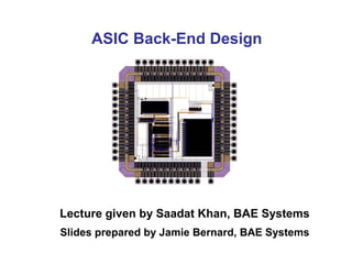
- 1. ASIC Back-End Design Lecture given by Saadat Khan, BAE Systems Slides prepared by Jamie Bernard, BAE Systems
- 2. Agenda • Introduction • Design Flow – Overview – Floorplan – Timing Driven Placement – Clock Tree Synthesis – Routing • Verification • Design Example
- 4. Introduction • Technological Advances – 19th Century - Steel – 20th Century – Silicon • Growth in Microelectronic (Silicon) Technology – Moore’s Law (# of transistors double/18 months) – One Transistor – Small Scale Integration (SSI) • Multiple Devices (Transistor / Resistor / Diodes) • Possibility to create more than one logic gate (Inverter, etc) – Large Scale Integration (LSI) • Systems with at least 1000 logic gates (Several thousand transistors) – Very Large Scale Integration • Millions to hundreds of millions of transistors (Microprocessors) – Intel indicates that dual core processors will soon exist that contain 1 billion transistors
- 5. Introduction • Manual (Human) design can occur with small number of transistors • As number of transistors increase through SSI and VLSI, the amount of evaluation and decision making would become overwhelming (Trade-offs) – Maintaining performance requirements (Power / Speed / Area) – Design and implementation times become impractical • How does one create a complex electronic design consisting of millions of transistors? Automate the Process using Computer-Aided Design (CAD) ToolsAutomate the Process using Computer-Aided Design (CAD) Tools
- 6. Introduction • CAD tools provide several advantages – Ability to evaluate complex conditions in which solving one problem creates other problems – Use analytical methods to assess the cost of a decision – Use synthesis methods to help provide a solution – Allows the process of proposing and analyzing solutions to occur at the same time • Electronic Design Automation – Using CAD tools to create complex electronic designs (ECAD) – Several companies who specialize in EDA • Cadence® Design Systems • Magma® Design Automation Inc. • Synopsys® CAD Tools Allow Large Problems to be SolvedCAD Tools Allow Large Problems to be Solved
- 8. Design Flow - Overview • Generic VLSI Design Flow from System Specification to Fabrication and Testing • Steps prior to Circuit/Physical design are part of the FRONT-END flow • Physical Level Design is part of the BACK- END flow – Physical Design is also known as “Place and Route” • CAD tools are involved in all stages of VLSI design flow – Different tools can be used at different stages due to EDA common data formats* • Synopsys® CAD tool for Physical Design is called Astro™
- 9. What does Astro™ do?
- 10. Where does the Gate Level Netlist come from? 1st Input to Astro™
- 11. Standard Cell Library 2nd Input to Astro™ • Pre-designed collection of logic functions – OR, AND, XOR, etc • Contains both Layout and Abstract views – Layout (CEL) contains drawn mask layers required for fabrication – Abstract (FRAM) contains only minimal data needed for Astro™ – Timing information • Cell Delay / Pin Capacitance • Common height for placement purposes
- 12. • Integrated circuits are built out of active and passive components, also called devices: – Active devices • Transistors • Diodes – Passive devices • Resistors • Capacitors • Devices are connected together with polysilicon or metal interconnect: – Interconnect can add unwanted or parasitic capacitance, resistance and inductance effects • Device types and sizes are process or technology specific: – The focus here is on CMOS technology Basic Devices and Interconnect 38
- 13. Transistor or Device Representation Gates are made up of active devices or transistors.Gates are made up of active devices or transistors. CMOS Inverter Example OUTIN Gate Schematic IN OUT PMOS NMOS Transistor or Device View VDD GND 37
- 14. What is “Physical Layout”? Physical Layout – Topography of devices and interconnects, made up of polygons that represent different layers of material. CMOS Inverter Example NMOS PMOS OUT VDD GND Physical or Layout View ININ OUT PMOS NMOS Transistor or Device View VDD GND 39
- 15. Layout or Mask (aerial) view Silicon Substrate Process of Device Fabrication • Devices are fabricated vertically on a silicon substrate wafer by layering different materials in specific locations and shapes on top of each other • Each of many process masks defines the shapes and locations of a specific layer of material (diffusion, polysilicon, metal, contact, etc) • Mask shapes, derived from the layout view, are transformed to silicon via photolithographic and chemical processes Wafer (cross-sectional) view 40
- 16. Wafer Representation of Layout Polygons Example of complimentary devices in 0.25 um CMOS technology or process. Input VDD GND Output PMOS NMOS 0.25 um Aerial or Layout View Wafer Cross-sectional View 41
- 17. Contacts: Connecting Metal 1 to Poly/Diff’n Diffusion, Poly and Metal layers are separated by insulating oxide. Connecting from Poly or Diffusion to Metal 1 requires a contact or cut. Cut or Contact (a hole in the oxide) VDD IN GND Diffusion Diffusion Poly Oxide insulation Metal 1 Metal 1 49
- 18. What is meant by “0.xx um Technology”? - In CMOS Technology the um or nm dimension refers to the channel length, a minimum dimension which is fixed for most devices in the same library. - Current flow or drive strength of the device is proportional to W/L; Device size or area is proportional to W x L. Gate or Channel Dimensions (L and W) Narrow er Width = Lower current throug h channe l Length Widt h G A T E W L L Width (W) Wider Width = Higher current throug h channe l G A T E Length 42
- 19. Comparing Technologies The drive strength of both devices is the same: W/L = 6. The diffusion area (5xLxW) of A is 4x that of B. A: 0.5 um Technology L = 0.5 um 2L 2L W = 3 um L = 0.25 um W = 1.5 um 2L 2L B: 0.25 um Technology Area Comparison 43
- 20. Relative Device Drive Strengths To double the drive strength of a device, double the channel width (W), or connect two 1X devices in parallel. The latter approach keeps the height at a fixed or “standard” height. “1X” NMOS (W/L = 6) GND OUT L = 0.25 um W = 1.5 um IN 0.25 um GND 3 um OUT IN “2X” NMOS (W/L = 12) 1.5 um GND 0.25 um OUT IN “2X” NMOS (W/L = 6 + 6) 44
- 21. Input Output Gate Drive Strength Example PMOS transistor 1x NMOS transistor Input Output Parallel PMOS transistors 2x inv1 inv2 Parallel NMOS transistors Each gate in the library is represented by multiple cells with different drive strengths for effective speed vs. area optimization. 45
- 22. Drive/Buffering Rules: Max Transition/Cap 1x 2x 1x 1x 1x Maximum Transition Rule Violation Maximum Transition Rule Met Upsized Driver or Added Buffers AfterOptimization BeforeOptimization 46
- 23. Timing Constraints 3rd Input to Astro™ • Derived from system specifications and implementation of design • Identical to timing constraints used during logic synthesis • Common constraints in electronic designs – Clock Speed/Frequency – Input / Output Delays associated with I/O signals – Multicycle Paths – False Paths • Astro™ uses these constraints to consider timing during each stage of the place and route process
- 24. Concept of Place and Route • Location of all standard cells is automatically chosen by the tool during placement (Based upon routing and timing) • Pins are physically connected during routing (Based upon timing)
- 25. Concepts of Placement • Standard cells are placed in “placement rows” • Cells in a timing-critical path are placed close together to reduce routing related delays (Timing Driven) • Placement rows can be abutting or non-abutting
- 26. Concepts of Routing • Connecting between metal layers requires one or more “vias” • Metal Layers have preferred routing directions – Metal 1 (Blue) Horizontal – Metal 2 (Yellow) Vertical – Metal 3 (Red) Horizontal
- 28. Design Flow – Floorplan • Layout design done at the chip level – Defining layout hierarchy – Estimation of required design area • A blueprint showing the placement of major components in the design (non-standard cell) – Inputs / Output (I/O) – RAMs / ROMs/ – Reusable Intellectual Property (IP) macros • Approaches to Floorplanning (Automatic or Manual) – Constructive – Iterative – Knowledge-Based
- 29. Design Must Be Floorplanned Before P&R • Floorplan of design: – Core area defined with large macros placed – Periphery area defined with I/O macros placed – Power and Ground Grid (Rings and Straps) established • Utilization: – The percentage of the core that is used by placed standard cells and macros – Goal of 100%, typically 80-85%
- 30. I/O Placement and Chip Package Requirements • Some Bond Wire requirements: – No Crossing – Minimum Spacing – Maximum Angle – Maximum Length
- 31. Guidelines for a Good Floorplan • A few quick iterations of place and route with timing checks may reveal the need for a different floorplan
- 32. Defining the Power/Ground Grid and Blockages • Purpose of Grid is to take the VDD and VSS received from the I/O area and distribute it over the core area • Blockages can also be added in the floorplan to prohibit standards cells from being placed in those areas
- 33. Timing Driven PlacementTiming Driven Placement
- 34. Design Flow – Timing Driven Placement • Astro™ optimizes, places, and routes the logic gates to meet all timing constraints • Balancing design requirements – Timing – Area – Power – Signal Integrity
- 35. Timing Constraints • Astro™ needs constraints to understand the timing intentions – Arrival time of inputs – Required arrival time at outputs – Clock period • Constraints come from the Logic Synthesis tool – SDC (Synopsys Design Constraints) format
- 36. Cell and Net Delays • Astro™ calculates delay for every cell and every net • To calculate delays, Astro™ needs to know the resistance and capacitance of each net – Uses geometry of net and Look Up Tables to estimate the resistances and capacitances
- 37. Timing Driven Placement • Timing Driven Placement places critical path cells close together to reduce net RC • Prior to routing, RC are based on Virtual Routes • What if critical paths do not meet timing constraints with placement?
- 38. Logic Optimizations • These optimizations can be done during pre-place, in-place, or post-place stages of placement • Each optimization can be done separately or all done concurrently during placement (none – one – all)
- 39. Clock Tree SynthesisClock Tree Synthesis
- 40. Design Flow – Clock Tree Synthesis • All clock pins are driven by a single clock source • Large delay and transition time due to length of net • Clock signal reach some registers before others (Skew)
- 41. Clock Tree Topologies • Clock source is connected to center of the network • Networks are distributed in a H or X shape until clock pin of register is driven by a local buffer H-Tree and X-Tree Topologies Solve Single Clock Pin ProblemH-Tree and X-Tree Topologies Solve Single Clock Pin Problem
- 42. After Clock Tree Synthesis • A clock (buffer) tree is built to balance the output loads and minimize the clock skew • A delay line can be added to the network to meet the minimum insertion delay (clock balancing)
- 43. Gated - CTS • Clocks may not be generated directly from I/O • Power saving techniques such as clock-gating are used to turn of the clock to sections of the design • Astro™ can interpret gated clocks and can build clock trees “through” the logic to the registers
- 44. Effects of CTS • Several (Hundreds/Thousands) of clock buffers added to the design • Placement / Routing congestion may increase • Non-clock cells may have been moved to less ideal locations • Timing violations can be introduced
- 45. RoutingRouting
- 46. Process of Routing Can Be Timing DrivenProcess of Routing Can Be Timing Driven Design Flow – Routing • Routing is a fundamental step in the place and route process • Create metal shapes that meet the requirements of a fabrication process – The physical connection between cells in the design • Virtual routes used during placement and CTS need to become reality – Timing of design needs to be preserved – Timing data such as signal transitions and clock skew needs to match the virtual route estimates
- 47. Timing Driven Routing • Routing along the timing-critical path is given priority – Creates shorter, faster connections • Non-critical paths are routed around critical areas – Reduces routing congestion problems for critical paths – Does not adversely impact timing of non-critical paths
- 48. Concept of Routing Tracks • Metal routes must meet minimum width and spacing “design rules” to prevent open and short circuits during fabrication • In grid based routing systems, these design rules determine the minimum center-to-center distance for each metal layer (Track/Grid spacing) • Congestion occurs if there are more wires to be routed than available tracks
- 49. Grid-Based Routing System • Metal traces (routes) are built along and centered around routing tracks • Each metal layer has its own tracks and preferred routing direction – Metal 1 – Horizontal – Metal 2 – Vertical • Track and pitch information can be located in the technology file – Design Rules
- 51. What Happens After Place and Route? Verification
- 52. Formal Verification • New standard cells have been added to the design through timing optimizations and clock tree synthesis • The final netlist created by Astro™ needs to be compared to the original gate-level netlist • Formal verification ensures the functional equivalency at the logic level between the two implementations (original vs. final) of the design – The intended function was maintained throughout the physical design process Formality® is the Sign-Off Tool for Formal VerificationFormality® is the Sign-Off Tool for Formal Verification
- 53. Timing Verification • Star-RCXT™ performs the layout parasitic extraction of the resistances and capacitances of all routes in the design • Results in a format such as SPEF (Standard Parasitic Extended Format) – SPEF is an smaller, extended format of Standard Parasitic Format (SPF), which enables the transfer of design specific resistances and capacitances from physical design to timing analysis and simulation tools • Primetime® performs static timing analysis – Detects timing violations by combining SPEF from Star-RCXT™ and netlist from Astro™ and checks against the design timing constraints (clock frequencies) Star-RCXT™ and Primetime® are the Sign-Off Tools for Timing Verification Star-RCXT™ and Primetime® are the Sign-Off Tools for Timing Verification
- 54. Physical Verification • Checks the design for fabrication feasibility and physical defects that could result in the design to not function properly – 3 checks (DRC, ERC, and LVS) • Design Rule Checks (DRC) – Verifies that design does not violate any fabrication rules associated with the target process technology (metal width/space, antenna ratio, etc) • Electrical Rules Checks (ERC) – Verifies that there are no short or open circuits with power and ground as well as resistors/capacitors/transistors with floating nodes (part of LVS) • Layout Versus Schematic (LVS) – Final physical design matches the logical (schematic) version in terms of correct connectivity and number of electrical devices Hercules™ is the Sign-Off Tool for Physical VerificationHercules™ is the Sign-Off Tool for Physical Verification
- 55. Fabrication • Physical Design process is complete upon successful completion of timing, functional, and physical verification • The design can be “Taped-Out” and GDSII created for the manufacturer – GDSII (Graphic Design System II) is a binary format containing the physical geometry information of the design. – The shapes are assigned numeric attributes in the form of “Layer Number” and “Data Type” (Metal 1 => 100:0) • Fabrication and Test determine which chips can be implemented into the system (yield)
- 56. Physical design Data GDSII (Stream) Masks Wafer Mask Generation – GDSII / Stream 30
- 57. Example Design – Cory Ellinger Independent Study • 64x8 FIFO Block. – Inputs: • Direct input • Input through 64-bit addition • Read, Write, Enable, and Sum Control – Able to be read and written simultaneously – Outputs: • 64-bit FIFO out • Overflow flag • Full, Empty flags
- 58. Block Diagram register register unsignedAdder register bank clk rst add_fifo sum_cnt 64 x 8 FIFO rd wr en full empty overfl 6464 64 64 data_in_x data_in_y_fifo_in data_out
- 59. Block Diagram – Critical Path register register unsignedAdder register bank clk rst add_fifo sum_cnt 64 x 8 FIFO rd wr en full empty overfl 6464 64 64 data_in_x data_in_y_fifo_in data_out Critical Path
- 60. Major Physical Design Steps • Floorplan • Placement • Clock Tree Synthesis • Routing
- 61. Floorplanning • Aspect Ratio • Power Planning • Utilization • Pin Placement • Macro Placement • Define Core Rows and Routing Tracks • Read in Netlist, Libraries, and SDC. • Groups and Regions
- 62. Floorplan (Theoretical) Aspect Ratio (2:1) W:H FIFO Input Register Data Flow 64 data_in data out output flags 64 data_in sum_cnt clk reset
- 63. Floorplan
- 64. Floorplan Showing Logic Modules
- 65. Placement • Timing Driven Standard Cell Placement • Ignore Scan Chains ( if any ) • Timing – First look at non-wire load model timing. – Concentrate on any large setup violations. – Ignore violations caused by design rule failures.
- 66. AutoPlace of Logic Modules
- 67. Design Placement
- 68. Reset Net
- 70. Clock Tree Synthesis • Goals: – Low Clock Skew – Low Clock Insertion Delay – Sharp Transitions • Timing – Setup violations clean – Design Rules fixed – Initial evaluation of real hold violations
- 71. Post Clock Tree Synthesis
- 72. Routed Design
- 73. Route (zoom)
Editor's Notes
- <number>
- <number>
- <number>
- <number>
- <number>
- <number>
- <number>
- <number>
- <number>
- <number>
- <number> Fabrication Processes (also called Technologies) are built for specific target applications, which require different types of devices. Here are some technology examples and their application(s): Bipolar:Analog design. High Power CMOS:Digital design; Low power BiCMOS:(Bipolar and CMOS) Mixed Analog/Digital or Bipolar high-drive outputs of CMOS designs DRAM:Memories EEPROM:Reprogamable circuits GaAs:RF (Radio Frequency) designs The process assumed in this course is CMOS (Complementary Metal Oxyde Semiconductor), widely used for digital designs: -High performance (integration density and speed) -Low power -Low manufacturing costs (fewer masks)
- <number> The basic building component of a gate is a FET (Field Effect Transistor). CMOS (Complimentary Metal Oxide Semiconductor FET) uses two types of FETs: P-type and N-type. A CMOS Inverter, the most basic CMOS gate, consists of one P-FET and its complimentary N-FET. The input terminals of complimentary transistors are wired together with a Polysilicon strap (also called the input “gate”) and likewise the output terminals are connected with a Metal strap. Most other gates consist of multiple pairs of P- and N-FETs. A 2-input NAND gate is made up of 2 pairs of transistors, or 4 transistors. A 2-input NAND gate is usually the “reference unit” when describing the size of other gates or design sizes. For example an INVERTER is the equivalent of 0.5 gates; an OR gate is the equivalent of 1.5 gates; a Flip Flop could be 4-8 gates. Reference to a design size of 500k Gates, for example, usually refers to 500k “equivalent 2-input NAND Gates”, or 2 Million transistors. Basic operation of an inverter: If a ZERO voltage (Logic “0”) is applied to the Input or Gate terminal (Poly), then the P-Channel FET is turned ON and the N-Channel FET is turned OFF. The output terminal is now connected to VDD and the path to ground is disconnected. The output terminal is pulled and held high to VDD (Logic “1”). When a voltage of VDD (Logic “1”) is applied to the Input or Gate terminal (Poly), then the P-Channel FET is turned OFF and the N-Channel FET is turned ON. The output terminal is now connected to GND and the path to VDD is disconnected. The output terminal is pulled and held low to GND (Logic “0”).
- <number> Semiconductor devices are built or fabricated by growing, implanting and depositing materials on a silicon wafer. Polygons of a specific color or layer represent an aerial view of the specific areas on the silicon wafer where a particular material, represented by that layer, will be implanted or deposited. The composite picture of all of these layers superimposed on each other is called the layout or physical view of the design. Before the devices can be fabricated, each polygon layer is converted into one or more masks (see next page). How devices are formed: In the inverter example above, the dark green solid rectangle at the bottom represents an N-type Diffusion Area, while the pea-green stipple-patterned rectangle above represents P-type Diffusion, inside of a pink N-Well area. A transistor device is formed when a conductive material called polysilicon (poly for short), the stippled red line, crosses over and splits the diffusion area into two regions. The poly over the diffusion becomes the gate of both the N- and PMOS devices, and the two separated diffusion regions per device are called the source and drain regions. The source is usually connected to power or ground and the drain usually forms the device output or connects to another device’s source. The blue striped lines represent Metal 1, either aluminum or copper, which acts as interconnect. The small solid black squares are contacts or cuts, which form electrical connections between metal and diffusion or poly.
- <number> A mask is a glass plate with shapes represented by either opaque or clear areas (depending on if the process step requires a positive or negative image). A photolithographic process allows light to pass through the clear areas of the mask onto the silicon wafer, which is covered by photo-sensitive material. Through chemical processes either the exposed or non-exposed areas will be etched away, depending again on the step, thereby exposing only key underlying areas. These areas are then either ion-implanted (forming “diffusion” areas) or covered with material (metal, polysilicon, oxide insulation) through a deposition step. The fabrication process entails processing the silicon wafer through numerous chemical and photo-lithographical steps, using multiple masks, to build up all the required layers of materials which create the required devices. The next page shows a cross-sectional view of a basic N- and PMOS device.
- <number> CMOS technology implies that all active devices, or transistors, come in pairs of N- and PMOS transistors. On the left side, you see the layout implementation of the N- and PMOS devices. Each material layer (poly, metal1, diffusion, etc) is represented in layout tools by polygons of a unique color and layer number. When a design is “taped-out”, this refers to the process of writing out each mask layer in the a format called GDSII. The GDSII file is then used to create the individual glass masks for each process layer. On the right side, you see the same devices fabricated on silicon. The masks, which were derived from the 2-dimensional layout representation of the devices, were used to fabricate 3-dimensional devices in silicon. The reference made to the “0.25 um technology”, refers to the minimum width of the polysilicon gate, the red striped polygon above, which this particular process can build (see next page).
- <number> A contact is literally a hole in the oxide insulation layer through which the metal can “droop” down and touch the poly or diffusion surface, creating an electrical connection between the two layers. A contact is the connector between Metal 1 and the layers below, polysilicon or diffusion. The connector between metal layers is called a “via”. (See next page)
- <number> This course discusses primarily CMOS technology. In the drawing above, solid green = diffusion and striped red = polysilicon (poly). MOS transistors are formed where poly overlaps diffusion. The area where poly and diffusion intersect forms the “gate”, which controls the current flow (on/off) from one side of the diffusion, across the “channel”, to the other side of the diffusion. The gate dimensions determine the transistor’s area (proportional to W x L) and strength (proportional to W/L): the Width (W) is a diffusion dimension (channel width) and the Length (L) is the poly dimension (channel length). The ratio W/L is proportional to the amount of current the FET can deliver, or its “Drive strength” (the ability to charge/discharge capacitive load). For a given channel length L, the larger the width of the transistor the greater the drive capacity. It follows that the pull-up or pull-down speed of a transistor improves as the width is increased. Example: a 4um/0.25um device has twice the drive strength, or current flow, as a 2um/0.25um device. L is the minimum dimension which a particular process is able to manufacture and is the same for most transistors on the same chip. A “0.13um technology” means L = 0.13um. The size requirements of the transistors for each logic function are determined by performing timing analysis (static or dynamic) to determine the delays of all logic paths. If the delay of a particular path does not meet the design’s timing constraints, gates (devices) along the critical path can be up-sized to achieve faster speeds. The penalty for faster devices (upsizing) is a corresponding increase in silicon area needed to implement the faster gates. Balancing speed vs area is a common challenge in CMOS technology.
- <number> The 3/0.5 device on the left has the same drive strength as the middle 1.5/0.25 device but the latter takes up ¼ of the area. You could theoretically fit four 0.25um devices in the area that one 0.5um device of identical strength takes up (right picture), therefore the push to continually reduce the channel L or minimum technology size. (Note: the length of the diffusion, the dimension perpendicular to the channel width, is usually 1 or 2 times the minimum technology dimension L. In this case the device size, which is essentially the diffusion area, is directly proportional to W x L.)
- <number> In a standard cell library each logic gate is usually implemented with multiple drive capabilities. Example: a 2-input NAND gate might have 1X (nand2_1), 2X (nand2_2), 4X (nand2_4) etc versions. This enables synthesis and layout tools to choose the right size gate to achieve the desired speed constraints, while minimizing the area of the design. Besides having a fixed channel length L for all devices, what makes a standard cell “standard” is that the cell height is fixed or standardized, so that cells can be placed next to each other in rows with standard heights. To achieve this devices are “strengthened” by placing two or more minimum-size devices in parallel (rightmost picture) instead of making the diffusion of one device wider (middle picture).
- <number> During synthesis and layout phases the design tools choose the smallest cell with enough drive level to satisfy the timing and drive/buffering requirements of the given circuit.
- <number> In addition to meeting timing, the output of every gate usually has one or more “drive rules”, which must also be met. Example: maximum capacitance, maximum transition and/or maximum fanout rules. These rules or constraints help to reduce transient power consumption and ensure that gate loads stay within the characterized range of the delay models, among other things. If a maximum transition constraint is violated (example above), this can be handled by increasing the drive strength of the gate or by buffering the load on the net sufficiently to reduce the transition slope. The dotted waveform on the left represents the minimum transition “drive” or “buffering rule”, which is being violated as shown by solid waveform. On the right the transition time meets the minimum transition rule after buffer optimization. If a maximum capacitance constraint is violated upsizing the driver may not fix the problem if the max capacitance rule of the upsized driver is the same as the smaller one (since upsizing does not affect the capacitive loading). In this case only buffering the load helps.
- <number>
- <number>
- <number>
- <number>
- <number>
- <number>
- <number>
- <number>
- <number>
- <number>
- <number>
- <number>
- <number>
- <number>
- <number>
- <number>
- <number>
- <number>
- <number>
- <number>
- <number>
- <number>
- <number>
- <number>
- <number>
- <number>
- <number>
- <number>
- <number>
- <number>
- <number>
- <number>
- <number>
- <number> GDS II is the industry-standard data format for physical designs. The format was developed at Calma, once the industry leader in CAD systems. Because GDS II was used by so many companies as new tools were developed, the GDS II format became the default format. The GDS II format is used to make physical designs portable between different systems and different data bases. GDS II is a polygon-based format; it does not understand multi-level components such as transistor elements.
- <number>
- <number>
- <number>
- <number>
- <number>
- <number>
- <number>
- <number>
- <number>
- <number>
- <number>
- <number>
- <number>
- <number>
- <number>
- <number>
- <number>
- <number>