This paper presents an educational kit (simulation & practical electronic circuit) for a PWM inverter, which can be used to educate Electronics Engineering undergraduate students the structure and behavior of a PWM’s inverter pulse generator. This module is taught as part of the “Power Electronics” course of the Department of Electronics Engineering of Piraeus University of Applied Sciences. The concept is to offer our co-students the opportunity to deeply understand how the pulse generator of the inverter works, by virtually and practically experimenting with the pulse generator itself creating the necessary models in the popular platform of MULTISIM (Simulation Tool of National Instruments) and designing/constructing the respective PCB circuits in the also popular platform of ULTIBOARD (Circuit Design Tool of National Instruments). This is important for the success of the learning process of this course. Though it is accompanied with a real-world laboratory, this exercise has not been yet added in the course’s laboratory curriculum.
simulation and implementation of a spwm inverter pulse for educational purposesEleftheriosSamiotis1
This paper aims to develop and implement an educational kit for a Sinusoidal Pulse Width Modulation (SPWM) inverter pulse generator circuit, which can be used to educate Electronics Engineering undergraduate students the structure and behavior of a SPWM’s inverter pulse generator. The developed electronic circuit is simulated and implemented using low cost and reliable electronic parts. The concept is to offer under/postgraduate students the opportunity to deeply understand how a SPWM pulse generator works, by virtually and practically experimenting with the pulse generator itself creating the necessary models in the popular platform of MULTISIM (Simulation Tool of National Instruments) and designing/constructing the respective PCB circuits in the also popular platform of ULTIBOARD (Circuit Design Tool of National Instruments). This work is also useful for engineers who deal with operation and maintenance (O&M) of inverters, because it provides a deeper knowledge and understanding of all operational characteristics of every stage of the SPWM electronic pulse generator of an inverter
This document summarizes a research paper on fuzzy control of a multicell converter. It begins with an introduction to stacked multicell converters, which allow sharing of voltage and current stresses across switches. It then discusses the topology and operation of the multicell converter. Sinusoidal pulse width modulation is used to control the output voltage. Fuzzy logic control is then proposed to control the RMS voltage value using MATLAB. Simulation results show that total harmonic distortion is reduced with increasing voltage levels in the multicell converter output waveform. Open and closed loop control of a 6x2 multicell converter are analyzed through MATLAB simulation.
In this paper the multicarrier pulse width modulation (MCPWM) with multi value DC voltage source multilevel inverter is presented. These MLI’s are suitable in high voltage & high power application due to their ability to synthesize waveforms with better harmonic spectrum. Seven level inverter is simulated using MATLAB/Simulink. The use of Photovoltaic Cell as a DC source for the multilevel Inverter is proposed here.
Harmonic Minimization In Multilevel Inverters By Using PSOIDES Editor
Harmonic Elimination in a multilevel inverters is
an optimization problem which is solved by applying particle
swarm optimization (PSO) technique. The derived equation
for the computation of total harmonic distortion (THD) of the
output voltage of the multilevel inverter is used as the objective
function in PSO algorithm. The objective function used is to
reduce the THD of the multilevel inverter and obtain the
corresponding switching angles with the elimination of
possible lower order harmonics. In this paper a pseudo code
based algorithm is proposed to deal with inequality constraints
which will helps in accelerating the optimization process. The
proposed method is applied for seven level cascade inverter to
eliminate the 5th and 7th order harmonics to reduce the total
harmonic distortion .This proposed PSO algorithm is effective
in reducing the total harmonic distortion corresponding the
range of modulation index. The simulation results shows that
the proposed PSO method is indeed capable of obtaining
higher quality of solutions to eliminate 5th and 7th order
harmonics and to reduce the total harmonic distortion of 7-
level cascade inverter
Performance Evaluation of Nine Level Modified CHB Multilevel Inverter for Var...IJMER
International Journal of Modern Engineering Research (IJMER) is Peer reviewed, online Journal. It serves as an international archival forum of scholarly research related to engineering and science education.
Multilevel DC Link Inverter with Reduced Switches and BatteriesIJPEDS-IAES
Multilevel inverters are the best solution for medium and high voltage power electronic drives. Because of its unique characteristic of synthesizing sinusoidal voltage with less harmonic contents using several DC sources. In a three phase multilevel inverter, each phase of a cascaded H-bridge inverter requires ‘n’ DC sources to obtain 2n + 1 output voltage levels. One particular disadvantage is that, it increases number of power semiconductor switches. To overcome this disadvantage a multilevel DC link inverter (MLDCLI) with reduced number of switches and batteries is proposed.
IRJET- Mitigation of Harmonics in Active Neutral Point Clamped Multilevel Inv...IRJET Journal
This document presents a simulation of a 7-level active neutral point clamped (ANPC) inverter. It begins with an introduction to multilevel inverters and discusses issues with conventional 5-level NPC and flying capacitor topologies. It then presents the objectives to develop a Simulink model of a 7-level ANPC inverter using MATLAB. The model is described including subsystems for the source, pulse generation, and switches. Simulation results showing the output voltage and current waveforms are presented, with THD values below 13% for voltage and 6% for current.
This document provides an overview of operational amplifiers (op-amps) including:
1. It introduces op-amps and describes their ideal characteristics of infinite gain, infinite input impedance, and zero output impedance.
2. It discusses practical op-amp parameters and specifications including gain, input bias currents, input offset, power supply effects, and more.
3. It describes common op-amp circuits like inverting amplifiers, non-inverting amplifiers, summing amplifiers, integrators, and differentiators and explains their operations and applications.
Comparison of thd reduction for asymmetrical cascaded h bridge invertereSAT Publishing House
IJRET : International Journal of Research in Engineering and Technology is an international peer reviewed, online journal published by eSAT Publishing House for the enhancement of research in various disciplines of Engineering and Technology. The aim and scope of the journal is to provide an academic medium and an important reference for the advancement and dissemination of research results that support high-level learning, teaching and research in the fields of Engineering and Technology. We bring together Scientists, Academician, Field Engineers, Scholars and Students of related fields of Engineering and Technology
Analysis of Multilevel Inverter using Bipolar and Unipolar Switching Schemes ...ijsrd.com
Cascaded H-bridge Multilevel Inverter (MLI) is most efficient topology for medium and high voltage DC-AC conversion, having less output harmonics and less commutation losses. Disadvantages are their complexity, more number of power devices, passive components and a complex control circuitry. Here a Cascaded Hybrid Multilevel Inverter is used to produce a three phase 9-level output voltages. Now a day inverter is also know as a DC-AC converter, is one of the most popular part of electrical device. This proposed inverter widely used in industries application such as speed control of induction motor. This thesis focus on three phase 9-level bipolar and unipolar switching inverter with characteristics like output voltage boosting ability and also we discus about the bipolar and unipolar switching scheme along with capacitor voltage control. The modified topology uses Cascaded H-bridge (CHB) with bidirectional and unidirectional switches producing boost up output voltage. Here a hybrid Pulse Width Modulation (PWM) technique is applied to control the power devices. This modulation technique uses a sine wave and a repeating wave, these waves are combined and a complete reference wave is generated. There is comparative study between CHB and modified topology between number of power devices used and Total Harmonic Distortions (THD). THD of modified topology is reduced and analyzed by FFT window. The results are observed by MATLAB/SIMULINK software.
SIMULATION ANALYSIS OF CLOSED LOOP DUAL INDUCTOR CURRENT-FED PUSH-PULL CONVER...Journal For Research
The current electronic devices require DC power source, which is taken from a battery or DC power supply. DC-DC converter is utilized to get regulated dc voltage from unregulated one. Switched mode power supply (SMPS) are commonly used in industrial applications, because of more advantages compared to linear power supply. In SMPS we have isolated and non-isolated converters, where isolated converters are frequently used, in order to get more voltage with multiple outputs. So among different isolated converters, push-pull converter is chosen for micro converter applications to obtain high voltage conversion ratio by using HF transformer, due to their better utilization of transformer. New methodology of control is implemented for making ZVS and ZCS at same time and to reduce the number of switches in the secondary side of dual inductor CFPP converter, which is a voltage doubler circuit. This becomes the solution for problem identification. Thus this converter with soft-switching reduces the switching losses.The current-fed push-pull converters are used in many applications like photo-voltaic (PV) power converters for boosting the output voltage. Push-pull converter is chosen for micro converter applications, to obtain high voltage conversion ratio by using high frequency (HF) transformer, due to their better utilization of transformer. This deals with the design of dual inductor CFPP converter, where zero voltage switching (ZVS) and zero current switching (ZCS) is achieved for the primary side of the converter by using secondary switches. Primary side switches are controlled by closed loop control topology. The secondary side is made with voltage doubler to obtain high voltage. Open loop and closed loop control of dual inductor current fed push pull converter simulation is finished by MATLAB/SIMULINK and their outcomes are analyzed.
Efficient Power Factor Correction For Multipulse Bridgeless Active Boost Conv...IRJET Journal
This document presents a modified power factor correction boost converter with a bridgeless active boost converter for a three-phase AC-DC converter system. The proposed design improves upon a conventional 24-pulse rectifier by using a bridgeless topology where the inductor current flows through only two semiconductor devices rather than three. Simulation results show that the proposed bridgeless boost 24-pulse converter improves the power factor from 0.715 to 0.982 compared to the conventional 24-pulse rectifier design.
The document contains a list of 134 topics related to power electronics and drives. The topics cover various fields including renewable energy, multilevel converters, resonant converters, Z-source inverters, industrial drive control applications for traction systems and aircraft, and more. The list provides a short description for each topic and indicates the corresponding research field.
A review of pfc boost converters for hybrid electric vehicle battery chargersiaemedu
1) The document reviews different types of PFC boost converters that can be used for Plug-in Hybrid Electric Vehicle (PHEV) battery chargers, including conventional, bridgeless, interleaved, and bridgeless interleaved topologies.
2) The conventional boost converter is well-suited for power levels up to 1 kW due to diode bridge losses and heat dissipation issues at higher power. The bridgeless topology avoids the rectifier bridge but has EMI and voltage sensing challenges.
3) Interleaved and bridgeless interleaved topologies offer improvements like lower ripple current and higher effective switching frequency, making them suitable for power levels up to 3 kW and 5 kW, respectively.
This document discusses cascaded H-bridge multilevel inverters and their symmetrical and asymmetrical configurations. It begins by introducing two-level and multilevel inverters, noting that multilevel inverters are better suited for high power and voltage applications as they reduce harmonics. There are three main multilevel inverter topologies: neutral-point-clamped, flying capacitors, and cascaded H-bridges. The cascaded H-bridge topology connects H-bridge cells in series to generate stepped voltage waveforms. Symmetrical configurations use equal DC voltages for each cell, while asymmetrical configurations use unequal voltages, allowing more voltage levels with the same number of cells. The document presents simulations of
This document presents a simulation study of a photovoltaic (PV) system that uses a cascade three-level inverter topology. The PV system consists of a PV array, boost converter, and inverter. A cascade three-level inverter is formed by connecting two two-level inverters in series. Space vector PWM control is used to generate switching pulses. MATLAB/Simulink studies are performed to analyze the total harmonic distortion in the output voltage and current waveforms when supplying an inductive load. The simulation results demonstrate the operation of the proposed PV system with the cascade three-level inverter.
A New Multilevel Inverter Structure For High-Power Applications using Multi-c...IJPEDS-IAES
This document presents a new multilevel inverter structure that can be used in high-power applications. The proposed topology uses a cascaded connection of basic units, each consisting of a full-bridge inverter. This reduces the number of required components compared to other multilevel inverter structures. Two methods are presented for determining the DC voltage source values: a symmetric method where all sources have the same value, and an asymmetric method where the values differ. A multi-carrier PWM strategy is used to generate the switching signals. Simulation results show the 25-level inverter generates output voltages and currents with total harmonic distortions of 5.57% and 0.083%, respectively.
A seven level cascaded multilevel dstatcom for compensation of reactive power...IAEME Publication
This document describes a seven-level cascaded multilevel DSTATCOM system for compensating reactive power and harmonics. It uses a cascaded H-bridge multilevel inverter with either phase shifted PWM or level shifted PWM modulation techniques. Simulation results show the system is able to compensate load current harmonics and reactive power, reducing the total harmonic distortion of source currents from 36.89% to 4.37% with a seven-level inverter using phase shifted PWM. The DSTATCOM provides unity power factor correction at the point of common coupling.
ACADEMIC MATLAB SIMULATION 2013/14/15 PROJECTS FOR
• ELECTRICAL AND ELECTRONICs ENGINEERING[EEE]
• POWER ELECTRONICs AND DRIVES[PED]
• POWER SYSTEMS[PS]….
We Can also Develop Your Own Ideas and Your IEEE Papers With Extension also…
We also write papers for your projects and give guidance for paper publishing.
For Further Details Call Us @
0-9347143789/9949240245
Visit us at: www.asokatechnologies.in
For Abstracts of IEEE papers and For Any Queries
Mail us : asokatechnologies@gmail.com
This document summarizes a lab experiment on designing and testing an open-loop boost converter circuit. Key details include:
- The purpose is to design, simulate, and test an open-loop boost converter to boost 12V DC input to 20V DC output.
- Simulation and hardware tests were conducted at half-load to analyze the inductor current, switch voltage, and switch current waveforms.
- The waveforms matched between simulation and hardware tests, validating the open-loop boost converter design meets specifications.
Performance and Analysis of Hybrid Multilevel Inverter fed Induction Motor Drivernvsubbarao koppineni
This paper presents the Five level inverter with single DC source which is used to generate a five level output with two bridges and six switches and performance of three phase induction motor is analyzed when connected to PV array For this two identical dc sources of 50V each for two bridges in five levels using Multi level inverter and five level output is obtained by using a single DC source of 100V with six switches. A virtual DC source (charged capacitor acts as virtual DC source) is used for getting the output. The same technique is implemented for three-phase circuit i.e. by using single DC source. An asynchronous motor (three-phase) is connected as load and its performance characteristics are analyzed. And further the DC source is replaced by a renewable resource such as solar panels, fuel cell etc. and DC voltage is obtained. Performance characteristics of three-phase asynchronous motor are analyzed with PV array connected. The method can be easily extended to an m-level inverter.
Simulation and study of multilevel inverter (report)Arpit Kurel
The document discusses the simulation and study of a multilevel inverter. It begins with an abstract that outlines that multilevel inverters are used to convert DC power to AC power at required voltage and frequency levels for applications like motor drives and grid connections. It then discusses different multilevel inverter topologies like diode clamped, flying capacitor, and cascaded H-bridge. For this project, a three phase five level inverter is simulated using sinusoidal PWM technique in MATLAB/Simulink. The topology used is a cascaded H-bridge inverter with separate DC sources. The multilevel inverter reduces harmonic contents in the output waveform compared to a three level inverter.
APPLICATIONS OF FLOATING-GATE MOSFET IN THE DESIGN OF INVERTER AND RING OSCIL...elelijjournal
This paper presents the application of floating-gate MOSFET (FGMOS) in the design of low voltage and
high speed digital circuits wherein threshold voltage tunability of FGMOS has been exploited to enhance
the performance of inverter in terms of various parameters like switching threshold voltage, noise margins,
propagation delay and energy delay product. It has been observed that by varying the bias voltage in
FGMOS, the voltage transfer characteristics can be altered that result in lowering of switching threshold
voltage, increased noise margins, reduced propagation delay and less energy delay product as compared to
the standard CMOS inverter. This paper also demonstrates the design of ring oscillator using FGMOS and
it has been found that FGMOS based ring oscillator exhibits higher frequency of oscillation as compared to
its CMOS counterpart. The performance of these circuits has been verified through PSpice simulations
carried out using level 7 parameters in 0.13 µm CMOS technology with a supply voltage of 1 V.
SIMULATION AND STUDY OF MULTILEVEL INVERTER (ppt)Arpit Kurel
This document discusses the simulation and study of a multilevel inverter. It aims to simulate a three-phase five-level inverter using MATLAB/Simulink. Multilevel inverters are attractive for medium-voltage high-power applications as they can produce outputs with low distortion at medium voltages. The document reviews literature on multilevel inverters and various topologies. It then discusses objectives of simulating a five-level inverter to reduce harmonics. Simulation results show that a five-level inverter has lower total harmonic distortion and higher efficiency compared to a three-level inverter.
Stand alone regulated single phase five level inverter with coupled inductorIAEME Publication
This document summarizes a research paper presented at the International Conference on Emerging Trends in Engineering and Management in 2014. The paper proposes a stand-alone regulated single phase five level inverter with a coupled inductor. It includes a high step-up DC-DC converter as a front-end stage to stabilize the output voltage from a variable DC source. The converter uses a coupled inductor to attain high voltage gain. The inverter can produce a five level AC output without variation in amplitude. The operation of the DC-DC converter and inverter are explained. Simulation and experimental results demonstrate the circuit can provide a constant output voltage waveform from different DC input voltages.
Simulation of Five Level Diode Clamped Multilevel Inverterrahulmonikasharma
The power electronics device which converts DC power to AC power at required output voltage and frequency level is known as inverter. The voltage source inverters produce an output voltage or a current with levels either 0 or +ve or-ve V dc. They are known as two-level inverters. Multilevel inverter is to synthesize a near sinusoidal voltage from several levels of dc voltages. Multilevel inverter has advantage like minimum harmonic distortion. Multi-level inverters are emerging as the new breed of power converter options for high power applications. They typically synthesize the stair-case voltage waveform (from several dc sources) which has reduced harmonic content. Multi-level inverters have many attractive features, high voltage capability, reduced common mode voltages near sinusoidal outputs, low dv/dt, and smaller or even no output filter; sometimes no transformer is required at the input side, called the transformer-less solution, making them suitable for high power applications In this paper a 5-level Diode clamped multilevel inverter is developed by IGBTS using Simulink. Gating signals for these IGBTS have been generated by designing comparators. In order to maintain the different voltage levels at appropriate intervals, the conduction time intervals of IGBT have been maintained by controlling the pulse width of gating pulses[6] (by varying the reference signals magnitude of the comparator). The simulation results for 5-level and THD for the output have been identified by MATLAB/SIMULINK.
SINGLE PHASE SYMMETRICAL MULTILEVEL INVERTER DESIGN FOR VARIOUS LOADSelelijjournal
This paper presents a single phase symmetrical multilevel inverter with various loads. This proposed
topology is connected with R-load, RL-load and induction motor drive with unipolar Phase disposition
PWM technique. Among the four modulation technique it gives reduced harmonic. This proposed topology
has less number of switches than the conventional one. In conventional cascaded multilevel inverter have
twelve switches and the proposed topology have eight switches. Totally the four switches have been
reduced from the conventional one. It is designed to produce a seven level output. The simulation analysis
has been done by a MATLAB/SIMULINK model.
Comprehensive Study of Single-Phase AC-DC Power Factor Corrected Converters w...Asoka Technologies
Solid-state switch mode AC-DC converters having high-frequency transformer isolation are developed in buck, boost, and buck-boost configurations with improved power quality in terms of reduced total harmonic distortion (THD) of input current, power-factor correction (PFC) at AC mains and precisely regulated and isolated DC output voltage feeding to loads from few Watts to several kW. This paper presents a comprehensive study on state of art of power factor corrected single-phase AC-DC converters configurations, control strategies, selection of components and design considerations, performance evaluation, power quality considerations, selection criteria and potential applications, latest trends, and future developments. Simulation results as well as comparative performance are presented and discussed for most of the proposed topologies.
Electrical Discharge Machining Flyback Converter using UC3842 Current Mode PW...IJPEDS-IAES
This paper presents a current mode Pulse Width Modulation (PWM) controlled Flyback converter using UC3842 for Electrical Discharge Machining current generator control circuit. Circuit simplicity and high efficiency can be achieved by a Flyback converter with current mode PWM controller. The behaviors of the system's operation is analyzed and discussed by varying the load resistance. Matlab sofware is used to simulate the Flyback converter where a prototype has been built and tested to verify its performance.
Analysis of a Quasi Resonant Switch Mode Power Supply for Low Voltage Applica...IDES Editor
QRC provides efficient and regulated switch mode
power supplies for robotic and satellite applications. This paper
addresses the enhanced controller techniques for high
frequency isolation based push-pull Quasi Resonant
Converter. This technique is similar to the conventional PI
controller technique but varies only the enhancement
constants to improve the time domain response of the
converter. The proposed converter is designed for low output
voltage and power rating, characteristically 5V and 5 W, with
the comprehension of current design trends towards enhanced
performance. At the primary stage, to validate the design of
the converter, simulation is performed in PSIM for ±50% load
variations. A prototype model of this converter is developed.
The results obtained from the experimental set-up are
presented and analysed in detail. The results reveal the
superiority of the proposed method.
International Journal of Engineering Research and DevelopmentIJERD Editor
The document proposes a new multi-string inverter topology for photovoltaic systems connected to the electric grid. It connects multiple PV strings in parallel through diodes before boosting the DC voltage and converting it to AC with an inverter. Simulations show the multi-string topology offers higher efficiency compared to traditional string inverters by reducing losses.
Design and Simulation of Efficient DC-DC Converter Topology for a Solar PV Mo...Sajin Ismail
Modulated Integrated Converter systems are considered to be the new and global turning point in the field of
Solar PV systems. These converters are highly recognised for its modular size and compact nature and they are supposed to
be attached directly with each PV module and since one PV module is having the power rating of a few watts ranging from
0-500Ws, the design rating would be in the same range and thus the most vital condition in such a design is efficiency
under these relatively low loads. In this paper an isolated interleaved boost converter topology is considered in the DC-DC
section and which is designed and simulated for a specific power rating (250W) and the efficiency is analysed with varying
load conditions and compared with the target efficiency of the system.
Modified Bidirectional Converter with Current Fed InverterIJPEDS-IAES
A bidirectional dc-dc converter with multiple outputs are concatenated with a
high frequency current source parallel resonant push pull inverter is
presented in this paper. The two outputs are added together and it is taken as
the input source for the inverter. The current source parallel resonant push
pull inverter implemented here with high frequency applications like
induction heating, Fluorescent lighting, Digital signal processing sonar. This
paper proposes a simple photovoltaic power system consists of a
bidirectional converter and a current fed inverter for regulating the load
variations. Solar power is used as the input source for the system. Simulation
of the proposed system is carried out in PSIM software and experimentally
verified the results.
Real Time Implementation of Variable Step Size Based P&O MPPT for PV Systems ...IJPEDS-IAES
Nowadays Solar energy is an important energy source due to the energy crisis and environment pollution. Maximum power point tracking (MPPT) algorithm improves the utilization efficiency of a photovoltaic systems. In this paper an improved P&O MPPT algorithm is developed and simulated using MATLAB / SIMULINK to control the DC/DC buck converter. The obtained simulink model is also verified using dspace tool. Both the simulated and experimental results are validated by also comparing them with conventional MPPT methods. The performance measures show the increase in the efficiency of PV system by the proposed model.
Hardware Implementation of Solar Based Boost to SEPIC Converter Fed Nine Leve...IJPEDS-IAES
Multi level inverters are widely used in high power applications because of
low harmonic distortion. This paper deals with the simulation
and implementation of PV based boost to SEPIC converter with multilevel
inverter. The output of PV system is stepped up using boost to sepic
converter and it is converted into AC using a multilevel inverter.
The simulation and experimental results with the R load is presented in this
paper. The FFT analysis is done and the THD values are compared. Boost to
SEPIC converter is proposed to step up the voltage to the required value. The
experimental results are compared with the simulation results. The results
indicate that nine level inverter system has better performance than seven
level inverter system.
This document summarizes a student project report on analyzing a flyback converter. The project involved designing a simulation circuit for a flyback converter with an input of 12V DC and output of 240V DC. The report includes chapters on the operating principle, simulation, results, and conclusions. The key findings were that the flyback converter was able to step up the input voltage to the desired output level, and the output voltage, current, and input voltage waveforms were obtained through simulation as desired. The switching element used was a MOSFET due to its high power rating and switching speed.
This paper introduces a new topology of multilevel inverter, which is able to operate at high performance. This proposed circuit achieves requirements of reduced number of switches, gate-drive circuits, and high design flexibility. In most cases fifteen-level inverters need at least twelve switches. The proposed topology has only ten switches. The inverter has a quasi-sine output voltage, which is formed by level generator and polarity changer to produce the desired voltage and current waveforms. The detailed operation of the proposed inverter is explained. The theoretical analysis and design procedure are given. Simulation results are presented to confirm the analytical approach of the proposed circuit. A 15-level and 31-level multilevel inverters were designed and tested at 50 Hz.
project report on plc based load sharingVivek Arun
This document provides information about the hardware requirements for a PLC based load sharing project. It discusses transformers, diodes, PLCs, rectifiers, resistors, capacitors, relays, LEDs, and DC motors. Transformers are used to convert AC voltages and connect multiple power sources in parallel. Diodes allow current to flow in one direction. PLCs are used for automation and control. Rectifiers convert AC to DC. Resistors and capacitors are basic electronic components. Relays, LEDs, and DC motors are also used in the circuit. The project aims to automatically share loads between multiple transformers connected to the system based on the load level.
This document summarizes a study that simulated a grid-connected photovoltaic (PV) system incorporating an efficient maximum power point tracking (MPPT) algorithm. The study used PSIM software to model the PV module, boost converter with Perturb and Observe MPPT control, and inverter connecting the PV array to the grid. Simulation results showed the model achieved the MPPT function and improved the inverter output by reducing voltage ripple.
International Journal of Engineering Research and Applications (IJERA) is an open access online peer reviewed international journal that publishes research and review articles in the fields of Computer Science, Neural Networks, Electrical Engineering, Software Engineering, Information Technology, Mechanical Engineering, Chemical Engineering, Plastic Engineering, Food Technology, Textile Engineering, Nano Technology & science, Power Electronics, Electronics & Communication Engineering, Computational mathematics, Image processing, Civil Engineering, Structural Engineering, Environmental Engineering, VLSI Testing & Low Power VLSI Design etc.
Filter Based Solar Power Generation System with a Seven Level InverterIJMTST Journal
This paper proposes a new solar power generation system, which is composed of a DC/DC power converter and a new seven-level inverter. The DC/DC power converter integrates a DC-DC boost converter and a transformer to convert the output voltage of the solar cell array into two independent voltage sources with multiple relationships. This new seven-level inverter is configured using a capacitor selection circuit and a full-bridge power converter, connected in cascade. The capacitor selection circuit converts the two output voltage sources of DC-DC power converter into a three-level DC voltage and the full- bridge power converter further converts this three- level DC voltage into a seven-level AC voltage. In this way, the proposed solar power generation system generates a sinusoidal output current that is in phase with the utility voltage and is fed into the utility. The salient features of the proposed seven-level inverter are that only six power electronic switches are used and only one power electronic switch is switched at high frequency at any time. A prototype is developed and tested to verify the performance of this proposed solar power generation system.
Modeling Of Converter “Single Phase to Three Phase by Using Single Phase Sup...IJMER
This document discusses modeling a converter to generate three-phase power from a single-phase source. It proposes a model that uses a bridge rectifier to convert the single-phase AC supply to DC, and then a three-arm IGBT inverter to convert the DC back to three-phase AC. The model is simulated in MATLAB Simulink. The simulation results show the transformer primary and secondary voltages and currents, inverter pulses and currents, and the phase currents and voltages generated. The proposed converter model can generate three-phase power for small industries, large buildings, and workshops from a single-phase supply.
This document presents a simulation study of a novel three-phase AC-AC converter that uses space vector pulse width modulation (SVPWM) at the rectifier and inverter stages. The converter employs unity power factor control to maintain a unity power factor between the input voltage and current. Six cases of simulations were run with varying output voltages, frequencies, and loads. The results show the converter is able to maintain a stable DC link voltage of 1000V while producing sinusoidal output voltages with varying amplitudes and frequencies. The input current is also sinusoidal and in phase with the voltage, demonstrating a unity power factor is achieved across all simulation cases.
This simulation summarizes a student's bachelor's thesis on solid state transformers using cascaded H-bridge converters. It describes a proposed 20kVA cascaded H-bridge converter based solid state transformer connecting to a 12kV distribution system. Key components include a cascaded AC/DC rectifier, dual active bridge converters with high frequency transformers, and a DC/AC inverter. The simulation models this design in NI Multisim, using IGBT switches and various control circuits to regulate the voltage and power flow between the primary and secondary sides. Simulation results demonstrate voltage regulation through phase control of the rectifiers and output voltage control of the SPWM inverters.
IRJET- Design and Implementation of Converters using MPPT in an Eco VehicleIRJET Journal
1) The document describes the design and implementation of converters using maximum power point tracking (MPPT) in a solar electric vehicle. A SEPIC converter is used to regulate the nonlinear output from the photovoltaic panels and MPPT with perturb and observe algorithm is used to track maximum power.
2) Fuzzy logic control is applied to control the SEPIC converter. The obtained voltage from the photovoltaic system is stored in a 48V battery. This improves the overall efficiency and performance of the solar electric vehicle.
3) The SEPIC converter regulates the fluctuating DC output from the solar panels into a stiff DC output. Fuzzy logic control provides pulse width modulated signals to the SEPIC converter to control
This document compares buck and boost converter topologies for use in photovoltaic power systems to maximize power extraction from solar panels. It finds that the boost converter is better suited as the PV interface as it can maintain continuous input current flow to the load. Simulation results show that a boost converter tracking the maximum power point of a PV array can increase the output voltage from 17.1V to 24.9V and deliver 60W of power to the load. The boost converter also performs well under varying temperature and solar irradiation conditions according to the simulations.
This document proposes an efficient solar powered induction motor drive system for water pumping applications. It uses a photovoltaic array, push-pull DC-DC boost converter, and three-phase inverter with the solar array as the energy source. Two PWM techniques, sinusoidal PWM and space vector PWM, are implemented and compared for the inverter switching. Incremental conductance algorithm is used for maximum power point tracking of the PV array. Simulation results in MATLAB/SIMULINK are presented to verify the effectiveness of the proposed design.
This document discusses control techniques for three-phase PWM rectifiers. It presents three main control techniques: 1) Hysteresis-band PWM control which uses a hysteresis current controller; 2) Carrier-based sinusoidal PWM control which uses a triangular carrier wave; 3) Voltage oriented control with hysteresis-band PWM which is a vector control technique. MATLAB simulations of each technique are presented and their performance is compared based on total harmonic distortion and power factor. Hysteresis control and voltage-oriented control achieve near unity power factor but with THD over 5%, while carrier-based PWM control achieves less than 5% THD.
Similar to educational pwm inverter pulse generator (20)
DEEP LEARNING FOR SMART GRID INTRUSION DETECTION: A HYBRID CNN-LSTM-BASED MODELgerogepatton
As digital technology becomes more deeply embedded in power systems, protecting the communication
networks of Smart Grids (SG) has emerged as a critical concern. Distributed Network Protocol 3 (DNP3)
represents a multi-tiered application layer protocol extensively utilized in Supervisory Control and Data
Acquisition (SCADA)-based smart grids to facilitate real-time data gathering and control functionalities.
Robust Intrusion Detection Systems (IDS) are necessary for early threat detection and mitigation because
of the interconnection of these networks, which makes them vulnerable to a variety of cyberattacks. To
solve this issue, this paper develops a hybrid Deep Learning (DL) model specifically designed for intrusion
detection in smart grids. The proposed approach is a combination of the Convolutional Neural Network
(CNN) and the Long-Short-Term Memory algorithms (LSTM). We employed a recent intrusion detection
dataset (DNP3), which focuses on unauthorized commands and Denial of Service (DoS) cyberattacks, to
train and test our model. The results of our experiments show that our CNN-LSTM method is much better
at finding smart grid intrusions than other deep learning algorithms used for classification. In addition,
our proposed approach improves accuracy, precision, recall, and F1 score, achieving a high detection
accuracy rate of 99.50%.
Electric vehicle and photovoltaic advanced roles in enhancing the financial p...IJECEIAES
Climate change's impact on the planet forced the United Nations and governments to promote green energies and electric transportation. The deployments of photovoltaic (PV) and electric vehicle (EV) systems gained stronger momentum due to their numerous advantages over fossil fuel types. The advantages go beyond sustainability to reach financial support and stability. The work in this paper introduces the hybrid system between PV and EV to support industrial and commercial plants. This paper covers the theoretical framework of the proposed hybrid system including the required equation to complete the cost analysis when PV and EV are present. In addition, the proposed design diagram which sets the priorities and requirements of the system is presented. The proposed approach allows setup to advance their power stability, especially during power outages. The presented information supports researchers and plant owners to complete the necessary analysis while promoting the deployment of clean energy. The result of a case study that represents a dairy milk farmer supports the theoretical works and highlights its advanced benefits to existing plants. The short return on investment of the proposed approach supports the paper's novelty approach for the sustainable electrical system. In addition, the proposed system allows for an isolated power setup without the need for a transmission line which enhances the safety of the electrical network
Understanding Inductive Bias in Machine LearningSUTEJAS
This presentation explores the concept of inductive bias in machine learning. It explains how algorithms come with built-in assumptions and preferences that guide the learning process. You'll learn about the different types of inductive bias and how they can impact the performance and generalizability of machine learning models.
The presentation also covers the positive and negative aspects of inductive bias, along with strategies for mitigating potential drawbacks. We'll explore examples of how bias manifests in algorithms like neural networks and decision trees.
By understanding inductive bias, you can gain valuable insights into how machine learning models work and make informed decisions when building and deploying them.
Using recycled concrete aggregates (RCA) for pavements is crucial to achieving sustainability. Implementing RCA for new pavement can minimize carbon footprint, conserve natural resources, reduce harmful emissions, and lower life cycle costs. Compared to natural aggregate (NA), RCA pavement has fewer comprehensive studies and sustainability assessments.
Embedded machine learning-based road conditions and driving behavior monitoringIJECEIAES
Car accident rates have increased in recent years, resulting in losses in human lives, properties, and other financial costs. An embedded machine learning-based system is developed to address this critical issue. The system can monitor road conditions, detect driving patterns, and identify aggressive driving behaviors. The system is based on neural networks trained on a comprehensive dataset of driving events, driving styles, and road conditions. The system effectively detects potential risks and helps mitigate the frequency and impact of accidents. The primary goal is to ensure the safety of drivers and vehicles. Collecting data involved gathering information on three key road events: normal street and normal drive, speed bumps, circular yellow speed bumps, and three aggressive driving actions: sudden start, sudden stop, and sudden entry. The gathered data is processed and analyzed using a machine learning system designed for limited power and memory devices. The developed system resulted in 91.9% accuracy, 93.6% precision, and 92% recall. The achieved inference time on an Arduino Nano 33 BLE Sense with a 32-bit CPU running at 64 MHz is 34 ms and requires 2.6 kB peak RAM and 139.9 kB program flash memory, making it suitable for resource-constrained embedded systems.
International Conference on NLP, Artificial Intelligence, Machine Learning an...gerogepatton
International Conference on NLP, Artificial Intelligence, Machine Learning and Applications (NLAIM 2024) offers a premier global platform for exchanging insights and findings in the theory, methodology, and applications of NLP, Artificial Intelligence, Machine Learning, and their applications. The conference seeks substantial contributions across all key domains of NLP, Artificial Intelligence, Machine Learning, and their practical applications, aiming to foster both theoretical advancements and real-world implementations. With a focus on facilitating collaboration between researchers and practitioners from academia and industry, the conference serves as a nexus for sharing the latest developments in the field.
A review on techniques and modelling methodologies used for checking electrom...nooriasukmaningtyas
The proper function of the integrated circuit (IC) in an inhibiting electromagnetic environment has always been a serious concern throughout the decades of revolution in the world of electronics, from disjunct devices to today’s integrated circuit technology, where billions of transistors are combined on a single chip. The automotive industry and smart vehicles in particular, are confronting design issues such as being prone to electromagnetic interference (EMI). Electronic control devices calculate incorrect outputs because of EMI and sensors give misleading values which can prove fatal in case of automotives. In this paper, the authors have non exhaustively tried to review research work concerned with the investigation of EMI in ICs and prediction of this EMI using various modelling methodologies and measurement setups.
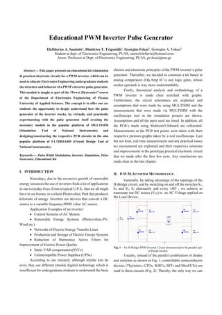
1.
Abstract — This paper presents an educational kit (simulation
& practical electronic circuit) for a PWM inverter, which can be
used to educate Electronics Engineering undergraduate students
the structure and behavior of a PWM’s inverter pulse generator.
This module is taught as part of the “Power Electronics” course
of the Department of Electronics Engineering of Piraeus
University of Applied Sciences. The concept is to offer our co-
students the opportunity to deeply understand how the pulse
generator of the inverter works, by virtually and practically
experimenting with the pulse generator itself creating the
necessary models in the popular platform of MULTISIM
(Simulation Tool of National Instruments) and
designing/constructing the respective PCB circuits in the also
popular platform of ULTIBOARD (Circuit Design Tool of
National Instruments).
Keywords — Pulse Width Modulation, Inverter, Simulation, Pulse
Generator, Educational Kit
I. INTRODUCTION
Nowadays, due to the excessive growth of renewable
energy resources the use of inverters finds a lot of applications
in our everyday lives. From a typical U.P.S., that we all might
have in our homes, to a whole Photovoltaic Park that produces
kilowatts of energy. Inverters are devices that convert a DC
source to a variable frequency/RMS value AC source.
Application Examples of an inverter:
Control Systems of AC Motors
Renewable Energy Systems (Photovoltaic-PV,
Wind etc.)
Networks of Electric Energy Transfer Lines
Production and Storage of Electric Energy Systems
Reduction of Harmonics Active Filters for
Improvement of Electric Power Quality
Static VAR compensators(SVCs)
Uninterruptible Power Supplies (UPSs)
According to our research, although similar kits do
exist, they use different (mainly digital) technology which is
insufficient for undergraduate students to understand the basic
electric and electronic principles of the PWM inverter’s pulse
generator. Thereafter, we decided to construct a kit based in
analog comparators (Op-Amp IC’s) and logic gates, whose
modus operandi is way more understandable.
Firstly, theoretical analysis and methodology of a
PWM inverter is made clear enriched with graphs.
Furthermore, the circuit schematics are explained and
assumptions that were made by using MULTISIM and the
measurements that were made via MULTISIM with the
oscilloscope tool in the simulation process are shown.
Assumptions and all the parts used are listed. In addition, all
the PCB’s made using Multisim/Ultiboard are collocated.
Measurements at the PCB test points were taken with their
respective pictures-graphs taken by a real oscilloscope. Last
but not least, real time measurements and any practical issues
we encountered are explained and their respective solutions
and improvements in the prototype practical electronic circuit
that we made after the first few tests. Any conclusions are
made clear in the last chapter.
II. P.W.M. INVERTER METHODOLOGY.
Generally, by taking advantage of the topology of the
H-Bridge circuit, and by switching on and off the switches S1,
S4 and S2, S3 alternately and every 180o
, we achieve to
transmute our DC source (VIN) to an AC Voltage applied on
the Load Device.
Fig. 1 – An H-Bridge PWM Inverter Circuit demonstrated with parallel pair
of Diode-Switch.
Usually, instead of the parallel combination of diodes
and switches as shown in Fig. 1, controllable semiconductor
devices (Thyristors, GTOs, IGBTs, BJTs and MosFETs) are
used in these circuits (Fig. 2). Thereby, the only way we can
Educational PWM Inverter Pulse Generator
Eleftherios A. Samiotis1
, Dimitrios T. Trigonidis1
, Georgios Fokas1
, Georgios A. Vokas2
Student at dept. of Electronics Engineering, PUAS, samiotislefteris@hotmail.com
Assoc. Professor at Dept. of Electronics Engineering, PUAS, gvokas@puas,gr
2. interact with these circuits is by controlling when and whereas
the semiconductor devices are going to be activated or not.
This can be achieved by low power circuits called Pulse
Generators.
Fig. 2 – An H-Bridge PWM Inverter Circuit demonstrated with parallel pair
of Diode – Semiconductor Device (MosFETs).
A PWM Inverter is a device, as we already mentioned,
that converts a DC Voltage to a variable frequency or/and
variable RMS Voltage AC source like an invert air
conditioner where the 230V/50Hz of the electric power
network is converted to a DC Voltage by a high wattage
Power Supply and then this DC voltage gets inverted to a
variable frequency (not 50Hz) and variable RMS Voltage AC
(not 230V). A PWM inverter can be used to supply with
energy mostly ohmic and capacitive loads or devices while
for inductive loads or devices a similar device with a little bit
of different specs called SPWM Inverter is used. A PWM
inverter cannot be used to supply an inductive load as the
pulse that produces consists of infinite harmonics and so, the
THD factor is massive (over 100%) causing destructive
effects to the load/device. The connection of the load or the
device at the output of the inverter (LOAD R_L_C) is shown
to Fig. 2. The conversion by an H-Bridge PWM Power
Inverter of a DC to an AC Voltage is shown in Fig. 3.
Fig.. 3 – DC to AC Conversion by a PWM H-Bridge Inverter.
III. P.W.M. REAL IMPLEMENTATION (PCBS) AND
SIMULATION (USING NI’S ULTIBOARD & MULTISIM).
P.W.M. Generator Simulation (NI’s Multisim).
A. Assumptions for NI’s Multisim and design and
program results at the Test Points.
To begin with, our pulse generator is line
communicating, which means that it doesn’t have a built in
generator in order to generate the Sinus wave it uses for
comparison, but it uses a relegated sample from the Electric
Power Network with the help of a relegation (230V to 15V)
transformer. This also means that the working frequency of
the Inverter is locked at 50Hz like the frequency of the electric
power network. The entire philosophy of this pulse generator
for the P.W.M Power inverter is based into two simple
comparisons with the AC sample.
In order to make the necessary comparisons two
variable DC sources are needed. One positive, and one
negative. Changing the value of the DC source, the width of
the produced pulse changes too, and by modulating the pulse
width we achieve to affect the RMS voltage that the
load/device will consume. For instance, we can achieve full
(100%) power on an AC light bulb when the lighting
conditions are poor and we can also demand half the power or
less (<50%) when the lighting conditions are better where less
artificial light is required. The circuit that used both for
simulation and the PCBs is shown in Fig. 4.
Fig. 4 – PWM Circuit designed in Multisim.
Firstly, we compare the AC sample (red) with the
positive DC (orange) source, producing a series of Pulses
(blue) as shown in Fig. 5.
3. Fig. 5 – AC and High Positive DC Voltage Comparison and Output Pulse.
The output pulses of this comparator can much wider
if the positive DC Voltage is dropped near 0 Volts (Fig. 6).
Fig. 6 - AC and Near 0V Positive DC Voltage Comparison and Output Pulse.
Also, the same AC sample (red) is compared with the
negative DC source (orange), producing another series of
pulses (blue) as shown in Fig. 7.
Fig. 7 – AC and Negative DC Voltage Comparison and Output Pulse.
The output pulses of this comparator can much wider
if the negative DC Voltage is dropped near 0 Volts (Fig. 8).
Fig. 8-AC and near 0V Neg. DC Voltage Comparison and Output Pulse.
Both (Fig. 5) and (Fig. 7) Pulses (blue) end to the 1st
2-input AND logic gate. The Pulse (blue) produced in the
output of the gate (Fig. 9) is used to trigger the S1, S4
MosFETs (Fig. 2). Various output pulses can occur if the
length of the input pulses at AND1/2 gates change (Fig. 10).
Fig. 9 – AND1 Gate Inputs and Output.
Fig. 10 – A Variation on the AND1/2 output pulses when the compared DC
voltage changes.
Simultaneously, pulses from the comparators also end
to a NOT logic gate, producing pulses that they are inverted
versions from the previous pulses.
4. Both of those inverted pulses end to a 2nd 2-input
AND logic gate. The pulse produced in the output of the gate
(Fig. 11) is used to trigger the S2, S3 MosFETS (Fig. 2).
Fig. 11 – AND2 inputs and output.
The output pulses that will get to all S1, S4 (red) and
S2, S3 (blue) of the pulse generator for the P.W.M. Power
Inverter are shown in the next Fig. (Fig. 12).
Fig. 12 – Outputs to the power inverter S1, S4 (red) and S2, S3 (blue)
Also, if the compared DC voltage changes the total
output of the pulse generator of the inverter changes, as shown
in the next Fig.s (Fig. 13, 14).
Fig.s 13, 14 – Various Output levels of the inverter.
That is the case when different power output in
needed. Fig. 14 is when the inverter works at 100% power and
Fig.s 13 is when the output of the inverter is less.
B. P.W.M. Real Implementation Technique
Assumptions and Parts Used
Due to the availability of our university, instead of
comparator chips, we used operational amplifiers (Op-Amps)
without input and feedback resistors so they can work as
comparators. The op-amps used were two TI’s LF411 IC’s.
An AND gate chip (74LS08) and a NOT gate chip
(74LS04) were used for the logic functions.
For the power supply several parts and regulators were
used. Firstly, a 2x18 V/3 A transformer is used to reduce the
AC voltage from the Electric Power Network, then a full
bridge rectifier(PB1010) is used to rectify the voltage, and
some filter capacitors are used too(Electrolytic of Various
Values at 35V). After this, to supply the logic gates an
LM7805 voltage regulator is used.
For the positive variable voltage an LM317 regulator
IC was used. For the negative variable voltage a LM337
regulator IC is used, and this part of the power supply was
added afterwards. So, instead of making a new PCB we
created a smaller one to be connected with the main power
supply. Last but not least, to supply the op-amps a set of
LM78/7915 ICs are used.
Design of the PCB of the PWM Pulse Generator Circuit.
Using NI’s Multisim and Ultiboard, the circuits and
the printed board circuits were designed. The PCBs were
finally carved with a CNC Router at PUAS Electronics
Engineering Department with the help of our
technician/professor. The designs can be shown in the
pictures below, starting with the Power Supply Main
Multisim Circuit shown in Fig. 15.
5. Fig. 15 – Power Supply circuit by MS.
The Power Supply Main PCB is presented in Fig. 16.
Fig. 16 – Power Supply PCB by Ultiboard.
The Power Supply PS337 (secondary) Multisim Circuit is
presented in Fig. 17.
Fig. 17 – Secondary PS Circuit by MS.
The Power Supply (secondary) PS337 PCB is presented in
Fig. 18.
Fig. 18 – Secondary PS PCB by Ultiboard.
The Pulse Generator Multisim Circuit is presented in Fig. 19
Fig. 19 – Pulse Generator Circuit by Multisim.
The Pulse Generator PCB is presented in Fig. 20.
Fig. 20 – Pulse Generator PCB by Ultiboard.
The Final Boards after the Assembling and Soldering are
presented in Figs 21, 22.
6. Fig.s 21, 22 – The PCBs after the assembling and soldering.
Graphs from oscilloscope at the test points
After assembling and soldering the PCB certain tests
were made to be sure that the circuit works as it should work.
The only electronic measuring instrument used, was an
Agilent Technologies DSO1024A quad channel/200 MHz
oscilloscope.
In the picture below (Fig. 23), the pulses for the S1, S4
MosFETs (Yellow Color) and the pulses for the S2, S3
MosFETs (Green Color) can be shown.
Fig.s 23 – Output pulses at the TPs during the test runs in our Dept.
(Electronics) at University (PUAS).
IV. RESULTS AND DISCUSSION
A. P.W.M. Issues
The most important issue of a PWM is that it cannot
supply an inductive load, but only resistive or capacitive loads
and a combination of them.
Another issue is that in this generator the frequency of
the AC sample cannot be controlled and so the frequency of
the Output AC is locked to this of the electric power network
(50Hz/20ms), as it is line commutating.
Also, both the positive and the negative DC source at
the same time with a stereo potentiometer cannot be
controlled, because the two regulators respond differently to
the input. So, instead of one stereo potentiometer, two mono
potentiometers were used.
Finally, despite the fact that in the simulation perfect
pulses can be seen, into the oscilloscope several spikes due to
noise can be detected. The noise probably occurs due to the
fact that the parts that have been used are not of high grade
(space, military, etc.), they are of commercial grade, and they
are subside to environment conditions (PCB rust, humidity
temperature etc.) and probably have some defects from
production.
B. Improvements/Suggestions
After experimenting with the generator, several
improvements came up to the table making the generator
smaller, more efficient with lower cost of construction. More
specifically:
During the Design: In Multisim/Theoretical Design
Power Supply as presented in the following Fig. 24.
Fig. 24 – The circuit of the improved PS.
During the stage of PCB Power Supply as presented in
the following Fig. 25.
Fig. 25 – The PCB of the improved PS.
7. During the Multisim/Theoretical Design of PWM
stage, as presented in Fig. 26.
Fig. 26 – The Circuit of the improved PWM pulse generator.
Concerning the PCB PWM stage, as presented in Fig. 27.
Fig. 27 – The PCB of the improved PWM pulse generator.
First of all, we realized that using 15 volts to supply
the op-amps is useless when they can be supplied by the same
5 volts as the logic gates.
Also, the sample AC is now suppressed at 5 volts peak,
therefore only a 2x5V, 3A transformer (way cheaper than the
one previously used) is now needed.
In addition, instead of the variable regulators
LM317/LM337 classic regulators LM7905/LM7805 with a
potentiometer were used.
After all these modifications the power supply was
simplified. Also, we observed that under 5 volts power
supply, the circuit works more efficiently.
Regarding to the PWM itself a stereo potentiometer for
both regulators can now be used to control the comparisons.
Taking the above into account, the output of the
improved circuit as simulated in Multisim is presented in the
following Figs 28 and 29.
Fig. 28 – Output pulses (pink – S1, S4), (L. blue – S2, S3) of the improved
PWM generator with high negative (blue) and positive DC voltage (green)
compared with the AC (red) of the network
Fig. 29 – Output pulses (pink – S1, S4), (L. blue – S2, S3) of the improved
PWM generator with high negative (blue) and positive DC voltage (green)
compared with the AC (red) of the network.
V. CONCLUSIONS
A PWM inverter is amongst the most useful devices in
the world of power electronics. The aim of this paper was to
provide an educational PWM design and implementation
procedure as well as the corresponding power part of a dc/ac
inverter. The major parts of this procedure were presented,
while improvements in design and hardware elements are
proposed. The students can observe every part of the pulse
generating procedure in both simulation and real circuit. As
future work, an SPWM pulse generator is to be designed and
implemented in the existing power part of the inverter having
the possibility to verify the capability of the inverter to
eliminate the harmonic components as designed.
REFERENCES
Microelectronic Circuits 6th Edition, Adel S. Sedra, Kenneth C.
Smith, 2016.
Power Electronics: Circuits, Devices & Applications 1st Edition,
Muhamad H. Rashid, 2015.
Power Electronics 4st edition, Stefanos Manias, 2016.
http://www.ti.com
http://www.st.com
http://www.ni.com
NI Multisim: Circuit Design Suite Pro 12.0.
NI Ultiboard: Circuit Design Suite Pro 12.0.