Downloaded 788 times


![2 CHAPTE R 1 BASI C CONCEPTS
1.1
System of Units
Figure 1,1 •••~
Standard 51 prefixes,
1.2
Basic Quantities
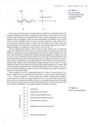
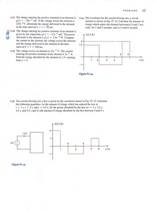
I, = 2 A
@
(al
12 = - 3 A
~(bl
. ..:..Figure 1,2 l
Conventional current flow:
(a) positive current flow;
(b) negative current flow.
The system of units we employ is the international system of units, the Syslcme international
des Unites, which is normally referred to as the SI standard system. This system, which is
composed of the basic units meter (m), kilogram (kg), second (s), ampere (A), kelvin (K),
and candela (cd), is defined in all modern physics texts and therefore will not be defined here,
However, we will discuss the units in some detail as we encounter them in our subsequent
analyses.
The standard prefixes that are employed in SI are shown in Fig. 1.1. Note the decimal rela-
tionshi p between these prefi xes. These standard prefi xes are employed throughout O llf slUdy
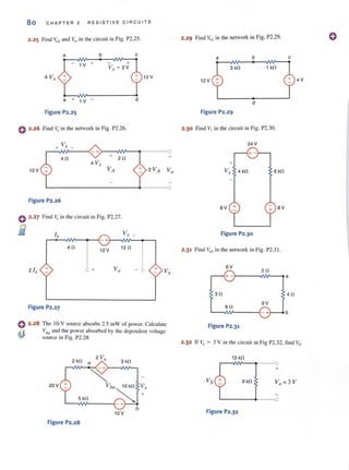
of electric circuits.
Circuillcchnoiogy has changed drastically over the years. For example, in the early 1960s
the space on a circuit board occupied by the base of a single vacuum tube was about the size
of a quaner (25-cel11 coin). Today that same space could be occupied by an Intel Penlium
integrated circuit chip containing 50 million transistors. These chi ps are the engine for a host
of electron ic equipment.
10- 12 10-9 10-6 10- 3 10' 10' 10' 1012
I I I I I I I I
pico (pI nano (n) micro (II.) milli (m) kilo (kl mega (MI giga (GI lera (TI
Before we begin our analysis of electric circuits, we must define terms that we will employ.
However, in th is chapter and throughout the book our definitions and explanations will be as
simple as possible to foster an understanding of the use of the material. No attempt will be
made to give complete definitions of many of the quantities because such defi nitions are not
only unnecessary at this level but are often confusing. Although 1110st of us have an intuitive
concept of what is meant by <l circuit. we will simply refer to an elee1ric circlli1 as an inter-
connection of electrical components, each of which we will describe with a mathematical
model.
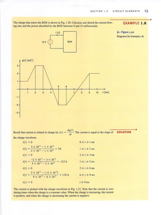
The most elementary quantity in an analysis of electric circuits is the electric charge. Our
interest in electric charge is centered around its motion, since charge in motion results in an
energy transfer. Of p<1I1icular interest to us are those situations in which the motion is confined
to a definite closed path.
An e lectric c ircuit is essentiall y a pipeline that facilitates the transfer of charge from
one point to another. The lime rate of change of charge constitutes an electric current.
Mathematically. the relationship is expressed as
i(l)
dq(l)
or '1(1) = ,Li(X) tit 1.1
dl
where i und q represent current and charge, respectively (lowercase letters represent time
dependency, and capital leiters are reserved for constant quaJ1lities). The basic unit of current
is the ampere (A), and I ampere is I coulomb per second.
Although we know that current flow in metallic conductors results from electron motion.
the conventional cun·ent flow, which is universally adopted, represents the movement of positive
charges. It is important that the reader think of cllrrent tlow as the movement of positive
charge regardless of the physical phenomcna that take place. The symbolism that will be lIsed
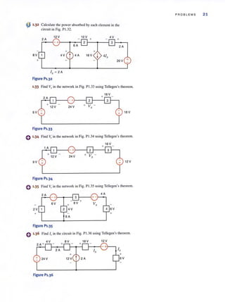
to represent currcnt flow is shown in Fig. J.2. I[ = 2 A in Fig. 1.2a indicates that at any point
in the wire shown, 2 C of charge pass from left to right each second. I']. = - 3 A in Fig. 1.2b
indicates that at any point in the wire shown, 3 C of charge pass from right to left each second.
Therefore, it is important to specify not only the magnitude of the variable representing the
current, but also its direction.](https://image.slidesharecdn.com/basicengineeringcircuitanalysis9thirwin-160630150938/85/Basic-engineering-circuit-analysis-9th-irwin-18-320.jpg?cb=1719934140)
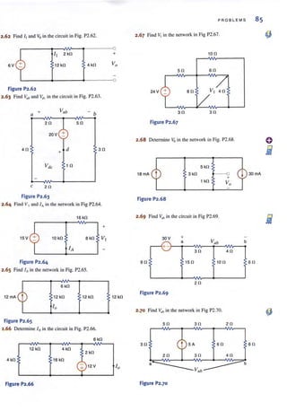
![SECT I ON 1.2
Switch
- Battery
Light bulb
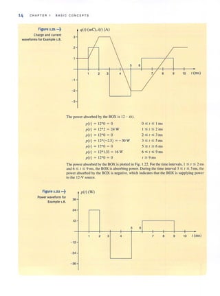
At this point we have presented the conventions that we employ in our discussions of
current and voltage. Ellergy is yet another important tenn of basic significance. Let's
investigate the voltage-current relationships for energy transfer using the flashlight shown in
Fig. 1.7. The basic elements of a flashlight are a battery, a switch, a light bulb, and connect-
ing wires. Assuming a good battery, we all know thutthe light bul b will glow when the switch
is closed. A current now flows in this closed circuit as charges flow out of the positive ter-
minal of the battery through the switch and light bulb and back into the negative terminal of
the battery. The current heats up the filament in the bulb, causing it to glow and emit light.
The light bulb converts electrical energy to thermal energy; as a result, charges passing
through the bulb lose energy. These charges acquire energy as they pass through the battery
as chemical energy is converted to electrical energy. An energy conversion process is occur-
ring in the flashlight as the chemical energy in the banery is converted to electrical energy,
which is then converted to thermal energy in the light bulb.
I
- BaHery
- Vbauery + + V bu1b -
Let's redraw the flashlight as shown in Fig. 1.8. There is a current I flowing in this dia-
gram. Since we know that the light bulb uses energy, the charges coming out of the bulb have
less energy than those entering the light bulb. In other words, the charges expend energy as
they move through the bulb. This is indicated by the voltage shown across the bulb. The
charges gain energy as they pass through the banery, which is indicated by the voltage across
the battery. Note the voltage--<:urrent relationships for the battery and bulb. We know that the
bulb is absorbing energy; the current is entering the positive terminal of the voltage. For the
battery, the current is leaving the positive temlinal, which indicates that energy is being
supplied.
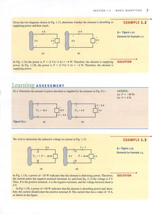
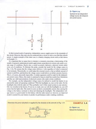
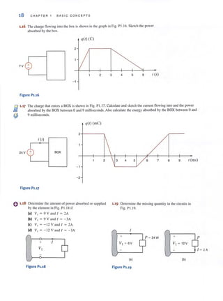
This is further illustrated in Fig. 1.9 where a circuit element has been extracted from a
larger circuit for examination. In Fig. 1.9a, energy is being supplied to the element by
whatever is attached to the terminals. Note that 2 A, that is, 2 C of charge are moving from
point A to point B through the element each second. Each coulomb loses 3 J of energy as it
passes through the element from point A to point B. Therefore, the element is absorbing 6 ]
of energy per second. Note that when the element is absorbing energy. a positive current
enters the positive terminal. In Fig. 1.9b energy is being supplied by the clement to whatever
is connected to terminals A-B. In this case, note that when the element is supplying energy,
a positive current enters the negative terminal and leaves via the positive terminal. In this con-
vention, a negative current in one direction is equivalent to a positive current in the opposite
direction, and vice versa. Similarly, a negative voltage in one direction is equivalent to a pos-
itive voltage in the opposite direction.
BASIC QUANTITIE S
~••• Figure 1.7
Flashlight circuit.
~... Figure 1.8
Flashlight circuit with
voltages and current.
A 1 ~ 2A
+
3V
B 1 ~ 2A
(a)
A 1 ~ 2A
+
3V
B I ~ 2 A
(b)
5
.or" Figure 1.9
Voltage- current relationships
for <aJ energy absorbed and
(bJ energy supplied.](https://image.slidesharecdn.com/basicengineeringcircuitanalysis9thirwin-160630150938/85/Basic-engineering-circuit-analysis-9th-irwin-21-320.jpg?cb=1719934140)
![•
6 C H APT ER 1 BASIC CONC E PTS
EXAMPLE 1.1
•
SOLUTION
Figure 1.10 ···t
Diagram for Example 1.1.
i(l)
+
V(I)
• -<••
Figure 1.11 i
Sign convention for power.
[hint ]
The passive sign convention
is used to determine whether
power is being absorbed or
supplied.
Suppose that your car will not start. To determine whether the battery is faulty, you turn on
the light switch and fi nd that the lights are very dim, indicating a weak battery. You borrow
a friend's car and a set of jumper cables. However, how do you connect his car's battery to
yours? What do you want his batlery to do?
Essentially, his car's battery must supply energy to yours, and therefore it should be
connected in the manner shown in Fig. J. IO. Note that the positive current leaves the posi-
tive termi nal of the good battery (supplyi ng energy) and enters the positive terminal of the
weak battery (absorbing energy), Note that the same connections are used when charging a
battery.
I
I
In practical applications there are often considerations other than simply the electrical
relations (e.g., safety). Such is the case with jump-starting an automobile. Automobile
batteries produce explosive gases that can be ignited accidentally, causing severe physical
injury. Be safe-follow the procedure described in your auto owner's manual.
We have defined voltage in joules per coulomb as the energy required to move a positive
charge of I C through an element. If we assume that we are dealing with a di fferential alllount
of charge and energy, then
li1V
v=-
dq
Muhiplying this quantity by the current in the element yields
1.2
1.3
which is the time rale of change of energy or power measured in joules per second, or watts
(W). Since, in general, both v and i are functions of time, p is also a time-varying quantity.
Therefore, the change in energy from time I, to lime 12 can be found by integrati ng Eq. ( 1.3);
that is,
1', 1"t.w = P dl = VillI
'1 '1
1.4
At this point, leI us summarize our sign convention for power. To determine the sign of
any of the quantities involved, the variables for the current and voltage should be arranged as
shown in Fig. 1. 11 . The variable for the voltage V{ /) is defi ned as the voltage across the ele-
ment with the positive reference at the same termi nal that the current variable i{/ ) is entering.
This convention is called the passive sign cOllvelllioll and will be so noted in the remainder
of this book. The product of V and i, with their attendant signs, will determine the magnitude
and sign of the powcr. If the sign of the power is positive, power is being absorbed by the ele-
ment; if the sign is ncgative. power is being supplied by the element.](https://image.slidesharecdn.com/basicengineeringcircuitanalysis9thirwin-160630150938/85/Basic-engineering-circuit-analysis-9th-irwin-22-320.jpg?cb=1719934140)
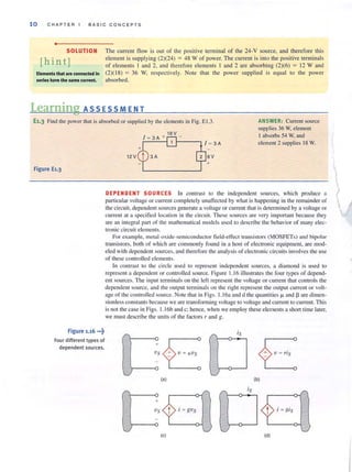

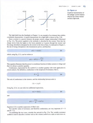
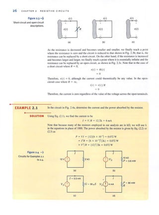
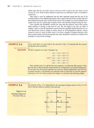
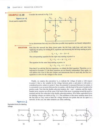
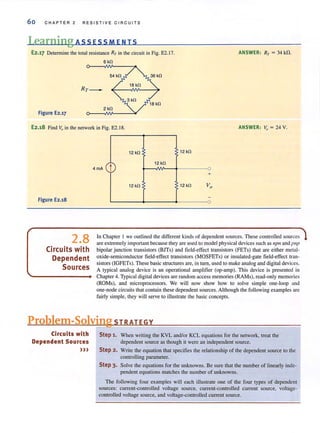
![36 C HAPTER 2 RESISTIVE C I RCUIT S
• SOLUTION The two KVL equations are
VR, + VR, - Vs = 0
20VR, + VR, - VR, = 0
Learning ASS ESS MEN IS
E2.6 Find ~ul and V'b in the network in Fig. E2.6. ANSWER: V.d = 26 V.
V,b = IOV.
6V
Figure E2.6
E2.7 Find Vbd in the circuit in Fig. E2.7. ANSWER: Vbd = II V.
12 V
Figure E2.7
[hint]
The subtleties associated
with Ohm's law, as described
here, are important and must
be adhered to in orderto
ensure that the variables
have the proper sign.
Figure 2.14 •••~
Circuits used to explain
Ohm's law.
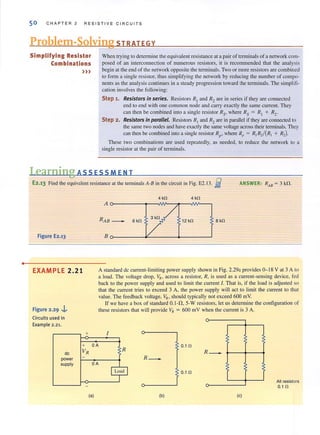
Before proceeding with the analysis of simple circuits, it is extremely important that we
emphasize a subtle but very critical point. Ohm's law as defined by the equation V :;; I R
refers to Lhe relationship between the voltage and current as defined in Fig. 2.14a. If the direc-
tion of either the current or the voltage, but not both, is reversed, the relationship between the
current and the voltage would be V :;; - IR. In a similar manner, given the circuit in
Fig. 2.14b. if the polarity of the voltage between the terminals A and 8 is specified as shown,
then the direction of the current I is from point B through R to point A. Likewise, in
Fig. 2. 14c, if the direction of the current is specified as shown, then the polarity of the voltage
must be such that point D is at a higher potential than point C and, therefore, the arrow rep-
resenting the voltage V is from point C to point D.
A I A R I
+
V R V R - -V-
C D
+ I
.J
B
.J
B
(a) (b) (c)](https://image.slidesharecdn.com/basicengineeringcircuitanalysis9thirwin-160630150938/85/Basic-engineering-circuit-analysis-9th-irwin-52-320.jpg?cb=1719934140)
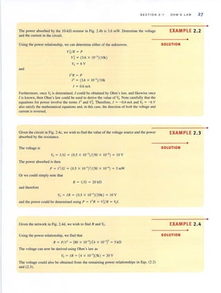
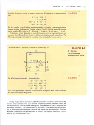
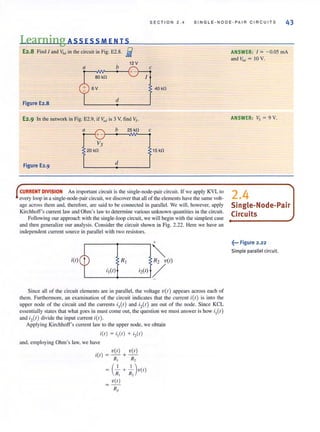
![SECTION 2 . 3 SINGLE·LOOP C I RCUITS 37
VOLTAGE DIVISION At this point we can begin to apply the laws we have presented
earlier to the analysis of simple circuits. To begin, we examine what is perhaps the simplest
circuit- a single closed path, or loop, of elements.
Applying KCL to every node in a single-loop circuit reveals that the same current flows
through all elements. We say that these elements are connected in series because they carry
the same Cllrrenl. We will apply Kirchhoff's voltage law and Ohm's law to the circuit to
determine various quantities in the circuit.
Our approach will be to begin with a simple circuit and then generalize the analysis to more
complicated ones.The circuit shown in Fig. 2.15 will serve as a basis for discussion. This cir-
cuit consists of an independent voltage source that is in series with two resistors. We have
assumed that the current flows in a clockwise direction. If this assumption is correct, the
solution of the equations that yields the current will produce a positive value. If the current is
actually flowing in the opposite direction, the value of the current variable will simply be
negative, indicating that the current is flowing in adirection opposite to that assumed. We have
also made voltage polarity assignments for VR1 and VR
2
' These assignments have been made
using the convention employed in ourdiscussion of Ohm's law and our choice for the direc-
tion of i(t }-that is, the convention shown in Fig. 2.14a.
or
Applying Kirchhoff's voltage law to this circuit yields
- v(t} + vN, + vN, = 0
V(t) = vN, + vN,
However, from Ohm's law we know that
vN, = Ri(t)
vN, = R,i(t)
Therefore,
V(t) = RJi(t ) + R2i(t)
Solving the equation for itt ) yields
2,9
Knowing the current, we can now apply Ohm's law to determine the voltage across each
resistor:
VN, = R,i(t )
= RJ[ v(t) ]
R, + R,
2.10
R,
= R, + R, v(t)
Similarly,
2.11
Though simple, Eqs. (2. 10) and (2.11) are very important because they describe the oper-
ation of what is called a voltage divider. In other words, the source voltage v(t} is divided
between the resistors Rl and R2 ill direct proportion to their resistances.
In essence, if we are interested in the voltage across the resistor RII we bypass the calcu-
lation of the current i(t) and simply multiply the input voltage v(t} by the ratio
R,
As illustrated in Eq. (2. 10), we are using the current in the calculation, but not explicitly.
2.3
Single-Loop
Circuits
itt)
v(t} +
'i' Figure 2,15
Single·loop circuit.
[hin tj
RI
R2
The manner in which voltage
divides between two
series resistors.
+
VRJ
+
vR,](https://image.slidesharecdn.com/basicengineeringcircuitanalysis9thirwin-160630150938/85/Basic-engineering-circuit-analysis-9th-irwin-53-320.jpg?cb=1719934140)

= 2.25 V
Now suppose that the variable resistor is changed from 90 kfl to 15 kfl. Then
V, = [30k3~kI5k]9
=6V
The direct voltage-divider calculation is equivalent to determining the current I and
then using Ohm's law to find 11,. Note that the larger voltage is across the larger resist-
ance. This voltage-divider concept and the simple circuit we have employed to describe it
are very useful because, as will be shown later, more complicated circuits can be reduced
to this form.
Finally, let us determine the instantaneous power absorbed by the resistor R2under the
two conditions R, = 90 kfl and R, = 15 kfl. For the case R, = 90 kfl, the power absorbed
by R, is
( 9 )'P, = I ' R, = 120k (30k)
= O.169mW
In the second case
P, = (4~J'(30k)
= 1.2 mW
The current in the first case is 75 fl.A, and in the second case it is 200 fl.A. Since the
power absorbed is a function of the square of the current, the power absorbed in the two
cases is quite different.](https://image.slidesharecdn.com/basicengineeringcircuitanalysis9thirwin-160630150938/85/Basic-engineering-circuit-analysis-9th-irwin-54-320.jpg?cb=1719934140)
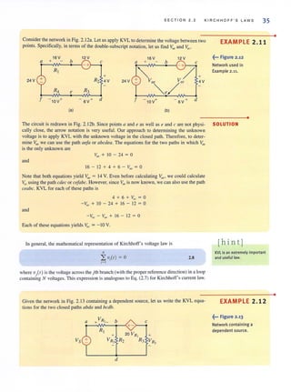
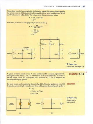
![SE CT ION 2.3 SINGLE-LOOP CIRCUITS 39
Let us now demonstrate the practical utility of this simple voltage-divider network.
Consider the circuit in Fig. 2.17a, which is an approximation of a high-voltage de transmis-
sion facility. We have assumed that the bottom p0l1ion of the transmission line is a perfect
conductor and will justify this assumption in the next chapter. The load can be represented by
a resistor of value 183.5 n. Therefore, the equivalent circuit of this network is shown in
Fig.2.17h.
Line resistance is 0.04125 nlmile
16.5 fl +
Load 400 kV 183.5 fl
Perfect conductor
400-mile transmission line
(a) (b)
Let us determine both the power delivered to the load and the power losses in the line.
Using voltage division, the load voltage is
V. - [ 183.5 ]400k
'rod - 183.5 + 16.5
= 367 kY
The input power is 800 MW and the power transmitted to the load is
= 734MW
Therefore, the power loss in the transmission line is
= 66MW
Since P = VI , suppose now that the utility company supplied power at 200 kY and 4 kA. What
effect would this have on our transmission network? Without making a single calculation, we
know that because power is proportional to the square of the current, there would be a large
increase in the power loss in the line and, therefore, the efficiency of the facility would decrease
substantially. That is why, in general, we transmit power at high voltage and low current.
MULTIPLE-SOURCE/RESISTOR NETWORKS At this point we wish to extend our
analysis to include a multiplicity of voltage sources and resistors. For example, consider the
circuit shown in Fig. 2. 18a. Here we have assumed that the current flows in a clockwise
direction, and we have defined the variable i(l) accordingly. This mayor may not be the
case, depending on the value of the various voltage sources. Kirchhoff's voltage law for this
circuit is
+VR, + V,(/) - V,( /) + vR, + V,( /) + V,(/ ) - V,(/) = 0
or, lIsing Ohm's Jaw,
(R, + R,)i(/) = V,(/) - V,(/) + V)(/) - V,( /) - V,(/)
which can be written as
EXAMPLE 2.14
~... Figure 2.17
A high·voltage de
transmission facility.
•
SOLUTION
•](https://image.slidesharecdn.com/basicengineeringcircuitanalysis9thirwin-160630150938/85/Basic-engineering-circuit-analysis-9th-irwin-55-320.jpg?cb=1719934140)
![40 CHAPTER 2 RESISTI V E C I RC U IT S
Figure 2.18 "'f
Equivalent circuits with
multiple sources.
+ VRI _
RI
itt)
v(t) +
RN
- VR
N
+
Figure 2.19 ."f"
Equivalent circuits.
where
v(t ) = v,(t ) + 'U,(t) - [v,(t) + 'U,(t) + v,(t)]
so that under the preceding definitions, Fig. 2.18a is equivalent to Fig. 2.18b. In other words,
the sum of several voltage sources in series can be replaced by onc source whose value is the
algebraic sum of the individual sources. This analysis can, of course, be generalized to a cir-
cuit with N series sources.
i(t)+VR, _ vz(t)
R,
v} (t) + v3(t)
+
itt) RI
+
vs(t) +
Rz V R2 v(t) R2
- +
V4(t)
(a) (b)
+ V R2_ + VR]_
R2 R3
+
R4 VR,
itt)
+
Rs VR, 'U(t) Rs = R} + R2 + R3 +... + RN
(a) (b)
Now consider the circuit with N resistors in series, as shown in Fig. 2.19a. Applying
Kirchhoff's voltage law to this circuit yields
and therefore,
where
and hence,
v( t) = vRI + VN~ + ... + 'UN".
= R,i(t ) + R,i(t) + ... + R,vi(t )
v(t ) = Rsi(t )
v(t )
itt ) = -
Rs
2.12
2.13
2.14](https://image.slidesharecdn.com/basicengineeringcircuitanalysis9thirwin-160630150938/85/Basic-engineering-circuit-analysis-9th-irwin-56-320.jpg?cb=1719934140)
![•
44 C H A PTER 2 RE S I S TI V E CI RC U ITS
[hint]
The parallel resistance
equation.
[hint]
The manner in which
current divides between
two parallel resIstors.
EXAMPLE 2.17
•
where
R =p
2. 16
2.17
Therefore, the equivalent resistance of two resistors connected in parallel is equal to the
product of their resistances divided by their sum. Note also that this equivalent resistance Rp
is always less than either RJ
or R2. Hence, by connecting resistors in parallel we reduce the
overall resistance. In the special case when RJ
= R2• the equivalent resistance is equal 10 half
of lhe value of lhe individual resislors.
The manner in which the current i(r) from the source divides between the two branches
is called currelIl division and can be found from the preceding expressions. Forexample,
and
and
V(I) = Rpi(l)
R,R, i(l)
RI + R2
V(I)
i,(I) = -
R,
R,
i,(I ) = - i(l )
R, + R,
i,(I)
V( I)
R,
R,
R, + R, i(l)
Equalions (2. 19) and (2.20) are malhematical statemenls of lhe current-division rule.
Given the network in Fig. 2.23a, let us find I" I" and yo.
2.1S
2.19
2.20
SOLUTION First, il is important to recognize that the current source feeds two parallel paths. To empha-
size lhis point, the circuit is redrawn as shown in Fig. 2.23b. Applying current division,
we obtain
I = [ 40k + SOk ](0 x 10-' )
, 60k + (40k + 80k) .9
= 0.6 mA
and
I = [ 60k ](0 9 X 10-')
, 60k + (40k + SOk) .
= 0.3 rnA
Note that the larger current flows through the smaller resistor, and vice versa. In addition,
nOle that if lhe resistances of lhe two paths are equal, the current will divide equally belween
them. KCL is satisfied since II + 12 = 0.9 rnA.
The voltage Vo can be derived using Ohm's law as
Vo = SOkI,
= 24 V](https://image.slidesharecdn.com/basicengineeringcircuitanalysis9thirwin-160630150938/85/Basic-engineering-circuit-analysis-9th-irwin-60-320.jpg?cb=1719934140)
![or
where
SECT ION 2 . 4
i"(,) = i,(,) + i,(I) + ... + iN(I)
= (~ + ~ + ... + _I )V(I)
R] Rl RN
v(I)
io(l) = -
R"
1 N I
- = ~ -
Rp i= ] Rj
SINGLE·NODE·PAIR CIRCUITS
2.21
2.22
2.23
so that as far as the source is concerned, Fig. 2.26a can be reduced to an equivalent circuit,
as shown in Fig. 2.26b.
The current division forany branch can be calculated using Ohm's law and the preceding
equations. For example, for the jth branch in the network of Fig. 2.26a,
Using Eq. (2.22). we obtain
iJI) = V~)
J
. R" .
'j(l ) = - '.,(1)
Rj
which defines the current-division rule for the general case.
2.24
47
Given the circuit in Fig. 2.27a, we wish to find the current in the 12-kD load resistor. EXAMPLE 2.19
To simplify the network in Fig. 2.27a, we add the current sources algebraically and combine SOLUTION
the paraliel resistors in the following manner:
1 I I I
- =-+ -+-
Rp 18k 9k 12k
R" = 4 kn
Using these values we can reduce the circuit in Fig. 2.27a to that in Fig. 2.27b. Now,
applying current division, we obtain
I, = -[ 4k ] (1 X 10⁻³)
4k + 12k
= - O.25 mA
18 kn 9 kn 12 kn
(al
4 kn
(bl
l' Figure 2.27
Circuits used in
Example 2.19.
•
12 kn
•](https://image.slidesharecdn.com/basicengineeringcircuitanalysis9thirwin-160630150938/85/Basic-engineering-circuit-analysis-9th-irwin-63-320.jpg?cb=1719934140)
![•
•
52 CHAP TE R 2 RES I S TI VE CI R CU IT S
TABLE 2.1 Standard resistor values for 5% and 10% tolerances (values available with a 10%
tolerance shown in boldface)
1.0 10 100 t.ok 10k took l.oM 10M
1.1 11 110 1.1k 11k l10k 1,1M 11M
1.2 12 120 1.2k 12k 120k 1.2M 12M
1·3 13 130 1·3k 13k 130k 1·3M 13M
1·5 15 150 1·5k 15k 150k 1·5M 15M
1.6 16 160 1.6k 16k 160k 1.6M 16M
1.8 18 180 1.8 k 18k t8ak 1.8M IBM
2.0 20 200 2.ok 20k 200k 2.oM 20M
2.2 22 22. 2.2k 22k 2 20k 2.2M 22M
2·4 24 240 2·4k 24k 2ltok 2·4M
2·7 27 270 2·7k 27k 270k 2·7M
3·0 30 300 3·0k 30k Jook 3·0M
].3 33 330 ].3k 33k 330k ].3M
3.6 36 360 3·6k 36k 360k 3·6M
J.9 39 390 3·9k 39k 390k J.9M
4·3 43 430 4·3k 43k 430k 4·3M
4-7 47 470 4-]k 47k 470k 4-]M
5.1 51 510 5·1k 51k S10k 5·1M
5.6 56 560 5·6k 56k S60k 5·6M
6.2 62 620 6.2k 62k 620k 6.2M
6.8 68 680 6.8 k 68 k 680k 6.8 M
7·5 75 750 7·5k 75k 750k 7·5M
8.2 82 820 8.2k 82k 820k 8.2M
9·1 91 910 9·1k 91k 910k 9·1M
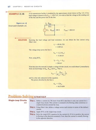
EXAMPLE 2.22 Given the network in Fig. 2.30. we wish to find the range for both the current and power
dissipation in the resistor if R is a 2.7-kO resistor with a tolerance of 10%.
•
10V
SOLUTION Using the equations 1= VIR = 10/R and P = V'/R = 100/R. the minimum and maxi-
mum values for the resistor, current, and power are outlined next.
I Minimum resistor value = R(I - 0.1) = 0.9 R = 2.43 kO
Maximum resistor value = R( I + 0.1) = 1.1 R = 2.97 kO
Minimum current value = 10/2970 = 3.37 rnA
R Maximum current value = 10/2430 = 4.12 rnA
Minimum power value = 100/2970 = 33.7 mW
Maximum power value = 100/2430 = 41.2 mW
Figure 2.301" Thus. the ranges for the current and power are 3.37 rnA to 4.12 rnA and 33.7 mW to
Circuit used in Example 2.22. 41.2 mW. respectively.
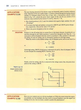
EXAMPLE 2.23 Given the network shown in Fig. 2.31 : (a) find the required value for the resistor R; (b) use
Table 2.1 to select a standard 10% tolerance resistor for R; (c) using the resistor selected in
(b). determine the voltage across the 3.9-kO resistor; (d) calculate the percent error in the
voltage I'l. if the standard resistor selected in (b) is used; and (e) determine the power rat-
ing for this standard component.](https://image.slidesharecdn.com/basicengineeringcircuitanalysis9thirwin-160630150938/85/Basic-engineering-circuit-analysis-9th-irwin-68-320.jpg?cb=1719934140)
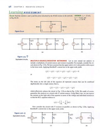
![SECT I ON 2.6 CIRCUITS W IT H SERIE S - PAR ALLEL COMBINAT IONS OF RESISTORS
or, since Vbis equal to the voltage drop across the 3-kfl resislOr, we could use Ohm's law as
Vb = 3k/3
3
= - v
2
We are now in a position to calculate the final unknown currents and voltages in Fig. 2.32a.
Knowing Vh' we can calculate '4using Ohm's law as
VI}= 4kI4
3
2
14 = -
4k
3
= g mA
Then, from Kirchhoff's current law, we have
1
-x
2
I) = 14 + Is
10-3 = ~ X 10-3 + I,
8
1
Is = - rnA
. 8
We could also have calculated Is using the current-division rule. For example,
Finally, ~ can be computed as
4k
I - f
5 - 4k + (9k + 3k) 3
1
= - rnA
8
V, = 1,(3k)
3
= -v
8
~. can also be found using voltage division (i.e., the voltage Vbwill be divided between the
9-kD and 3-kD resistors), Therefore,
[
3k ]V - V
, - 3k+9k b
3
=-v8
Note that Kirchhoff's current law is satisfied at every node and Kirchhoff's voltage law
is satisfied around every loop, as shown in Fig. 2.32d.
The following example is, in essence, the reverse of the previous example in that we
are given the current in some branch in the network and are asked to find the value of the
input source.
55](https://image.slidesharecdn.com/basicengineeringcircuitanalysis9thirwin-160630150938/85/Basic-engineering-circuit-analysis-9th-irwin-71-320.jpg?cb=1719934140)
![58 CHAPTER 2 RESISTI V E CI R C U ITS
Consider the networks shown in Fig. 2.35. Note that the resistors in Fig. 2.35a form a
Ll. (delta) and the resistors in Fig. 2.35b form a Y (wye). If both of these contiguralions are
coonected at only three terminals a, b, and c, it would be very advantageous if an equivalence
could be established between them. It is, in fact, possible to relate the resistances of one net-
work to those of the other such that their terminal characteristics are the same. This relation-
shi p between the Iwo network configurations is called the y-.o. transformation.
The transformation that relates the resistances RI ' R2. and R] to the resistances R(l' Rh, and
Rc is derived as follows. For the two networks to be equivalent at each corresponding pair of
terminals, it is necessary that the resistance at the corresponding tenninals be equal (e.g., the
resistance at terminals a and b with c open-circuited must be the same for both networks).
Therefore, if we equate the resistances for each corresponding set of terminals, we obtain
the following equations:
R"b = R" + R" =
RIK = Rb + R,.
R,(R, + R,)
R, + II, + II,
R,(R, + II, )
R) + Rl + R2
Solving th is set of equations for Ra , Rh , and Rc yields
Similarly, if we solve Eg. (2.27) for R
"
R2, and R3, we obtain
RaR" + R"R, + R"Rc
II,
R) = _R~,_R"b_+_R-,b:cR-",_+_R-",-,R""
II,
2.27
2.28
2.29](https://image.slidesharecdn.com/basicengineeringcircuitanalysis9thirwin-160630150938/85/Basic-engineering-circuit-analysis-9th-irwin-74-320.jpg?cb=1719934140)
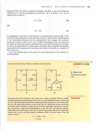
![S E C TI ON 2 . 8 CIR CUI TS W ITH DEP E ND E N T SOU R C E S 61
Let us determine the voltage V. in the circuit in Fig. 2.37.
h 3 kn
.-~~----~-+.>--+----~
12 V
Va = 2000 I I
5 kn
+
~--------------~---~o
Applying KYL, we obtain
- 12 + 3k/l - VA + 5k/l = 0
where
and the units of the multiplier, 2000, are ohms. Solving these equations yields
11 = 2 rnA
Then
v. = (5 k)/1
= lOY
Given the circuit in Fig. 2.38 containing a current·controlled currenl source, let us find the
voltage Vo.
2 kn
4 kn
Applying KCL at the top node, we obtain
where
" "10 X 10-3 + S + ~ - 4/. = 0
2k + 4k 3k
Vs
1 = -
• 3k
Substituting this expression for the controlled source into the KCL equation yields
10-2 + Vs + Vs _ 4Vs = 0
6k 3k 3k
Solving this equation for Vs, we obtain
Vs = 12 Y
The voltage Vo can now be obtained using a simple voltage divider; that is,
V. - "[
4k ]
. - 2k+4k s
= 8Y
EXAMPLE 2.27
~... Figure 2.37
Circuit used in Example 2.27.
•
SOLUTION
EXAMPLE 2.28
~... Figure 2.38
Circuit used in Example 2.28.
•
SOLUTION
•
•](https://image.slidesharecdn.com/basicengineeringcircuitanalysis9thirwin-160630150938/85/Basic-engineering-circuit-analysis-9th-irwin-77-320.jpg?cb=1719934140)
![70 CHAPTER 2 RESISTIVE CIRCUITS
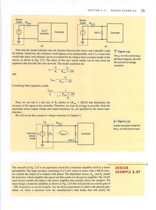
Figure 2.47 ••.~
The Wheatstone bridge
circuit.
Engineers also use this bridge circuit to measure strain in solid material. For example, a
system used to determine the weight of a truck is shown in Fig. 2.48a. The platform is sup-
ported by cylinders on which strain gauges are mounted. The strain gauges, which measure
strain when the cylinder deflects under load, are connected to aWheatstone bridge as shown
in Fig. 2.4Sb. The strain gauge has a resistance of 120 n under no-load conditions and
changes value under load. The variable resistor in the bridge is acalibrated precision device.
Weight is determined in the following manner. The AR3required to balance the bridge
represents the ~ strain, which when multiplied by the modulus of elasticity yields the
~ stress. The ~ stress multiplied by the cross-sectional area of the cylinder produces the
tJ. load, which is used to determine weight.
Let us determine the value of R3underno load when the bridge is balanced and its value
when the resistance of the strain gauge changes to 120.24 nunder load.
1 1 - - - - - - - -
SOLUTION Using the balance equation for the bridge, the value of R, at no load is
Figure 2.48 •••~
Diagrams used in
Example 2.33.
Under load, the value of R, is
Therefore, the ~R3 is
R,= (;:)Rx
C~~)(120)
109.0909 n
R, = C~~)(12024)
= 109.3091 n
tJ.R, = 109.3091 - 109.0909
= 0.2182 n
~____ Platform
G1+----- Strain gauge -----H;;]
(a)
(b)
Strain gauge
R,](https://image.slidesharecdn.com/basicengineeringcircuitanalysis9thirwin-160630150938/85/Basic-engineering-circuit-analysis-9th-irwin-86-320.jpg?cb=1719934140)
![SEC TI O N 2.11 DES IG N E XAMP LE S 71
Most of this text is concerned with circuit analysis; that is, given a circuit in which all the
components are specified. analysis involves finding such things as the voltage across some
element or the current through another. Furthermore, the solution of an analysis problem is
generally unique. In contrast, design involves determining the circuit configuration that will
meet certain specifications. In addition, the solution isgenerally not unique in that there may
be many ways to satisfy the circuit/performance specifications. It is also possible that there
is no solution that will meet the design criteria.
In addition to meeting certain technical specifications. designs normally must also meet
other criteria, such as economic, environmental, and safety constraints. For example, if a cir-
cuit design that meets the technical specifications is either too expensive or unsafe, it is not
viable regardless of its technical merit.
At thispoint, the number of elements that we can employ in circuit design islimited prima-
rily to the linear resistor and the active elements we have presented. However, as we progress
through the text we will introduce a number of other elements (for example, the op-amp,
capacitor, and inductor), which will significantly enhance our design capability.
We begin our discussion of circuit design by considering a couple of simple examples that
demonstrate the selection of specific components to meet certain circuit specifications.
An electronics hobbyist who has built his own stereo amplifier wants to add a back-lit dis-
play panel to his creation for that professional look. His panel design requires seven light
bulbs-two operate at 12 V/ 15 mA and five at 9 V/ 5 rnA. Luckily, his stereo design already
has a quality 12-V dc supply; however, there is no 9-V supply. Rather than building a new
dc power supply, let us use the inexpensive circuit shown in Fig. 2.49a to design a 12-V to
9-V converter with the restriction that the variation in V2 be no more than ±S%. In particu-
lar, we must determine the necessary values of RJ and R2·
First, lamps L, and L, have no effect on V,. Second, when lamps L,-L., are on, they each
have an equivalent resistance of
V, 9
R,q = I = 0.005 = 1.8 k!1
As long as V1
remains fairly constant, the lamp resistance will also be fairly constant. Thus,
the requisite model circuit for our design is shown in Fig. 2.49b. The voltage V2 will be at
its maximum value of 9 + 5% = 9.45 V when L;-L., arc all off. In this case R, and R, are
in series, and ~ can be expressed by simple voltage division as
V, = 9.45 = 12[ R, ]
- RJ
+ R2
Re-arranging the equation yields
~ = 0.27
R,
A second expression involving RJ
and R2can be developed by considering the case when
L;-L., are all on, which causes V, to reach its minimum value of 9- 5%, or 8.55 V. Now, the
effective resistance of the lamps is five 1.8-k!1 resistors in parallel, or 360 !1. The corre-
sponding expression for ~ is
V, = 8.55 = [
R,//360 ]
12 -
R, + (R,//360)
which can be rewritten in the form
360R, + 360 + R,
R, 12
--'-''------ = - = 1.4
360 8.55
2.11
Design Examples
DESIGN
EXAMPLE 2.34
•
SOLUTION
•](https://image.slidesharecdn.com/basicengineeringcircuitanalysis9thirwin-160630150938/85/Basic-engineering-circuit-analysis-9th-irwin-87-320.jpg?cb=1719934140)
![•
72 CHAPTER 2 RESISTIVE CIRCUITS
figure 2.49 .-~
12-V to 9-V converter circuit
for powering panel lighting.
DESIGN
EXAMPLE 2.35
•
12 V +
12 V +
+
R2 V2
+
R2 V2
1.8 kO 1.8 kO
(a)
1.8 kO
(b)
Ls
1.8 kO 1.8 kO
Substituting the value determined for RI/ R2 into the preceding equation yields
R, = 360[1.4 - I - 0.27]
or
R, = 48.1 fl.
and so for R2
R, = 178.3 fl.
Let's design a circuit that produces a 5-V output from a 12-V input. We will arbitrarily fix
the power consumed by the circuit at 240 mW. Finally, we will choose the best possible
standard resistor values from Table 2.1 and calculate the percent error in the output voltage
that results from that choice.
SOLUTION The simple voltage divider, shown in Fig. 2.50, is ideally suited for this application. We
know that ~ is given by](https://image.slidesharecdn.com/basicengineeringcircuitanalysis9thirwin-160630150938/85/Basic-engineering-circuit-analysis-9th-irwin-88-320.jpg?cb=1719934140)
![SECTION 2 . 11 DESIGN EXAMPLES
73
which can be written as
[
V;, ]RJ = R, Vo - I
Since all of the circuit's power is supplied by the 12-V source, the total power is given by 12V +
_~V-",rn,-
P = R -< 0.24
1+ R2
Using the second equation to eliminate RIl we find that R2has a lower limit of
VoV;, (5)(12 )
R '" - - = - - - = ?50 0, P 0.24 -
1'" Figure 2·50
A simple voltage divider
Substituting these results into the second equation yields the lower limit of RI1 that is
RJ = R2[~: - I] '" 350 0
Thus, we find that a significant portion of Table 2.1 is not applicable to this design.
However, determining the best pair of resistor values is primarily a trial-and-error operation
that can be enhanced by using an Excel spreadsheet as shown in Table 2.4. Standard resis-
tor values from Table 2.1 were entered into Column A of the spreadsheet for R,. Using the
equation above, theoretical values for Rl were calculated using Rl = 1.4 ·R2. A standard
resistor value was selected from Table 2.1 for RJ
based on the theoretical calculation in
Column B. Vo was calculated using the simple voltage-divider equation, and the power
absorbed by RJ
and R, was calculated in Column E.
TABLE 2.4 Spreadsheet calculations for simple voltage divider
-------R2 Rl theor R1 Vo Pabs
2 300 420 430 4·932 0 .197
3 330 462 470 4·950 0.180
4 360 504 510 4.966 0.166
5 390 546 560 4·926 0.152
6 430 602 620 4·9'4 0.137
7 470 658 680 4.904 0.125
8 510 714 750 4.857 0.114
9 560 784 750 5·130 0.110
10 620 868 910 4.863 0 .094
11 680 952 910 5·132 0.091
12 750 1050 1000 5·143 0 .082
13 820 1148 1100 5 .125 0.075
'4 910 1274 1300 4·941 0.06 5
15 1000 1400 1300 5·217 0.0 63
16 1100 1540 1500 5·077 0.055
17 1200 1680 1600 5·143 0 .051
18 1300 1820 1800 5.032 0.046
19 1500 2100 2000 5.143 0.041
20 1600 2240 2200 5.0 53 0.038
21 1800 2520 2400 5·143 0.034
22 2000 2800 2700 5·106 0.031
23 2200 3080 3000 5·on 0 .028
24 2400 3360 3300 5·053 0.025
+
Vo = 5V](https://image.slidesharecdn.com/basicengineeringcircuitanalysis9thirwin-160630150938/85/Basic-engineering-circuit-analysis-9th-irwin-89-320.jpg?cb=1719934140)
![o
74 CHA P TER 2 RE S I STIVE CIRCUITS
DESIGN
EXAMPLE 2.36
Note that a number of combinations of R] and R2 satisfy the power constraint for this cir-
cuit. The power absorbed decreases as R, and R, increase. Let's select R, = 1800 n and
R, = 1300 n , because this combination yields an output voltage of 5.032 V that IS closest
to-the desired value of 5 V. The resulting error in the output voltage can be determined from
the ex.pression
[
5.032 - 5]
Percent error = 5 100% = 0.64%
It should be noted, however, that these resistor values arc nominal, thal is, typical values.
To find the worst-case error, we mllst consider that each resistor as purchased may be as much
as ±5%off the nominal value. In this application, since Vois already greater than the target of
5 V, the worst-case scenario occurs when Vo increases even further. that is, Rl is 5% too low
(17I0 n ) and R, is 5% too higb (1365 n ). The resulting output voltage is 5.32 V, which yields
a percent error of 6.4%. Of course, most resistor values are closer to the nominal value than
to the ouaranteed maximum/minimum values. However, if we intend to build this circuit withc
a guaranteed tight output error such as 5% we should lise resistors with lower tolerances.
How much lower should the tolerances be? Our first equation can be altered to yield the
worst-case output voltage by adding a tolerance, tJ., to R, and subtracting the tolerance from
RI
• Let's choose a worst-case output voltage of VOmax = 5.25 Y, that is, a 5% error.
[
R,(1 + 8 ) ] [ 1300(1 + 8 ) ]
VOm~ = 5.25 = It," RI
(1 _ 8 ) + R,( I + 8 ) = 12 1800( 1 - 8 ) + 1300(1 + 8 )
The resulting value of tJ. is 0.037, or 3.7%. Standard resistors are available in tolerances of
10, 5, 2, and I%. Tighter tolerances are available but very expensive. Thus, based on nom-
inal values of 1300 nand 1800 n,we should utilize 2% resistors to ensure an output volt-
age error less than 5%.
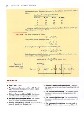
In factory instrumentation, process parameters such as pressure and flowrate are measured,
converted to electrical signals, and sent some distance to an electronic controller. The con-
troller then decides what actions should be taken. One of the main concerns in these sys-
tems is the physical distance between the sensor and the controller. An industry standard
format for encoding the measurement value is called the 4-20 rnA standard, where the
parameter range is linearly distributed from 4 to 20 mA. For example. a 100 psi pressure
sensor would output 4 rnA if the pressure were 0 psi, 20 rnA at 100 psi, and 12 rnA at 50 psi.
But most instrumentation is based on voltages between 0 and 5 Y, not on currents.
Therefore, let us design a current-to-voltage converter that will output 5 V when the cur-
rent signal is 20 mA.
•0- --- ---
SOLUTION The circuit in Fig. 2.51a is a very accurate model of our situation. The wiring from the sen-
sor unit to the controller has some resistance, Rwire ' If the sensor output were a voltage pro-
portional to pressure, the voltage drop in the l.ine would cause measurement error even if the
sensor output were an ideal source of voltage. But, since the data are contained in the cur-
rent value, Rwire does not affect the accuracy at the controller as long as the sensor acts as
an ideal current source.
As for the current-to-voltage converter, it is extremely simple-a resistor. For 5 V at
20 rnA, we employ Ohm's law to find
R = _ 5_ =250 n
0.02
The resulting converter is added to the system in Fig. 2.5 1b. where we tacitly assume that
the controller does not load the remaining portion of the circuit.](https://image.slidesharecdn.com/basicengineeringcircuitanalysis9thirwin-160630150938/85/Basic-engineering-circuit-analysis-9th-irwin-90-320.jpg?cb=1719934140)
![78 C H A PTE R 2 RE S I S T IV E C I RC UI TS
2.9 Many years ago a siring of Christmas tree lights was man-
ufactured in the form shown in Fig. P2.9a. Today the
lights are manufactured as shown in Fig. P2.9b. Is there a
good reason for this change?
: ®n------.,@--h-m-m~
(a)
: ¥ fn n~__________--'f
(b)
Figure P2.9
2.10 Find 11in the network in Fig. P2.IO
2mA
Figure P2.10
2.11 Find II in the network in Fig. P2. !1
6mA
4mA
Figure P2.11
2.12 Find I I in the network in Fig. P2. 12
I I
6mA
Figure P2.12
2 mA
2.13 Find 11and 12 in the circuit in Fig. P2. 13.
S mA
4 mA 2mA
Figure P2.13
2.14 Find I] in (he circuit in Fig. P2. 14.
I I
4 rnA
+
2mA
Figure P2.14
2.15 Find Ix in the circuit in Fig. P2. IS.
5 I,
LI.::x___-.4____-!.____..J 2 mA
Figure P2.15
2.16 Determine h in the circuit in Fig. P2. 16.
6 kfl 3 I, 2 kfl 3 kfl
Figure P2.16](https://image.slidesharecdn.com/basicengineeringcircuitanalysis9thirwin-160630150938/85/Basic-engineering-circuit-analysis-9th-irwin-94-320.jpg?cb=1719934140)

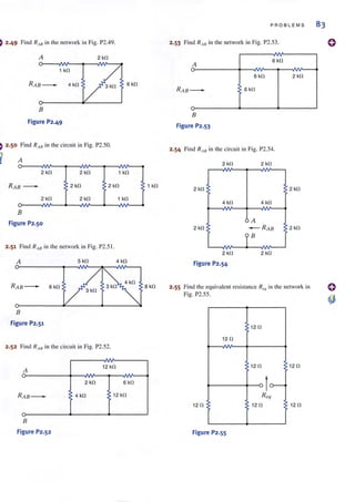
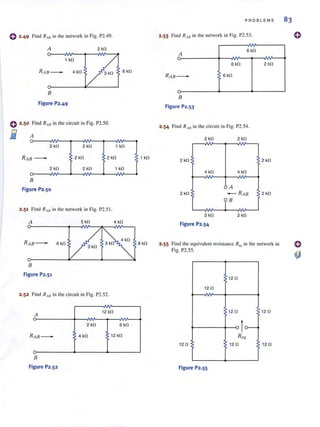
![o 2·49 Find RA8 in the network in Fig. P2.49.
A 2 kfl
1 kfl
RAB _ 4 kfl 3 kfl 6 kfl
B
Figure P2.49
=> 2·50 Find RA8 in the circuit in Fig. P2.50.
i A
~~~~~~~~#-4
2 kfl 1 kfl2kfl
RAB - 2 kfl 2 kfl
2 kfl 2 kfl H fl
B
Figure P2.50
2.51 Find RA8
in the network in Fig. P2.5 1.
A 5 kfl 4 kfl
4 kfl
3 kfl
3 kfl
6 kfl
B
Figure P2·51
" " F g po 50
F
" d R in the circUit 111 I . _ .-'
2.52 In A8
r 12 kfl
A
2 kfl
6 kfl
V"
4 kfl
12 kfl
RAB -
U"
B
Figure P2·52
1 kfl
8 kfl
PROBLEMS 83
2.53 Find R,w in the network ill Fig. P2.53.
A
-
B
Figure P2.53
:
6 kfl
6kfl
6 kfl
2.54 Find R AH in the circuit in Fig. P2.54.
2 kfl 2 kfl
2 kfl
4 kfl
2 kfl
2 kfl
Figure P2.54
4 kfl
v-
A
- RAB
]8
2kfl
2 kfl
2kfl
2 kfl
2·55
" R' the network inFind the equivalent resistance tq In
Fig. P2.55.
12 fl
12 fl
12 fl 12fl
-0
R e(f
12 !l
12 !l
Figure P2·55
o](https://image.slidesharecdn.com/basicengineeringcircuitanalysis9thirwin-160630150938/85/Basic-engineering-circuit-analysis-9th-irwin-99-320.jpg?cb=1719934140)

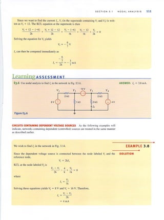
![98 C H APT E R 3 N O D AL AND LOO P ANALYS I S TECHN I OUES
[hint]
Employing the passive sign
convention.
Figure 3.4 •••~
A three-node ci rcuit.
The voltage VI = 4 V is the voltage at node 1 with respect to the reference node 3.
Similarly. the voltage V2 = - 2 V is the voltage at node 2 with respect to node 3. In addition,
however, the voltage at node 1 with respect to node 2 is +6 Y, and the voltage at node 2 with
respect to node 1 is - 6 V. Furthermore, since the current will flow from the node of higher
potential to the node of lower potential, the current in R1is from lOp to bottom, the current
in R2 is from left 10 right, and the current in R) is from bOllom to top.
These concepts have imporrant ramitications in our daily lives. If a man were hanging in
midair with one hand on one line and one hand on another and the dc line voltage of each
line was exactly the same, the voltage across his heart would be zero and he would be safe.
If, however, he let go of one line and let his feet touch the ground, the dc line voltage would
then exist from his hand to his foot with his heart in the middle. He would probably be dead
the instant his fool hit the ground.
In the (Own where we live, a young man tried to retrieve his parakeelthat had escaped its
cage and was outside sitting on a power line. He stood on a metal ladder and with a metal
pole reached for the parakeet; when the metal pole touched the power line, the man was killed
instantl y. Electric power is vital to our standard of living, but it is also very dangerous. The
material in this book does I/ ot qualify you to handle it safely. Therefore, always be extreme-
ly careful around electric circuits.
Now as we begin our discussion of nodal analysis, our approach will be to begin with sim-
ple cases and proceed in a systematic manner to those that are more challenging. Numerous
examples will be the vehicle used to demonstrate each facet of this approach. Finally, at the
end of this section, we will outline a strategy for attacking any circuit using nodal analysis.
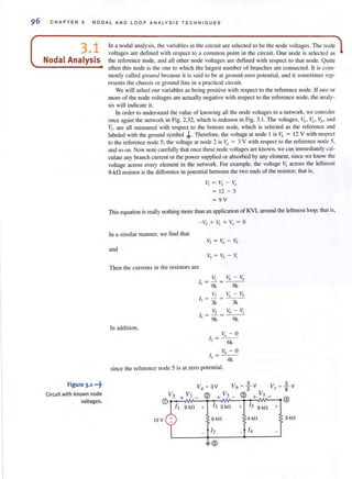
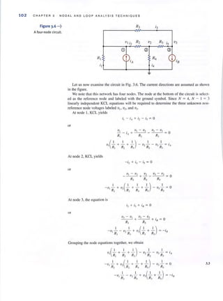
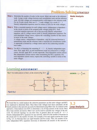
CIRCUITS CONTAINING ONLY INDEPENDENT CURRENT SOURCES Consider
the network shown in Fig. 3.4. Note that this network contains three nodes, and thus we know
that exactly N - I = 3 - I = 2 linearly independenl KCL equations will be required to
determine the N - I = 2 unknown node voltages. First, we select the bottom node as the
reference node, and then the voltage at the two remaining nodes labeled VI and V2 will be
measured with respect to this node.
The branch currents are assumed to flow in the directions indicated in the figures. If one
or more of the branch currents are actually flowing in a direction opposite to that assumed,
the analysis will simply produce a branch current that is negative.
Applying KCL at node I yields
- i" + i l + i 2 = 0
Using Ohm's law (i = G'v) and noting that the reference node is at zero potential, we obtain
- i. + G,(v, - 0) + G,(v, - v,) = 0
or
KCL at node 2 yields
or
- G,(v, - v,) + in+ G,(v, - 0) ~ 0
which can be expressed as
V I v2
CD '2 R2
'A R I
i I
= @](https://image.slidesharecdn.com/basicengineeringcircuitanalysis9thirwin-160630150938/85/Basic-engineering-circuit-analysis-9th-irwin-118-320.jpg?cb=1719934140)
![SECTION 3. 1
Therefore, the two equations for the two unknown node voltages VI and v2 are
(GI + G 2} VI - G 2V2 = i ll
-G2V I + (G2 + G3)V2 = -is
3.2
Note that the analysis has produced two simultaneous equations in the unknowns VI and v2•
They can be solved using any convenient technique. and modern calculators and personal
computers are very efficient tools for this application.
In what follows, we will demonstrate three techniques for solving linearly independent
simultaneous equations: Gaussian eliminat.ion, matrix analysis. and the MATLAB mathe-
matical software package. A brief refresher that illustrates the use of both Gaussian elimina-
tion and matri x analysis in the solution of these equarions is provided in the Problem-Solving
Companion for this texl. Use of the MATLAB software is straightforward. and we will
demonstrate its use as we encounter the application.
The KCL equations at nodes I and 2 produced two linearly independent simultaneous
equations:
- i, + il + i2 = 0
- i2 + iH + i3 = 0
The KCL equation for the third node (reference) is
Note that if we add the first two equations, we obtain the third. Furthermore, any two of the
equations can be used to derive the remaining equation. Therefore, in this N = 3 node cir-
cuit, only N - I = 2 of the equations are linearly independent and required to determine the
N - I = 2 unknown node vohages.
Note that a nodal analysis employs KCL in conjunction with Ohm's law. Once the direction of
the branch current" has been assumed, then Ohm's law, as iJ.lustrated by Fig. 3.2 and expressed by
Eq. (3.1 ), is used to express the branch currents in tenns of the unknown node voltages. We can
assume the currents to be in any direction. However, once we assume a particular direction, we
must be very careful to write the currents correctly in terms of the node voltages using Ohm's law.
Suppose that the network in Fig. 3.4 has the following parameters: IA = I rnA,
R, = 12 kll, R, = 6 kll, In = 4 rnA, and R3 = 6 kll. Let us determine all node voltages
and branch currents.
NODAL ANALYSIS 99
EXAMPLE 3.1
•
For purposes of illustration we will solve this problem using Gaussian elimination, matrix SOLUTION
analysis, and MATLAB. Using the parameter values Eq. (3.2) becomes
v,[_I- + -.!..] - v,[-.!..] = I X 10-3
12k 6k 6k
- lC [-.!..] + V [-.!.. + -.!..] = - 4 X 10⁻³
'6k '6k 6k
where we employ capital letters because the voltages are constant. The equations can be
written as
VI V2
- - + - = -4 X 10⁻³
6k 3k
Using Gaussian elimination, we solve the nrst equation for VI in terms of V2 :
V, = V2(~) + 4
•](https://image.slidesharecdn.com/basicengineeringcircuitanalysis9thirwin-160630150938/85/Basic-engineering-circuit-analysis-9th-irwin-119-320.jpg?cb=1719934140)
![100 CHAPTER 3 NODAL AND LOOP A NALYSI S TECHNIQUES
This value is then substituted into the second equation to yield
- - V + 4 + - = -4 X 10-I (2 ) V, - 3
6k 3 ' 3k
or
V, = - 15V
This value for V, is now substituted back into the equation for V, in terms of V" which yields
2
V,= - V,+4
3 -
= -6V
The circuit equations can also be solved using matrix analysis. The general form of the
matrix equation is
GV = I
where in this case
[
4lk
G =
I
6k
I]- 6k V, I X 10-3
-'- ,V = [V,],and I = [ -4 X 10⁻³J
3k
The solution to the matrix equation is
and therefore,
[V;J = [41k ~~]-'[ IX IO-'JV, =!. -'- - 4 X 10⁻³
6k 3k
To calculate the inverse of G, we need the adjoint and the determinant. The adjoint is
.G[3
1
k~k]Ad) =
I I
6k 4k
and the determinant is
= 18k'
Therefore,
[~J = 18k' [ 3:k
6k
~k][ IX1O-3
JI -4 X 10⁻³
4k](https://image.slidesharecdn.com/basicengineeringcircuitanalysis9thirwin-160630150938/85/Basic-engineering-circuit-analysis-9th-irwin-120-320.jpg?cb=1719934140)
![SECTION 3.1
The MATLAB solution begins with the set of equations expressed in matrix form as
G*V=!
where the symbol * denotes the multiplication of the voltage vector V by the coefficient
matrix G. Then once the MATLAB software is loaded into the PC, the coefficient matrix
(G) and the vector V can be expressed in MATLAB notation by typing in the rows of the
matrix or vector at the prompt ». Use semicolons to separate rows and spaces to separate
columns. Brackets are used to denote vectors or matrices. When the matrix G and the vec-
tor I have been defined, then the solution equation
V= inv(G)*I
which is also typed in at the prompt » , will yield the unknown vector V.
The matrix equation for our circuit expressed in decimal notation is
[
0.00025 -0.00016666J [V,J [ 0.001 J
-0.00016666 0.0003333 V, = -0.004
If we now input the coefficient matrix G, then the vector I and finally the equation
V = inv(G)*I, the computer screen containing these data and the solution vector V appears as
follows:
» G = [0. 00025 - 0.000166666;
-0.00 0166666 0.00033333]
G =
1.0e- 003 *
0 . 2500 - 0.1667
-0.1667 0.3333
» I [ 0 . 00 1; - 0.004 ]
! =
0.0010
-0. 0040
» V = inv(G)*1
V =
- 6.0001
-15.0002
Knowing the node voltages, we can determine all the currents using Ohm's law:
V, -6 I
[ , = - = - = --rnA
R, 12k 2
V, - V, -6 - (-15) 3
[, = - - - = - --'---'- = - rnA
- 6k 6k 2
and
V, -15 5
E, = -=- = -- = - - rnA
6k 6k 2
Figure 3.5 illustrates the results ofall the calculations. Note that KCL is satisfied at every node.
Vz = -15V
1.mA 6kO
2
12kO j 4mA
~mA
2
..§..mA
2
6 kO
NODAL ANALYS I S 101
~... Figure 3.5
Circuit used in Example 3.1](https://image.slidesharecdn.com/basicengineeringcircuitanalysis9thirwin-160630150938/85/Basic-engineering-circuit-analysis-9th-irwin-121-320.jpg?cb=1719934140)
![SECTION 3. 1
Note that our analysis has produced three simultaneous equations in the three unknown node
voltages VI . V2. and v]. The equations can also be written in matrix form as
I I I
-+-+-
R, R, R, R, R,
[::J
I I I I
[,~ J- + -+- 3.4
R, R, R, R, R,
I I I
-I,
- +-
R, R, R, R,
At this point it is important that we note the symmetrical form of the equations that
describe the two previous networks. Equations (3.2) and (3.3) exhibit the same type of sym·
metrical form. The G matrix for each network is a symmetrical matrix. This symmetry is not
accidental. The node equations for networks containing only resistors and independent cur-
rent sources can always be written in this symmetrical form. We can take advantage of this
fact and learn to write the equations by inspection. Note in the first equation of (3.2) that the
coefficient of VI is the sum of all the conductances connected to node I and the coefficient of
V2 is the negative of the conductances connected between node I and node 2. The right-hand
side of the equation is the Slim of the currents entering node I through current sources. This
equation is KCL at node I. In the second equation in (3.2), the coefficient of v, is the sum or
all the conductances connected to node 2, the coefficient of VI is the negative of the conduc-
tance connected between node 2 and node 1. and the right-hand side of the equation is the
sum of the currents entering node 2 through current sources. This equation is KCL at node
2. Simi larly, in the first equation in (3.3) the coefficient of VI is the sum of the conductances
connected to node I. the coefficient of 'V2 is the negative of the conductance connected
between node I and node 2. the coefficient of v] is the negative of the conductance con-
nected between node I and node 3, and the right-hand side of the equation is the sum of the
currents entering node I through current sources. The other two equations in (3.3) are
obtained in a similar manner. In general, if KCL is applied to node j with node voltage Vi'
the coefficient of Vi is the sum of all the conduclanccs connected to node j and the coem-
cients of the other node voltages (e.g., 'Vi- I , Vj +l ) are the negative of the sum of the con-
ductances connected directly between these nodes and node j. The right-hand side of the
equation is equal to the sum of the currents entering the node via current sources.
Therefore, the left-hand side of the equation represents the sum of the currents leaving
node j and the right-hand side of the equation represents the currents entering node j.
NODAL ANALYSIS 103
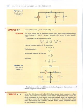
Let us apply what we have just learned to write the equations forthe network in Fig. 3.7 by EXAM PLE 3.2
inspection. Then given the following parameters, we will delennine the node voltages using
MATLAB: R, = R, = 2 kn, R, = R, = 4 kn, R, = I kn, iA = 4 mA, and ill = 2 rnA.
RJ ~••• Figure 3.7
Circuit used in Example 3.2.
•](https://image.slidesharecdn.com/basicengineeringcircuitanalysis9thirwin-160630150938/85/Basic-engineering-circuit-analysis-9th-irwin-123-320.jpg?cb=1719934140)
![104 CHAPTER 3 NODAL AND LOOP AN A LYS IS TECHNIQUES
•
SOLUTION The equations are
-v,(--'-) - v,(--'-)+ V3(--'- + --'- + --'-) = 0
R] R4 R] R4 Rj
which can also be written directly in matrix fOfm as
I I
-+ - 0
R, R, R,
[~J
I I I
[ -'A]0 -+-
fA ~ I nRJ R, R,
I I I
- + - + -
R, R, R, R, R,
Both the equations and the G matrix exhibit the symmetry that will always be present in cir-
cuits that contain only resistors and current sources.
Lf the component values are now used, the matrix equation becomes
I I
- +- 0
2k 2k 2k
[::] [- 0001I I I
0.0020 - + - =
4k 4k 4k
0
I I I
- +- + -
2k 4k 2k 4k Ik
or
[ 0.001 o - 0.0005 ] [ v,] [ - 0004]
-0.~005
0.0005 - 0.00025 v, = 0.002
- 0.00025 0.00175 V3 0
If we now employ these data with the MATLAB software, the computer screen containing
the data and the results of the MATLAB analysis is as shown next.
» G = [0 . 001 0 - 0.0005 ; 0 0.0005 -0 .00025;
- 0.0005 -0 . 00025 0 . 00175]
G =
0.0010 0 -0 .0005
0 0 . 0005 -0.0003
-0.0005 -0 .0003 0.0018
» I = [-0.004; 0.002; 0]
I =
-0.0040
0.0020
0
» V invCG)*l
V =
-4 . 3636
3.6364
-0.72 73](https://image.slidesharecdn.com/basicengineeringcircuitanalysis9thirwin-160630150938/85/Basic-engineering-circuit-analysis-9th-irwin-124-320.jpg?cb=1719934140)
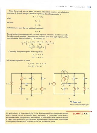
![SECTION 3 . 1
LearningAss ESS MEN IS
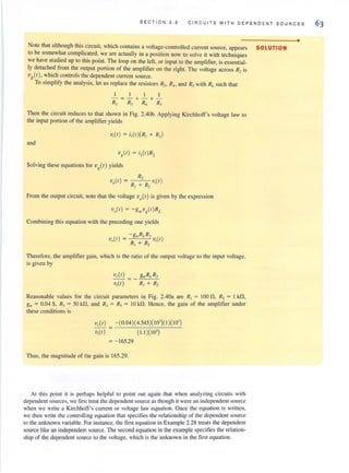
E3.1 Wr.ite the node equations for the circuit in Fig. E3.1.
V! V2
6 kfl 6 kfl
Figure E3.1
E3.2 Find all the node voltages in the network in Fig. E3.2 using MATLAB.
4mA t kfl I 2mA
Figure E3.2
NODA L ANALYSIS 105
ANSWER:
I I 10-3 ,- V,- - V,~4X
4k 12k
-I I 10-3•
12k V, + 4k V, = -2 X
ANSWER: V, = 5.4286 V,
V, = 2.000 V,
V3 = 3.1429 V.
CIRCUITS CONTAINING DEPENDENT CURRENT SOURCES The presence of a
dependent source may destroy the symmetrical form of the nodal equations that define the
circuit. Consider the circuit shown in Fig. 3.8, which contains a current-controlled current
source. The KCL equations for the nonreference nodes are
f3i + ~+ V ] - V2 = 0
o R] R2
and
where ;0 = V2/R3· Simplifying the equatjons, we obtain
(G, + G,)v, - (G, - ~G3)V2 = 0
or in matrix form
[
(G, + G,) - G, - ~G3)J [ v' ] = [0]- G, (G, + G,) v, 'A
ote thai the presence of the dependent source has destroyed the symmetrical nature of the
node equations.
~••• Figure 3.8
Circuit with a dependent
source.](https://image.slidesharecdn.com/basicengineeringcircuitanalysis9thirwin-160630150938/85/Basic-engineering-circuit-analysis-9th-irwin-125-320.jpg?cb=1719934140)
![SEC TION 3.1
Applying KCL at each of the nonreference nodes yields the equations
G, v, + G,(v, - v,) - iA = 0
iA + G,(v, - v,) + O<V, + G,(v, - v,) = 0
G,(v, - v,) + G,v, - iB = 0
where Vx = v2 - v3. Simplifying these equations. we obtain
(G, + G,)v, - G,v, = iA
Given the component values, the equations become
or
I I
-+-
Ik 2k k
1 I
- + 2 + -
k k 2k
0
[
0.0015
-0.001
o
2k
-0.001
2.0015
-0.0005
0
- (2+2Ik ) [V' ] [ 0002 ]v, = -0.002
1 1
v, 0.004
- + -
2k 4k
o ][V, ] [ 0.002 ]
- 2.0005 v, = - 0.002
0.00075 v, 0.004
The MATLAB input and output listings are shown next.
» G = [0 .0015 -0 . 001 0; -0.001 2.0015 -2. 0005;
o -0.0005 0.00075]
G =
0.0015 -0.0010 0
-0.0010 2.0015 - 2. 0005
0 -0 .0005 0 . 0008
» I [0.002; -0.002; 0.004]
I =
0.00 20
-0.00 20
0 .0040
» v inv(G)*1
V =
11.9940
15.9910
15.9940
NODAL ANALYSIS 107
•
SOLUTION](https://image.slidesharecdn.com/basicengineeringcircuitanalysis9thirwin-160630150938/85/Basic-engineering-circuit-analysis-9th-irwin-127-320.jpg?cb=1719934140)
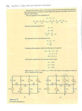
![•
108 CHA PTER 3 N O DAL A N D L OOP ANA LYSIS T E C H N IO U E S
LearningAssEsSMENTS
E3.3 Find the node voltages in the circuit in Fig. E3.3. ANSWER: V, = 16 V,
V, = - 8 V.
VI V2
10 kn
10 kn 10 kn
Figure E3.3
E3.4 Find the voltage Vo in the network in Fig. E3.4. ANSWER: Vo = 4 V.
Figure E3.4
V,
~----~~-r-~----~--~
+
3kn 12 kn 12 kn
CIRCUITS CONTAINING INDEPENDENT VOLTAGE SOURCES As is our practice,
in our discussion of this topic we will proceed from the simplest case to more complicated
cases. The simplest case is that in which an independent voltage source is connected to the
reference node. The following example illustrates this case.
EXAMPLE 3.5 Consider the circuit shown in Fig. 3.IIa. Let us determine all node voltages and branch currents.
•
SOLUTION This network has three nonreference nodes with labeled node voltages V" V" and V,. Based
on ourprevious discussions, we would assume that in orderto find aUthe node voltages we
would need to write a KCL equation at each of the nonreference nodes. The resulting three
linearly independent simultaneous equations would produce the unknown node Voltages.
However, note that VI and'V3 are known quantities because an independent vohage source is
connected directly between the nonreference node and each of these nodes. Therefore,
V, = 12 V and V, = -6 V. Furthermore, note that the current through the 9-kQ resistor is
[12 - (-6) ]/9k = 2 rnA from left to right. We do not know V, or the current in the remain-
iog resistors. However, since only one node voltage is unknown, a single-node equation will
produce it. Applying KCL to this center node yields
or
from which we obtain
V2 -V1 V2 - O V2 -V)
- -- + --+-- - = 0
12k 6k 12k
V,_ - 12 V"
.:.;",-'.=. + ..=. +
12k 6k
V, -<-6 ) =0
12k
[hint] 3
V, = - V
2
Any time an independent
voltage source isconnected
between the reference node
and a nonreference node, the
nonreference node voltage is
known.
Once all the node voltages are known, Ohm's law can be used to find the branch currents
shown in Fig. 3. I Ib. The diagram illustrates that KCL is satisfied at every node.
Note that the presence of the voltage sources in this example has simplified the analysis,
since two of the three linear independent equations are V, = 12 V and V, = -6 V. We will
find that as a general rule, whenever voltage sources are present between nodes, the node
voltage equations that describe the network will be simpler.](https://image.slidesharecdn.com/basicengineeringcircuitanalysis9thirwin-160630150938/85/Basic-engineering-circuit-analysis-9th-irwin-128-320.jpg?cb=1719934140)
![SECTION 3.2
VI
VS2
A + - B C
RI
:3 ~R4
+
vSI
8 R3 v4
R2 RS
F - v2 + E - Vs + D
Substituting these values into the two KVL equations produces the two simultaneous
equations required to determine the two loop currents; that is,
i,(R, + R, + R,) - i,(R,) = v"
-i,(R,) + i,(R, + R, + R,) = - vs>
or in matrix form
[
R' + R, + R, - R, J[i'J= [ vs, ]
-RJ R) + R~ + RS '2 - Vn
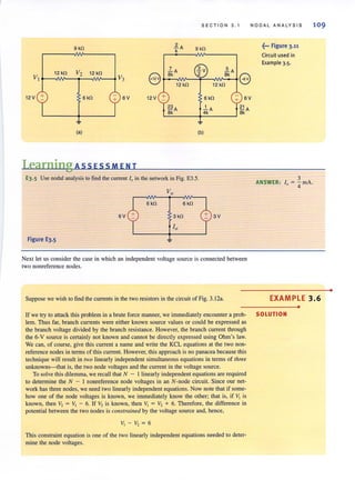
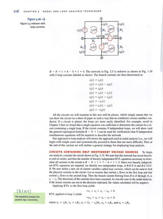
At this poinl. it is important to define what is called a mesh. A mesh is a special kind of loop
that does not contain any loops within it. Therefore, as we traverse the path of a mesh, we do not
encircle any circuit elements. For example, the network in Fig. 3. 19 containstwo meshes defined
by the paths A-B-E-F-A and B-C-D-E-B. The path A-B-C-D-E-F-A is a loop, but it is not a mesh.
Since the majority of our analysis in this section will involve writing KYL equations for meshes,
we will refer to the currents as mesh currents and the analysis as amesh analysis.
Consider the network in Fig. 3.20a. We wish to find the current I".
LOOP AN ALY S IS 117
~••• Figure 3.19
Atwo-loop circuit.
EXAMPLE 3.12
•
We will begin the analysis by writing mesh equations. Note that there are no + and - signs SOLUTION
on the resistors. However, they are not needed, since we will apply Ohm's law to each resis-
live element as we write the KYL equations. The equation for the first mesh is
-12 + 6k/, + 6k(!, - I,) = 0
The KYL equation for the second mesh is
6k(!, - I,) + 3k /, + 3 = 0
where Iv = II - 12"
Solving the two simultaneous equations yields I, = 5/ 4 rnA and I, = 1/ 2 rnA. Therefore,
10 = 3/ 4 rnA. All the voltages and currents in the network are shown in Fig. 3.20b. Recall
from nodal analysis that once the node voltages were determined, we could check our analy-
sis using KCL at the nodes. In this case, we koow the branch currents and can use KYL around
any closed path to check our results. For example, applying KYL to the outer loop yields
15 3
-12 + - + - + 3 = 0
2 2
0=0
Since we want to calculate the current 1(Jt we could use loop analysis. as shown in
Fig. 3.2Oc. Note that the loop current I, passes through the center leg of the network and,
therefore, I I = 10 , The two loop equations in this case are
-12 + 6k( /, + I,) + 6k/, = 0
and
-12 + 6k(I, + I,) + 3k/, + 3 = 0
Solving these equations yields I, = 3/ 4 rnA and I, = 1/2 rnA. Since the current in the
12-Y source is I, + I, = 5/ 4 rnA, these results agree with the mesh analysis.
•](https://image.slidesharecdn.com/basicengineeringcircuitanalysis9thirwin-160630150938/85/Basic-engineering-circuit-analysis-9th-irwin-137-320.jpg?cb=1719934140)
![118 CHAPTER 3 NODAL AND LOOP ANALYSIS TECHNIQUES
Figure 3.20 •••~
Circuits used in
Example 3.12.
Finally, for purposes of comparison, let us find I, using nodal analysis. The presence of
the two voltage sources would indicate that this is a viable approach. Applying KCL at the
top center node, we obtain
and hence.
and then
Vo - 12
6k
Vo Vo - 3
+-+--= 0
6k 3k
9
V = -y
, 2
V, 3
I, = 6k = 4rnA
Note that in this case we had to solve only one equation instead of two.
6 kfl
12V
3 kfl
6 kflr;::-.
~10
(a)
12V
3V
6 kfl 3 kfl
6 kfl 12
10
(e)
:!.!:!V ~V
+ 2 - Vo + 2 -
6 kfl
6 kfl
3 kfl
+
~mA
2
~mA -
4
(b)
3V
Once again we are compelled to note the symmetrical fann of the mesh equations that
describe the circuit in Fig. 3. 19. Note that the coefficient matrix for this circuit is symmetrical.
Since this symmetry is generally exhibited by networks containing resistors and independent
voltage sources, we can leam to write the mesh equations by inspection. In the first equation, the
coefficient of i! is the sum of the resistances through which mesh current I flows, and the coef·
ficient ofi2is the negative of the sum of the resistances common to mesh current I and mesh cur-
rent 2. The right·hand side of the equation is the algebraic sum of the voltage sources in
mesh I. The sign of the voltage source is positive if it aids the assumed direction of the current
tlow and negative if it opposes the assumed flow. The first equation is KYL for mesh I. In the
second equation, the coefficient of i2is the sum of all the resistances in mesh 2, the coefficient
ofi] is the negative of the sum of the resistances common to mesh I and mesh 2, and the right-
hand side of the equation is the algebraic sum of the voltage sources in mesh 2. In general, if we
assume all of the mesh currents to be in the same direction (clockwise or counterclockwise), then
if KYL is applied to mesh j with mesh current ij , the coefficient of ij is the slim of the resis-
tances in mesh) and the coefficients of the other mesh currents (e.g., ij-l , ij+ I) are the negatives
of the resistances common to these meshes and mesh j. The right-hand side of the equation is
equal to the algebraic sum of the voltage sources in meshj. These voltage sources have a posi·
tive sign if they aid the current flow ij and a negative sign if they oppose it.](https://image.slidesharecdn.com/basicengineeringcircuitanalysis9thirwin-160630150938/85/Basic-engineering-circuit-analysis-9th-irwin-138-320.jpg?cb=1719934140)
![SE CTION 3 . 2
Let us write the mesh equations by inspection for the network in Fig. 3.2 1. Then we will
use MATLAB to solve for the mesh currents.
The three linearly independent simultaneous equations are
(4k + 6k )/, - (0)/, - (6k)/, = -6
-(0)/, + (9k + 3k)/, - (3k)/, = 6
-(6k)/, - (3k)/, + (3k + 6k + 12k)/, = 0
or in matri x form
[
10k 0 -6kJ[/'J [ -6Jo 12k -3k I, = 6
-6k -3k 21k 13 0
Note the symmetrical form of the equations. The general form of the matrix equation is
RI = Y
and the solution of this matrix equation is
1= R- 'Y
The input/output data for a MATLAB solution are as follows:
» R = [10e3 0 -6e3; 0 12e3 - 3e3;
- 6e3 - 3e3 21e3]
R =
10000 0 -6000
0 12000 - 3000
-6000 -3000 21000
» V [ - 6; 6', 0 ]
V =
-6
6
0
» I = inv(R )*V
I =
1.0e - 003 *
- 0.6757
0.4685
- 0 . 1261
4 kn
8 6 kn
--06V
9kn
8 0; 12 kn
3 kn
CIRCUITS CONTAINING INDEPENDENT CURRENT SOURCES Just as the pres-
ence of a voltage source in a network simplitied the nodal analysis. the presence of a current
source simplifies a loop anal ysis. The following examples ill ustrate the point.
LOOP ANALYSIS 119
EXAMPLE 3.13
SOLUTION
~••• Figure 3.21
Circuit used in
Example 3.13.
•
•](https://image.slidesharecdn.com/basicengineeringcircuitanalysis9thirwin-160630150938/85/Basic-engineering-circuit-analysis-9th-irwin-139-320.jpg?cb=1719934140)
![•
120 CHAPTER 3 NODA L AND LO O P ANALYSIS TECHN I QUES
Learning ASS ESSM E N T
E3.8 Use mesh equations to find V, in the circuit in Fig. E3.8.
Figure E3.8
EXAMPLE 3.14
•
2 kO
6V
~~~--~~- +r--t-----
4kO
2 kO
6kO
+ 3V
Let liS find both V, and VI in the circuit in Fig. 3.22.
-<
+
33
ANSWER: V, = '5 v.
SOLUTION Although it appears that tbere are two unknown mesh currents, the current II goes directly
through the current source and, therefore, I. is constrained to be 2 rnA. Hence, only the
current h is unknown. KVL for the rightmost mesh is
2k(J, - II ) - 2 + 6k l, = 0
And, of course,
These equations can be written as
- 2k/l + 8k1, = 2
II = 2/ k
The input/output data for a MATLAB solution are as follows:
» R ; [-2000 8000; 1 0]
R ;
- 2000 8000
1 a
» V ; [2 ; 0.002]
V ;
2.0000
0.0020
» I ; in v( R) * V
I
0.0020
0.0008](https://image.slidesharecdn.com/basicengineeringcircuitanalysis9thirwin-160630150938/85/Basic-engineering-circuit-analysis-9th-irwin-140-320.jpg?cb=1719934140)
![» fo rmat long
» I
I =
0.00200000000000
0.00075000000000
SECTION 3 . 2
Note carefully that the firstsolution for hcontains a single digit in the last decimal place.
We are naturally led to question whethera number has been rounded off to this value. If we
type "format long," MATLAB will provide the answer using 15 digits. Thus, instead of
0.008, the more accurate answer is 0.0075. And hence,
9
V=6kI,=- Yo 2
To obtain ~ we apply KYL around any closed path. If we use the outer loop, the KYL
equation is
And therefore,
- v, + 4kI, - 2 + 6kI, = 0
21
V, = - Y
2
Note that since the current /[is known, the 4-kn resistor did not enter the equation in finding ~.
However, it appears in every loop containing the current source and, thus, is used in finding ~.
VI
2V
- + 0
4kO +
2mA
8 8 6 kO Vo
2 kO
~
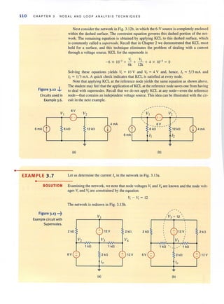
We wish to find Vo in the network in Fig. 3.23.
LOOP ANALYSIS
~... Figure 3.22
Circuit used in
Example 3.14.
121
EXAMPLE 3.15
•
Since the currents I, and I, pass directly through a current source, two of the three required SOLUTION
equations are
I, = 4 X 10-'
I, = - 2 X 10-'
The third equation is KVL forthe mesh containing the voltage source; that is,
4k(I, - I,) + 2k(I, - I,) + 6kl, - 3 = 0
These equations yield
I
I] = '4 mA
and hence,
-3
V = 6kl, - 3 = - Y
o 2
•](https://image.slidesharecdn.com/basicengineeringcircuitanalysis9thirwin-160630150938/85/Basic-engineering-circuit-analysis-9th-irwin-141-320.jpg?cb=1719934140)
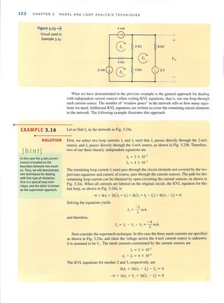
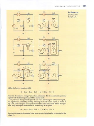
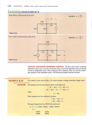
![S ECTION 3 . 2
» V = [0; 3]
V =
0
3
» I = inv (R)*V
I =
0 . 00150000000000
0.00150000000000
and therefore,
Vo = 6k1, = 9 V
For comparison, we will also solve the problem using nodal analysis. The presence of the
voltage sources indicates that this method could be simpler. Treating the 3-V source and its
connecting nodes as a supemode and writing the KCL equation for this supemode yields
_V-'.,_-_2V~l: Vl: Vl: + 3
+ -+ --=0
2k 4k 6k
where
These equations also yield Va = 9 V.
V, 3V
- +
2kfl +
2 V, ~ 4 kO 6kO Vo
12
~
Let us find Vo in the circuit in Fig. 3.26, which contains a voltage-controlled current source.
L OOP ANALYSIS
~••• Figure 3.25
Circuit used in
Example 3.17.
12 5
EXAMPLE 3 .18
•
The currents I, and I, are drawn through the current sources. Therefore, two of the equations SOLUTION
needed are
V,
I, = 2000
I, = 2 X 10-'
The KVL equation for the third mesh is
- 3 + 2k(i, - I,) + 6k/, = 0
where
V, = 4k (I, - I,)
Combining these equations yields
- I, + 21, = 0
I, = 2/ k
- 2k/, + SkI, = 3
•](https://image.slidesharecdn.com/basicengineeringcircuitanalysis9thirwin-160630150938/85/Basic-engineering-circuit-analysis-9th-irwin-145-320.jpg?cb=1719934140)
![•
126 CHAPTER 3 NODAL AND LOOP ANALYSIS TECHNIOUES
Figure 3.26 •••~
Circuit used in
Example 3.18.
The MATLAB solution for these equations is
» R ~ [- 1 2 0; 0 1 0; -2000 0 8000]
R ~
» V ~
V ~
» I ~
I ~
And hence,
-1
o
-200 0
[0 ;
2
1
o
0.002; 3]
o
o
8000
0
0.00200000000000
3.00000000000000
in v(R)*V
0.00400000000000
0.00200000000000
0 . 00137500000000
V. = 8.25 V
Vr
!J2000
V,- . +
4kn
~
2 kn
~
3V
0
+
6kn Vo
0
EXAMPLE 3.19 The network in Fig. 3.27 contains both a current-controlled voltage source and a voltage-
controlled current source. Let us use MATLAB to detennine the loop currents.
•
SOLUTION The equations for the loop currents shown in the figure are
where
4
I, = -
k
Vx
/ , = -
. 2k
-Iklx + 2k(!3 - I,) + Ik(i3 - I,) = 0
Ik(!, - 13) + Ik(!, - I,) + 12 = 0
Vx = 2k(!3 - I,)
I.t = 14 - /2](https://image.slidesharecdn.com/basicengineeringcircuitanalysis9thirwin-160630150938/85/Basic-engineering-circuit-analysis-9th-irwin-146-320.jpg?cb=1719934140)
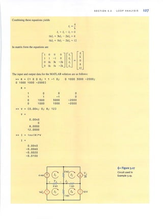
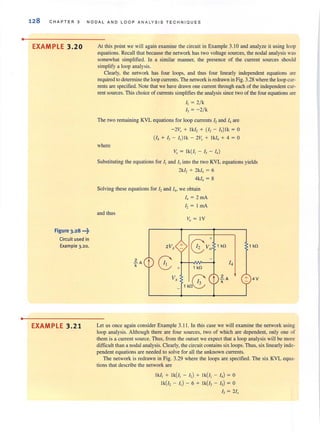
![SECTION 3 . 2
+ 1 kfl 1 kfl 6V
V,
8 8 C; I 21,
1 kfl 1 kfl 1 kfl
12 V 14 - I6
1 kfl
8 +2V,.
(;; 1k( ;
I, Io
- 12 + Ik( /, - I,) + 2V, = a
- 2V, + Ik( /, - I,) + Ik( /, - I,) = a
Ik(/, - I,) + Ik( /, - I,) + Ik/, = a
And the control variables for the two dependent sources are
It, = - Ik /,
I.r = Is - 10
Substituting the control parameters into the six KVL equations yields
3/, -h a - I, 0 a =a
- I, +212 a a - I, a =6/ k
a 0 13 a - 2/, +210 =a
- 3/, a a +14 0 a = 12/ k
21, - /2 a a +2/, - I. =a
a 0 a a -3/, +510 =a
which can be wriuen in matrix form as
3 - I a - I 0 0 I, a
- I 2 0 a - I a I, 6/ k
a a I a - 2 2 13 a
-3 a a a a I, 12/ k
2 - I a 0 2 - I I, a
0 a a a - 3 5 I, a
Although these six linearly independent simultaneous equations can be solved by any con-
veniem method, we will employ a MATLAB solution. As the following results indicate, the
current 10 is- 48 rnA.
» R = [3 -1 0 - 1 0 0 ; - 1 2 0 0 -1 0 ; 0 0 1 0 - 2 2 ;
-3 0 0 1 0 0 ; 2 - 1 0 0 2 -1 0 0 0 0 - 3 5]
R =
3 - 1 0 -1 0 0
-1 2 0 0 - 1 0
0 0 0 -2 2
-3 0 0 0 0
2 -1 0 0 2 -1
0 0 0 0 - 3 5
» V = [0; 0.006; O·, 0.012; 0; 0]
lO O P A N ALYSI S 12 9
f·· Figure 3.2 9
Circuit used in
Example 3.21-](https://image.slidesharecdn.com/basicengineeringcircuitanalysis9thirwin-160630150938/85/Basic-engineering-circuit-analysis-9th-irwin-149-320.jpg?cb=1719934140)
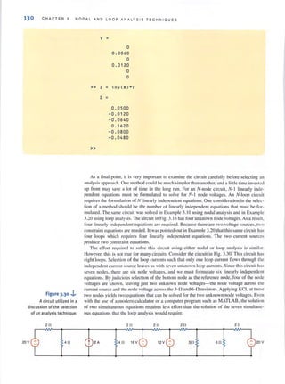
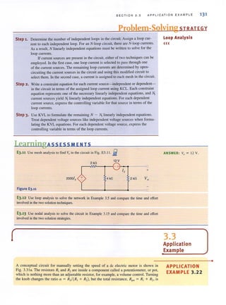
![132 CHAPTER 3 NODAL AND LOOP ANALYS IS TECHNIQUES
unchanged. In Ihis way Ihe pOI forms a vollage divider Ihat selS Ihe vollage V. . The
power amplifier OUIPUI, V", is four limes V""",. Power amplifiers can oUlpul Ihe hlg'h cur-
renls needed 10 drive Ihe molar. Finally, Ihe dc malar speed is proponional 10 V,,; Ihal is,
Ihe speed in rpm is some conslanl k times V. Withoul knowing Ihe delails of Ihe power
amplifier, can we analyze Ihis syslem? In parlicular, can we develop a relalionship belween
rpm and ex?
Figure 3.31 ..-~
(a) A simple de motor
driver and (b) the circuit
model used to analyze it.
5V
1 rIR
pot
R2
~. = 1
_ 1·=0 +
Vspeed
Power
amp
VMiVspeed = 4
+
VM
I
de
motor
•
-
- 5:
(a)
5V
(b)
.l.
Power amp
model
+
4Vspeed
~
,
-- - - - -- - ---
-
1
SOLUTION Since the power amplifier output voltage is proponional to its input, we can model the
amplifier as a simple dependent source. The resulting circuit diagram is shown in
Fig. 3.31 b. Now we can easily develop a relationship between motor speed and the pot posi-
tion, ex. The equations that govern the operation of the motor, power amplifier, and the volt-
age divider are
speed (rpm) = KM V"
VM = 4Yspccd
v. = 5 R, 5[ R, ] = 5a
.",d R, + R, = R"",
R, = aR"", R, = (I - a)R"",
Combining these relationships to eliminate v.""" yields a relationship between motor speed
and a, that is, rpm = 20a. If, for example, the motor constant K" is 50 rpm/ V, then
rpm = IOOOa
This relationship specifies that the motor speed is proponional to the pot knob position.
Since the maximum value of ex is I, the motor speed ranges from °to 1000 rpm.
Note that in our model, the power amplifier, modeled by the dependent source, can
deliver allY current the motor requires. Of course, this is not possible, but it does demon-
strate some of the tradeoffs we experience in modeling. By choosing a simple model, we
were able to develop the required relationship quickly. However, other characteristics of an
actual power amplifier have been omitted in this model.](https://image.slidesharecdn.com/basicengineeringcircuitanalysis9thirwin-160630150938/85/Basic-engineering-circuit-analysis-9th-irwin-152-320.jpg?cb=1719934140)
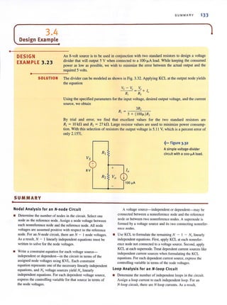
![o 3.6
0 3.5 Usc nodal analysis to find both VI and V{} in the circuit ill
Fig. P3.S.
i
2 mA
VI V2
6kO 2 kO
12 mA 3kO 6 kO 1 kO
Figure P3.5
PROBLEM S 135
G
+
Vo
0
Write the node equntions for the circuit in Fig. P3.6 in
matrix form, and rind all the node voltages lIsing
MATLAB.
3.8 Find III in the circuit in Fig. P3.8 using nodal anal ysis.
8 kll
3 mA
.------{- } ----, 2 kll
1 mA t1kO V2 3kll
VI ~--~~~~~~--~ V3
3 kll
6 kll
2kO 6 mA 4 kll
Figure p).8
Figure p).6
o
~ 3.7 Find Y" in the network in Fig. P3.7. 3·9 Use nodal analysis 10 lind I" in the network in Fig. P3.9. 0
2 rnA
4 mA 2 kll
4 rnA
t 4 k[J
1 k[J 1 kO +
1 k[J t 1 rnA 2 k[J
2 kf]
4 kO
6 rnA
t 12 kO
10
Figure P).7
Figure P).9](https://image.slidesharecdn.com/basicengineeringcircuitanalysis9thirwin-160630150938/85/Basic-engineering-circuit-analysis-9th-irwin-155-320.jpg?cb=1719934140)
![i 3.18 Find ~Q in the network in Fig. P3. IS using nodal
equations.
1 kfl
2 mA
1 kfl
-
6V + 1 kfl 1 kfl
+
Va
L-------~--____~_____~o
Figure 1'].18
3.19 Find 10 in the network in Fig. P3. 19 using nodal analysis.
4 kfl
3 kfl
2 mA
12 V 6 kfl 2 kfl
Figure 1'].19
3.20 Use nodal analysis to find 10 in the circuit in Fig. P3.20.
2 kfl
2 mA 4 mA
12 V 2 kfl 2 kfl
Figure 1'].20
3.21 Find Vo in the circuit in Fig. P3.21 using nodal analysis.
6 mA
12 kfl
- r-------vVv---,
6 kfl
4 mA
+
12 V + 9V
Figure 1'].21
PROBLEMS 137
3.22 Use nodal analysis to find Vo in the network in
Fig. P3.22.
1 kfl 2 kfl 1 kfl
2kfl 1 kfl
12 V + t 2mA 1 kfl
Figure 1'].22
+
VO
3.23 Find 10in the circuit in Fig. P3.23 using nodal analysis.
6kfl
6V
6 kfl
+
6 kfl 12 kfl 12 kfl 6 kfl
Figure 1'].23
3.24 Usc nodal analysis to find If) in the circuit in Fig. P3.24.
3V
6V
r-~~--~~-+r-~--~~-.
6kfl 12 kfl
12 kfl 6 kfl
Figure 1'].24
3.25 Using nodal analysis, find 1;, in the network in
Fig. P3.25.
3V
r-----~+-~----,
4 kfl 2 kfl
~--~~-4r-~~--~-------o
+
6V 2mA 6 kfl
Figure 1'].25
3V](https://image.slidesharecdn.com/basicengineeringcircuitanalysis9thirwin-160630150938/85/Basic-engineering-circuit-analysis-9th-irwin-157-320.jpg?cb=1719934140)
![142 CHAPTER 3 NODAL AND L OOP ANAL Y SIS TE CHNIQUES
i 3.58 Find~) in the circuit in Fig. P3.58 using mesh
analysIs.
6 kn
2kn
12V +
Figure 1'3.58
3kn
---0
+
~ 8mA
3.59 Usc mesh analysis to find Vo in the circuit in Fig. P3.59.
2 kn
6V 4 kn
4kn
+ Vo
8 kn
8 kn
3.62 Use loop analysis to calculate Ihe power supplied by the
20-V voltage source in the circuit in Fig. P3.62.
sn
sn lOn
20n + 20V
Figure 1'3.62
3.63 Find /" in the network in Fig. P3.63 using loop analysis.
1 kn
1 kn
12V
t----I'./II'-- t---{+ -
1 kn
1 kn t 6mA
Figure 1'3.59 Figure 1'3.63
3.64 Use loop analysis to find It] and I, in the network in
3.60 Usc mesh analysis 10 find I" in the network in Fig. P3.60. Fig. P3.64.
3 kn
12V
-+~~--~~--~--~~-,
3kn 2 kn
2 kn
Figure 1'3.60
1 kn
o 3.61 Use loop analysis to find Vo in the circuit in Fig. P3.61.
1 kn
6V
-+
1 kn 2kn
0
+
1 kn
2 mA
t 1 kn VO
12V +
0
Figure 1'3.61
6 kn
3 kn
12 mA 4 kn + 12V 2 kn
10 I,
L -____~----~----~
Figure 1'3.64
3.65 Find /0 in the network in Fig. P3.65 using loop analysis.
Then solve the problem using MATLAB and compare
your answers.
6 kn
6kn 6kn
BV
Figure 1'3.65](https://image.slidesharecdn.com/basicengineeringcircuitanalysis9thirwin-160630150938/85/Basic-engineering-circuit-analysis-9th-irwin-162-320.jpg?cb=1719934140)

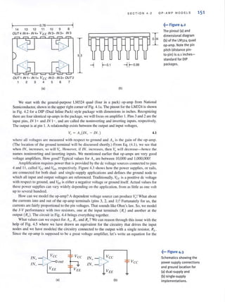
![15 2 C HAPTER 4 OPERATIONAL AMPLIFIER S
Figure 4.4 •••~.
A simple model for the gain
characteristics of an op-amp.
+ +
Vi,,(r)
Ro +
Ri
Figure 4.5 ...~
A network that depicts an
op-amp circuit. Vsand RThI
model the driving circuit, while
the load is modeled by R,. The
circuit in Fig. 4.4 is the
op·amp model.
1N+(r) + vo(r)
+ A oVin
IN_(r)
+
+
Vs +
overall gain of the circuit Vj Vs. Using voltage division at the input and again at the output,
we quickly produce the expression
v, [ Ri ] [ RL ]
Vs = R; + R Th l Ao Ro + RL
To maximize the gain regardless of the values of Rnll and R L l we make the voltage divi-
sion ratios as close to unity as possible. The ideal scenario requires that Ao be infinity, R; be
infinity, and Robe zero, yielding a large overall gain of AI)' Table 4. I shows the actual values
of AQ • Ri • and R, for a sampling of commercial op-amps intended for very different applica-
tions. While A01 R;, and RQ are not ideal, they do have the correct tendencies.
The power supplies affect perfommnce in two ways. First. each op-amp has minimum and
maximum supply ranges over which the op-amp is guaranteed to function. Second. for proper
opemtion, the input and output voltages are limited to no more than the supply voltages.* If the
inputs/output can reach within a few dozen millivolts of the supplies. then the inputs/
output are called rail-to-rail. Otherwise. the inputs/output voltage limits are more severe-
usually a volt or so away from the supply values. Combining the model in Fig. 4.4, the values
in Table 4.1, and these VO limitations, we can produce the graph in Fig. 4.6 showing the
output-input relalion for each op-amp in Table 4.1. From the graph we see that LMC6492 and
MAX424D have rail-Io-rail outputs while the LM324 and PAD3 do not.
TABLE 4.1 A list of commercial op-amps and their model values
MANUFACTURER COMMENTS
National LM324 100,000 1.0 20 General purpose, up to 1: 16 V
supplies, very inexpensive
National LMC6492 50,000 10' 150 low voltage, rail·to·rail inputs
and outputs'
Maxim MAX4240 20,000 45 160 Micro·power (1.8 V supply
@ 10 ~), rail-to·rail inputs
and outputs
Apex PA03 125,000 10' 2 High-voltage, ± 75 V and high·
output current capability, 30 A.
That's 2 kW!
tRail-to-rail is a trademark of Motorola Corporation. This feature isdiscussed funher in the following paragraphs.
* Op-amps arc available that have input and/or output voltage ranges beyond the supply rails. However. these devices
constitute a very sTllall perccnt:lge of the op-amp market and will lIot be discussed here.](https://image.slidesharecdn.com/basicengineeringcircuitanalysis9thirwin-160630150938/85/Basic-engineering-circuit-analysis-9th-irwin-172-320.jpg?cb=1719934140)
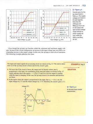
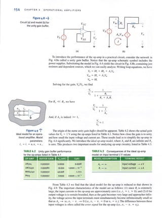
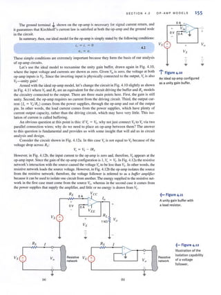
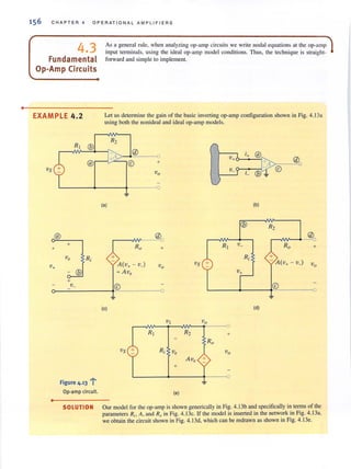
![SECTION 4.3 FUNDAMENTAL OP·AMP CIRCUITS
The node equations for the network are
_V,--I _- _V-,,-S V I VI - Vo
+ - + = 0
RI Ri R2
V I} - VI v" - A Ve
--"--::-----'- + = 0
R2 Ro
where vt' = -VI . The equations can be written in matrix form as
Solving for the node voltages, we obtain
[
, ,
[
VI ] = -'- R, + Ro
Vo ~ I A
- - -
Rz Ro
where
( I I 1 )( 1 I ) ( 1 )( ' A)~ - -+ - +- - + - - - - - -
RI Ri Rz Rz Ro Rz Rz Ro
Hence,
which can be written as
If we now employ typical values for the circuit parameters (e.g., A = 10', Ri = 10' n ,
Ro = 10 n , RI = I kn, and R, = 5 kn), the voltage gain of the network is
V"
- = -4.9996994 '" -5.000
Vs
However. the ideal op-arnp has infinite gain. Therefore. if we take the limit of the gain equa-
tion as A ~ 00, we obtain
(
Vo) R,lim - = - - = - 5.000
A- co Vs RI
Note that the ideal op-amp yielded a result accurate to within four significant digits of that
obtained from an exact solution of a typical op-amp model. These results are easily repeated
for the vast array of useful op-amp circuits.
We now analyze the network in Fig. 4.13a using the ideal op-amp model. [n this model
i+ = L :=; a
V+ = v_
157](https://image.slidesharecdn.com/basicengineeringcircuitanalysis9thirwin-160630150938/85/Basic-engineering-circuit-analysis-9th-irwin-177-320.jpg?cb=1719934140)
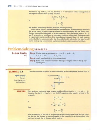
![SECTION 4.3 FUN DAME N TAL OP-AMP CIRCUITS 159
The remaining examples, though slightl y more complicated, are analyzed in exactly the
same manner as those outlined above.
Gain error in an amplifier is defined as
_ [actual gain - ideal gain]
GE - 'd I . x 100%
1 ea gam
We wish 10 show thaI for a standard noninverting contiguration with finite gain Au, the gain
error is
where Il = R,/ (R, + R, ).
_-_1:..:0..:.0.:..:%:-GE =.,-
I + A"I'
The standard noninverting configuration and its equi valent circuit are shown in Fig. 4. 15a
and b, respectively. The circuit equations for the network in Fig. 4.1Sb are
v"v· =- and
In An
The expression that relates the input and output is
~nd thus rhe actual gain is
Recall that the ideal gain for this circuit is (R, + R,)IR,
error is
[
A" I]GE = I + A,,1l Il 100%
1m
which when simplified yields
GE =
Vs 0-----1'"
>--.- ovo
-100%
I + A"j3
1/ 1l. Therefore, the gain
Vj t-- -IM------'
R2 R2
(al (bl
EXAMPLE 4.4
•
SOLUTION
~". Figure 4,15
Circuits used in Example 4.4.
•](https://image.slidesharecdn.com/basicengineeringcircuitanalysis9thirwin-160630150938/85/Basic-engineering-circuit-analysis-9th-irwin-179-320.jpg?cb=1719934140)
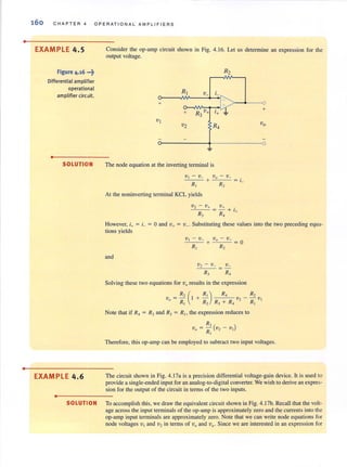
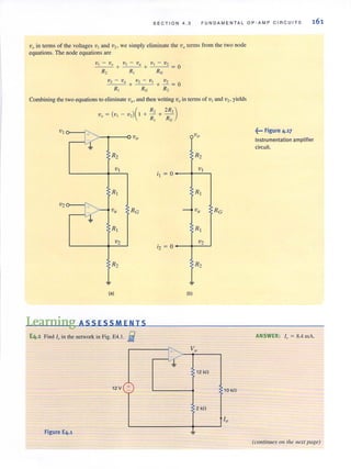
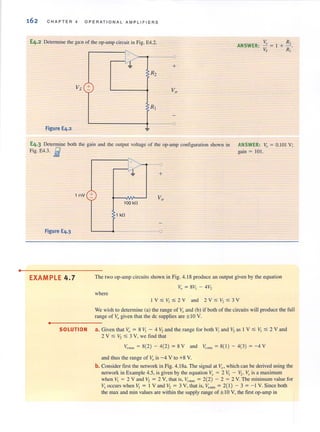
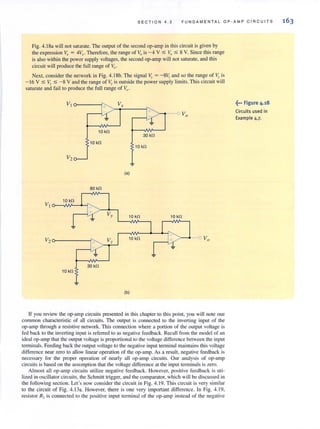
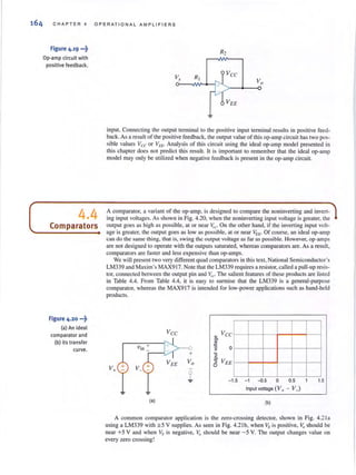
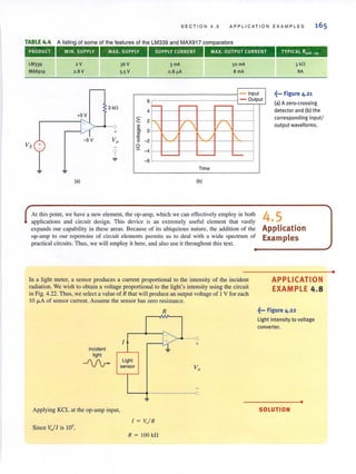
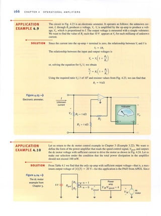
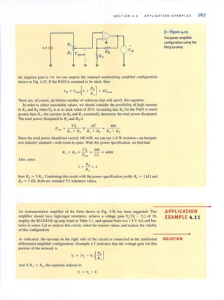
![168 CHAP TER 4 OP ERATION AL AMPLIFIERS
Figure 4.26 •••~
An instrumentation
amplifier using the
MAX4240 op·amp.
Differential amplifier
3V ------------ -- ------~
V, RA 3V
+
VI
+
R8 = RA Vo-~
3V A
~-
1
RI
R
1.5 V ~
R2
l B
1.5V 1 RA R8 = RA
+ , ,,,
V2
,
~
_______ ____________ J
- ~
If we can find a relationship between VI I V2 , and '-':r and ~" then an expression for the over-
all vohage can be wrillen. Applying KCL al node A yields
VI - V2 Vx - VI
- --
R R,
or
v, = V,[I+ :, ] - V,[:']
In a similar manner. ar node B we obtain
VI -V2
V2- Vy
R R,
or
By combining these equations, the output voltage can be expressed as
Vo= V, - V, = V,[I + : ,] - V,[:'] + V,[:' ]- +
If the resislOrs are selecled such that R, = R" then the vohage gain is
Vo---= I
V, - V,
2 R,
+ -
R
R,]+-
R
For a gain of +I0, we set R] = 4.5 R. To maintain low power, we will use fairly large values
for these resistors. We somewhat arbitrarily choose R = 100 kfl and R, = R, = 450 kfl. We
can use 100 k!1 resistors in the differential amplifier stage as well.
Note that the voltage gain of the instrumentation amplifier is essentially the same as
that of a generic differential amplifier. So why add the cost of two more op-amps? In this
configuration the inputs "l and V2 are directly connected to op-amp input terminals; there-
fore, the input resistance of the intrumentation amplifier is extremely large. From
Table 4.1 we see that R ill for the MAX4240 is 45 MO. This is not the case in the tradi-
tional differential amplifier where the external resistor can significantly decrease the
input resistance.](https://image.slidesharecdn.com/basicengineeringcircuitanalysis9thirwin-160630150938/85/Basic-engineering-circuit-analysis-9th-irwin-188-320.jpg?cb=1719934140)
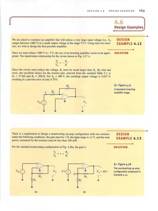
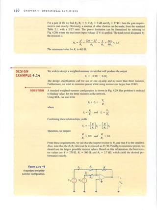
![SECTION 4 . 6 DESIGN EXAMPLES 171
In Example 2.36, a 250-0. resistor was used to convert a current in the 4- to 20-mA range
to a voltage such that a 20-mA input produced a 5-V output. In this case, the minimum cur-
rent (4 mAl produces a resistor voltage of I V. Unfortunately, many control systems oper-
ate on a 0- to 5-V range rather than a 1- to 5-V range. Let us design a new converter that will
output 0 V at 4 rnA and 5 V at 20 mAo
The simple resistor circuit we designed in Example 2.36 is a good start. However, the
voltage span is only 4 V rather than the required 5 V, and the minimum value is not zero.
These facts imply that a new resistor value is needed and the output voltage should be
shifted down so that the minimum is zero. We begin by computing the necessary resistor
value.
R = Vmax - Vmin
Imax - Imin
5 - 0
- -=-----=-- = 312.5 fl
0.02 - 0.004
The resistor voltage will now range from (0.004)(312.5) to (0.02)(312.5) or 1.25 to 6.25 V.
We must now design a circuit that shifts these voltage levels so that the range is 0 to 5 Y.
One possible option for the level shifter circuit is the differential amplifier shown in Fig.
4.30. Recall that the output voltage of this device is
R,
Vo = (V, - V"",,) R;
Since we have already chosen R for a voltage span of 5 V, the gain of the amplifier should
be I (i.e., R, = R,). Clearly, the value of the required shift voltage is 1.25 V. However, we
can verify this value by inserting the minimum values into this last equation
and find
R,
0= [(312.5)(0.004) - V'hlf,] ~
R,
V,hlf, = (3 12.5)(0.004) = 1.25 V
There is one caveat to this design. We don't want the converter resistor. R, to affect
the differential amplifier, or vice versa. This means that the vast majority of the
4-20 mA current should flow entirely through R and not through the differential ampli-
fier resistors. If we choose R1 and R2 » R, this requirement will be met. Therefore,
we might select R, = R, = 100 kfl so that their resistance values are more than 300
times that of R.
4-20 mA t
Differential amplifier with shiller
r------------- ---- -----
I R J
:
, ,
+ ',
,
,
R V, :
,
+
DESIGN
EXAMPLE 4.15
•
SOLUTION
f- figure 4.30
A 4-20 mA to 0-5 V
converter circuit.
•](https://image.slidesharecdn.com/basicengineeringcircuitanalysis9thirwin-160630150938/85/Basic-engineering-circuit-analysis-9th-irwin-191-320.jpg?cb=1719934140)
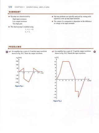
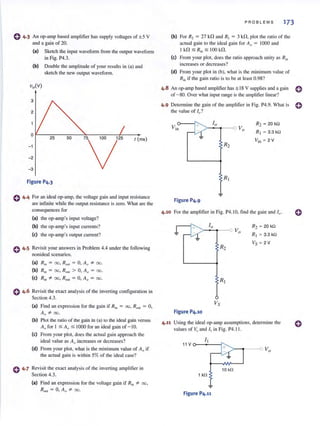
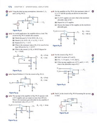
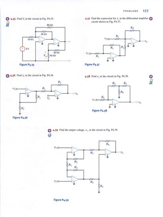
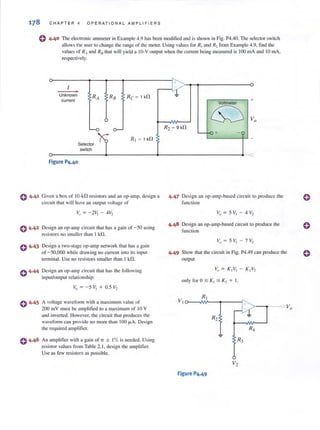
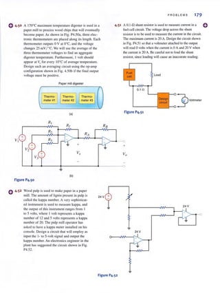
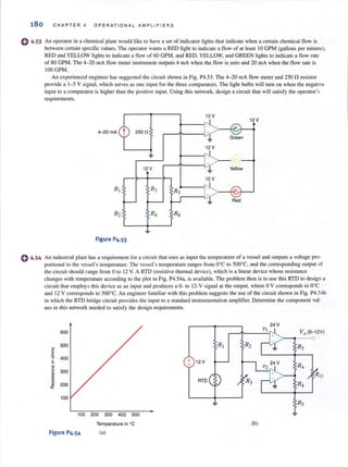
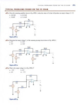
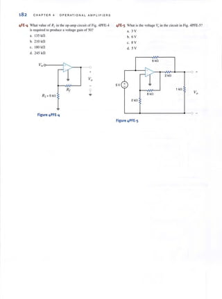
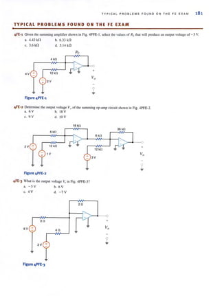
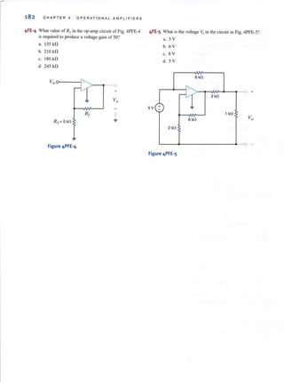

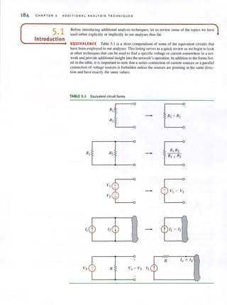
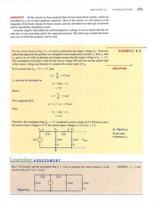
![o
186 C HAPTER 5 ADDITIONAL ANALYSIS TE CHNIQUES
( 5.2
__S_u.:..p_e...;rp:...o_s_i_ti_o_",
EXAMPLE 5.2 To provide motivation for this subject, let us examine the simple circuit of Fig. 5.2a in which
two sources contribute to the current in the network. The actual values of the sources are left
unspecified so that we can examine the concept of superposition.
..0-------
SOLUTION The mesh equations for this network are
Figure 5-2 J..
Circuits used to illustrate
superposition.
6ki,(I) - 3ki,(I) = V,(I)
-3ki, (I) + 9ki,(I) = - V,(I)
Solving these equations for it(l) yields
. V,(I) V,(I)
1(1) - - - -, - 5k 15k
In other words, the current il(l) has a component due to VI(I) and a component due to V2(1). In
view of the fact that il(I) has two components, one due to ""ch independent source, it would be
interesting to examine what each source acting alone would contribute to iI(1). For VI(1) to act
alone, V,(I) must be zero. As we pointed out in Chapter 2, vAl) = 0 means that the source V,(I )
is replaced with a short circuit. Therefore, to determine the-value of il (l) due to VI(I) only,-we
employ the circuit in Fig. S.2b and referto this value of il(I) as il(l).
., 'V,( I ) V,( I )
1,(1) = (3k)(6k) 5k
3k +
3k
+
6k
Let us now determine the value of il (l) due to V2(1) acting alone and refer to this value as
i;(I ). Using the network in Fig. 5.2c,
...( )'2 f =
v,(I )
(3k)(3k)
6k +
3k
+
3k
Then, using current division, we obtain
-2v,(I)
15k
... - 2v,(I) ( 3k ) - V,(I )
1,(1) = 15k 3k + 3k = 15k
Now, iF we add the values of i;(I) and i;'(I ), we oblain Ihe value computed directly; thai is,
.() "()+'''() V,(I) V,( I )
'I t = ' I t '] I = 5k - 15k
Note that we have superposed the value of ij (t) on ii'(') , or vice versa, to determine the
unknown current
3 kO 6 kO i,(I) 3kO 6kO i'i(l) 3 kO 6 kO i2(1)
V2(1)V2(1) VI (I)
3kn
8 3 kO 3kO
(a) (b) (c)
1](https://image.slidesharecdn.com/basicengineeringcircuitanalysis9thirwin-160630150938/85/Basic-engineering-circuit-analysis-9th-irwin-208-320.jpg?cb=1719934140)
![SECT I ON 5 . 2
What we have demonstrated in Example 5.2 is true in general for linear circuits and is a
direct result of the property of linearity. The principle of supeqJOSilion, which provides us
with this ability to reduce a complicated problem to several easier problems-each contain-
ing only a single independent source-states that
In any linear circuit containing multiple independent sources, the current or voltage at any
point in the network may be calculated as the algebraic sum of the individual contributions of
each source acting alone.
When determining the contribution due to an independent source, any remaining voltage
sources are made zero by replacing them with short circuits, and any remaining current sources
are made zero by replacing them with open circuits.
Although superposition can be used in linear networks containing dependeJ1l sources, it is
not useful in this case since the dependent source is never made zero.
As the previous example indicates, superposition provides some insight in determining the
contribution of each source to the variable under investigation.
We will now demonstrate superposition with two examples and then provide a problem-
solving strategy for the usc of this technique. For purposes of comparison. wc will also solve
the networks using both node and loop analyses. Furthermore, we will employ these same
networks when demonstrating subsequent techniques, if applicable.
Let us use superposition to find Vo in the circuit in Fig. 5.3a.
-+ 0
2 kfl + 2 k!l
103V
1 kfl 2mA 6 k!l Va 1 kfl 6 kfl
0
(a) (b)
2k!l 3V
+ 0 -+
2 kfl +
3V
1 kfl 6 kfl V"a 1 kfl r}] 12 6 kfl
0
(c) (d)
The contribution of the 2-mA source to the output voltage is found from the network in
Fig. 5.3b, using currenl division
and
I - (2 x 10⁻³)( Ik + 2k )
" - Ik + 2k + 6k
2
= - rnA
3
V; ~ 1,,(6k) ~ 4 V
The contribution of the 3-V source to the output voltage is found from the circuit in
Fig. 5.3c. Using voltage division,
Therefore,
V; ~ 3Ck + ~~ + 6k)
~ 2V
Vo = V~ + V~ = 6 V
Although we used two separate circuits to solve the problem, both were very simple.
SUPERPOSITION
•
EXAMPLE 5.3
+
V'0
+
Va
~... Figure 5.3
Circuits used
0 in Example 5.3.
•
SOLUTION](https://image.slidesharecdn.com/basicengineeringcircuitanalysis9thirwin-160630150938/85/Basic-engineering-circuit-analysis-9th-irwin-209-320.jpg?cb=1719934140)
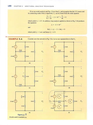
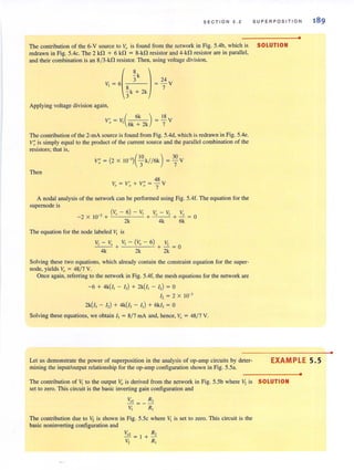
![190 C HAPTER 5 ADDITIONAL ANALYSIS TE CHN I OUES
Figure 5.5 •••~
(a) a superposition
example circuit; (b) the
circuit with V2 set to zero;
(c) the circuit with V, set
to zero.
Therefore, using superposition,
V, = [t+ ~:]v, - [~:]VI
Thus, in this case, we have used what we learned in Chapter 4, via superposition, to imme-
diately derive the inpuuoutput relationship for the network in Fig. 5.5a.
R2
+
VI Va'
R2
~ ~ i
~ (b)
+
R2
V, + V2 Vo
i +
(a) V2 + R2 Vo2
R,
~ ~ i
(e)
Problem-Solving STRATEGY
Applying
Superposition
»)
Step 1. In a network containing multiple independent sources, each source can be
applied independently with the remaining sources turned off.
Step 2. To tum off a voltage source, replace it with a short circuit, and to turn off a
current SOUTce, replace it with an open circuit.
Step 3. When the individual sources are applied to the circuit, all the circuit laws
and techniques we have learned, or will soon learn, can be applied to obtain a
solution.
Step 4. The results obtained by applying each source independently are then added
together algebraically to obtain a solution.
Superposition can be applied to a circuit with any number ofdependent and independent sources.
In fact, superposition can be applied to such a network in a variety of ways. For example, a
circuit with three independent sources can be solved using each source acting alone, as we
have just demonstrated. or we could use two al a time and sum the result with thal obtained
from the third acting alone. In addition, the independent sources do not have to assume their
actual value or zero. However, it is mandatory that the sum of the different values chosen add
to the total value of the source.](https://image.slidesharecdn.com/basicengineeringcircuitanalysis9thirwin-160630150938/85/Basic-engineering-circuit-analysis-9th-irwin-212-320.jpg?cb=1719934140)
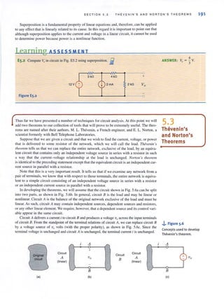
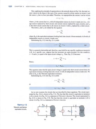
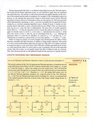
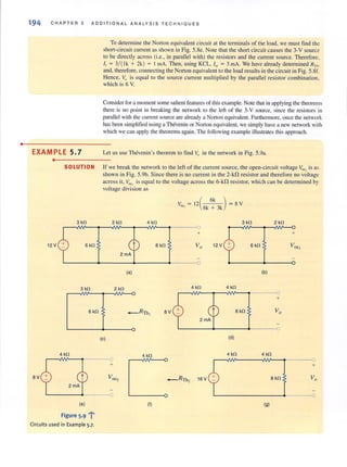
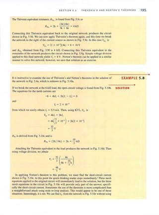
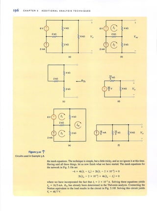
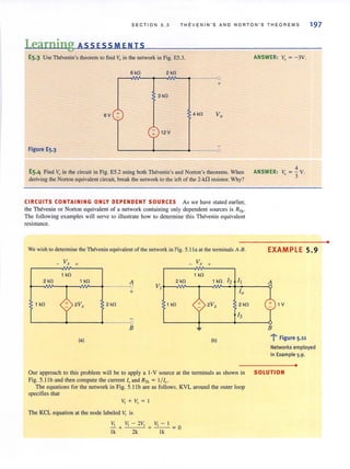
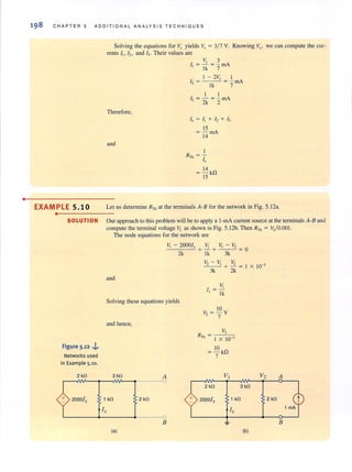
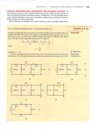
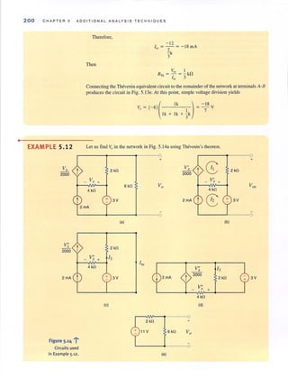
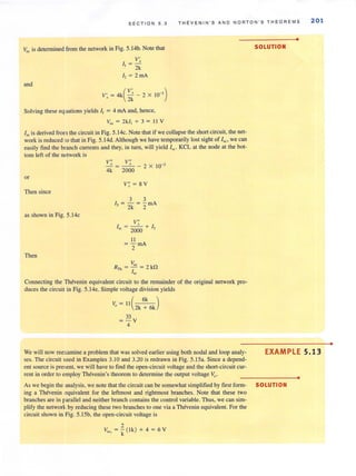
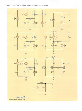
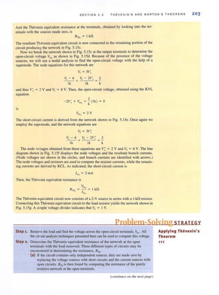
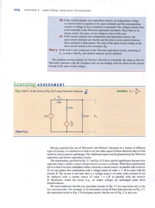
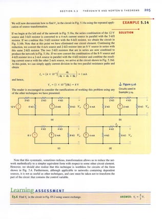
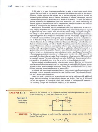
![SECTION 5.3 THEVEN IN ' S AND NORTON'S THE OREMS 207
where R, and R,. are in kn. Superposition can be used effectively to find Voc' If the 12-V
source is replaced by a shon circuit
[
Rx ]V --6 - -
oc! - R,T+ 4
Applying this same procedure for the 6-V source yields
V"" ~ 12
and the total open-circuit voltage is
Voc ~ 12 - 6[~]Rx + 4
5,8
In EXCEL we wish to (I) vary Rx between 0 and IO kn, (2) calculate RTh and Voc at each
R,r value, and (3) plot Voc and RTh versus Rx. We begin by opening EXCEL and entering col-
umn headings m;shown in Fig. 5.18a. Next, we enter a zero in the first cell of the Rxcolumn
at column-row locationA4, To automatically fill the column with values, go to the Edit menu
and select Fill/S~ries to open the window shown in Fig. 5.18b, which has already been edited
appropriately for IOI data points. The result is a series of R, values from 0 to 10 kn in 100 n
steps. To enter f<j. (5.8), go to location B4 (right under the Voc heading). Enter the foUowing
text and do not forget the equal sign:
;12-6*A4 / (A4+4)
This is Eq, (5.8) with R,Treplaced by the first value for Rxo which is at column-row location
A4. Similarly for R.n., enter the following expression at C4.
Type
..i,. Figure 5.18
(a) The EXCEL spreadsheet
for Example 5.15 showing
the desired column
headings. (b) The
Fill/Series window edited
for varying R, and (c) the
final plot of V" and RTh•
0.<. ""
® L.ne« • Ooy
(a)
O !:i'owth Weekday
O Qote '''''''h
oD'end O A<toEiI 'tear
;teo ......., t.::lo.:!!t[_ ...J StQP ......., 1t.:1:,:.o_-1
OK I I c""'~
15
12.5
10
~
7.5u
::,.0
5
2.5
, 7-
/
/:j
o
o 2.5
(b)
3
--~
./
~
2.5
2
a
1.5 ~
I: Voc,C- R1l1 0.5
7.5
R (kn)
(e)
5
o
10
<>:](https://image.slidesharecdn.com/basicengineeringcircuitanalysis9thirwin-160630150938/85/Basic-engineering-circuit-analysis-9th-irwin-229-320.jpg?cb=1719934140)
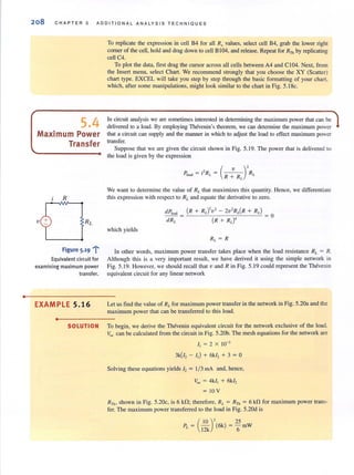
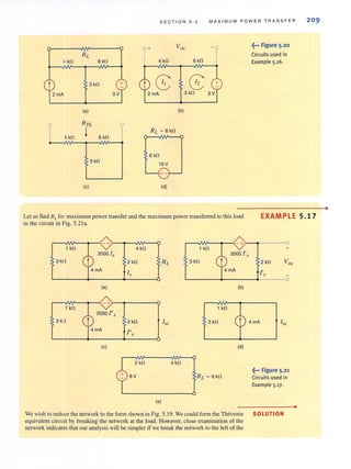
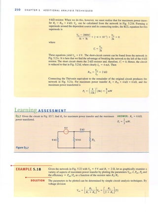
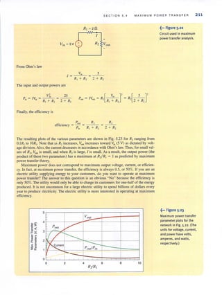
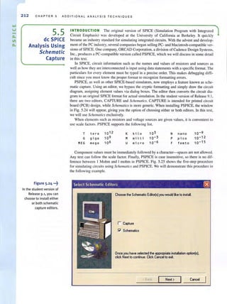
![S E CT I ON 5 .5 DC SPICE ANALYSIS USING SCHEMATIC CAPTURE 213
STEP 1 Draw the Circuit STEP 2 Change Names and Values
(a) Get parts
+ (a) Name parts
(b) Arrange parts (b) Set parts vatues
(c) Wim parts (c) Name nodes
(d) Auxiliary parts such as
VIEWPOINT
..STEP 3 Save the File
STEP S Output the Results
..(a) Vie"" edit, and print
the output lile STEP 4 Simulate the Circuit
(b) Print the schematic
1+(c) Copy the schematic to (a) Set the analysis type
othm programs (b) Simulate the circuil
V2
6V
+-
Ra Rc
VI
2 kO 2 kO
Rb
+ I I
t 2 V + 3kO Va t 4 rnA
-
10 -
~--- Figure 5.25
The five·step procedure for
PSPICE simulations.
i---Figure 5_26
Ade circuit used for
simulation.
ice Scheonaties . [Schoonatiel p.l 1 G]f51(8)
A de SIMULA -ION EXAMPLE The followi ng font conventions will be used throughout
this tutorial. Uppercase text refers to PSPICE programs, menus, dialog boxes, and utilities.
All boldface text denotes keyboard or mouse inputs. In each instance, the case in boldface
text matches that in PSPICE. Let us simulate the circuit in Fig. 5.26 using PSPICE.
Following the tl wchart procedure in Fig. 5.25, the first step isto open Schematics using the
SlartIProgram,,/Pspice SludenUSchematics sequence of pop-up menus. When Scizemalics
opens, our screen will change to the Schematics editor window shown in Fig. 5.27.
_ er X
'1' Figure 5.2 7
The Schematics editor
window.](https://image.slidesharecdn.com/basicengineeringcircuitanalysis9thirwin-160630150938/85/Basic-engineering-circuit-analysis-9th-irwin-235-320.jpg?cb=1719934140)

![S ECTION 5 . 5
Part BroJ/ser Basic,
PartNarre:
r-
rm
.'fN
~ ao.. I-'fN
2N1595 - Place
I2N5444
54152A
IPlace &Close I5550
7400
7401 Help
7402
7403
7404
7405
7400 Lbarie:...
7407
7408
7409 Advanced »
7410
FcfLt:t
'r' Figure 5.29
The Part Browser window.
ov
T
.... F-; rgure 5.3'
The Schematics editor after placing the dc
voltage sources.
I
I
I
DC SP IC E ANAL YSIS U S ING S CHEMAT I C C A PTURE 21 5
Library Browser ~
Part Name: IVOC
Description: Simple DC voltage soulce
Part
1Pw'L
ISFFM
ISIN
ISAC
STIM1
STlM4
STiMS
STIM1S
VEXP
VPULSE
VPw'L_ENH
VPw'LJILE
VPw'L
VSFFM
VSIN
VSAC
VAC
VDC
-r'Figure 5.30
The Library Browser window.
!~ PSpice Schematics · [-Schematic1 p.1 ]
-i" Figure 5.32
OK
The schematic after part placement and ready for writing.
$
IDC
l' OA
•11
'V
III
'V
n
....](https://image.slidesharecdn.com/basicengineeringcircuitanalysis9thirwin-160630150938/85/Basic-engineering-circuit-analysis-9th-irwin-237-320.jpg?cb=1719934140)
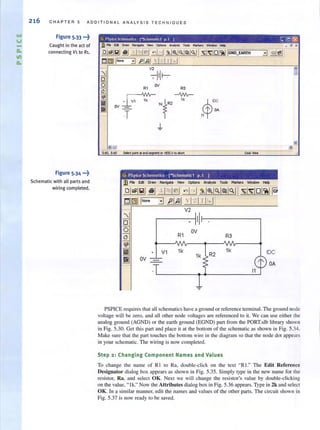
![S EC T I O N 5 . 5 D C S PI CE AN ALYS I S USI N G SCH E MA T IC CAPTUR E 223
-v1 - 2v 2 + 4v3 + 3v4 = -8
» G ; [ 2 -1 0 -1; 0
G ;
2 -1 0 -1
0 1 0 0
0 0 -1 1
-1 -2 4 3
» i = [8; 12; 6; -8 ]
8
12
6
- 8
» v=inv CG)*i
v ;
13.8/.62
12.0000
1.6923
7.6 9 23
» VQut= v (4)
vout =
7 . 6923
1 0 O ·,
Once again, we find that V4 = v.. = 7.692 V.
0 0 -1 1 ., -1 -2 4 3J
As a final example in this section on PSPICE, we will examine a circuit containing
dependent sources that was analyzed in Chapter 3 using both node and loop equations. The
network is shown in Fig. 5.50. We streamline this presentation by ski pping the steps, already
described in detail earlier, that are used to set up resistorsand independent sources, and con-
centrate on the ethod employed to place dependent sources in the schematic.
+
V, 1 kO 1 kO 6 V
1 kO 1 kO 1 kll
12V + 1 kO
EXAMPLE 5.21
~-. Figure 5.50
Circuit for Example 5.21.
•
Using the techmques introduced earlier, the complete PSPICE schematic, shown in Fig. 5.5 1, SOLUTION
can be created. Of particular interest are the dependent sources. The voltage·controlled volt·
age source part (VCVS) is called E in PSPICE. Conceptually, we consider the part to consist
of a virtual voltmeter and a virtual voltage source. This "virtual meter" is connected across
the dependent voltage, V.n and the voltage across the "virtual source" is (he output of the
•
"V
III
"V
n
"'](https://image.slidesharecdn.com/basicengineeringcircuitanalysis9thirwin-160630150938/85/Basic-engineering-circuit-analysis-9th-irwin-245-320.jpg?cb=1719934140)
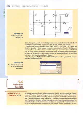
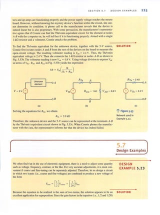
![•
226 CHAPTER 5 ADD IT IONAL ANAL Y SIS TECHN I QUES
Rj
Vcoarsc +
Figure 5·54 'j'
(aJ The coarse/fine adjust-
ment circuit, (b) with Vfine
set to zero and (cJ with
V(oars!! set to zero.
DESIGN
EXAMPLE 5.24
Figure 5.55 .••~
The model circuit for the
attenuator pad design.
R
are both less than one, a voltage divider with two inputs would appear to be a logical choice.
A typical circuit for this application is shown in Fig. 5.54a. The two superposition subcircuits
are shown in Figs. 5.54b and c. Employing voltage division in the network in Fig. 5.54b
yields
and therefore,
In a similar manner, we find that
which requires that
R2
+ Vfine
+
~lIne_F =
Vfine
Vcoarse +
[
R// R, ] J
(R//R,) + R, 2
[
R//R, ]
(R//R,) + R, 20
R, = J9{R// R,)
RJ
+
Vtune Vtunc_C R R2 RJ
(a) (b)
R2
+ Vfine
+
R Vtunc_F
(c)
Note that the two constraint equations for the resistors have three unknowns-R, Rio and
R2. Thus, we must choose one resistor value and then solve for the two remaining values.
If we arbiJrarily selecl R = I kO, then R, = 9000 and R, = 9 kO. This compleJes the
design of the circuit. This example indicates that superposition is not only a useful analysis
tool but provides insight into the design of new circuits.
Coaxial cable is often used in very-high-frequency systems. For example, it is commonly
used for signal transmission with cable television. In these systems resistance matching, the
kind we use for maximum power transfer, is critical. In the laboratory, a common apparatus
used in high-frequency research and development is the attenuator pad. The attenuator pad
is basically a voltage divider, but the equivalent resistance at both its input ports is careful-
ly designed for resistance matching. Given the network in Fig. 5.55 in which a source, mod ~
eled by Vs and Rs (50 0), drives an attenuator pad, which is connected to an equivalent load.
___A!t~'2u_a~o!: ec:d__ _,
5011](https://image.slidesharecdn.com/basicengineeringcircuitanalysis9thirwin-160630150938/85/Basic-engineering-circuit-analysis-9th-irwin-248-320.jpg?cb=1719934140)
![SECT ION 5 . 7 DESIGN EXAMPLES
Let us design the pad so that it has an equivalent resistance of 50 n and divides (i.e., allen-
uates) the input voltage by a factor of 10.
Since the aUenllator or "T-Network" must have an equivalent resistance of 50 n,we require
that RTh.in and R Th-QUt be 50 n. Since these Thevenin resistance values are the same and the
circuit is symmetric, we can use the label R2 twice to indicate that those resistors will be
the same value.
R-fh.;" = R, + [R,//(R, + SO)J= 50
RTh.oo, = R, + [R,//(R, + SO)J = so
Since the equations are identical, we refer to both Thevenin equivalent resistance parame-
ters simply as RTh • The Thevenin equivalent voltage, VTh , can be easily derived trom the cir-
cuit in Fig. 5.56 a using voltage division.
VTh = Vs[
R,
R, ]
+ R, + SO
Rs R2 R2
•
SOLUTION
~... Figure 5.56
(a) The circuit used in
50 0 +
+ finding VTh and (b) the
Vs R, VTh VTh RL You, resulting model.
500
(a) (b)
From the Thev"nin equivalent circuit in Fig. 5.56b, we find
V _ 1' [ 50 ]_ VTh
out - Th R Th + 50 - 2
Combining these equations yields the attenuation from Vs to VOu
Yo", [Vo",][VTh ] I [ R, ] 1
V; = VTh V; = 2 R, + R, + 50 = 10
The Thevenin equivalent resistance equation and this attenuation equation provide us
with two equ lions in the two unknowns RI and R2. Solving these equations yields
R, = 20.83 nand R, = 33.33 n. For precise resistance matching, these resistors must be
very accurate.
With such low resistor values, the power dissipation can become significant as Vs is
increased. For example, if Vs :;:::: to V, Vout ::;; I V and the power dissipated in the R2resis-
tor connected to the input source is 333 mW. To keep the temperature of that resistor at rea-
sonable levels, the power rating of that resistor should be at least 0.5 W.
227
Let us design a circuit that will realize the following equation.
Vo = - 3Vs - 2000ls
DESIGN
EXAMPLE 5.25
•
An examinatio of this equation indicates that we need to add two terms, one of which is SOLUTION
from a voltage source and the other from a current source. Since the terms have negative
signs. it would appear that the use of an inverting op-amp stage would be useful. Thus, one
possible circuit for this application appears to be that shown in Fig. 5.57.
•](https://image.slidesharecdn.com/basicengineeringcircuitanalysis9thirwin-160630150938/85/Basic-engineering-circuit-analysis-9th-irwin-249-320.jpg?cb=1719934140)
![228 C H A PT E R 5 A DD I T IO N A L ANA LYSIS TE CHNIO UE S
Figure 5.57 ...~
Circuit used in
Example 5.25.
Figure 5.58 "'~
Circuits used in deriving a
Norton equivalent circuit.
The Nonon equivalent circuit at the terminals A-B will provide a composite view of the
op-amp's input. Superposition can also be used in conjunction with (he Norton equivalent
to simplify the analysis. Using the network in Fig. 5.58a, we can determine the contribution
of Vs to the short-circuit current, lsc. which we call Isc.'
Vs
I = -
SC I R]
R, A R A R, A
RThVs Isc1 Isc2
-
B B B
(e) (b) (e)
In a similar manner, using Fig. 5.58b, we find that the contribution of Is to the short-circuit
current is
l.f>Cj = Is
Employing superposition, the sum of these two currents yields the actual short-circuit current
Vs
l'of; = - + Is
R,
The Thevenin equivalent resistance al nodes A-B is oblained from the network in Fig. 5.58c as
RTh = R,
The equivalent circuit isnow redrawn in Fig. 5.59 where we have employed the ideal op-
amp conditions (Le., "'in = 0), and the current into the op-amp terminals is zero. Since lin
is directly across RTh , the current in this resistor is also zero. Hence, all the current lsc will
flow through R" producing the voltage
v. = -R2[~~ + Is] = - ; : Vs - IsR,
A comparison of this equation with the design requirement specifies that
R,
- = 3 and R, = 2000 n
R,
which yields R, = 667 n.Combining a I-k!1 and a 2-k!1 resistor in parallel will yield the
necessary 667 !1 exactly.](https://image.slidesharecdn.com/basicengineeringcircuitanalysis9thirwin-160630150938/85/Basic-engineering-circuit-analysis-9th-irwin-250-320.jpg?cb=1719934140)
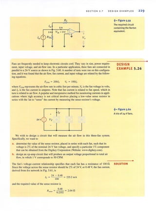
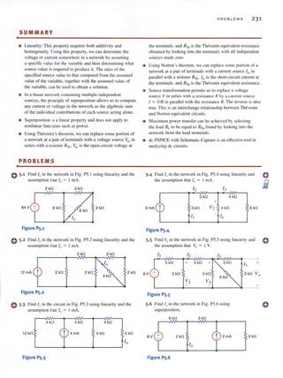
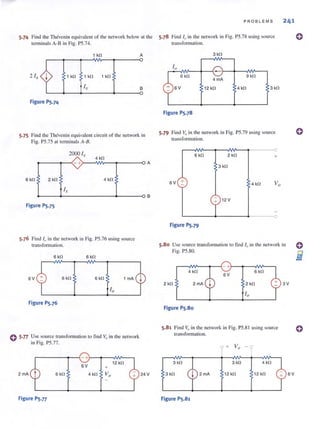
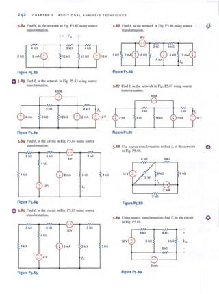
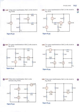
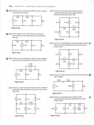
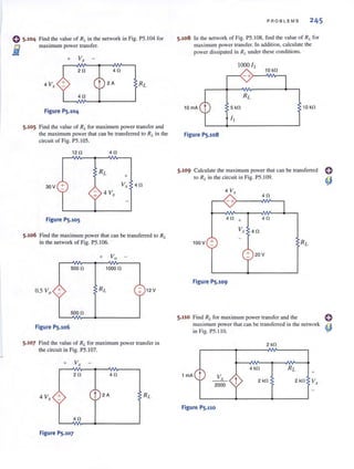

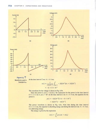
![SECTION 6.2
In the time interval 0 ~ t ~ 2 ms,
W(I ) = l'8X3dX = 21'
Hence,
w(2ms) = 32pJ
In the time interval 2 ~ t ~ 4 ms,
W(I) =l' [(16 X W-6)x - (64 x I0-9
) ] dx + 32 x 10-12
2x lO '
= [(8 x 1O-6
)x' - (64 x 1O-9
)x];XIO-' + 32 x 10-12
= (8 X 10⁻⁶
)1' - (64 X 10-')1 + 128 x 10-12
From this expression we find that w(2 ms) = 32 pJ and w(4 ms) = O. The energy wave-
form is shown in Fig. 6.5d.
Learning ASS ESS MEN IS
E6.2 The voltage across a 2-JJ.F capacitor is shown in Fig. E6.2. ANSWER:
Delemtine the wavefonn for the capacitor current. .B
vir) (V) i(l) (rnA)
121-----.
12
o 2 3 4
IND U C T ORS
6
5
o 2 6 I (ms) -6
I I (ms)L--_ _ _ _----l
Figure E6.2
E6.3 Compute the energy stored in the electric field of the
capacilOr in Learning Assessment E6.2 at I = 2 ms.
ANSWER: 1V = 144 JJ.1.
An ilu/llclOr is a circui t element that consists of a conducting wire usually in the form of a 6 2
coil. Two ty pical inductors and their electrical symbol are shown in Fig. 6.6. Inductors are •
typically categorized by the type of core on which they are wound. For example, the core Inductors
material may be air or any nonmagnetic material, iron, or ferrite. Inductors made with air
or nonmagnetic materials are widely used in radio, television, and filter circuits. Iron-core
inductors are used in electrical power supplies and filters. Ferrite-core inductors are wide-
ly llsed in high-frequency applications. Note that in contrast 10 the magnetic core that con-
fines the flux, as shown in Fig. 6.6b, the flux lines for nonmagnetic inductors extend beyond
the inductor itself, as illustrated in Fig. 6.6a. Like stray capacitance, stray inductance can
result from any element carrying current surrounded by flux linkages. Figure 6.7 shows a
variety of typical inductors.
From a historical standpoint, developments that led to the mathematical model we
employ to represent the inductor are as follows. h was first shown that a current-carrying
conductor would produce a magnetic field. " was later found that the magnetic field and the
current that produced it were linearly related. Finally. it was shown that a chnnging Illagnetic
255](https://image.slidesharecdn.com/basicengineeringcircuitanalysis9thirwin-160630150938/85/Basic-engineering-circuit-analysis-9th-irwin-275-320.jpg?cb=1719934140)
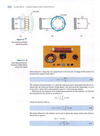
![SECT I ON 6.2 INDUCTORS 257
Therefore, the energy stored in the magnetic field is
l'[ di(X ) ]1OL(I) ~ L - - i(x )dx
-00 dx
Following the development of Eq. (6.6), we obtain
6.12
Now let's consider the case of a dc current fl owing through 3n inductor. From Eq. (6.8),
we see that the voltage across the inductor is directly proportional to the time rate of
change of the current flowing through the inductor. A dc current does not vary with time,
so the voltage across the inductor is zero. We can say that an inductor is "a short circuit to
dc." In analyzing a circuit containing dc sources and inductors, we can replace any induc-
tors with short circuits and calculate voltages and currents in the circuit using our many
analysis tools.
Note from Eq. (6. 11) that an instantaneous change in inductor current would require
infin ite power. Since we don't have any infinite power sources, the current flowing
through an inductor cannot change instantaneously. This will be a particularly helpful idea
in the next chapter when we encounter circuits containing switches. This idea of "conti-
nuity of current" for an inductor tells us that the current flowing through an inductor just
after a switch moves is the same as the current flowing through an inductor just before
that switch moves.
Find the total energy stored in the circuit of Fig. 6.8•.
9V
9V
611
611
+
Vel
(a)
(b)
C2 ~ 50 ~F
+
Va
6 11
611
This circuit has only dc sources. Based on our earlier discussions about capacitors and induc-
tors and constant sources, we can replace the capacitors with open circuits and the inductors
with short circuits. The resulting circuit is shown in Fig. 6.8b.
This resistive circuit can now be solved using any of the techniques we have learned in
earlier chapters. If we apply KCL at node A, we get
I L2 = I Ll + 3
EXAMPLE 6.5
~••• Figure 6.8
Circuits used in
Example 6.5.
SOLUTION
•
•](https://image.slidesharecdn.com/basicengineeringcircuitanalysis9thirwin-160630150938/85/Basic-engineering-circuit-analysis-9th-irwin-277-320.jpg?cb=1719934140)
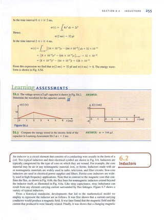
![C H A PTE R 6 CA PACIT A N C E AND I NDUCTA NCE
_r FIUXlines
, -.. ' ..' '
i(t) ,' ," ,..
>-~~~~'~~--- I. .,
+
v(r)
: " ," I " ,I
r' I 11
", :::III ",
'" I , I
111 " ,
" I I "
I I - - I I
..., ,
.-
(a)
.....
, ,
, "- ,
Figure 6.6 l
Two inductors and their
electrical symbol
Figure 6.7 .-~
Some typical inductors.
(Courtesy of Mark Nelms
and )o Ann Loden)
i(r)
(b)
Flux lines
••
i(t)
" 1-0--'+:--,
+
v(t)
(e)
field produced a voltage that was proponional to the time rate of change of the current that
produced the magnetic field; thaI is,
di(/)
v(/) = L -
d/
6.8
The constant of proportionality L iscalled the inductance and is measured in the unit hell /)r,
named after the American inventor Joseph Henry, who discovered the relationship. As seen
in Eq. (6.8), I henry (H) is dimensionally equal 10 I volt-second per ampere.
FoUowing the development of the mathematical equations for the capacitor, we find that
the expression for the current in an inductor is
11'i(/) = - v( x )dx
L ~
6.9
which can also be written as
i(/) = i(/o) + - v(x )dx11'L "
6.10
The power delivered to the inductor can be used to derive the energy stored in tbe element.
This power is equal 10
p(/) = v( /)i(/)
[
di(l ) ]
= Ldt i(/) 6.11](https://image.slidesharecdn.com/basicengineeringcircuitanalysis9thirwin-160630150938/85/Basic-engineering-circuit-analysis-9th-irwin-280-320.jpg?cb=1719934140)
![we find that
and
20 X 10-]
V (I) = (l OX W 3
) -=-=----'-'---c-
2 X 10 ]
= 100 mV
V(I) = (10 X 10-]) - 20 X 10]-]
2 X 10
= - 100mV
SECTION 6 . 2
Q:S;:t$2ms
2$1$4ms
and V(I) = 0 for I > 4 ms. Therefore, the voltage waveform is shown in Fig. 6.9b.
The current in a 2-mH inductor is
i(l) = 2 sin 3771A
Determine the voltage across the inductor and the energy stored in the inductor.
From Eq. (6.8), we have
and from Eg. (6. 12),
"i(I)
V(I ) = L -
dl
d
= (2 X 10⁻³)-(2 sin 3771)
dl
= 1.508 cos3771 V
I ,
WL(t) = 2Li-(I)
I
= - (2 X W ])(2 sin 3771)'
2
= 0.004 sin'3771 J
The voltage across a 200-mH inductor is given by the expression
V(I) = (I - 31)e-]'mV '''' 0
= 0 1 <0
Let us derive the waveforms for the current, energy, and power.
I N 0 U C T O A S 259
EXAMPLE 6.7
•
SOLUTION
EXAMPLE 6.8
•
The wavefonm forthe voltage is shown in Fig. 6.1 Oa. The current is derived from Eg. (6.1 0) as SO LUTI 0 N
10] 1.'i(l) = - (I - 3x)e-]X dx
200 0
= 5{[e-3X
dx - 31.'xe-3
• dx}
= 5{~;l - 3[-e;.(3x + I)D
== 5re-31 rnA r ~ 0
= 0 1 < 0
•
•](https://image.slidesharecdn.com/basicengineeringcircuitanalysis9thirwin-160630150938/85/Basic-engineering-circuit-analysis-9th-irwin-281-320.jpg?cb=1719934140)
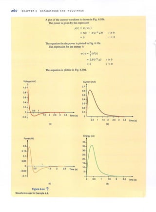
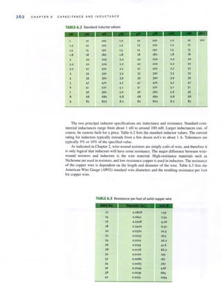
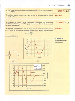
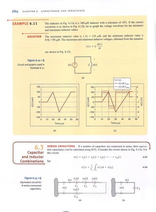
![SECTION 6 .3 CAPACITOR AND INDUCTOR COMB I NA T IONS
Therefore, Eq. (6. 13) can be written as follows using Eq. (6.14):
(
N 1)1' N
V(I) ~ ,?, C, ,. i(l)dl + ,?,V,(lo) 6.15
11'~ c i(/)dl + V(lo)
S '.
6.16
where
N
V(lo) ~ 2:V,(lo)
i"' J
and [h in t 1
I NI l 1 1
- ~ 2: -~-+-+"'+
Cs ':1 C, C1 C, CN
6.17
Thus, the circuit in Fig. 6.13b is equivalent to that in Fig. 6. 13a under the conditions stated
previously.
It is also important to note that since the same current flows in each of the series capaci-
tors, each capacitor gains the same charge in the same time period. The voltage across each
capacitor will depend on this charge and the capacitance of the element.
Detennine the equivalent capacitance and the initial voltage for the circuit shown in Fig. 6. 14.
Capacitors in series com bine
like resistors in parallel.
EXAMPLE 6.12
•
Note that these capacitors must have been charged before they were connected in series or SOLUTION
else the charge of each would be equal and the voltages would be in the same direction.
The equivalent capacitance is
I I I I
-~-+-+
Cs 2 3 6
where all capacitance values are in microfarads.
Therefore, Cs = I ~F and, as seen from the figure, V(lo) ~ -3 V. Note that the total
energy stored in the circuit is
W(IO) = -'- [2 X lQ-<(2)' + 3 X lQ-«-4)' + 6 X lQ-« -I)']
2
= 31 fl.1
However, the energy recoverable at the terminals is
I
Wc(lo) = "2CsV'( I)
I
= "2[1 X lQ-«-3)']
= 4.5 fl.1
~••• Figure 6.14
Circuit containing multiple
capacitors with initial
Voltages.
•](https://image.slidesharecdn.com/basicengineeringcircuitanalysis9thirwin-160630150938/85/Basic-engineering-circuit-analysis-9th-irwin-287-320.jpg?cb=1719934140)
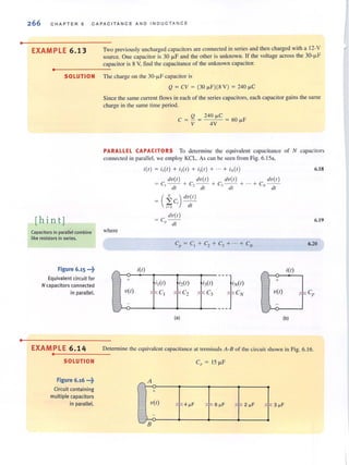
![SECT I ON 6 . 3 C AP ACITO R AND IN DU CTOR COMB I N AT I ONS
Learning As5 ES5 MEN IS
E6.6 Two initially uncharged capacitors are connected as shown in Fig. E6.6. After a period of ANSWER: C, = 4 /-LF.
time, the voltage reaches the value shown. Detennine the value of Cj '
+
24 V
Figure E6.6
E6.7 Compute the equivalent capacitance of the network in Fig. E6.7.
Figure E6.7
SERIES INDUCTORS If N inductors are connected in series. the equivalent inductance
of the combination can be determined as follows. Referring to Fig. 6. 17a and using KYL, we
see (har
and therefore,
where
di(t) di(t ) di(t ) di(t )
v(t ) = L, - - + L, - - + L, -- + ... + LN - -
dl ~ dl . dt dl
(
N ) di(t )
2; Li -
i = l dt
di(t)
= Ls--
dt
N
Ls = L L; = Ll + L2 + .. . + LN
;= 1
6.21
6.22
6.23
6.24
Therefore, under this condition the network in Fig. 6. 17b is equivalent to that in Fig. 6. 17a.
ANSWER: Ceq = J.5 /-LF.
[hint]
Inductors in series combine
like resistors in series.](https://image.slidesharecdn.com/basicengineeringcircuitanalysis9thirwin-160630150938/85/Basic-engineering-circuit-analysis-9th-irwin-289-320.jpg?cb=1719934140)
![•
268 CHAP TER 6 CAPACITANCE AND IN D UCTANCE
Figure 6.17 •••~ i(r) +vI(rL +v2(rL +v3(r) _ r- i(r)
Equivalent circuit + L3
+
for N series-connected
L I L2
S
inductors. v(r) v(r) ! Ls
LN
---------- - -------_.- + ~
vN(r)
(a) (b)
EXAMPLE 6.1 5 Find the equivalent inductance of the circuit shown in Fig. 6. 18.
•
SOLUTION The equivalent inductance of the circuit shown in Fig. 6. 18 is
Figure 6.18 •••~
Circuit containing
multiple inductors.
[hin tj
Inductors in parallel combine
like resistors in parallel.
Figure 6.19 •••~
Equivalent circuits for
N inductors connected
in parallel.
+
V(I)
Ls = IH + 2H + 4H
= 7H
1 H 2 H
4H
PARALLEL INDUCTORS Consider the circuit shown in Fig. 6. 19a, which contains N
parallel inductors. Using KCL, we can write
However,
Substituting this expression into Eq. (6.25) yields
where
(
N I )1' N
i(l) = L: - v(x)dx + L: iito)
j - I Lj In j - I
11'= - v(x)dx + i(10)
L,. to
I I I 1 I
-=-+- +-+ ... + -
L" L, L., L, LN
6.25
6.26
6.27
6.28
6.29
and i(to) is equal to the current in Lp at t = 1
0
, Thus, the circuit in Fig. 6.19b isequivalent to
that in Fig. 6.19<1 under the conditions slated previously.
i(l)
r- i(l)
-Of"~) +
LN V(I) Lp
)
'-'
/ '
+
JI(I) ti2(1) ) i3(1)
V(I) L (
! L2 L 3
1 ']-
'-'
(a) (b)](https://image.slidesharecdn.com/basicengineeringcircuitanalysis9thirwin-160630150938/85/Basic-engineering-circuit-analysis-9th-irwin-290-320.jpg?cb=1719934140)
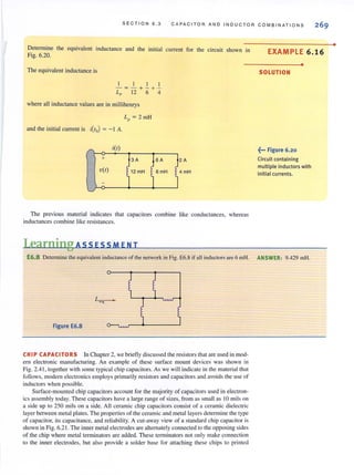
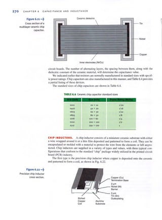
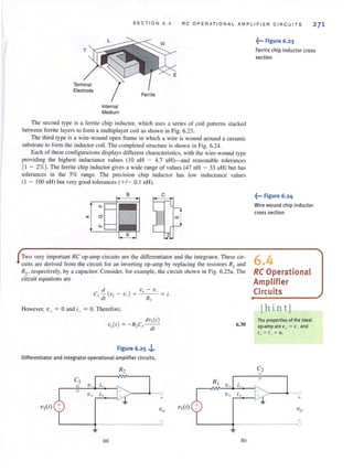
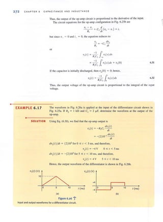
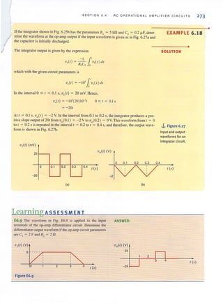
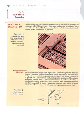
![SECTION 6 . 5 APPLI C ATION EXAMPLES 275
In order to quantify the level of crosstalk, we want to know how much of the voltage on
wire I appears on wire 2. A nodal analysis at wire 2 yields
. ( ) _ c [dVI (I) dV,(I)]. [dV,(I)]
112 I - 12 - - - - - = 1.,(1) = C, - -
d l dl - - cll
Solving for dV,(I)/ dl, we find that
dv,(I) = [ C" ] dv,(I)
dl c" + C, dl
Integrating both sides of this equation yields
V,(I) = [C"C~' C,]VI(I)
Note that it is a simple capacitance ratio that determines how effectively V,(I) is "coupled"
into wire 2. Clearly, ensuring that C" is much less than C, is the key to controlling
crosstalk. How is this done? First, we can make Cl2 as small as possible by increasing the
spacing between wires. Second, we can increase C2 by putting it closer to the ground
wiring. Unfortunately, the first option takes up more real estate. and the second one slows
down the voltage signals in wire I. At this point, we seem to have a typical engineering
tradeoff: to improve one criterion, that is, decreased crosstalk, we must sacrifice another,
space or speed. One way to address the space issue would be to insert a ground connection
between the signal-carrying wires as shown in Fig. 6.30. However, any advantage achieved
with grounded wires must be traded off against the increase in space, since inserting
grounded wires between adjacent conductors would nearly double the width consumed
without them.
Redrawing the circuit in Fig. 6.3 1 immediately indicates that wires I and 2 are now elec-
trically isolated and there should be no crosstalk whatsoever-a situation that is highly
unlikely. Thus, we are prompted to ask the question, "Is our model accurate enough to
model crosstalk?" A more accurate model for the crosstalk reduction scheme is shown in
Fig. 6.32 where the capacitance between signal wires I and 2 is no longer ignored. Once
again, we will determine the amount of crosstalk by examining the ratio V2(1)/VI(t).
Employing nodal analysis at wire 2 in the circuit in Fig. 6.33 yields
. _ [dVI (I ) dV,(I)] _. _ ( l[dV,(I)]
1,,(1) - C" - - - - d- - ,,(1) - C, + C'G I
- - dl I - - - (, I
CtI CtGT C;~T C2 I~V2(1)
~und
= = wire =
~••• Figure 6.30
Use of a ground wire in the
crosstalk model.
~... Figure 6.31
Electrical isolation using
a ground wire in crosstalk
model.](https://image.slidesharecdn.com/basicengineeringcircuitanalysis9thirwin-160630150938/85/Basic-engineering-circuit-analysis-9th-irwin-297-320.jpg?cb=1719934140)
![•
276 CHAPTER 6 CAPAC ITANCE AND INDUCTANCE
Figure 6.32 •••~
A more accurate
crosstalk model.
APPLICATION
EXAMPLE 6.20
•
Solving for dv,(r)!dr, we obtain
dv,(r) = [ C12 ] dv,(r)
dl C12 + C2 + C2G dt
Integrating both sides of this equation yields
[
C,' ]
v,(r) = C
12
+ C,- + C
2G
v,(r)
Note that this result is very similar to our earlier result with the addition of the C2G term.
Two benefits in this situation reduce crosstalk. First, en is smaller because adding the
ground wire moves wires 1 and 2 farther apart. Second, C2G makes the denominator of
the crosstalk equation bigger. If we assume that C'G = C, and that C12 has been halved by the
extra spacing, we can expect the crosstalk to be reduced by a factor of roughly 4.
An excellent example of capacitor operation is the memory inside a personal computer. This
memory, called dynamic random access memory (DRAM), contains as many as four billion
data storage sites called cells (circa 2007). Expect this number to roughly double every two
years for the next decade or two. Let us examine in some detail the operation of a sing le
DRAM cell.
SOLUTION Figure 6.34a shows a simple model for a DRAM cell. Data are stored on the cell capacitor
in true/false (or 1/0) fannat, where a large-capacitor voltage represents a true condition and](https://image.slidesharecdn.com/basicengineeringcircuitanalysis9thirwin-160630150938/85/Basic-engineering-circuit-analysis-9th-irwin-298-320.jpg?cb=1719934140)
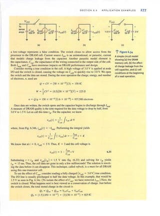
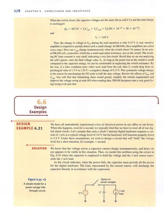
![SECTION 6.6 DESIGN EXAMPLES
V(I) = 3.0 - ~ J i(l) (/1
After I second, V(I) should be at least 2.4 V, that is, the minimum functioning voltage, and
hence
11'2.4 = 3.0 - - (0.001 ) (/1
C "
Solving this equation for C yields
c = 1670}J.F
Thus, from the standard capacitor values in Table 6.1 , connecting three 560-~F capaciLOrs
in parallel produces 1680 }J.F. Although three 560-}J.F capacitors in parallel will satisfy the
design requirements. this solution may require more space than is available. An alternate
solution involves the use of "double-layer capacitors" or wha! are known as Supercaps.
A Web search of this topic will indic,lte that a company by the name of Elna America, Inc.
is a major supplier of double-layer capaciLOrs. An investigation of their product listing
indicates that their DCK series of small coin-shaped supercaps is a possible alternative in
this situation. In particular, the DCK3R3224 supercap is a 220-mF capacitor rated at 3.3 V
with a diameter of 7 mm, or about 1/4 inch, and a thickness of 2.1 mOl. Since only one of
these items is required, this is a very compact solution from a space standpoint. However,
there is yet another factor of imparlance and that is cost To minimize cost, we may need to
look for yet another alternate solution.
Let us design an op-amp circuit in which the relationship between the output voltage and 0E5IGN
two inputs is EXAMPLE 6.22
V"(I ) = 5J V,(I) (/1 - 2v,(I )
•
In order to satisfy the output voltage equation, we must add two inputs, one of which must SOLUTION
be integrated. Thus, the design equation calls for an integrator and a summer as shown in
Fig. 6.36.
Using the known equations for both the integrator and summer, we can express the out-
put voltage as
'V"(I ) = -V'(I)[~:l- [~:]{- R:C JV,(I)(/I} = R,::C J V,(I)(/I - [~:lV'(I)
C R4
RI
R2
+
+
VI(I) + R3
~
Vo(l)
V2(1)
~ ~ ~
~... Figure 6.36
Op-amp circuit with
integrator and summer.
279
•](https://image.slidesharecdn.com/basicengineeringcircuitanalysis9thirwin-160630150938/85/Basic-engineering-circuit-analysis-9th-irwin-301-320.jpg?cb=1719934140)
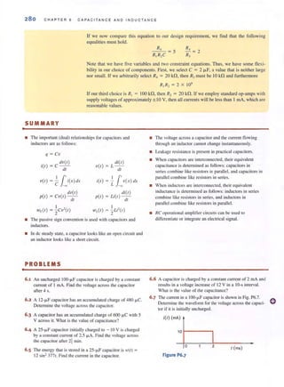
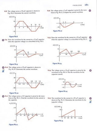
![o 6.69 A 20·1111-1 inductor and a 12-mH inductor are connecled
in series with a I-A current source. Find (a) the equiva-
lent inductance and (b) (he total energy stored.
o 6·70 For the network in Fig. P6.70, Vs(l ) = 120 cos 3771 V.
Find VO(I).
1 kil
1 ~F
+
vs(t)
Figure P6.70
6.71 For the network in Fig. P6.71 choose C such that
Vo = - 10JVs dl.
Source model c
RS ~ 10kO 70kO
>---+___0
+
L-------~------~--------__4.___o_________ _ ___ J
Figure P6.71
o 6.72 For 1he network in Fig. P6.72 Vs,(I) = 80 cos 377t V
and Vs,(I) = 40 cos 377t V. Find Vo( I).
20 kil 10 kO
>--~---o
+
vs,(t) vs,(t)
Figure P6.72
o 6·73 The circuit shown in Fig. P6.73 is known as a "Deboo"
integrator.
(a) Express the output voltage in terms of the input volt-
age and circuit parameters.
(b) I-Iow is (he Deboo integrator's performance different
from that of a standard integrator?
(e) What kind of application would justify the use of
this device?
PROBLEMS
> - -;--{) +
+ o--~~-~-~-t~
R
Vs
Figure P6.73
6 .74 An integrator is required that has the following
perfonnance
VO( I) = 10'J v, dt
~-
where the capacitor values mus( be greater than
10 nF and the resistor values must be greater than
10kfl.
(a) Design the integrator.
(b) If ± 10·Y supplies are used, what are the maximum
and minimum values of vo?
(e) Suppose Vs = I V. What is the rate of change of vo?
6.75 A driverless automobile is under development. One criti-
cal issue is braking, particularly at red lights. It is decid-
ed that the braking effort should depend on distance to
the light (if you're close, you better stop now) and speed
(if you're going fast, you' ll need more brakes). The
resulting design equation is
[
dX(I)]
braking effort = K I ~ + K,x(t)
where x, the distance from the vehicle to the intersection.
is measured by a sensor whose output is proportional to
X, vsense = ax. Use superposi(ion to show that the circuit
in Fig. P6.75 can produce the braking effort signal.
R"
Figure P6.75
o](https://image.slidesharecdn.com/basicengineeringcircuitanalysis9thirwin-160630150938/85/Basic-engineering-circuit-analysis-9th-irwin-311-320.jpg?cb=1719934140)

![S E C T I O N 7.2 FIRS T· ORDER CI R CUITS 293
RS
(al
+ R
vc(r)
[(R) Xenon lamp]
Discharge
time
"_,___ __ charge__ __--I
I1- time •
I
I
I
I
I
I
I
(bl
cr:: R
(c)
we might call a free-body diagram of the right half of the network in Fig. 7.la as shown
in Fig. 7. 1c (that is, a charged capacitor that is discharged through a resistor). When the
switch is closed, KCL for the circuit is
dvc(r) vc(r)
C--+ -- ~ O
dr R
or
dvd r) I
- - + - v (r) ~ 0
dr RC C
In the next section we will demonstrate that the solution of this equation is
Vdl ) = v" e-f
/
RC
Note that this function is a decaying exponential and the rate at which it decays is a function
of the values of R and C. The product RC is a very important parameter, and we will give it
a special name in the following discussions.
GENERAL FORM OF THE RESPONSE EQUATIONS In our study of first-order tran- 7 2
sient circuits we will show that the solution of these circuits (i.e., finding a voltage or cur- •
~... Figure 7.1
Diagrams used to
describe a ca mera's
flash circuit.
rent) requires us to solve a first-order differential equation of the form First-Order
dx(r) Circuits
- - + ax(r) ~ fer )
dr 7.1
Although a number of techniques may be used for solving an equation of this type, we will
obtain a general solution that we will then employ in two different approaches to transient
analysis.
A fundamental theorem of differential equations states that if x(r) ~ xp(r) is any solution
to Eq. (7. 1), and x(r) ~ x,(r) is any solution to the homogeneous equation
dx(r)
- - + ax(r) ~ 0
dr
7.2](https://image.slidesharecdn.com/basicengineeringcircuitanalysis9thirwin-160630150938/85/Basic-engineering-circuit-analysis-9th-irwin-315-320.jpg?cb=1719934140)
![294 CHAPTER 7 FIRST- AND SECOND-ORDER TRANSIENT CIRC U ITS
then
X(I) = X,(I ) + X,(I ) 7.3
is a solution to Ihe original Eq. (7.1 ). The term xp(t) is called the particl/lor integral soll/-
tion, or forced response, and ,A I) is called the comple11lellfwy so/wion t or natural response.
At the present time we confine ourselves to the situation in which f(1) = A (i.c.• some
constant). The general solution of the differential equation then consists of Iwo parts that are
obtained by solving the two equations
dxP(l )
- - + ax,,(I) = A
til
tlx,(I )
- - + aX,(I ) = a
tit
7.4
7.5
Since the right-hand side of Eq. (7.4) is a constant, il is reasonable to assume that the solu-
tion xp{t) must also be a constant. Therefore, we assume that
7.6
Substituting this constant into Eq. (7.4) yields
7.7
Examining Eq. (7.5), we note Ihat
tlx,(I) /til
x,(I)
= - a 7.S
This equation is equivalent to
::1 [lnx, (ll ] = - a
Hence,
In x,.(I) = - at + c
and therefore,
7.9
Thus, a Solulion of Eq. (7. 1) is
7.10
The constant K'2 can be found iF the value of the independent variable X{/) is known at one
instant of lime.
Equation (7.10) can be expressed in general in the foml
x(t) = K, + K,e-'" 7.11
Once the solution in Eq. (7. 11 ) is obtained, certain elements of the eq uation are given
names that are commonly employed in electrical engineering. For example. the term K I is
referred to as the steady-state solutioll: the value of the variable x(t) as 1---7 00 when the
second terlll becomes negligible. The constant T is called the time constant of the circuit.
Note that the second term in Eq. (7.11 ) is a decaying exponential that has a value, if T > 0,
of K 2 for I = 0 and a value of0 for I = 00. The rate at which this exponential decays is deter-
mined by the time constant "i. A graphical picture of this effect is shown in Fig. 7.2a. As can
be seen from the figure. the value of x,(t ) has fallen from K, to a value of 0.368K, in one
time constant, a drop of63.2%. In (WO (ime constants the value of xAt ) has fallen 10 O. 135K2 ,](https://image.slidesharecdn.com/basicengineeringcircuitanalysis9thirwin-160630150938/85/Basic-engineering-circuit-analysis-9th-irwin-316-320.jpg?cb=1719934140)
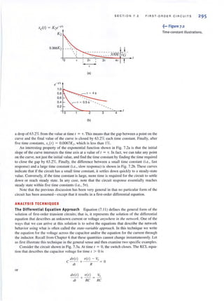
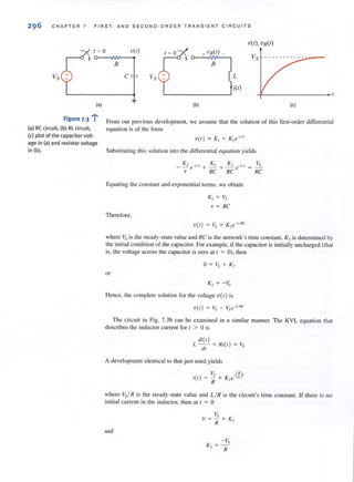
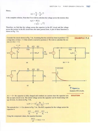
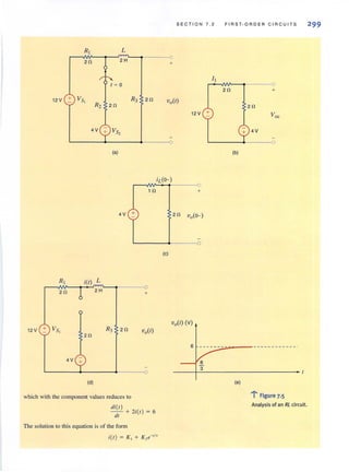
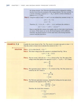
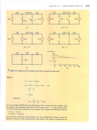
![•
CHAPTER 7 FIRST- AND SECOND-ORDER TRANSI ENT CIACUITS
Figure 7-7 ...~
MATLAB plot for Example 7.3.
EXAMPLE 7.4
following syntax: l ; n spa c e ( x 1 , x 2, N) where x1 and x 2 denote the beginning and
ending points in the interval and N represents the number of points. Thus, to generate an
array containing 150 points in the interval [0, tend], we execute the following command:
»t = linspaceCO, tend, 150)
The MATLAB program for generating a plot of the function is
»tau = 0.15;
»te nd = 10*ta u;
»t = lin spaceC O, tend, 150);
»i = 9/2 + (5/6)*expC-t/tau>;
»plotCt,i)
»xlabelC'Time Cs) 1)
»y l abe lC'Current CrnA) ' )
The MATLAB plot is shown in Fig. 7.7 and can be compared to the sketch in Fig. 7.6(1).
Examination of Fig. 7.6(f) indicates once again that although the voltage across the capac-
itor is continuous at I = 0, the current i(l) in the 6-kft resistor jumps at I = 0 from 2 mA
to 5 1/ 3 mA, and finally decays to 4 1/ 2 rnA.
He fdt ...... ~ fCidl ~ 'Nh:;Igw . .
0"'''8 ~ etE>.('):!) ' - D ~ o l!:ll
5.5r------~------~-----___,
5.4
5.3
5.2
4.8
4.7
4.6
0.5 1.5
Tim. (sJ
The circuit shown in Fig. 7.8a is assumed to have been in a steady-state condition prior to
switch closure at I = O. We wish to calculate the voltage V(I) for I> O.](https://image.slidesharecdn.com/basicengineeringcircuitanalysis9thirwin-160630150938/85/Basic-engineering-circuit-analysis-9th-irwin-326-320.jpg?cb=1719934140)
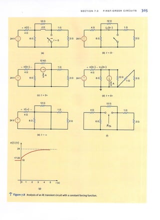
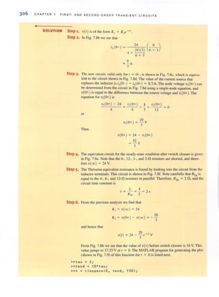
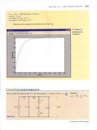
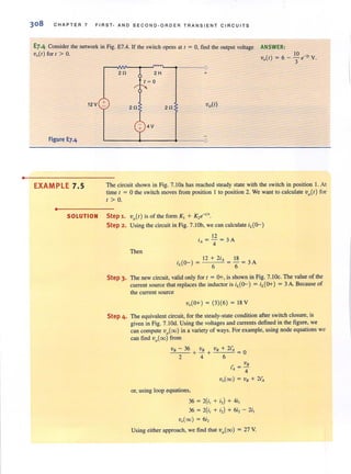
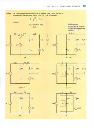
![310 CHAPTER 7 FIRST- AND S ECON D-ORDER TRANSIENT CIRCUITS
From Fig. 7.1 Of we can write the following loop equations:
36 = 2(iA' + i~) + 4iA'
36 == 2(i~ + ise) + 6ir.c - 2i~
Solving these equations for is< yields
Therefore,
. 9
l sc == ZA
Voc 36
RTh = - = - = 8n
i~ 9/ 2
Hence, the circuit time constant is
L 3
T = - == - 5
RTh 8
Step 6. Using the information just computed, we can derive the final equation for Vo( I):
K, = v,,(oo) = 27
K, = v,,(O+) - v,,(oo) = 18 - 27 =-9
Therefore,
V,,(I) = 27 - ge-·/(3/8) V
Learning ASS ESS MEN T
E7.5 If the switch in the network in Fig. E7.5 closes at I = 0, find V.(I) for I > 0. i ANSWER:
V,,(I) = 24 + 36e- ('/ I2 ) V.
4n
24V
r-------~--~V---~_;-+r-----~-+>_~--O
1=0
+
4 n VA
+
L----+----~-------~.__o
Figure E7.5
At this point. it is appropriate to state Ihat not all switch action will always occur at lime
I = O. It muy occur at any time 10 , In this case the results of the step-by-step analysis yield
the following equations:
and
x(to) = K, + K,
x(oo) = K,
.r(I) = x(oo ) + [X(lo) - x(oo) ]e-{·-·,I/,
The function is essentially time-shifted by to seconds.
, > to
Finally, note that if morc than one independcIll source is present in the network, we can
simply employ superposition to obtain the lotal response.](https://image.slidesharecdn.com/basicengineeringcircuitanalysis9thirwin-160630150938/85/Basic-engineering-circuit-analysis-9th-irwin-332-320.jpg?cb=1719934140)
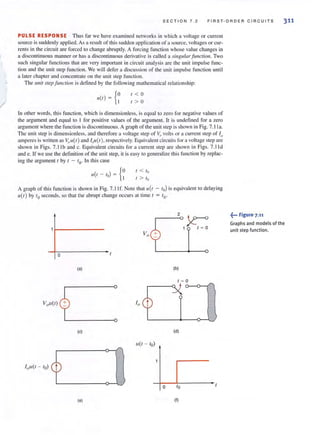
![•
312 CHAP TER 7 F IR ST· A ND SECOND·ORDER TRAN SIENT CI R C UIT S
v(t)
A 1-----,
T
(a)
v(t)
Au(t)
A /--+-----'----'
-A
(b)
T
-AlI(t - 7)
Figure 7.12 1-
Construction of a pulse via
two step functions.
EXAMPLE 7.6
v(t)
vetO) = 0
Step functions can be used to construct one or more pulses. For example. the voltage pulse
shown in Fig. 7.12a can be formulated by initiating a unit step at t = 0 and subtracting one
that starts at t = T. as shown in Fig. 7.12b. The equation for the pulse is
v(t) = A[II(t) - u(t - T)j
If the pulse is to start at t = to and have width T. the equation would be
v(t) = A{u(t - to) - u[t - (to + T)]}
Using this approach, we can write the equation for a pulse starting at any time and ending at
any time. Similarl y. using this approach. we could write the equation for a series of pulses.
called a pulse trai". by simply forming a summation of pulses constructed in the manner
illustrated previously.
The following example will serve to illustrate many of the concepts we have just
presented.
Consider the circuit shown in Fig. 7.13a. The input function is the voltage pulse shown in
Fig. 7. 13b. Since the source is zero for all negative time, the initial conditions for the
6 kO 4 kO
+ +
v(t) (v)
9
vc(t) 8kO vo(t)
100 ~F
0 0.3 t(s)
(a) (b)
4kO 6kO 4kO
+ +
"~ 8kO vo(O+) = 0 9V 8kO voH
(c) t = 0 (d)
6 kO 4 kO
vo{t) (V)
4 ------- - --------------
-------
RTh -
8kO 2.11
t(s)
(e) (I)
..:-. .
! Figure 7.13 Pulse response of a network.](https://image.slidesharecdn.com/basicengineeringcircuitanalysis9thirwin-160630150938/85/Basic-engineering-circuit-analysis-9th-irwin-334-320.jpg?cb=1719934140)
![SECTION 7.2 FIRST · ORDER CIRCUITS
network are zero [i.e., vdD--) ~ 0]. The response vo{t) for 0 < t < 0.3s is due to the
application of the constant source at t = 0 and is not influenced by any source changes that
will occur later. At t ~ 0.3 s the forcing function becomes zero, and therefore vo{t) for
t > 0.3 s is the source-free or natural response of the network.
Let us determine the expression for the voltage vo{t) .
Since the output voltage vo{t) is a voltage division of the capacitor voltage, and the initial volt- SOLUTION
age across the capacitor is zero, we know that vo{o+) ~ 0, as shown in Fig. 7.13c.
If no changes were made in the source after t ~ 0, the steady-state value of vo{t) [i.e.,
vo{00)1due to the application of the unit step at t ~ 0 would be
9
vo(oo ) ~ 6k + 4k + 8k (Sk)
~ 4V
as shown in Fig. 7.13d.
The Th6venin equivalent resistance is
(6k)(12k)
RTh ~ 6k + 12k
~ 4kO
as illustrated in Fig. 7.i3e.
Therefore, the circuit time constant T is
T ~ RThC
~ (4)( 103
)( 100)(10-6
)
~ 0.4 s
Therefore, the response vo(I) for the period 0 < t < 0.3 s is
V,(I) ~ 4 - 4e-'/0.4 V 0 < I < 0.3 s
The capacitor voltage can be caiculated by reaiizing that using voltage division,
vo{t) ~ 2/3 vdl). Therefore,
3
vetl) ~ -(4 - 4e-'/O') V
2
Since the capacitor voltage is continuous,
and therefore,
vet0.3-) ~ vet0.3+ )
2
v,( 0.3+) ~ "3vet0.3- )
~ 4(1 - e-0.3/O.,)
~ 2.1 1 V
Since the source is zero for t > 0.3 S, the final value for vo(t) as t -4- 00 is zero. Therefore,
the expression forvo{l) fort > O.3sis
V,(1) ~ 2.lle-(,-0.3)/0.4 V I> 0.3 s
The term e- (I- O.3)/0.4 indicates that the exponential decay starts at t = 0.3 s. The complete
solution can be written by means of superposition as
V,(1) ~ 4(1 - e-'/O'),,(t) - 4(1 - e-(.-o·3)/0.4)" (1 - 0.3) V
•
313](https://image.slidesharecdn.com/basicengineeringcircuitanalysis9thirwin-160630150938/85/Basic-engineering-circuit-analysis-9th-irwin-335-320.jpg?cb=1719934140)
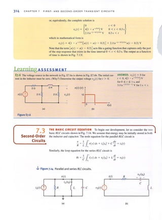
![/
SEC TION 7 . 3 SECOND-ORDER CIRCUITS
Note that the equation for the node voltage in the parallel circuit is of the same form as that
for the loop current in the series circuit. Therefore, the solution of these two circuits is
dependent on solving one equation. If the two preceding equations are differentiated with
respect to time, we obtain
d2
v I dv v dis
c- + -- + - = -
dr 2 R dt L dr
and
d2
j di i dvs
L-+ R-+-=-
dt 2
cit C cit
Since both circuits lead to a second-order differential equation with constant coefficients, we
will concentrate our analysis on this type of equation.
TH E RES PON SE EQUATIO NS In concert with our development of the solution of a first-
order differential equation that results from the analysis of either an RL or an RC circuit as
outlined earlier, we will now employ the same approach here to obtain the solution of a second-
order differential equation that results from the analysis of RLC circuits. As a general rule, for
this case we are confronted with an equation of the form
d'x(l ) dX(I)
- -,- + (I, - - + ",X(I) = f (l )
dr tlr
7.12
Once again we use the fact that if X(I) = Xp(l ) is a solution to Eq. (7. 12), and if
X(I) = Xe(l) is a solution to the homogeneous equation
d'x(l) dX(I)
--,- + ", -- + (l2x(r) =: 0
dr- tit
then
X(I) = Xp(l) + X,.(I )
is a solution to the original Eq. (7. 12). If we again confine ourselves to a constant forcing
function [i.e., f( l ) = A], the development at the beginning of this chapter shows thai the
solution of Eq. (7.12) will be of the form
A
X( I) = - + X,(I)
",
Let us now turn our attention to the solution of the homogeneous equation
d' x(l ) dX(I)
- -,- + ", -- + " , X(I ) = 0
dl- dl
where 01 and (12 are constants. For simplicity we will rewrite the equation in the form
d' x(l ) dX(I) ,
- - + o~w - - + w- r(l ) = 0dr2 - 0 dt o·
7.13
7.14
where we have made the following simple substitutions for the constants (I I = 2~wo and,
12 = Wo o
Following the development of a solution for the first-order homogeneous differential
equation earlier in this chapter, the solution of Eq. (7. 14) must be a function whose first- and
second-order derivatives have the same form, so that the left-hand side of Eq. (7. 14) will
become identically zero for all r. Again we assume that
X(I) = Ke"
Substituting this expression into Eq. (7. 14) yields
315](https://image.slidesharecdn.com/basicengineeringcircuitanalysis9thirwin-160630150938/85/Basic-engineering-circuit-analysis-9th-irwin-337-320.jpg?cb=1719934140)
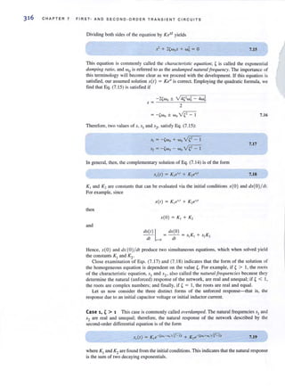
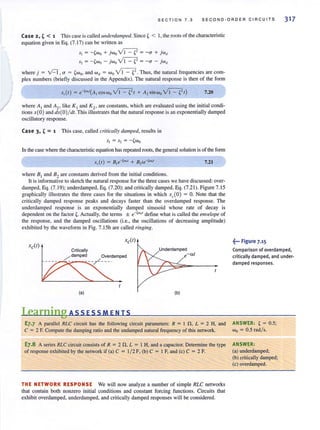
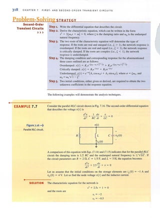
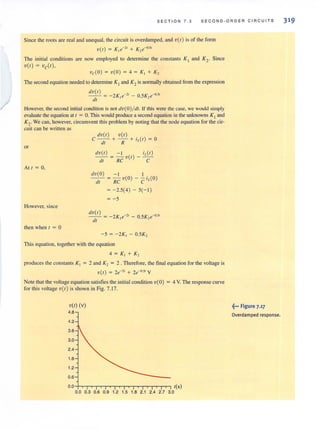
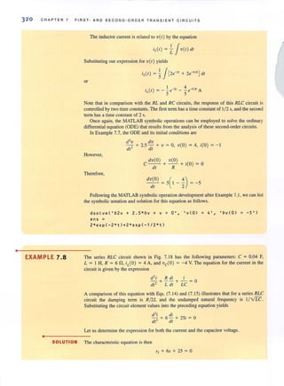
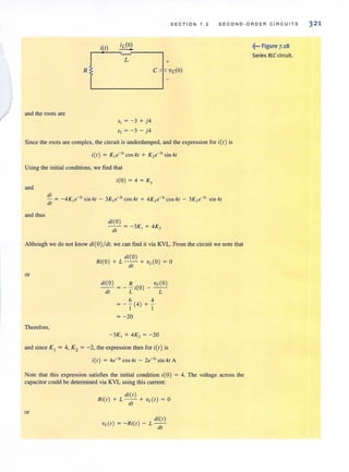
![324 CHAPTER 7 FIRST- AN D SE C OND-O R DE R TRAN S IENT CIRCU I T S
Figure ].21-7
Critically damped
response.
Setting these two expressions equal to one another and evaluating the resultant equation at
1 = 0 yields
1/ 2 I
178 - 1= - 3K, + K,
3 = -3K , + K,
Since KI = I, K2 = 6 and the expression for v(I) is
V( I ) = e-3, + 6Ie-3, V
Note that the expression satisfies the initial condition v(O) = '-
The current jet) can be determined from the nodal analysis equation at Vet) .
dv( t ) v(t)
itt) = c-- +-
dl R,
Substituting V(I) from the preceding equation, we find
I I
i(t ) = - (-3e-31 + 6e-31 - 18te-3t ] + - [e-3t + 6te-3, ]
8 8
or
I 3
itt) = -e-]' - - Ie- ll A
2 2
If this expression for the current is employed in the circuit equation,
di(t)
v(t) = - L dr - R,i(t)
we obtain
v(t) = e-3, + 6te-3, V
which is identical to the expression derived earlier.
The MATLAB program for generating a plot of this function, shown in Fig_7.21, is listed
here.
»tau = 1 / 3;
»tend :: 10*t a u;
»t :: linspace(O, tend, 150);
»v = e x p(-3*t) + 6*t.*exp(-3*t);
»plotCt,v)
» x label ( 'Time (s)')
»ylabel( 'Voltage (V)')
V(I) (V)
1.4
1.2
1.0
0.8
0.6
0.4
0.2
0.0
-0.2 +T""T""T"",-,-,-,-,-r""r-r--.-r-r-,-,..,....,....,
0.0 0.3 0.6 0.9 1.2 1.5 1.8 2.1 2.4 2.7 3.0
I(S)](https://image.slidesharecdn.com/basicengineeringcircuitanalysis9thirwin-160630150938/85/Basic-engineering-circuit-analysis-9th-irwin-346-320.jpg?cb=1719934140)
![SECTION 7.3 SECOND-ORDER CIRCUITS
II' the circuit parameters are R, = 10 n,R, = 2 n,L = 2 H, and C = 1/ 4 F, the differential
equation for the output voltage reduces to
d'v(l ) dV(I)
- - + 7 - - + 12v(l) = 48
dt2
dt
Let us determine the output voltage v(t).
The characteristic equation is
S2 + 7s + 12 = a
and hence the roots are
The circuit response is overdamped, and therefore the general solution is of the form
v (t) = K] e-31 + K2e-~' + K3
The steady-state value of the voltage, K" can be computed from Fig. 7.24a. Note that
v(oo ) = 4V = K,
i(-) ~ 2A 10il i(O~) ~ 1 A 10il
+
SOLUTION
+
24 V 2il v(- ) ~ 4V 12V
+
VcCO~) ~ 2V 2il V(O~) ~ 2V
L----+-_~~--o L----+--~----o
(a)t ~- (b) t ~ 0-
i(O+) ~ lA
10il i(O+)
+
24 V 2V 2il V(0+) ~ 2V
~--------~--~---~o
(c) t ~ 0+
"l": Figure 7.24 Equivalent circuits at t = 00, t = 0-, and t = 0+ for the circuit in Fig. 7-23.
The initial conditions can be calculated from Figs. 7.24b and c, which are valid at
I = 0- and I = 0+, respectively. Note that v(O+ ) = 2 V and, hence, from the response
equation
V(O+) = 2 V = K, + K, + 4
~2= K l+ K2
Figure 7.24c illustrates that i(O+) = I. From the response equation we see that
dv(O )
- - = -3K - 4K,
dt 1 _
•
32 7](https://image.slidesharecdn.com/basicengineeringcircuitanalysis9thirwin-160630150938/85/Basic-engineering-circuit-analysis-9th-irwin-349-320.jpg?cb=1719934140)

![1&.1
V
a.
11
a.
332 CHAPT ER 7 FIRST· AND S E COND · O RDER TRANSIENT CIRCUITS
Figure 7.32 •••~
The PROBE window. Ih... .. ... - ._eo .....-... .. -- _ I~
~ . Iiii~ g . t~... !...; p......-.r-. ~ II
I' ~ Cia q wt's w~ ):::;~ '8I .•:od"'Til~·~:f-~'P- ~'l. A~ ll'..t!
'9
P
..<iI
••Ill ' Mainp
Display
Window
.. ,... .... ....,,-
• " ...... Ci_
• ~~
, . ,
,
Output
Simulation Status Window
Window
I : iTilI.........~
o.
000'10 n n..n.. _ -H$._~ I tn;;.l.m--m
PLOTTING IN PROBE When the PSPICE simulation is finished, the PROBE window
shown in Fig. 7.32 will open. If not, select Run Probe from the Analysis menu. In Fig. 7.32,
we see three subwindows: the main display window, the output window, and the simulation
status window. The waveforms we choose to plot appear in the main display window. The out-
put window shows messages from PSPICE about the success or failure of the simulation.
Run-time information about the simulation appears in the simulation status window. Here we
will focus on the main display window.
To plot the voltage, ve(t) , select Add Trace from the Trace menu. The ADD TRACES
window is shown in Fig. 7.33. Note that the options Alias Names and Subcircuit Nodes
have been deselecled, which greatly simplifies the ADD TRACES wi ndow. The capacitor
voltage is obtained by clicking on V(Vc) in the left column. The PROBE wi ndow should look
like that shown in Fig. 7.34.
Before adding the current itt) to the plot, we note that the dc source is IOV and the resist·
ance is 1 kfl, which results in a loop current of a few milliamps. Since the capacitor voltage
span is much greater, we will plot the current on a second y axis. From the Plot menu, select
Add Y Axis. To add the current to the plot, select Add Trace from the Trace menu, then
select I(CI). Figure 7.35 shows the PROBE plot for vert) and itt ).
FINDING THE TIME CONSTANT Given that Ihe final valueof ve(t ) is IOV, we can write
vc(t) = 10[1 - e-"' ] V
When I = 'T,
To determine the time at which the capacitor voltage is 6.32 Y, we activate the cursors by
selecting CursorlDisplay in the Trace menu. Two cursors can be used to extract x-y data
from (he plots. Use the ~ and ~ arrow keys to move the first cursor. By holding the SHTFf
key down, the arrow keys move the second cursor. Moving the first cursor along the voltage
plot, as shown in Fig. 7.36, we find that 6.32 V occurs at a time of I ms. Therefore, the time
constant is I ms--exactly the RC product.](https://image.slidesharecdn.com/basicengineeringcircuitanalysis9thirwin-160630150938/85/Basic-engineering-circuit-analysis-9th-irwin-354-320.jpg?cb=1719934140)
![....
V
A-
11
A-
334 C HAPTER 7 FI RS T- AN D SECO ND -O RD E R TR ANS I EN T CIR CU IT S
• .,. UI ~ ~ 11_ 8It f" ___ ,... II
JJ " ~ ~ 1.14. '" :.. .! jr.';_;;;;;a......--- ' n
~
~~a ~ Ilt !& M~ I::::: ~"' '''''. -ef ~~:J{.~:rtf:i't~+~~~
::~-----------~-----=======::==:;==========~==~~--~Is 2._ "._ '.IIM
.. m " " (k ) (l] • 1( C1)
u_
- - ,-,--
Figure 7.35 l'
The capacitor voltage and the clockwise loop current.
::: "d''''''~l (,uu,t O,UO I>SI'~ " AII)lI,~".. 1114"",.,,, ( '" ull (.. It"" 1
jaBo to': ~ ~ 11_ !!<II '.. ~ "'" III
--JJ . ~ ~ L.1 . .. ~ .! v- '"""" , n
'~Oiq, 1!I !'ft "~ J:::: ~ IIP ·.... .;f ;t;:~T~R' J1: " ~~ '!
• 1. ... .,-
.. C
OJ
•
•iii 7.S'
,.W
1 . ....
... '.-1 Ir·,,'f· ,.-
2.S1
I~~»
• •
.t.........Ci...
.- "
F· 6"'~.gure 7.3 :
K ....CD @ II(Ilc) [D I ltl )
PROBE plot for v,ctJ and time·constant extraction.
....U_
_.J;lIQ:oCIJ
lflO'1, . . . . . . . .. .
r:-~ ~
- I~J~
.";I11. ...
' .U
....
1_ . ........n _](https://image.slidesharecdn.com/basicengineeringcircuitanalysis9thirwin-160630150938/85/Basic-engineering-circuit-analysis-9th-irwin-356-320.jpg?cb=1719934140)


![•
338 CHAPTER 7 FIRST· AND SECOND·ORDER TRANSIENT C IRCUITS
APPLICATION
EXAMPLE 7.13
Figure 7.42 ···t
A modelfor a camera flash
charging circuit.
•
Let us return to the camera flash circuit, redrawn in Fig. 7.42, which was discussed in the
introduction of this cbapter. The Xenon flash has the following specifications:
. {minimum 50 V
Voltage required for successful flash: . 70 V
max imum
Equivalent resistance: 80 n
For this particular application, a time constant of 1 ms is required during flash time. In addi-
tion, to minimize the physical size of the circuit, the resistor R] must dissipate no more than
100-mW peak power. We want to determine values for Vs> CF , and RI . Furthermore, we
wish to determine the recharge time, the flash bulb's voltage, current, power, and total energy
dissipated during the flash.
Vs dvCFlt) CF
iB(t)
+
vB(r)
SOLUTION We begin by selecting the source voltage, Vs. Since the capacitor is applied directly to the
Xenon bulb during flash, and since at least 50 V is required to flash, we should set Vs higher
than 50 V. We will somewhat arbitrarily split the difference in the bulb's required voltage
range and select 60 V for Vs.
Now we consider the time constant during the flash time. From Fig. 7.42, during flash,
the time constant is simply
7,22
Given IF = I I11S and RtJ = 80 n , we lind CF = 12.5 fLF.
Next, we turn to the value of RI . At the beginning of the charge time, the capacitor volt-
age is zero and both the current and power in RI are at their maximum values. Setting the
power to the maximum allowed value of 100 mW, we can write
V~ 3600
P = - =--= 01
Rm:l~ RI R1 . 7.23
and find that Rr = 36 kfl. The recharge time is the time required for the capacitor to
charge from zero up to at least 50 V. At that point the flash can be successfully discharged.
We will define r = 0 as the point at which the switch moves from the bulb back to RI • At
( = 0, the capacitor voltage is zero, and at I = co, the capacitor voltage is 60 V; the time
constant is simply R!C,.. . The resulting equation for the capacitor voltage during recharge
is
7.24
At t = t'h~g,. vCF(r) = 50 V. Substituting this and the values of RI and C,. into Eq. (7.24)
yields a charge time of Icll:lrgc = 806 ms-just less than a second. As a point of interest,
let us reconsider our choice for Vs. What happens if Vs is decreased to only 51 V? First,
from Eg. (7.23), RI changes to 26.01 kn. Second, from Eg. (7.24), the charge time
increases only slightly to 1.28 s. Therefore, it appears that selection of Vs will 110t have
much effect on the flash unit's performance, and thus there exists some flexibility in the
design.](https://image.slidesharecdn.com/basicengineeringcircuitanalysis9thirwin-160630150938/85/Basic-engineering-circuit-analysis-9th-irwin-360-320.jpg?cb=1719934140)
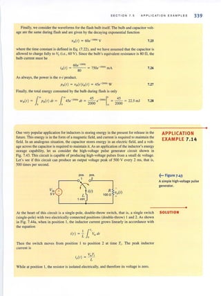
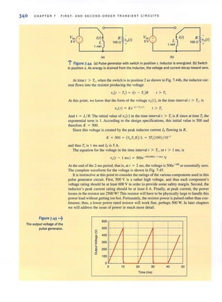
![SEC TI ON 7.5 APPLICATION EXAM PLE S 341
A hean pacemaker circuit is shown in Fig. 7.46. The SCR (silicon-controlled rectifier) is a
solid-state device that has two distinct modes of operation. When the voltage across the SCR
is increasing but less than 5 V, the SCR behaves like an open circuit, as shown in Fig. 7.47a.
Once the voltage across the SCR reaches 5 V, the device functions like a current source, as
shown in Fig. 7.47b. This behavior will continue as long as the SCR voltage remains above
0.2 V. At this voltage, the SCR shuts off and again becomes an open circuit.
Assume that at I ; 0, ve(l) is 0 V and the I-,...F capacitor begins to charge toward the
6-V source voltage. Find the resistor value such that vetl) will equal 5 V (the SCR firing
voltage) at I s. At t ; I s, the SCR fires and begins discharging the capacitor. Find the time
required for ve(l ) to drop from 5 V to 0.2 V. Finally, plot ve(l) for the three cycles.
V = 6V ~
seR ..
(a)
I
I
R
C
1 " F
+
vC(t)
seR . .
(b)
seR
APPLICATION
EXAMPLE 7.1 5
~... Figure 7.46
Heart pacemaker equivalent
circuit.
~... Figure 7.47
Equivalent circuits for
silicon-controlled rectifer.
•
For I < 1 s, the equivalent circuit for the pacemaker is shown in Fig. 7.48. As indicated SOLUTION
earlier, the capacitor voltage has the form
vdl) ; 6 - 6e-'IRC V
A voltage of 0.2 V occurs at
I, ; 0.034RC
whereas a voltage of 5 V occurs at
I, ; 1.792RC
We desire that I, - I, ; 1s. Therefore,
I, - I, ; 1.758RC ; I s
and
RC ; 0.569 sand R ; 569 kn
R
+
C
V = 6V f~____l_"F_][~VC_(_I)__~J
~... Figure 7.48
Pacemaker equivalent
network during capacitor
charge cycle.
•](https://image.slidesharecdn.com/basicengineeringcircuitanalysis9thirwin-160630150938/85/Basic-engineering-circuit-analysis-9th-irwin-363-320.jpg?cb=1719934140)
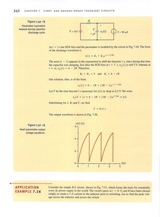
![SE CTIO N 7. 5 AP PLI CAT ION E X A M PLE S
We begin the analysis with an expression for the inductor current. At { ~ 0, the inductor cur- SOLUTION
rent is I A. At { ~ 00, the current is O. The time constant is simply L/ R, but when the switch
is open, R is infinite and the time constant is zero! As a result, the inductor current is
7.29
where a is infinite. The resulting inductor voltage is
7.30
R
1 n
•
343
+
+
At ( = 0, the peak inductor voltage is negative infinity! This voltage level is caused by the VS +
attempt to disrupt the inductor current instantaneously, driving di/ dt through the roof. 1 V
Employing KYL, the peak switch voltage must be positive infi nity (give or take the supply
voltage). This phenomenon is called inductive kick, and it is the nemesis of power supply
designers.
{ = 0 Vswitch
Given this situation, we naturally look for a way to reduce th is excessive voltage and,
more importantly, predict and control it. Let's look at what we have and what we know. We ...:-..
have a transient voltage that grows very quickly without bound. We also have an initial CUf- : Figure 7.51
rent in the inductor that must go somewhere. We know that capacitor voltages cannot The switched inductor
change quickly and resistors consume energy. Therefore, let's put an RC network around network at the heart of
the switch, as shown in Fig. 7.52, and examine the performance that results from this modern power supplies.
change.
R
1 n
+
L
vdr)100 ~H
Vs id r)
+
1 V
+ C
r = 0
Vswitch
R
The addition of the RC network yields a series circuit. We need the characteristic equa-
tion of this series RLC network when the switch is open. From Eq. (7. 15), we know that the
characteristic equation for the series RLC circuit is
, 2 ' [R + I] Ir + 2'woS + Wo = r + - L- S + LC = 0 7.31
To retain some switching speed, we will somewhat arbitrarily choose a critically damped
system where ~ ~ I and Wo ~ 10' rad/ s. This choice for Wo should allow the system to sta-
bilize in a few microseconds. From Eq. (7.31) we can now write expressions for C and R.
, 12 I I
w- = 10 =-~--
o LC IO-'C
, R + I R + I
2Ywo ~ 2 X 10 = - - = - -, L 10-' 7.32
Solving these equations yields the parameter values C ~ 10 nF and R ~ 199 fl. Now we
can focus on the peak switch voltage. When the switch opens, the inductor current, set at
1A by the de source and the I-fl resistor, flows through the RC circuit. Since the capacitor
was previously discharged by the closed switch, its voltage cannot change immediately and
~... Figure 7.52
Conversion of a switched
inductor circuit to an RLC
network in an attempt to
control inductive kick.](https://image.slidesharecdn.com/basicengineeringcircuitanalysis9thirwin-160630150938/85/Basic-engineering-circuit-analysis-9th-irwin-365-320.jpg?cb=1719934140)
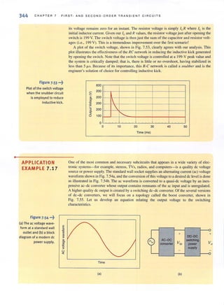
![SEC TI O N 7. 5 APPLICATION EXAMPLES 345
52 .~... Figure 7.55
+ VL(I) _
The boost converter with
+
switch settings for time
intervals (a) to, and (b) toff .
Vin -=- C R Vo
5 1
(a)
+ VL(r) _
-iL(I) +
Vjn -=- C R Vo
(b)
•
Consider the boost converter in Fig. 7.55a, where switch I (S I) is closed and S2 is open for SOLUTION
a time interval ton . This isolates the inductor from the capacitor,creating two subcircuits that
can be analyzed independently. Note that during 10
, the inductor current and stored energy
are increasing while at the output node, the capacitor voltage discharges exponentially into
the load. If the capacitor's time constant (T = RC) is large, then the output voltage will
decrease slowly. Thus, during I on energy is stored in the inductor and the capacitor provides
energy to the load.
Next, we change both switch positions so that S I is open and S2 is closed for a time
interval t orf' as seen in Fig. 7.55b. Since the inductor current cannot change
instantaneously, current flows into the capacitor and the load, recharging the capacitor.
During toff the energy that was added to the inductor during ton is used to recharge the
capacitor and drive the load. When toff has elapsed, the cycle is repeated.
Note that the energy added to the inductor during'on must go to the capacitor and load
during 'off; otherwise, the inductor energy would increase to the point that the inductor
would fail. This requires that the energy stored in the inductor must be the same at the end
of each switching cycle. Recalling that the inductor energy is related to the current by
wet) = iLi2
(t)
we can state that the inductor current must also be the same at the end of each switching
cycle, as shown in Fig. 7.56. The inductor current during Ion and toff can be written as
I 1'~ I 1'~ [V, ]iL{t) = ~ vL(t) dt = - ViII dt = ~ tOil + 10
L 0 L 0 L
0 < t < tOil
[",'-V"]L toff + 10 ton < I < toff 7.33
where lois the initial current at the beginning of each switching cycle. If the inductor
current is the same at the beginning and end of each switching cycle, then the integrals in
Eg. (7.33) must sum to zero. Or
V;,to, = (V, - "',)toff ~ (V, - ",,)(T - too)](https://image.slidesharecdn.com/basicengineeringcircuitanalysis9thirwin-160630150938/85/Basic-engineering-circuit-analysis-9th-irwin-367-320.jpg?cb=1719934140)
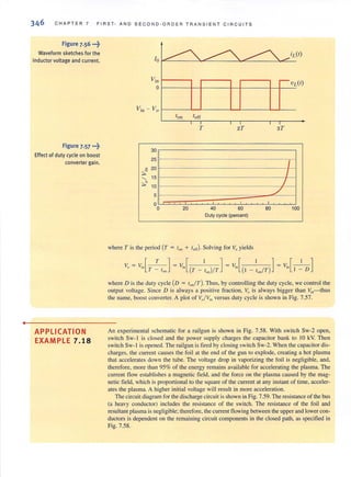
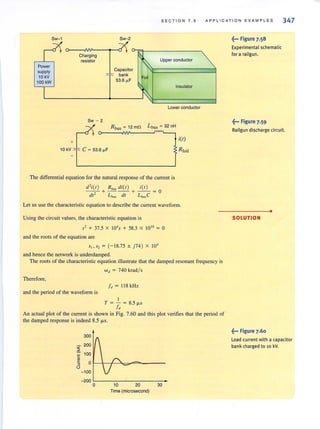
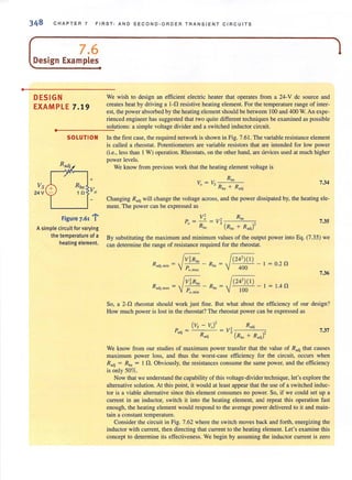
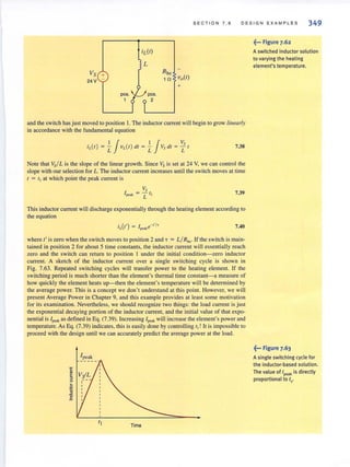
![S ECT I ON 7.6 DE SI G N E X AMP L E S
Vs +
RS
+
v,- "R'_1C'
(a) (b)
l' Figure 7.65 The circuit in Fig. 7.64b at t ~ a just after the switch has moved. (b) The same circuit at t ~ 00.
At exactly, = I', the output voltage is its original value, Vo(O ) plus a VQ' Substituting this
condition into Eq. (7.43) yields
which can be reduced to the expression
6. Vs - a vo = 6. Vs e-t'IRsC" 7.44
Notice that the value of Co depends not on the input and output voltages, but rather on the
changes in those voltages! This makes Eq. (7.44) very versatile indeed. A simple algebraic
manipulation of Eq. (7.44) yields the design equation for CD'
"CD ~ - --;--'-:-c-:--:;-
Rs ln[ Ll.V, ]
Ll.Vs - Ll.V,
7.45
Examining this expression, we see that Co is directl y related to t' and inversely related to
Rs. If t' doubles or if Rs is halved, then Co will double as well. This result is not very sur-
prising. The dependence on the voltage changes is more complex. Lei us isolate this t.erm
and express it as
f~--=---~
[
Ll.Vs ]In
/l Vs - /l v"
7.46
Figure 7.66 shows a plot of this term versus the ratio aVol.6.Vs. Note that for very small
6. Vo (Le., a large degree of decoupling) this term is very large. Since this term is multi-
plied with t' in Eq. (7.45), we find that the price for excellent decoupling is a very large
capacitance.
100 r-- --,-- - - , - - --,--- ,
~ 75 ~--_+---~---~---1
E
2.2 50 Hr------~-------4--------+_-------1
E
.c
~ 25 r------~-------4--------+_------4
§" "O~~~==~~--~--~o 0.25 0.5 0.75
/lV"ILl.VS
~••• Figure 7.66
A plot of the function, f,
versus 6 Vol tl Vs.
351](https://image.slidesharecdn.com/basicengineeringcircuitanalysis9thirwin-160630150938/85/Basic-engineering-circuit-analysis-9th-irwin-373-320.jpg?cb=1719934140)
![•
354 C H APTER 7 FIRST· AND S E COND · ORDER TRANSIE NT CIRC UIT S
DESIGN
EXAMPLE 7.22
•
3000
iL(t) we should reduce sl " Hence, let us choose SI = I. Since 51 + '"2 must equal 20,
52 = 19. Under these conditions
I I
C ~ - - ~ -;::--::-c-;'--;-;-c:::- ~ 263 mF
LsIs, (0.2)( 1)( 19)
and
Thus, the current is
iL( r) ~ 3.33[e-' - e-"' ]A
which is shown in Fig. 7.68b. At 100 ms the current is 2.52 A. Also, at r ~ Ll s, the cur-
rent is 1.11 A-above the I-A requirement. Therefore, the choice of C ~ 263 mF meets all
starter specifications.
A defibrillator is a device that is used to stop heart fibril1ations---erratic uncoordinated
quivering of the heart muscle fibers- by delivering an electric shock to the heart. The Lawn
detibrillator was developed by Dr. Bernard Lown in 1962. Its key feature, shown in Fig. 7.69a,
is its voltage waveform. A simplified circuit diagram that is capable of producing the Lown
waveform is shown in Fig. 7.69b. Let us find the necessary values for the inducLOr and
capacitor.
o 10
Time (milliseconds)
(a) (b)
L i(t)
.""--
R ~ 500
patient
+
l ' Figure 7.69 l awn defibrillator waveform and simplified circuit. Reprinted with permission from
John Wiley & Sons, Inc., Introduction to Biomedical Equipment Technology.
SOLUTION Since the Lown waveform is oscillatory in nature, we know that the circuit is underdamped
(~ < I) and Ihe voltage applied to the patient is of the form
v,,(r) ~ Kle-(w"'sin[wr J
where
and
I
w ~ --
" VIT](https://image.slidesharecdn.com/basicengineeringcircuitanalysis9thirwin-160630150938/85/Basic-engineering-circuit-analysis-9th-irwin-376-320.jpg?cb=1719934140)
![•
CHAPTER 7 FIRST- AND SECOND-ORDER TR ANS IENT CIRCUITS
SUMMARY
First-Order Circuits
• An RC or RL transient circuit is said to be first order if it
contains only a single capacitor or single inductor. The
voltage or current anywhere in the network can be obtained
by solving a first-order differential equation.
• The form of a first-order differential equation with a con-
stant forcing function is
dX(I) X(I)
- - + - - =A
dl T
and the solution is
where A T is referred to as the steady-state solution and T is
called the time constant.
• The function e- 1/1 decays to a value that is less than 1%of
its initial value after a period of ST. Therefore, the time
constant, T, determines the time required for the circuit to
reach steady state.
• The time constant for an RC circuit is RThC and for an RL
circuit is L/RTh , where RTh is the Thevenin equivalent
resistance looking into the circuit at the terminals of the
storage element (i.e., capacitor or inductor).
• The two approaches proposed for solving first-order
transient circuits are the differential equation approach and
the step-by-step method. In the former case, the differential
equation that describes the dynamic behavior of the circuit
is solved to determine the desired solution. In the latter
case, the initial conditions and the steady-state value of the
voltage across the capacitor or current in the inductor are
used in conjunction with the circuit's time constant and the
known form of the desired variable to obtain a solution.
PROBLEMS
7.1 Use the differential equation approach to find i(t) for
1 > 0 in the network in Fig. P7. 1.
( = 0
12V +
2H
Figure Pl.l
60
;(1)
60
• The response of a first-order transient circuit to an input
pulse can be obtained by treating the pulse as a combina-
tion of two step-function inputs.
Second-Order Circuits
• The voltage or current in an RLC transient circuit can be
described by a constant coefficient differential equation
of the fonn
d'x(l) dX(I) ,
--,- + n wo- - + WQX(I) = j(l)
dr df
where f(t) is the network forcing function.
• The characteristic equation for a second-order circuit is
52 + 2'wos + w5= 0, where' is the damping ratio and
Wo is the undamped natural frequency.
• If the two roots of the characteristic equation are
• real and unequal, then , > I and the network response is
overdamped
• real and equal, then , = I and the network response is
critically damped
• complex conjugates, then, < I and the network
response is underdamped
• The three types of damping together with the corresponding
network response are as follows:
1. O verdamped:
x(t) = K le-((Wo-wo'-"N)t + K2
e-« WQ+WD'-"N)t
2. Critically damped: X(f) = Ble-cwol + B2te-,wol
3. Underdamped: x{t) = e-o-t(A I COS Wti f + A2 sinwdI),
where 0- = 'wo and W d = Wo ~
• Two initial conditions are required to derive the two
unknown coefficients in the network response equations.
7.2 Use the differential equation approach to find io(f ) for
t > 0 in the network in Fig. P7.2.
4 kO 1 kO
t ~ 0
2 kO 4 rnA 2 kO 300 ~F
Figure P].2](https://image.slidesharecdn.com/basicengineeringcircuitanalysis9thirwin-160630150938/85/Basic-engineering-circuit-analysis-9th-irwin-378-320.jpg?cb=1719934140)
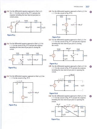
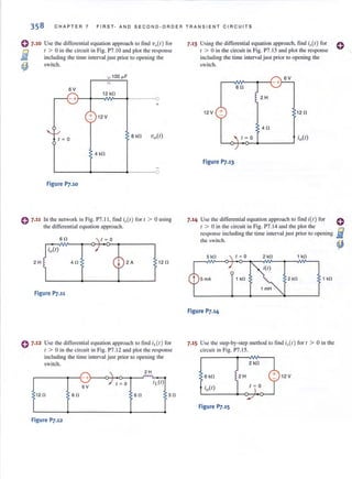
![e 7·16 Usc the step-by-step technique to find (,(I ) for 1 > 0 in
the network in Fig. P7.16.
2 kO 4 kfl
12 V 200 ~ F 6 kO
/ ~ 0
Figure P7.16
7.17 Find io(l) for t > 0 in the network in Fig. 7.17 using the
step-by-step method.
1 - 0
~/
4fl
6A
t 12 fl 6fl !1
t
H
iiI)
Figure P].17
PROBLEMS 359
7.18 Use the step-by-step method to lind i,,(/) for / > [) in
the circuit in Fig. P7.1 8.
6fl
60 24V
Figure P7.18
7.19 Use the step-by-step method to lind io(l) for / > 0 in
the circuit in Fig. P7.19.
200 ~F
12 kO 12 kfl
Figure P].19
o
o
7.20 Find 'vo(t) for ( > 0 in the network in Fig. P7.20 lIsing the step-by-step
technique.
3 kfl 3kfl
24 V
1 ~ 0
Figure P7.20
e 7.21 Use the step-by-step technique 10 find i)/) for I > 0 in
the network in Fig. P7.21.
4 kfl 4 kfl
4 kO 4 kfl 200 ~F
Figure P7.21
200 ~ F
0
+
6 kO 2 kfl Vo(l)
0
7·22 Use the step-by-step method to find 'V,,(r) for t > 0 in e
the network in Fig. P7.22.
/ ~ 0
6kfl
100 ~F
Figure P7.22](https://image.slidesharecdn.com/basicengineeringcircuitanalysis9thirwin-160630150938/85/Basic-engineering-circuit-analysis-9th-irwin-381-320.jpg?cb=1719934140)
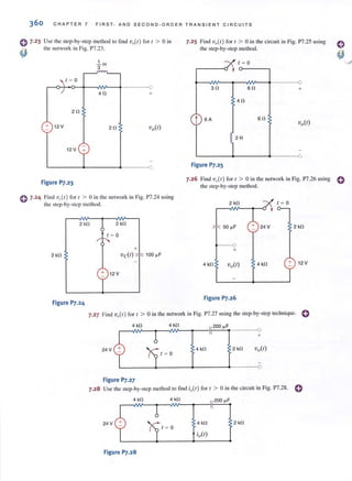
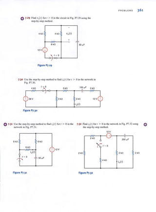
![362 CHAPTER 7 FIRST - A N D S E CO ND - OR DE R TRANSIENT CIRCUIT S
o 7·33 Use the Slep·by·step technique to lind 'V,,(I ) for 1 > 0 in
the circuit in Fig. P7.33.
+
6 kn 50 ~F ' f< 6 kn 'Vn(I)
6 kn -
0
1 ~ 0
~
:--..
6 kn
CP 12V
Figure P7.33
0 7.34 Use the step·by·step technique to find i,,(I) for 1 > 0 in
7.)6 The switch in the circliit in Fig. P7.36 is moved at I = O. Iii
Find i,J/) for I > 0 using the step-by-step technique. ..;;..,
t= 0
4 kn 2 kn 6kn
30V 12 kn 12 mH 12 V
Figure P7.36
7.37 The switch in the circuit in Fig. P7.37 is moved at t = o.
Find iR(t ) for t > 0 using the step-by-step technique.
t = 0
5 kn 3 kn 3 kn
20V 6 kn 5mH
12V
~ the network in Fig. P7.34. Figure P7.37
4 kn 100 ~F 2kn
2 kn
2 kn 12 kn 4V
Figure P7.34
0 7.35 Find vir) for t > 0 in the network in Fig. P7.35 using
the step-by-step technique.
~
+
2 n 2n
2 H
1 ~ 0
".,------<0
Figure P7.35
7.38 The switch in the circuit in Fig. P7.38 is moved at 1 = O.
Find ;,,(/ ) for 1 > 0 using the step-by-step technique.
1= 0
2 kn
24V + 12 kn
20 mH
Figure P].38
7.39 The switch in the circlLit in Fig. P7.39 is opened at f = O.
Find 1)0(/) for ( > 0 lIsing the step-by-step technique.
16kn 10~F
12 V
-+
+ 16 kn
24 V
t=0 + 4kn
vo(t) 12 kn
Figure P7.39](https://image.slidesharecdn.com/basicengineeringcircuitanalysis9thirwin-160630150938/85/Basic-engineering-circuit-analysis-9th-irwin-384-320.jpg?cb=1719934140)
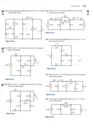
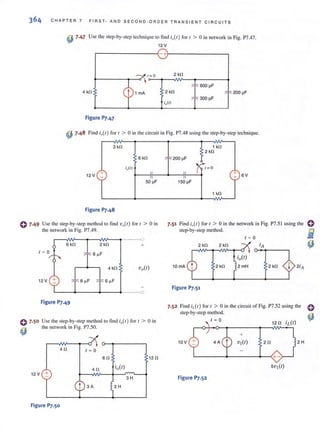
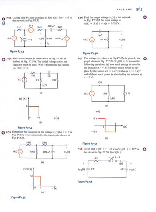
![366 CHAPTER 7 FIRST · AND S E COND·ORD ER TRANSIENT CIRCUIT S
o 7·59 The switch in the circuit in Fig. P7.59 isclosed at t = O.
If i,(O-) = 2 A. determine i,(o+), v.(o+). and
i,(1 = 00) .
1 = 0
+
2H 3H
Figure 1'].59
o 7.60 In the network in Fig. P7.60 find i(l) for I > O. If
V"I(D-) = - lOY, calculate vdD- ).
i(l)
Vcl (I)
+ -
D3~+
0.6 F VC2(t)
Figure 1'].60
0 7.61 In the circuit in Fig. P7.6 1, 'UN(t) = IOOe-~uol V for
I < O. Find V.( I ) for I > O.
1 = 0
+
250 1000 VI/(t) L
Figure P7.61
e 7·62 The switch.in the ci~cui t in Fig. P7.62 has been closed
~ for a long time and IS opened at f = O. If
'jP ·v,.(t) = 20 - 8e...·05
' Y. find R,. R" and C.
+
R2
t 2A R, C O'
'" vcCt)
1 = 0
,,- ('
Figure P7.62
7·63 Given that i(l) = 13.33e-' - 8.33e-o·" A for I > 0 in
the network in Fig. P7.63. find the following:
(a) v,(O), (b) V,(I = I s), and (c) the capacitance C.
vcCt)+ -
C
20
Figure 1'].63
7.64 Given that itt) = 2.5 + l.5e-" A for I > 0 in the
circuit in Fig. P7.64, find RI• R2• and L.
L
Figure P7.64
7.65 For the circuit in Fig. P7.65, choose RIo R2• and L such
that
V,,( I ) = -20 e-lIt, Y
and the current i1 never exceeds I A .
R,
10V + o----....--<J
1=0 +
Figure P7.65](https://image.slidesharecdn.com/basicengineeringcircuitanalysis9thirwin-160630150938/85/Basic-engineering-circuit-analysis-9th-irwin-388-320.jpg?cb=1719934140)
![PROBLEMS 367
7.66 For the network in Fig. P7.66, choose C so the lime constant will be 120 I-LS for
I > O.
t= 0
4 kO
Vs 23 kO 18 kO
Figure p].66
7.67 The differential equation that describes the current io(l)
in a network is
d'io(t) di,,{l )
--,- + 6- - + 4io(l ) = 0
dr dt
Find (a) the characteristic equation of the network, (b)
the network 's natural frequencies, and (c) the expression
fori,,(I).
7.68 The terminal current in a network is described by the
equation
,I'io(l) di,(I)
--,- + 8- - + 16i,,{l) = 0
dr dl
Find (a) the characteristic equation of the network, (b)
the network's natural frequencies, and (c) the equation
for i,,{I).
7.69 The voltage 'VI(t) in a network is defined by the equation
d'v,(l) dv,(t)
- -,- + 4- - + 5v,(t) = 0
dr dr
Find (a) the characteristic equation of the network, (b)
the circuit's natural frequencies, and (c) the expression
for v,(t) .
7.70 The output voltage of a circuit is described by the differ-
ential equation
d'vo( I) dvo( I)
--,- + 8- - + 10v.,{l) = 0
dt' dt
Find (a) the characteristic equation of the circuit, (b) the
network's natural frequencies, and (c) the equation for
V,,(I).
C 7·71 The voltage vl{t) in a network is defined by the equulion
d'1),(I ) [ dV,(I)]
--,- + 2 - - + 5v,(1) = 0
dl - dl
Find
(a) the characteristic equation of the network.
(b) the circuit's natural frequencies.
(el the expression for V,( I).
2kO
C
0
+
7 kO Vo(I)
0
7.72 The parameters for a parallel RLC circuit are R = I n ,
L = 1/ 2 H. and C = 1/ 2 F. Determine the type of
damping exhibited by the circuit.
7.73 A series RLC circuit contains a resistor of R = 2 nand 0
a capacitor C = 1/ 2 F. Select the value of the induclOr
so that the circuit is critically damped.
7.74 A parallel RLC circuit contains a resistor I? = I nand 0
an inductor L = 2H. Select the value of the capacitor so
that the circuit iscritically damped.
7.75 For the underdamped circuit shown in Fig. P7.75, 0
determine the voltage v( t) if the initial conditions on the
storage clements arc iJO) I A and v,(O) = 10 V.
2H
I
Figure P].75
+ +
V(t) 50 1 ,~ vc(O)
40 F
7.76 In the critically damped circuit shown in Fig. P7.76. the 0
initial conditions on the storage clements ure i,.(O) = 2 A
and v,(O) = 5 V. Determine the voltage v(t ).
+ +
vc(o) 'r 001 F v(t) 100
r
Figure P7.76
7.77 Find v,.{t) for t > 0 in the circuit in Fig. P7.77. ()
t = 0
+
1 A 80 0.04 F
Figure P7.77](https://image.slidesharecdn.com/basicengineeringcircuitanalysis9thirwin-160630150938/85/Basic-engineering-circuit-analysis-9th-irwin-389-320.jpg?cb=1719934140)
![PROBLEMS 369
0 7.84 Find vQ(t) for [ > 0 in the circuit in Fig. P7.S4 and plOi the response includi ng the lime interval
just prior to closing the switch.
1.5 A 40
Figure P7.84
80
so
~ H
8
o 7.8 5 The switch in the circuit in Fig. P7.85 has been closed
D for a long time and is opened at I = O. Find ;(1) for
Ji:! / > o.
/ ~ 0
50 50
50
i(/)
+ 20 V 0.04 F
1 H
10 V
Figure p].8S
e 7.86 The switch in (ile circuit in Fig P7.86 has been closed
for a long time and is opened at I = O. Find ;(t) for
/ > o.
so
12V +
i(/)
1.25 H
Figure P7.86
1.50
/ ~ 0
0.1 F
SV
/ ~ 0
o I
.lH8
+](https://image.slidesharecdn.com/basicengineeringcircuitanalysis9thirwin-160630150938/85/Basic-engineering-circuit-analysis-9th-irwin-391-320.jpg?cb=1719934140)
![370 CHAPTER 7 FIRST · AND SECOND · ORDER TRANSIENT C I RC UITS
~ 7.87 Find V,,(I) fo r I > 0 in the circuit in Fig. P7.87 and plot the
response including the time interval just prior to moving the
switch.
7.88 Design a parallel IILe eircllil with II ~ I ki1 0
that h<ls the characteristic equation
S2 + 4 X 10⁷
S + 4 X 1014
= 0
I = 0 2.5 mH 8 kfl 7.89 Design a parallel RLC circuit with R ~ J k!1 0
that has the characteristic equation
1 kfl
6 kfl
Figure p].87
----<: 6 kfl
+
.'1
2
+ 4 X I07s + 3 X 1014
= 0
4 kn t
3mA
7.90 For the nelwork shown in Fig. P7.90, use PSPICE to plot V,,(I )
over a 10-sec interval starting at ( = 0 using a IOO-ms step size.
12 V
r-~~---~I-{- +'~-4~~~--~------4~
4fl 6 2 0
1 = 0
2H 1F ::f': 40
30
L-______~------+_------4-----~O
Figure p].90
7.91 For the network in Fig. P7.91 , find i(/) for t > 0 given the 3.33-}-lF
capacitor's initial conditions listed below, and use PSPICE to plot each
current on the same graph .
(a) v,W) = 0 V
(b) ·v,.W ) = 6 V
(e) v,W) = 24V
(d) v,.W) = - 24V
18 V
Figure P].91
1 = 0
4.5 kfl
13 kfl 9kO
3 kfl
i(l)
c + 6 kfl
Vc(I)](https://image.slidesharecdn.com/basicengineeringcircuitanalysis9thirwin-160630150938/85/Basic-engineering-circuit-analysis-9th-irwin-392-320.jpg?cb=1719934140)
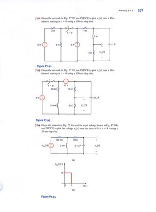
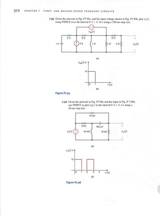
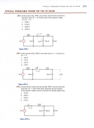
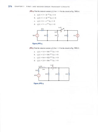

![376 CHAPTER 8 AC STEAD Y-S TATE A NAL YSIS
8.1
Sinusoids
Figure 8.1 ...j)
Plots of a sine wave as a
function of both wt and t.
[hin t]
The relationship between
frequency and period
[hin t ]
The relationship between
frequency, period. and radian
frequency
[hin t]
Phase lag defined
[hint]
In phase and out of phase
defined
Let us begin our discussion of sinusoidal functions by considering the sine wave
X(I ) = X,If sin wI 8.1
where X( 1) could represent either v{t) or ;(1). X,., is the tlmplilude, maximum vallie or peak
value, w is the radian or tlllgular!requellcy, and wI is the argument of the sine function. A
plot of the fu nction in Eq. (8. 1) as a function of its argument is shown in Fig. 8. la. Obviously.
the function repeals itself every 21T radians. This condition is described mathematically as
x(wI + 2'IT) = x(WI) or in general for period T as
X(W{I + Tl] = X{WI)
meani ng that the function has the same value at time t + T as it does at time I.
X(WI)
XM
(a) (b)
8.2
The waveform can also be plotted as a function of time, as shown in Fig. 8. 1b. Note thal
this function goes th rough one period every T seconds, or in other words, in J second
it goes through 1/1' periods or cycles. The number of cycles per second, called Hertz, is the
frequency J, where
I
J= -T
Now since wT = 27T, as shown in Fig. 8. 1a, we find that
2'IT
W = - = 2'ITJ
T
8.3
8.4
which is, of course, the general relationship among period in seconds, frequency in Hertz, and
radian frequency.
Now that we have discussed some of the basic properties of a sine wave. let us consider
the following general expression for a sinusoidal function:
X{I) = X" sin {wl + 9) 8.5
In this case (WI + 8) is the argument of the sine function, and 0 is called the phase (Ingle.
A plot of this function is shown in Fig. 8.2, together with the original function in Eq. (8. 1)
for comparison. Because of the presence of the phase angle, any point on the waveform
XMsin(wI + 0) occurs 0 radians earlier in time than the corresponding point on the wavc-
foml X", sin wI. Therefore, we say that X", sin wI lags X", sin (WI + 9) by 9 radians. In the
more general situation, if
X,{ I) = X" , sin {wl + 0)
and
-,,{I) = X"" sin {WI + <1»](https://image.slidesharecdn.com/basicengineeringcircuitanalysis9thirwin-160630150938/85/Basic-engineering-circuit-analysis-9th-irwin-398-320.jpg?cb=1719934140)
![SECTION 8.1 S INUS O IDS 377
X(WI)
wI
then X,(I) leads X,( I) by 0 - 4' radians and X,(I) lags X,(I) by e - <p radians. If e = <p, the
waveforms are identical and the functions are said to be ill phase. If e *- 4>,the functions are
out ofphase.
The phase angle is normal.ly expressed in degrees rather than radians. Therefore, at this
point we will simply stale that we will use the two forms interchangeably; thai is,
X(I) = x Msin ( wI +~) = X"sin(wl + 90°) S.6
Rigorously speaking, since wt is in radians, the phase angle should be as well. However, it is
common practice and convenient to use degrees for phase; therefore, that will be our practice
in this text.
In addition, it should be noted that adding to the argument integer multiples of either 21T
radians or 3600
does not change the original function. This can easily be shown mathemati-
cally but is visibly evident when examining the waveform, as shown in Fig. 8.2.
Although our ctiscussion has centered on the sine function, we could just as easily have
used the cosine function, since the two waveforms differ only by a phase angle; that is,
coswr = Sin ( wI + %) 8.7
sinwt = cos( wf ~ %) 8.8
We are often interested in the phase difference between two sinusoidal fu nctions. Three
conditions must be salisfied before we can determine the phase difference: ( I ) the
frequency of both sinusoids must be the same, (2) the amplitude of both sinusoids must be
positive, and (3) both sinusoids must be written as sine waves or cosine waves. Once
in this format, the phase angle between the functions can be computed as outlined
previously. Two other trigonometric identities that normally prove useful in phase angle
determination are:
-COS ( WI ) = COS(WI ± ISOO) 8.9
-sin (wI ) = sin (wl ± ISOO) 8.10
Finally, the angle-sum and angle-difference relationships for sines and cosines may be
useful in the manipulation of sinusoidal functions. These relations are
sin(a + 13) = sinn cos 13 + cosasinl3
cos(a + 1» = cosacosl> - sin "sin ~
8.1l
sin (a - 1» = sin" cos ~ - cosasin~
cos(a ~ 13) = cosacosl3 + sin asin l3
.~••• Figure 8.2
Graphical illustration of
XMsin(wt + 0) leading
XM sin wt by eradians.
[hint]
Phase lead graphically
illustrated
[hint]
Avery important point
[hin t]
Some trigonometric identities
that are useful in phase angle
calculations](https://image.slidesharecdn.com/basicengineeringcircuitanalysis9thirwin-160630150938/85/Basic-engineering-circuit-analysis-9th-irwin-399-320.jpg?cb=1719934140)
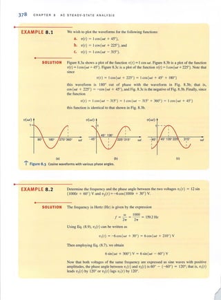
![•
CHAPTER 8 A C S TE A D Y·S TAT E A N A LY S IS
EXAMPLE 8.4
•
The real and imaginary parts of this function are each realizable. We think of this complex
forcing functionas two forcing functions, a real one and an imaginary one, and as aconsequence
of linearity, the principle of superpositionapplies and thus the current response can be writtenas
itt) = IMcos(wt + $) + j1M sin (wt + $) 8.16
where 1Mcos (wt + $ ) is the response due to VMcos wt and ji Msin (wt + $) is the response
due lO JVA! sin w!. This expression for the current containing both a real and an imaginary
term can be written via Euler's equation as
8.17
Because of the preceding relationships, we tind that ratherthan applying the forcing function
V MCOS W! and calculating the response I'I'COS(W! + (~), we can apply the complex forcing
function v,/dw1
and calculate the response IMd(wI+<J» , the real part of which is the desired
response 1Mcos (wt + $). Although this procedure may initially appear to be more compli-
cated, it is not. It is through this technique that we will convert the differential equation to an
algebraic equation that is much easier to solve.
Once again, let us determine the current in the RL circuit examined in Example 8.3.
However, rather than applying VMCOSWT we will apply V!o1 dWl.
SOLUTION The forced response will be of the form
[hint]
Summary of complex number
relationships:
x+jy =rei6
r = Vx' + y'
e = tan-l~
x
x=- (COSe
y =- rsin e
itt) = IM dl~")
where only 1Mand ¢ are unknown. Substituting Vet) and itt ) into the differential equation
for the circuit, we obtain
RI e-i(WI +W) + L!!..- (J d(w!+6») = V e'W!M ~ M At
Taking the indicated derivative. we obtain
RIMel'(wt+<P) + jwLI", ei(wt+4» = VM~Wf
Dividing each tenn of the equation by the common factor d"" yields
RI,IIel'6 + jwLI", el'<P = V",
which is an algebraic equation with complex coefficients. This equation can be written as
I dQ _ _ -,-V",M_
.If - R + jwL
Converting the right-hand side of the equation to exponential or polar form produces the
equation
VA! e f- tlln-l(w/./R)]
VR2 + w2L 2
(A quick refresher on complex numbers is given in the Appendix for readers who need to
sharpen their skills in this area.) The preceding form clearly indicates that the magnitude
and phase of the resulting current are
and
wL
$ = - tan- I -
R](https://image.slidesharecdn.com/basicengineeringcircuitanalysis9thirwin-160630150938/85/Basic-engineering-circuit-analysis-9th-irwin-404-320.jpg?cb=1719934140)
![S E C TI ON 8.3 PHA S ORS
However, since our actual forcing function was VMcoswr rather than VMeiwl
, our actual
response is the real part of the complex response:
itt) = I"cos(wt + <1»
WL)tan-If?
Note that this is identical to the response obtained in the previous example by solving the
differential equation for the current i(t).
Once again let us assume that the forcing fu nction for a linear network is of the form
v(t) = V"e;w,
Then every steady-state voltage or current in the network will have the same form and the
same frequency w; for example. a current i(t) will be of the form itt) = I",d(~+~)
As we proceed in our subsequent circuit analyses. we will simply note the frequency and
then drop the factor eiwJ
since it is cOlllmon to every term in the describing equations.
Dropping the term eiwl
indicates that every voltage or current can be fully described by a mag-
nitude and phase. For example, a voltage v{r) can be written in exponential form as
v(t) = V" cos(wt + 0) = Re[ V"d(~+') l 8.18
or as a complex number
v(t) = Re(V" ~ ei~) 8.19
Since we are working wi th a complex forcing function, the real pari of which is the
desired answer, and each term in the equation will contain ei"IJ, we can drop Re(-) and eiwJ
and work only with the complex number VM I.!!.: This complex representation is commonly
called a phasor. As a distinguishing feature, phasors will be wri tten in boldface type. In a
completely identical manner a voltage v(t) = V"cos(wt + 9) = Re[ V", d(~ +O) l and a
current i(f) = I",cos(wr + (~) = Re[/", ei(WI+<!»] are written in phasor notation as
V = V"'~ and I = I",/!i..respectively. Note that it is common practice to express pha-
sors with positive magnitudes.
Again, we consider the RL circuit in Example 8.3. Let us use phasors to determine the
expression for the current.
The differential equation is
diet)
L -~ + Ri(l) = V" cos wt
dt
The forcing funct ion can be replaced by a complex forcing function that is written as vd~
with phasor V = V",I!!.. Similarly. the forced response component of the current itt) can
be replaced by a complex function that is written as Id~ with phasor I = I", /!i..From our
previous discussions we recall that the solution of the differential equation is the real part
of this current.
8.3
Phasors
[hin tj
If v(1) ~ V. (05 (wl + 0) and
i(l) ~ I. (05 (wl + <1» . then
in phasor notation
v~ V. 1.2.
and
EXAMPLE 8.5
•
SOLUTION
•](https://image.slidesharecdn.com/basicengineeringcircuitanalysis9thirwin-160630150938/85/Basic-engineering-circuit-analysis-9th-irwin-405-320.jpg?cb=1719934140)
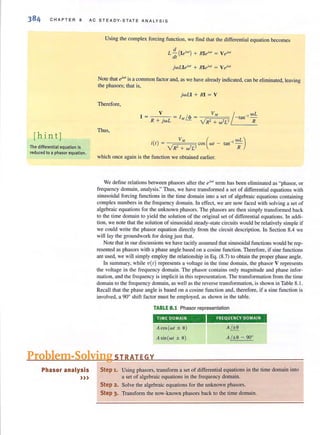
![SEC T ION 8.4 PHASOR R EL ATIONSHIPS FOR CIRC UI T EL E MEN T S
However. if a network contains only sine sources. lhere is 110 need to performlhe 90° shifl.
We simply perform the normal phasor analysis, and then the imagi1lary part of the time-
varying complex solution is the desired response. Simply put, cosine sources generate a
cosine response. and sine sources generate a sine response.
l.earning ASS ESS MEN IS
E8.3 Convert the following voltage functions to phasors.
V,(I) = 12 cos (3771 - 425°) V
'U,(I) = 18 sin (25131 + 4,2°) V
ANSWER: V, = 12 /-425° V;
V, = 18 /- 85,8° V,
E8.4 Convert the following phasors to the time domain if the frequency is 400 Hz. ANSWER:
V, = 10 / 20° V
V, = 12 / -60° V
V,(I) = IO cos (800"1 + 20°) V;
V,(I) = 12 cos (800,,1 - 60°) V,
As we proceed in our development of the techniques required to analyze circuits in the Sillll-
soidal steady state, we are now in a position to establish the phasor relationships between
voltage and current for the three passive elements R, L, and C.
tn the case of a resistor as shown in Fig. 8.6a, the voltage-current relationship is known to be
V(I ) = Ri(l ) 8,20
Applying the complex voltage V,IleAl<.>'+tlr) results in the complex current I MeAl<.>'+oJ, and there-
fore Eq, (8.20) becomes
v eA"'+o,,) = RI .,Aw,+o,)
M .II
which reduces to
v",ei" = RIMei°'
Equation (8,2 1) can be written in phasor form as
V = RI
where
8,21
8.22
From Eq. (8.2 1) we see thnt ell = 0; and thus the current and voltage for this circuit are in
phase.
Historically, complex numbers have been represented as points on a graph in which rhe
x-axis represents the real axis and the y-axis the imaginary axis. The line segment connect-
ing the origin with the point provides:l convenient representation of the magnitude and angle
when the complex number is written in a polar form. A review of the Appendix will indicate
how these complex numbers or line segments can be added, subtracted, and so on. Since
phasors are complex numbers, it is convenient to represent the phasor voltage and current
graphically as line segments. A plot of the line segments representing the phasors is called a
phasor diagram. This pictorial representation of phasors provides immediate information on
the relative magnitude of one phasor with another, the angle between two phasors, and the
relati ve position of one phasor with respect to another (i.e., leading or laggi ng). A phasor
diagram and the sinusoidal wavefonns for the resistor are shown in Figs. 8.6c and d, res-
pectively. A phasor diagram will be drawn for each of the other circuit elements in the
remai nder of this section.
8.4
Phasor
ReLationships
for Circuit
Elements
[hint]
Current and voltage are in
phase.](https://image.slidesharecdn.com/basicengineeringcircuitanalysis9thirwin-160630150938/85/Basic-engineering-circuit-analysis-9th-irwin-407-320.jpg?cb=1719934140)
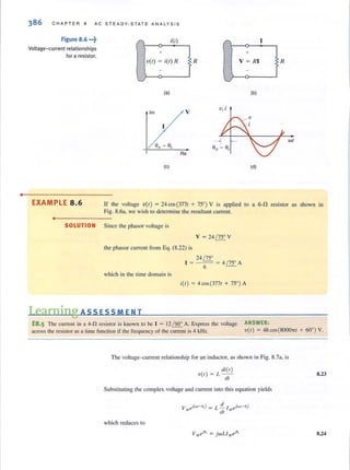
![SECTION 8 . 4 PHASOR RE LATIONSH I PS FOR CIRCUIT ELEMENTS
i(l) ,..,
+ +
( ) L
di(t)
v r =: dr L V ; jwLl )L
...,
(a) (b)
1m V(I), i(l)
wI
(c) (d)
Equation (8.24) in phasor notalion is
v ; jwLI 8.25
Note that the differential equation in the time domain (8.23) has been converted to an alge-
braic equation with complex coefficients in the frequency domain. This relationship is
shown in Fig. 8.7b. Since the imaginary operator j ; l eflO" ; 1/ 90' ; vCf, Eq. (8.24)
can be written as
8.26
Therefore, the voltage and current are 90° out ofplwse, and in panicuiar [he voltage leadsthe
current by 90° or the current lags the voltage by 90°. The phasor diagram and the sinusoidal
waveforms for the inductor circuit are shown in Figs. 8.7c and d, respectively.
The voltage V( I ) ; 12cos(3771 + 20' ) V is applied to a 20-mH inductor as shown in
Fig. 8.7a. Find the resullant current.
The phasor current is
or
V 12 / 20'
I ; - ; --:-=;:=:,
jwL wL / 90'
12/ 20°
(377)(20 x 10 ') / 90°
1.59 / -70° A
;(1); 1.59cos(3771-700) A
.~... Figure 8.7
Voltage-current relationships
for an inductor.
[hin t ]
The derivative process yields
a frequency-dependent
function.
[hint]
The voltage leads the current
or the current lags the
voltage.
EXAMPLE 8.7
•
SOLUTION
[hint]
•](https://image.slidesharecdn.com/basicengineeringcircuitanalysis9thirwin-160630150938/85/Basic-engineering-circuit-analysis-9th-irwin-409-320.jpg?cb=1719934140)
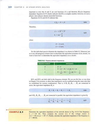
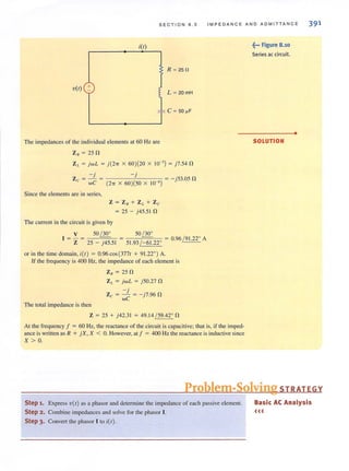
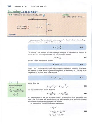
![SEC TI ON 8.5 IMPEDANCE AND ADMITTANCE
Once again, since KCL and KVL are valid in the frequency domain, we can show, using
the same approach outlined in Chapter 2 for conductance in resistive circuits, that the rules
for combining admittances are the same as those for combining conductances; that is, if
YI , Y2 , Y3, ... , Yn are connected in parallel, the equivalent admittance is
8.45
and if YI , Y2 • ... , Y,rare connected in series, the equivalent admittance is
8.46
393
Calculate the equivalent admittance Ypfor the network in Fig. 8.1 1 and use it to determine EXAM PLE 8.10
the current I ifVs ~ 60(45' V.
I ~... Figure 8.11
Vs
From Fig. 8.11 we note that
1 I
YR ~ - ~ - 5
ZR 2
1 - j
YL ~ - ~ - 5
Z L 4
Therefore,
and hence,
I ~ YpVs
~ G-j±)(60 /45' )
~ 33.5/ 18.43' A
Learning AS S ESSM E N T
E8.9 Find the current I in the network in Fig. E8.9.
I
Figure E8.9
Zc =- j1 n ZR =4 n
An example parallel
circuit.
•
SOLUTION
[hint]
Admittances add in
parallel.
ANSWER: I ~ 9.01 /53.7' A.
•](https://image.slidesharecdn.com/basicengineeringcircuitanalysis9thirwin-160630150938/85/Basic-engineering-circuit-analysis-9th-irwin-415-320.jpg?cb=1719934140)
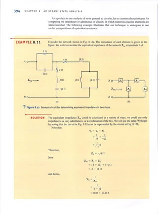
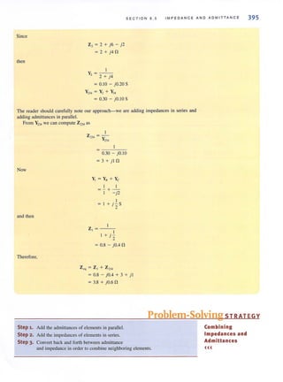
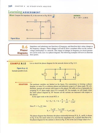
![SECTION 8.6 PHASOA DIAGRAMS 397
Ie Ie
IR
IR V V
IL + Ie
IL
IsIL
(a) (b)
Ie
Ie + IL
Is
IR V
IL
(c) (d)
that is, those for which Ie is greater than IL-the phasor diagram for the currents is shown
in Fig. 8.14c. Note that as w increases, the phasor Is moves from Is, to Is. along a locus of
points specified by the dashed line shown in Fig. 8.14d.
Note that Is is in phase with V when Ie = ILor, in other words, when wL = l /wC.
Hence. the node voltage V is in phase with the current source Is when
I
w=--
vTC
This can also be seen from the KCL equation
Let us determine the phasor diagram for the series circuit shown in Fig. 8.ISa.
KVL for this circuit is of the form
I
= IR + wLl / 90° + - / -90°
we
If we select I as a reference phasor so that I = I M!Sr, then if wLl" > 1M/WC, the phasor
diagram will be of the form shown in Fig. 8.ISb. Specifically, if w = 377 radls (i.e.,
f = 60 Hz), then wL = 6 and l /wC = 2. Under these conditions, the phasor diagram is as
shown in Fig. 8.ISc. If, however, we select Vs as reference with, for example,
Vs(') = 12 V2 cos(377' + 90°) V
~••• Figure 8.14
Phasor diagrams for the
circuit in Fig. 8.13.
[hint]
From a graphical standpoint.
phasors can be manipulated
like vectors.
EXAMPLE 8.13
•
SOLUTION
•](https://image.slidesharecdn.com/basicengineeringcircuitanalysis9thirwin-160630150938/85/Basic-engineering-circuit-analysis-9th-irwin-419-320.jpg?cb=1719934140)
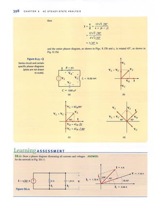
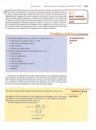
![SECTION B.8 ANALYSIS TECHNIQUES 401
Note that 12and 13could have been calculated by current division. For example, 12could
be determined by
1,(8-j4)
12 = 8 - j4 + j6
Finally, V2 can be computed as
(2.5 ~)(8.94 /-26.57')
8 + j2
= 2.71 /- 11.55' A
v, = 13(- j4)
= 7.28 / 15' V
This value could also have been computed by voltage division. The phasor diagram for the
currents 11 12 • and IJis shown in Fig. 8.l6b and is an illustration of KCL.
Finally, the reader is encouraged to work the problem in reverse; that is, given Vz. find
Vs. Note that if V, is known, 13can be computed immediately using the capacitor imped-
ance. Then V, + 13(S) yields V,. Knowing V, we can find I,. Then I, + 13 = I " and so on.
Note that this analysis, which is the subject of Learning Assessment ES.12, involves simply
a repeated application of Ohm's law, KCL, and KVL.
Learning ASSESSM E N T
E8.12 In the network in Fig. ES.12, Vo is known to be 8/ 45' V. Compute Vs· iii
2n 12 -j2n +
Vs 2n
Figure E8.12 ~------~--------.------40
In this section we revisit the circuit analysis methods that were successfully applied earlier
to dc circuits and illustrate their applicability to ac steady-state analysis. The vehicle we
employ to present these techniques is examples in which all the theorems, together with
nodal analysis and loop analysis. are used to obtain a solution.
Let us detennine the current 10in the network in Fig. 8. 173 using nodal analysis, loop analy-
sis, superposition, source exchange, Thevenin's theorem, and Norton's theorem.
1. Nodal Allalysis We begin with a nodal analysis of the network. The KCL equation
for the supernode that includes the voltage source is
~ -2 ~ + V' +~=O
l + j 1 1 - j
ANSWER:
Vs = 17.89 /-18.43' V.
8.8
Analysis
Techniques
EXAMPLE 8.15
•
SOLUTION
[hint]
Summing the current, leaving
the supernode. Outbound
currents have a positive sign.
•](https://image.slidesharecdn.com/basicengineeringcircuitanalysis9thirwin-160630150938/85/Basic-engineering-circuit-analysis-9th-irwin-423-320.jpg?cb=1719934140)
![402 CHAPTER 8 AC STEADY-STATE ANALYSIS
j1fl 1 fl j 1 fl
6&V
1 fl
-+
1 fl - j 1n 1 fl
10
~ - j 1fl
~
(a) (b)
..:,
: Figure 8.17 Circuits used in Example 8.15 for node and loop analysis.
[hint]
Just as in a de analysis. the
loop equationsassume that a
decrease in potential level
is + and an increase is - .
and the associated KVL constraint equation is
Solving for VI in the second equation and using this value in the first equation yields
v, - 6/!J:.. V,
- - 2 /!J:.. + V, + - -- ~ 0
I + j I - j
or
[
I I ] 6 + 2 + 2j
V, J+j + I +I"="j = I +j
Solving for Vz, we obtain
(
4 + .)
V, = I +~ V
Therefore,
1 = - -' = ~ - - j A4+' (- 3), I + j 2 2
2_Loop Allalysis The network in Fig. 8. 17b is used to perfonn a loop analysis. NOle
that one loop current is selected that passes through the independent current source.
The three loop equations are
1, =-2/!J:..
1(1, + I,) +j I(I,+I,) - 6/!J:.. + t(I, +I,) - j t(I, +I,) = 0
II, + 1(1, + I,) - jl(I, + I,) = 0
Combining the first two equations yields
1,(2) + 1,( 1 - j) = 8 + 2j
The third loop equation can be simplified to the form
1,( 1 - j) + 1,(2 - j ) = 0
Solving this last equation for 12and substituting the value in ~o the previous equation
yields
[
-4 + 2j ]
I, . + I - j = 8 + 2j
I - J
or
- 10 + 6j
I , = 4](https://image.slidesharecdn.com/basicengineeringcircuitanalysis9thirwin-160630150938/85/Basic-engineering-circuit-analysis-9th-irwin-424-320.jpg?cb=1719934140)
![SECTION 8 . 8 ANA LYSIS T E CHN I QUES 403
and finally
3. Superpositioll In using superposition, we apply one indepeodent source at a time.
The network in which the current source acts alone is shown inFig. 8. 18a. By combining
the two parnllel impedances on each end of the network, we obtain the circuit in
Fig. 8.18b, where
(I +j){ 1 -j)
Z' = In
(I + j) + (I - j)
Therefore, using current division
I~ = I ~A
The circuit in which the voltage source acts alone is shown in Fig. 8. 18e. The voltage
VI' obtained using voltage division is
and hence,
Then
(6~)[ 1(1 - j)]I + I -}
V;' = ----=.,.--:-:,,---';-=~
I + . + [ 1(1 - j) ]
} I + I - j
6( 1 - j)
= V
4
I, = ~ (I - j) A
6 (5 3)I. = I~ + I ; = I + 4" ( I - j ) = 2" - "2 j A
4. Source Exchallge As a first step in the source exchange approach, we exchange the
current SOurce and parallel impedance for a voltage source in series with the imped-
ance, as shown in Fig. 8. 19a.
, n
(a)
, n
I'o
, n
(e)
+
V;' 1 n
I"o
, n
I'o
(b)
"I'=-i' n
[hin tj
In applying superposition in
this case, each source is
applied independently and
the results are added to
obtain the solution.
~... Figure 8.18
Circuits used in Example 8.15
for a superposition analysis.](https://image.slidesharecdn.com/basicengineeringcircuitanalysis9thirwin-160630150938/85/Basic-engineering-circuit-analysis-9th-irwin-425-320.jpg?cb=1719934140)
![C HAPTER 8 AC STEADY-STATE ANALYS I S
Figure 8.19 ·"t
Circuits used in
Example 8.15 for a source
exchange analysis.
[
6 + 2(1 + i)]A
1 + J
[hin t]
t
In source exchange. a voltage
source in series with an
impedance can be exchanged
for a current source in
parallel with the impedance.
and vice versa. Repeated
application systematically
reduces the number of
circuit elements.
[hi n t]
In this Thevenin analysis.
1. Remove the 1-0 load and
nnd the voltage across the
open tl!rminals. Voc.'
2. Determine the impedance
Zmat the open terminals
with all sources made
zero.
3. Construct the following
circuit and determine I".
(a)
1 n 1 n
1 n
il n ~ r -il n
r
10
(b) (e)
Adding the two voltage sources and transfonning them and the series impedance
into a current source in paraliel with that impedance are shown in Fig. 8. 19b.
Combining the two impedances that are in paraliel with the I·n resistor produces
the network in Fig. 8. 19c, where
( I + j)( I - j)
Z = In
l + j+l-j
Therefore, using current division,
10 = CI:;)G)
= (%-~j)A
=4+j
I + j
5. Thevellin Alla/ysis In applying Thevenin's theorem to the circuit in Fig. 8.17a, we
first find the open-circuit voltage, Voc , as shown in Fig. 8.20a. To simplify the analysis,
we perform a source exchange on the left end of the network, which results in the
circuit in Fig. 8.20b. Now using voltage division,
Voc = [6+2( I +j) J[ I.-j .JI - )+I+}
or
Voc = (5 - 3j) V
The Thevenin equivalent impedance. Zllil obtained at the open-circuit terminals when
the current source is replaced with an open circuit and the voltage source is replaced
with a shon circuit is shown in Fig. 8.20c and calculated to be
(1+j)(I-j)
Z = = In
Th l +j + l - j](https://image.slidesharecdn.com/basicengineeringcircuitanalysis9thirwin-160630150938/85/Basic-engineering-circuit-analysis-9th-irwin-426-320.jpg?cb=1719934140)
![SECTION 8 .8 ANALYSIS TE C HN I QUE S 407
and the KCL equations for the nodes of the network are
v-v, v-v V
+ 3 - _ 4 '00 + 3 0 + ..2 = 0
I t..:::.... I jl
V, - V,
- j l
v,- V, (V,-V,)+ - 2 = 0
I I
V - V V
4 ~+ 0 3 +---E.= 0
I I
At this poin( we can solve the foregoing equations using a matrix analysisor, for exam-
ple, substitute the first and last equations into the remaining two equations, which
yields
3V, - ( I + n V, = - (4 + j12 )
-(4 + j 2)V, + ( I + n V, = 12 + jl6
Solving these equations for Voyields
V = _- o.:(8_+--"::-j4-,-)
, I + j2
= +4 / 143. 13" V
2 . Loop Analysis The mesh currents for the network are defined in Fig. 8.22c. The
constrai.nt equations for the circuit are
I, = -4 ~
I , = 14 - I, = 14 + 4 ~
I, = 21, = 21, + 8 ~
The KVL equations for mesh I and mesh 4 are
- j ll , + 1(1, - I,) = - 1 2~
j l(14 - I,) + 1(1, - I,) + II, = 0
Note that if the constraint equations are substituted into the second KVL equation, the
only unknown in the equation is I , . This substitution yields
I, = +4 / 143.13" A
and hence,
v, = +4 / 143.13" V
3. Thevellill 's Theorem In applying Thevenin's theorem, we will find the open-circuit volt-
age and then determine the Thevenin equivalent impedance using a test source at the open-
circuit terminals. We could determine the Thevenin equivalent impedance by calculating
the short-circuit current; however, we wi.1I detennine thiscurrent when we apply Nurtun's
theorem.
The open-circuit voltage isdetennined from the network in Fig. 8.23a. Note that
I ~{ = 41!!.... A and since 2I~ flows through the inductor, the open-circuit voltage Voc is
Voc = - 1 (4 ~) + j l(21:.)
=-4 + j8 V
To determine the Thevenin equivalent impedance, we turn off the independent sources,
apply a test voltage source to the output terminals, and compute the current leaving the
test source. As shown in Fig. 8.23b, since I; flows in the test source, KCL requires that
[hint]
How does the presence of a
dependent source affect
superposition and source
exchange?](https://image.slidesharecdn.com/basicengineeringcircuitanalysis9thirwin-160630150938/85/Basic-engineering-circuit-analysis-9th-irwin-429-320.jpg?cb=1719934140)
![S E CTION 8. 8 A NAL Y SI S TECHNI Q UE S
1 n
- (8 + j4)
. A
1 + } t
21'; ;; " -j l n
(a)
l' Figure 8.24 Circuits used in Example 8.16 when applying Norton's theorem.
Substituting the first and last equations into the remaining equations yields
(1 + j)V, - (3 + j)1;' = j l2
- (I + j)V, + (2)1;' = 4 - j l2
Solving these equations for I;' yields
-4
l "'=-- A
.t I + j
The KCL equation at the right-most node in the network in Fig. 8.24a is
1''' = 4 10° + 1, L::..- ~
Solving for Isc:, we obtain
- (8 + j4)
1 = A
51: I + j
The Thevenin equivalent impedance was found earlierto be
(b)
Using the Norton equivalent network, the original network is reduced to that shown in
Fig. 8.24b. The voltage Vois then
y = - (8 + j4) [ (1)(1 - j)]
o I +j I + I - j
=-4[~]3 + j
= +4 /+ 143.l3° Y
+
1 n Vo
10](https://image.slidesharecdn.com/basicengineeringcircuitanalysis9thirwin-160630150938/85/Basic-engineering-circuit-analysis-9th-irwin-431-320.jpg?cb=1719934140)
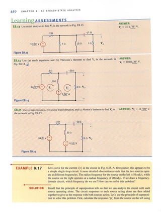
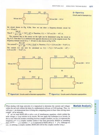
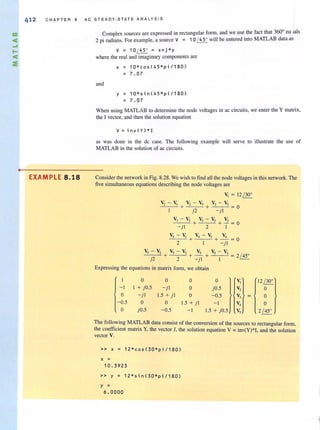
![SEC TIO N 6.6 ANA LYSIS TE CHN I Q UE S 413
12QQ.' V +
» v1 ;;: x+j*y
v1 =
10.3923 + 6.0000i
-j1n V
3
» 12 = 2*cos(45*pi/180) + j*2*sin ( 45*pi/180)
12 =
1.4142 + 1 . 4142i
1 n
» y = [1 0 0 0 0; -1 1+j*0.5 - j*1 0 j*0.5; 0 -j*1 1.5+j*1 0
-0.5; -0 . 5 0 0 1.5+j*1 -1; 0 j*0.5 -0.5 -1 1.5+j*0.5J
y =
Columns 1 through 4
1.0000 0
-1.0000 1.0000 +0.5000i
0 0 -1.0000i
-0.5000 0
0 0 +0.5000i
Column 5
o
o +0 . 5000i
-0 . 5000
-1 . 0000
1.5000 +0.5000i
» I ;;: Cv1; 0; 0; 0; 12]
1 =
10.3923 +6 . 0000i
o
o
o
1.4142 +1 . 4142i
0 0
0 -1.0000i 0
1 . 5000 +1.0000i 0
0 1.5000 +1.0000i
-0.5000 -1.0000
~... figure 8.28
Circuit used in Example 8.18.](https://image.slidesharecdn.com/basicengineeringcircuitanalysis9thirwin-160630150938/85/Basic-engineering-circuit-analysis-9th-irwin-435-320.jpg?cb=1719934140)
![•
414 C H A P T ER 8 A C S TE A DY · STATE A N A LYS I S
» V ;: i nv ( Y) *1
v =
1 0. 3923 +6 . 000 0 ;
7 . 0766 +2 . 1 580;
1 . 40 38 +2.5561;
3.766 1 - 2 . 962 1;
3.4 1 5 1 - 3 . 6771 ;
EXAMPLE 8.19 Consider the circuit shown in Fig. 8.29a. We wish to determine the current 10 , In contrast to
the previous example, this network contains two dependent sources, one of which is a cur-
rent source and the othera voltage source. We will work this problem using MATLAB here
and then address it again later using PSPICE.
•
SOLUTION Our method of attack will be a nodal analysis. There are six nodes, and therefore we will
need five linearly independent simultaneous equations to determine the nonreference node
voltages. Actually, seven equations are needed, but two of them simply define the depend-
ent variables. The network is redrawn in Fig. 8.29b where the node voltages are labeled. The
five required equations, together with the two constraint equations, needed to determine the
node Voltages. and thus the current Ill. are listed as follows:
~-V, v - v, - - 2 +' 4+ 21 =0
I _j .f
V, = 2V,
V, - V, = 12
V,- V, V3 V4 V - V V - V
2 + .+- + _+ 4 5 + 4 ]= 0
I 1 1 - j
V, - V, V,
+ - = 21I j .r
Vol = V3
V,
1= -, I
Combining these equations and expressing the results in matrix form yields
I +j -I 0 2-j 0 V, 2
0 1 - 2 0 0 V, 0
0 0 - I 0 V3 12
-j - I 2 2 + j - I V, -2
0 0 0 -3 I - j V, 0
The MATLAB solution is then
» y = [ 1 + j*1 - 1 0 2 - j*1 0 i 0 - 2 0 0; 0 0 - 1 1
- j*1 - 1 2 2+j*1 -1; 0 0 0 -3 1 -j*1 J
Y =
Column s 1 through 4
1.0000 +1.0000; - 1.0000 0 2 . 0 0 00
0 1 . 00 00 -2 . 0000 0
0 0 - 1.0000 1 . 0 0 00
0 -1.0000 ; -1.0000 2.0000 2 .00 0 0
0 0 0 - 3 . 0000
O·,
- 1 . 0000;
+1. 0000;](https://image.slidesharecdn.com/basicengineeringcircuitanalysis9thirwin-160630150938/85/Basic-engineering-circuit-analysis-9th-irwin-436-320.jpg?cb=1719934140)
![Column 5
o
o
o
- 1.0000
1 n
1 n
1 n
1 n
2V +
1.0000 - 1.0000;
t
10
1 n
1 n
2&A
-j1n
12&V
-+
+ I., 1 n
V, 1 n
(a)
1 n
1 n
(b)
» I = (2; 0; 12; -2; 0]
1 =
2
0
12
-2
0
» V = ;nv(Y) *1
V =
-5.5000 +4.5000;
-26.0000 -2 4. 0000;
-13.0000 -12.0000;
-1.0000 -12.0000;
16 .5000 -19.5000;
»
As indicated in Fig. 8.29b, 10is
10 = (V, - V,)/I
= - 13 - jl2 A
SEC TION 6.6 ANALYSIS TECHNIQUE S 415
f·· Figure 8.29
Circuit used in Example 8.19.
I 21x
j1n
j1 n](https://image.slidesharecdn.com/basicengineeringcircuitanalysis9thirwin-160630150938/85/Basic-engineering-circuit-analysis-9th-irwin-437-320.jpg?cb=1719934140)
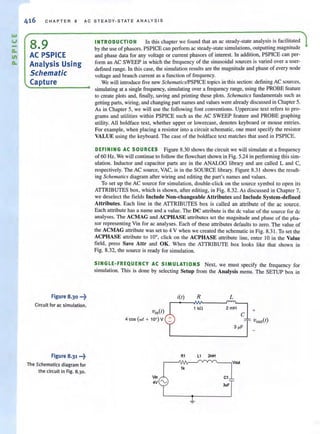
![SECTION 8.9 AC PSPICE ANALYSIS USING SCHEMATIC CAPTURE 417
Vin PartName: VAC (BJ
Name
loc
DC=OV
ACMAG.4V
ACPHASE·l0
Value
· IOV
r Include Non-changeobl. Attributes
r Include System·deflned Attributes
SaveAttr I
Change Oisploy I
Delete
OK
Cancel
Analysis Setup (8J
Enabled
IEnabled
~ ACSweep... Options...
II eme
r Load Bias Point...
I r Parametric,,,
I
r Save Bias Point.. I r Sensitivit)I...
I
r DC Sweep... I r T_atur•...
I
r Monte CariolWcwst Ces•...
I r TromIer FtI"lCtion...
I
~ Bias Point Delai I r Transient..
IDiglol Setup... I
AC Sweep and Noise Analysis (BJ
AC Sweep Type Sweep Parameter.
r. Line.r Teta! Pts.: 11
r Octave Start Freq.: IGO
r Decade End Freq.: IGO
Noise Analysis
r Noise Enabled
OutputVoltage: I
IN I
Interval: I
[]EJ Cancel I
Fig. 8.33 should appear. If we double-click on the text AC Sweep, the AC SWEEP AND
NOISE ANALYSIS window in Fig. 8.34 will open. All of the fields in Fig. 8.34 have been
set for aUf 60-Hz simulation.
Since the simulation will be performed at only one frequency, 60 Hz, graphing the simula-
tion results is not an attractive option. Instead, we will write the magnitude and phase of the
~••• Figure 8.32
Setting the ac source phase
angle.
~... Figure 8.33
The ANALYSIS SETUP window.
~... Figure 8.34
Setting the frequency
range for a single
frequency simulation.
."
11
."
-t"I
'"](https://image.slidesharecdn.com/basicengineeringcircuitanalysis9thirwin-160630150938/85/Basic-engineering-circuit-analysis-9th-irwin-439-320.jpg?cb=1719934140)
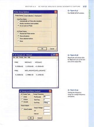
![42 0
-
CHAPTER 8 AC STEADY-STATE A NALYS IS
n.er. [,dt '!11M ~ 11- eIoI fQOlJ ~!:tIt> 11ft
~. "" ~ " 5 III ' ~. e ~--c]jI,""-"'E_=---- '~
t~ Ifi'h ..!! II=:,. '1/ '.. d !~7t; '" :f '" ;<! ,~ .. '" r.; ..t
~
~
'fI
..iI
IliI
111Hz
Main
Display
Window
1 ....1
f"fqut.c:~
... E_ _Ir---------------------------------~~----------------------------------~
Output
Window
rI'll Sim~lation Statu~ Win~ow
~ ~.......~7
..... _fl ,,"- lo.o:r.+06 UtO'Jlo mm....___,
oop
Figure 8,40 :
The PROBE window. VPRINTI and IPRINT parts in Fig. 8.35. Second, we return to the PROBE SETUP window
shown in Fig. 8.37, and select Automatically Run Probe After Simulation and OK.
CREATING PLOTS IN PROBE When the PSPICE simulation is finished, the PROBE
window shown in Fig. 8.40 will open. Actually, there are three windows here: the main display
window, the output window, and the simulation status window. The latter two can be toggled
off and on in the View menu. We will focus on the main display window, where the frequency
is displayed on a log axis, as requested. To plot the magnitude and phase ofVout , select Add
from the Trace menu. The ADD TRACES window shown in Fig. 8.41 will appear. To display
the magnitude of Vout, we select V(Vout) from the left column. When a voltage or current
is selected, the magnitude of the phasol' will be plotted. Now the PROBE window should look
like that shown in Fig. 8.42.
Before adding the phase to the plot, we note that Vout spans a small range-that is, 0 to 4 V.
Since the phase change could span a much greater range, we will plot the phase on a second
y-axis. From the Plot menu, select Add Y Axis, To add the phase to the plot, select Add from
the Trace menu. On the right side of the ADD TRACES window in Fig. 8.41, scroll down to
the entry, PO. Click on that, and then click on V(Vout) in the left column. The TRACE
EXPRESSION line at the bottom of the window will contain the expression P(V(Vout) )-the
phase of Vou!. Figure 8.43 shows the PROBE plot for both magnitude and phase of Vou!.
To plot the current, I, on a new plot, we select New from the Window menu. Then, we
add the traces for the magnitude and phase of the current through RI (PSPICE calls it I(Rl))
using the process described above for planing the magnitude and phase of Vout. The results
are shown in Fig. 8.44.
The procedures for saving and printing PROBE plots, as well as the techniques for plot
manipulation and data extraction, are described in Chapter 7.](https://image.slidesharecdn.com/basicengineeringcircuitanalysis9thirwin-160630150938/85/Basic-engineering-circuit-analysis-9th-irwin-442-320.jpg?cb=1719934140)
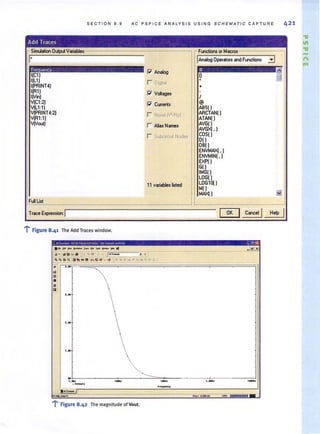
![..,
V
422 C H A PTER 6 AC STEADY·STATE ANALYSIS
_ " I"""r" ),{J.j, r~r~~ HI r....." l .. •• ....pto,...-"..II
r. '- rx
. !JiII OIl ..... . . - tr_ eot JIlIiI . - ~ II ..l4J.l!.
..filS 1.1. _ .!__~~ ..: ~'C(_ ."
~"QQ, iIItrM!! I::o ~ ¥ ...... d' ... Th.""'4 ~~er ..<,
- - - -----
• ..• , ,-
..if!
••!Ii nOQnil~
,.• ,-
... •
,.• .,- ~
~»
• -,- -
,.- n_ ,- '-- ,-,rn •'t_U III . '('1-1» ,~..~~-
~
-~
__ It.cm:;a.-='
ICIII'lIo--'".......... _
-r- Figure 8.43 The magnitude and phase ofYout.
:: l( I'''''r¥ (he,n I'pk. ,J{I [Ion.. I 'll) ~( r .....p.. ,,,,U... II C ~c rx:
• ..-, ,-
..if!
••III
..-
z._ ..
,.-
_1~' +'________+-________+-__________+-__C=~_____~
,.~ ,.-, ,.., 1._ ,_,•
[]} • Itl1) ttl • • (lCI"1))
,~.
-:..l Figure 8.44 The magnitude and phase of the (urrent, I.](https://image.slidesharecdn.com/basicengineeringcircuitanalysis9thirwin-160630150938/85/Basic-engineering-circuit-analysis-9th-irwin-444-320.jpg?cb=1719934140)
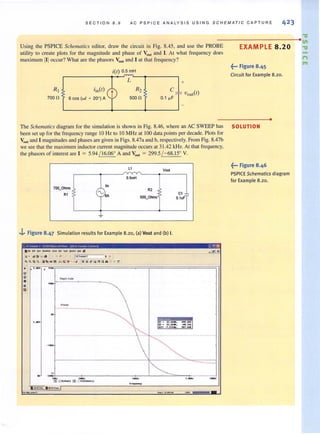
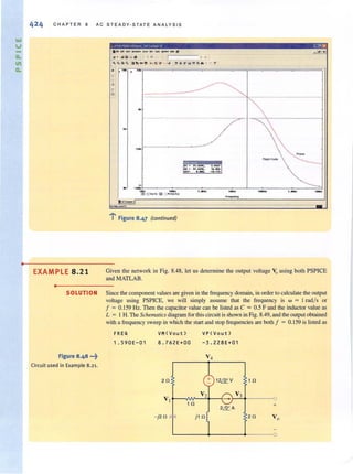
![SEC TION 8.9 AC PSPICE AN A LYSIS USING SCHEMATIC CAPTURE
"
"
12Y ......... V)
"
" V2
" ", ,?
" (
,.
""co
••• "
,
"
The nodal equations for the network are
v, - V, = 12
V4 -VI V4 -V3 V2 -VI "2
-'--::---'- + + + 2 + -= 0
2 I I jl
V1 - V4 V, VI - V,
---'--::---= + - + - = 0
2 -j2 I
V) -V4 ' j
-"----= + - = 2
I 2
These equations can be placed in the following format, and the MATLAB solution is then
listed as follows:
Ovl - v2 + Ov3 + v4 = 12
(- I + j3 )vl - j2v2 + Ov3 - jv4 = 0
- j3v l + (2 + j2)v2 - j2v3 + j 3v4 = - j4
Ovl + Ov2 + 3v3 - 2v4 = 4
» y ; [ 0 - 1 0 1; -1+(3*j l -2*j 0 -1 * j;
- 3 * j 2+2*j -2*j 3*j; 0 0 3 -2]
y ;
» ;
; ;
» v
v ;
0 -1
-1 + 3; 0 -
0 - 3; 2 +
0 0
; [12; O· -4*j;,
12
0
0 - 4;
4
; inv( y) *1
-1. 1192 - 6.6528;
-2.9 016 - 7.0259;
7.3990 - 4 . 6839;
9.0984 - 7 . 0259;
0
2; 0 0 -
2; 0 - 2; 0 +
3 -2
4]
1;
3;
~••• Figure 8.49
PSPICE Schematics diagram
for the network in Fig. 8.48.
"III
"n
fit](https://image.slidesharecdn.com/basicengineeringcircuitanalysis9thirwin-160630150938/85/Basic-engineering-circuit-analysis-9th-irwin-447-320.jpg?cb=1719934140)
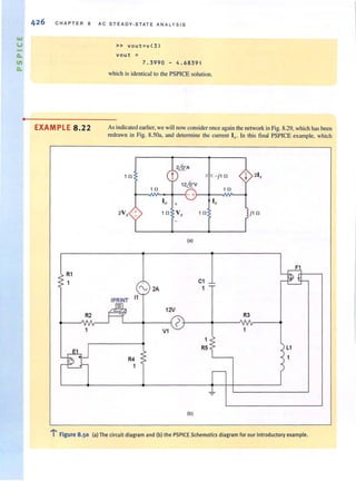
![SECTION 8 . 9 AC PSP I CE ANAL Y S I S USING SC HE MA T IC CA P TURE 42 7
contains two dependent sources--one current source and one voltage source-we will, once
again, outline in some detail the various issues that must be addressed in the solution.
Choosing the Frequency. In PSPICE we must specify inductors in henrys and capacitors in
farads even though reactive impedances are given in ohms in the frequency-domain schematic
in Fig. 8.50a. When the value of for w is not specified, we may choose any frequency we like,
and a very smart choice is w = I radl s (f = 1/ 27r = 0.1592 Hz). As a result, reactive im·
pedances are related to the inductor and capacitor values by simple expressions.
ZL = wL = L Zc = I / wC = I / C
To set the frequency, select SETUP from the ANALYSIS menu and choose AC SWEEP.
The window in Fig. 8.51 , already edited for this circuit, should open. By limiting the
frequency range to just one data point, making a plot of 10 versus frequency is silly. Instead,
we will obtain a printout for 10
•
Printing Currents and Voltages to the Output File. The IPRINT part, utilized
here, saves current values in the output file. The small negative sign marks the terminal
where current exits the part. To set up the !PRINT part, double-click on it to open the win-
dow in Fig. 8.52. We must indicate what kind of data we want to acquire. In this case, we
have used Y (short for "yes") to select the REAL and IMAGINARY components of the
AC Sweep and Noise Analysis [8]
r AC Sweep Type r Sweep Parameters
(;' Linear Totol Pt'.: 11
r Oct.ve Start Freq.: 10.1592
r Decode
End Freq.: 10.1592
~ Noise Anolysis
r Noise Enobled
Output Voltage: I
IN I
Intervol: I
[KJ Cancel !
PRINT1 PartName: IPRINT l8J
Nome
IDC
DC=
ACay
TRAN·
MAG·
PHASE-
REALay
IMAGay
Vu
·1
r Include Non-ehongeoble Atbilute.
r Include System-definedAlbibute.
Sov.Atb
Change Display !
Delele !
-' OK
~... Figure 8.51
Setting the frequency sweep to
a single frequency (0.1592 Hz)
such that wL = L.
~... Figure 8.52
Initializing the IPRINTpart
to print real and imaginary
current components from an
AC simulation.
"a
11
"a
n
rot](https://image.slidesharecdn.com/basicengineeringcircuitanalysis9thirwin-160630150938/85/Basic-engineering-circuit-analysis-9th-irwin-449-320.jpg?cb=1719934140)
![lAo!
V
a..
11
a..
CHAPTER 8 AC STEADY·STATE ANALYS I S
Figure 8.53 ...~
Setting the gain of the CCCS
to negative 2 offsets the
wiring differences between
Figs. 8.50a and b.
current that result from anAC simulation. When the simulation iscomplete, 10wiJI be at the
bottom of the output file. To log voltages to the output file, use the VPRlNTI and VPRINT2
parts. VPRlNTI measures node voltage with respect to the ground node, while VPRINT2
measures voltages between two nonreference nodes.
Current Direction in AC Current Sources. Dating back to the earliest forms of
SPICE, the current through current sources was defined as flowing into the terminal
marked with a + sign and out of the terminal marked with the - sign. Although this gives
the appearance that the source is consuming power, note that +/- markings are just that
and the voltage across the source will depend on the entire circuit. Look carefully at I I and
12 in Fig. 8.50b. They are connected exactly as shown in Fig. 8.50a.
Setting Dependent Source Gains. We will use the gain of the CCCS as an example.
Comparing Figs. 8.50a and b, it appears that the direction of Ix is reversed. This was done
to simplify the wiring between the CCCS and the branch where Ix is defined. By setting the
gain of the CCCS to lIegative 2, the circuits become identical. Now consider the VCVS,
which is wired in agreement with Fig. 8.50a. Here the gain is entered as positive 2. To set
the gain of a dependent source, simply double-click on it to open the attribute box shown in
Fig. 8.53 and enter the gain.
Accessing the OUTPUT FilE. When you simulate the circuit, the simulation engine in
PSPICE will open and the window in Fig. 8.54 will appear. When the simulation is com-
plete, close this window to return to Schematics where you can access the output file
through Examine Output File option in the ANALYSIS menu. When the OUTPUT FILE
opens, scroll to the bottom to find I•. You might notice that the output file window is actu-
ally the NOTEPAD text editor common to Windows-based PCs. So, you can copy and paste
the simulation results directly into other software.
When this circuit is simulated, the results in the output file are
FRE Q
1.592E-01
IR (V_PRINT1 J
-1.300E+01
II (V_PRINT1 J
-1.200E+01
which correspond to I. is -13-jI2 A, exactly the value calculated in Example 8.19. Note
that the current is listed as flowing through a part called V_P RI NT1. Again, dating back to
its origins, SPICE has always produced the node voltages and the currents through all volt-
age sources. So, an ammeter was easily "constructed" by inserting a voltage source set to
Ov. That is exactly what the !PRINT part is, a voltage source called V]RINT set to OV.
Fl PartName: F [EJ
Name Vu
IGAIN ·1·2
GAIN= 2
r Include Non-chang04ble Atbibutes
r Include System·definedAtbibutes
S.veAtt,
Change Display I
Delete
OK](https://image.slidesharecdn.com/basicengineeringcircuitanalysis9thirwin-160630150938/85/Basic-engineering-circuit-analysis-9th-irwin-450-320.jpg?cb=1719934140)

![•
430 CHAPTER 8 A C ST E ADY · STATE AN AL Y SI S
Figure 8.56 M·t
~
jwL
(aJModel used to reject
A
+ +
Vnois@ and (b) the required
Vinet) Vin
component. R Vo(t) R
Vo10 kn 10 kn
Vnoise(t) Vnoise
----0 ----0
(a) (b)
•
SOLUTION Consider the network in Fig. 8.56a. If component X has a high impedance, that is, much
greater than R at 700 k.Hz, and an impedance of zero at dc, we should be able to alleviate
the problem. Using voltage division to obtain Vo in Fig. 8.56b, we find
APPLICATION
EXAMPLE 8 .24
Figure 8·57 ···t
The general impedance
converter.
V - V[
R ]
,, - R + jwL I
where V, and w are either V;, and 0, or Voo;~ and 2"lT(700 X 103
) . At dc, w = 0, the inductor's
impedance is zero, the voltage division ratio is unity, VI is 'inand Vo equals "in. But at
700 kHz, VI is Vnoise and the desired voltage division ratio should be vel)' small; that is, the
inductor impedance must be much greater than R, so that Vo becomes nearly zero. If we
choose to reduce the noise at the output by 90%, we find
I R I= -'- at f = 700 kHz
R + jwL 10
Solving this equation yields L = 22.6 mH, which is close to a standard inductor value.
The circuit in Fig. 8.57 is called a General Impedance Converter. or Gle. We wish to devel-
op an expression for the impedance Zeq in terms of ZI' Z2. Z3. Z4' and Zs. and then using
resistors of equal value and a I-J.LF capacitor, create a J-H equivalent inductance.](https://image.slidesharecdn.com/basicengineeringcircuitanalysis9thirwin-160630150938/85/Basic-engineering-circuit-analysis-9th-irwin-452-320.jpg?cb=1719934140)
![(
SEC TI ON 8 . 11 DESIGN EXAMPL E S 431
•
We simply employ the ideal op-amp assumptions; that is, there is no current entering any SOLUTION
op-amp input, and the voltage across any op-amp's input terminals is zero. As a result, the
voltage at both nodes A and C are V;,. Next, we apply KCL at each op-amp input. At node A
V2- ~n =Vin
Z, Z,
which yields
v, = V[I+ Z,]- In ZI
At node C, we find
z, Z,
Solving for V, yields
V, = ,;,[1+ ~:] - v,[~:]
Substituting our resulls from Eq. 8.47, we can express VJ as
V, = V[1 _ Z,Z,]
. In Z IZ)
At node E, we write
Then using our expression for VJ in Eq. (8.48), we find that
[ Z,Z, ]lin = 'in Z Z Z
! 3 S
Finally, the impedance of interest is
VinZ =-
eq lin
Now, if Z, = Z, = Z, = Z, = R and Z, = l/ jwC, then Z'" becomes
Z cq = jwCR2
= jwLeq
8.47
8.48
8.49
Hence, the value of R necessary to yield a I-H inductance is 1000 n.At this point, we must
address the question: why go to all this trouble just to make inductance? The answer is size
and weight. A I-H inductor would be very large and heavy. The OIC is easy to construct with
integrated circuit components, requires very little space, and weighs only a few grams!
In Chapter 4 we found that the op-amp provided us with an easy and effective method of
producing controllable voltage gain. From these earlier studies, we have come to expect
gain from these "active" devices in a configuration like that shown in Fig. 8.58a. However,
•
8.11 JDesign Examples
DESIGN
EXAMPLE 8.25
•](https://image.slidesharecdn.com/basicengineeringcircuitanalysis9thirwin-160630150938/85/Basic-engineering-circuit-analysis-9th-irwin-453-320.jpg?cb=1719934140)
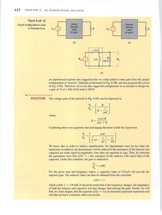
![SECTION 8.11 DESIGN EXAMPLES 433
A sinusoidal signal, v,(t) = 2.5 cos (wt ) when added 10 a dc level of V, = 2.5 V, provides a
0- to 5-V clock signal used to control a microprocessor. If the oscillation frequency of the
signal is to be I GHz, let us design the appropriate circuit.
As we found in Chapter 4, this application appears to be a natural application for an op-amp
summer. However, the frequency of oscillation (I GHz) is much higher than the maxi mum
frequency most op-amps can handle-typically less than 200 MHz. Since no amplification
is required in this case, we should be able to design an op-amp-less summer that, while not
precise, should get the job done.
Considerthe circuit in Fig. 8.59a where inputs v,(t) and V, are connected 10 yield the out-
put v.(t). For this application, component A should block any dc component in v,(t) from
reaching the output but permit the I-GHz signal to pass right through. Similarly, component
B should pass V, while blocking any high-frequency signal. Thus, the impedance of com-
ponent A should be infinite at dc but very low at I GHz. And the impedance of component
B should be zero at dc but very high at high frequency. Our earlier studies indicate that com-
ponent A must be a capacitor and component B an inductor. The resulting circuit, called a
bias T, is shown in Fig. 8.59b.
L
+ + ~+ +
VI(t) voCe) v,(e) voCe)
a a a a
(a) (b)
The values for C and L are dependent on both the signal frequency and the precision
required in the summing operation, and can be easily seen by using superposition to inves-
tigate the contribution of each input 10 v.(t). In Fig. 8.60a, the dc voltage V, has been
reduced to zero and an ac circuit has been drawn at a frequency of I GHz, that is, the fre-
quency of v,(t ). Using voltage division, we can express the output voltage as
v,,= [ jwL . ]v, = [ ,w2LC ]v,. L j w-LC - I
JW - we
8.50
Note that in order to achieve a perfect summer, the voltage division ratio must be unity.
However, such a voltage division ratio requires the impractical condition w2
LC equal infinity.
Instead, we wiU approach the problem by choosing values for the inductive and capacitive
reactances. As stated earlier, the capacitive reactance should be small; we choose I O. And the
inductive reactance should be large; let's say 10 kO. The resulting Land C values are
I
C = wXc = 21T X 10' 159 pF
and
L = XI. = 1.59 IJ.H
w
Now we consider 11,. In Fig. 8.60b, v,(t) has been reduced to zero and an ac circuit has
been drawn at dc- the frequency of 11,. Again, voltage division could be used to express the
DESIGN
EXAMPLE 8.26
•
SOLUTION
~... Figure 8.59
(a) A simple passive summer
circuit; (b) a solution-the
bias T.
•](https://image.slidesharecdn.com/basicengineeringcircuitanalysis9thirwin-160630150938/85/Basic-engineering-circuit-analysis-9th-irwin-455-320.jpg?cb=1719934140)
![•
434 CHAP TER 8 AC STEADY-STATE ANALYSIS
Figure 8.60 •••~
Exploring the bias·T
by steady·state
ac superposition
with (al v, ~ 0 and
(bl v,(t) ~ 0
-0
+
VI
j(O)L
---0
+
1/j(O)C V o2
o-------~-----__o
(a) (b)
output voltage. However, we see thai the impedances of the capacitor and inductor arc
infinity and unity, respectfully. As a result, the output is EXACTLY equal to V, regardless
of the values of C and L! Thus, the output voltage consists of two voltages. one at de and
the other at I GHz. The dc component is just V, = 2.5 V. From Eq. 8.50, the ac component
at I GHz is
Vo ' = [ JIO,OOO J2.5 /!!.. = 2.50025/!!.. V
JIO,OOO - jl
Back in the time domain, the output voltage is, to three significant digits.
V,( t) = 2.5 + 2.5 cos [2'lT( 109)t1V
SUMMARY
• The sinusoidal function definition The
sinusoidal function x(t) = XM sin (wt + 0) has an
ampl itude of X},f , a radian freq uency of w, a period of
2-rr/ w, "nd a ph"se "ngle of O.
• The phase lead and phase lag definitions If
x, (t) = X"" sin (wt + 0) and -,,(t) = X"" sin (wt + ~» ,
x,(t ) leads -,,(t) by 0 - 'I> radians and -,,(t) lags -,,(t) by
8 - ~ radians.
• The phasor definition The sinusoidal voltage
v(t) = VMcos(wt + 0) can be written in exponential form
as v(t ) = Re[V.u e"(wl +-O)] and in phasor form as V = V", f.!.
• The phase relationship in Ov and 0, for
elements R, 1., and C If Ouand OJrepresent the
phase angles of the voltage across and the current through a
circuit element, then 9j = 8u if the clement is a resistor, 0;
lags 8uby 90° if the clement is an inductor, 9, leads Ou
by 90° if the c lement is a capacitor.
• The impedances of R, 1., and C Impedance, Z,
is defined as the raLio of the phasor voltage, V, to the pha-
sor current, I, where Z = R for a resistor, Z = jwL for an
inductor. and Z = 1/ jwC fo r a capacitor.
• The phasor diagrams Phasor diagrams can be lIsed
to display the magnitude and phase relationships of various
voltages and currents in <I network.
• Frequency-domain analysis
1. Represent all voltages, viet) , and all currents, ij(t),
as phasors and represent all passive elements by their
impedance or adm ittance.
2. Solve for the unknown phasors in the frequency (w)
domain.
3. Transform the now-known phasors back to the time
domain.
• Solution techniques for ac steady-state
problems
Ohm's law
KCL and KVL
PSPICE
MATLAB
Nodal and loop analysis
Superposition and source exchange
Thevenin's theorem
Norton's theorem](https://image.slidesharecdn.com/basicengineeringcircuitanalysis9thirwin-160630150938/85/Basic-engineering-circuit-analysis-9th-irwin-456-320.jpg?cb=1719934140)
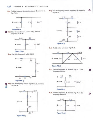
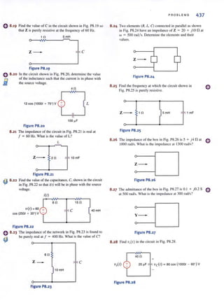
![438 C H AP TE R 8 AC STE ADY-S T ATE ANA LY SIS
8.29 Draw the frequency-domain network and calculate j(/)
in the circuit shown in Fig. PS.29 ifvl,(t) is 15 sin
(IOOOOt) V. Also. using a phasor diagram. show that
vcCt) + vR(t ) = v,(t).
itt) vc(t)
+ -
66.67 uF +
vAt)
Figure P8.29
8 .30 Draw the frequency-domain network and calculate
V,,(f) in the circuit shown in Fig. P8.30 if isCI) is
I cos(2500t - 45°) A. Also, using a phasor diagram,
show that icCt ) + iR(t) = i,(t ).
i,(t) 10 0
Figure P8.30
8 .31 Find id t) and i(t) in the network in Fig. P8.3 1.
vet) ~ 120 +
cas(5000t) V
Figure P8.31
itt)
600
16mH
8.32 Dmw the frequency-domain network and calculate eVII( t) in the circuit shown in Fig. P8.32 if fl{/) is200 cos
(lO't + 60") mA. i,(t ) is lOa sin ( IO't + 90") mA. and
vs(t) = 10 sin( IO't) V. Also. use a phasor diagram to
delcrrninc ve(r ).
+
Figure P8.32
8.33 If v,(t) = 20 cos 5t volts. find v.(t ) in the network in 0
Fig. P8.33.
30 0.5 H
r-~~~~~--~----~'---O
+
v,.(t) 1 H 10 0 0.02 F
L---------~____~____~.---O
Figure P8.33
8 .34 Find 'Vo(r ) in the circuit in Fig. P8.34.
20 0 200 ~F 30 mH 100 ~ F
+
10 []
170 cos 3771 V
20mH
Figure P8.34
8.35 Find Vet ) in the network in Fig. P8.35.
20 0.2 H
+
24 cos 201 V 0.02 F vet)
Figure P8.35
fl 8.36 Find vAl ) illlhe circuit in Fig. PS.36.
- 10 0 0.1 H 0.005 F
+
100 COS 40f V
50 0.2 H
Figure P8.36
t 2 cos (20t + 15") A
40 cos (401 - 30°) V](https://image.slidesharecdn.com/basicengineeringcircuitanalysis9thirwin-160630150938/85/Basic-engineering-circuit-analysis-9th-irwin-460-320.jpg?cb=1719934140)
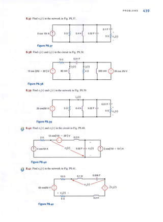
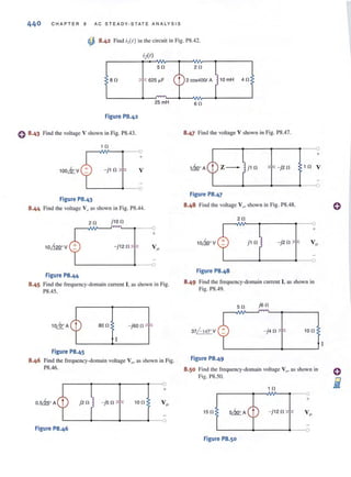
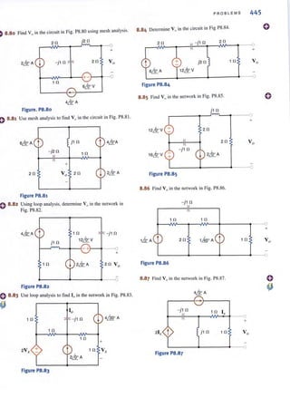
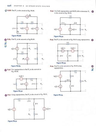
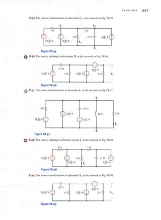
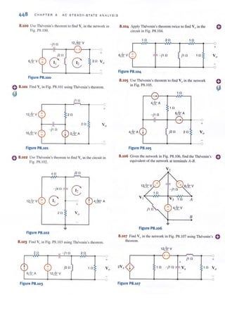
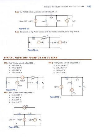
![454 CHAPTER B AC STEADY-STATE ANALYSIS
8FE-4 Determine the midband (where the coupli ng capacitors can be ignored) gain of
the single-stage transistor ampliJier showll in Fig. 8PFE-4.
a. 110.25
b. - 133.33
c. 26.67
d. - 95.75
~------~--~I~~ _____o
+
1 kO +
5 kn V,. 6 kO 12 kn Vo
L-----~__--~------~----~ _____o
Figure 8PFE-4
8FE-5 What is the currcnllo in the circuit in Fig. 8PFE-5?
a. 6.32L 30.31° A
b. 2.75L 21.43° A
c. 1.48L 32.92' A
d. 5.23L 40. 15' A
Figure 8PFE-S
30
j3 n )
1n
II
1
- ]1 n
1 0
10](https://image.slidesharecdn.com/basicengineeringcircuitanalysis9thirwin-160630150938/85/Basic-engineering-circuit-analysis-9th-irwin-476-320.jpg?cb=1719934140)

![•
456 CHAPTER 9 STEA D Y-S T AT E POW ER ANALYS IS
9.1
Instantaneous
Power
i(t)
v(t)
-=--,Figure 9.1
Simple ac network.
EXAMPLE 9.1
•
By employing the sign convention adopted in the earl ier chapters, we can compUle the in sla n ~
taneous power supplied or absorbed by any device as the product of the instantaneous volt-
age across the device and the instantaneous current through it.
Consider the circuit shown in Fig. 9. J. In genera l. the steady-state voltage and current fo r
the network can be wrincil as
The instantaneous power is then
V(I) = V:uCOS(WI + a,)
i(l) = I", COS (WI + a,)
p(l } = v(l}i(l }
Employing the followi ng trigonometric idcllIity,
I
cos <1>, cos ,~, = 2[cos(<I>, - <1>,) + cos(<I>, + <1>,)]
we find Ihal the instantaneous power can be written as
p(l } = V'~" [cos(a" - ail + cos(2wl + e, + ail]
9.1
9.2
9.3
9.4
9.S
Note that the instantaneous power consists of two tcrms. The first term is a constant (i.e., it
is ti me independent), and the second term is a cosine wave of twice the excitation frequency.
We wi ll examine this equation in more detail in Section 9.2.
The circuit in Fig. 9. 1 has the following parameters: V( I } = 4 cos (WI + 60°) V and
Z = 2 /300
n. We wish to detennine equalions for the current and the instantaneous power
as a function of time and plot these functions wilh the voltage on a single graph for
comparison.
SOLUTION Since
[hint]
Note that p(t) contains a dc
term and a cosine wave with
twice the frequency of v(t)
and i(I).
then
From Eq. (9.5),
4 / 60°
= 2 / 30°
= 2 / 30° A
i(l) = 2cos (wl + 30°) A
1'(1) = 4[cos(300) + cos(2wl + 90' )]
= 3.46 + 4 cos(2wl + 90°) W
A plOl of this function, together with plots of the voltage and current, is shown in Fig. 9.2.
As can be seen in this figure, the instantaneous power has a dc or constant term and a sec-
ond term whose frequency is twice that of the voltage or current.](https://image.slidesharecdn.com/basicengineeringcircuitanalysis9thirwin-160630150938/85/Basic-engineering-circuit-analysis-9th-irwin-478-320.jpg?cb=1719934140)
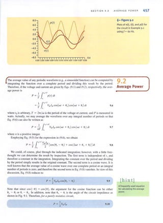
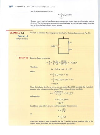
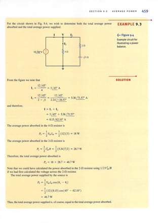
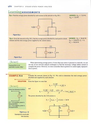
![SECTION 9.2
According to the direction of 13, the 61!r.-V source is absorbing power. The power it
absorbs is given by
I
P'12: = :2VAtIAt cos(6, - 6,)
= i(6)(7.44) cos[0° - (-36.21 °) ]
= 18W
At this point an obvious question arises: How do we know whether the 6 /!!....-V source is
supplying power to the remainder of the network or absorbing it?The answer to this question
is actually straightforward. If we employ our passive sign convention that was adopted in the
earlier chapters-that is, if the current reference direction enters the positive tenninal of
the source and the answer is positive-the source is absorbing power. If the answer is negative,
the source is supplying power to the remainder of the circuit. A generator sign convention could
have been used, and under this condition the interpretation of the sign of the answer would be
reversed. Note that once the sign convention is adopted and used, the sign for average pcwer
will be negative only if the angle difference is greater than 90° (i.e., 16, - 6,1 > 90°).
To obtain the power supplied to the network, we compute I I as
II = I , + I ,
= 6 / 30° + 7.44 /-36.21 °
= 11.29 / -7.10° A
Therefore, the pcwer supplied by the 12 / 300
-V source using the generator sign convention is
Ps = i(12)( 1I .29) cos (30° + 7.IO")
= 54 W
and hence the power absorbed is equal to the power supplied.
LearningAssEsSMENTS
E9.3 Detennine the total average power absorbed and supplied by each element in the network
in Fig. E9.3.
4n 4/300
V
Figure E9.3
E9.4 Given the network in Fig. E9.4, detennine the total average power absorbed or supplied
by eachelement.
2n
4n
Figure E9.4
AVERAGE POWER
ANSWER:
Pcs = -69.4 W;
Pvs = 19.8 W;
P,o = 49.6 W; Pc = O.
ANSWER,
P"12: = - 55.4 W;
PI212: = 5.5 W:
P,o = 22.2 W;
P,o = 27.7 W; PL = O.](https://image.slidesharecdn.com/basicengineeringcircuitanalysis9thirwin-160630150938/85/Basic-engineering-circuit-analysis-9th-irwin-483-320.jpg?cb=1719934140)
![CHAPTER 9 STEADY-STATE POWER ANALYS IS
9.3
Maximum
Average Power
Transfer
1'"" ---- ----- - - - ,,
,
:Voc
ac circuit
,
, -
---- ----------
F· 6 ..,...gure 9. i
Circuit used to examine
maximum average power
transfer.
[hint]
This impedance-matching
concept is an important
issue in the design of high·
speed computer chips and
motherboards. For today's
high·speed chips with
internal clocks running
at about 3 GHz and
motherboards with a bus
speed above 1 GHz,
impedance matching is nec-
essary in order to obtain the
required speed for signal
propagation. Although this
high·speed transmission line
is based on a distributed
circuit (discussed later in
electrical engineering
courses), the impedance-
matching technique for the
transmission line is the
same as that of the lumped
parameter circuit for
maximum average power
transfer.
In our study of resistive networks, we addressed the problem of maximum power transfer to a
resistive load. We showed that if the network excluding the load was represented by a
Thevenin equivalent circuit, maximum power transfer would result if the value of the load
resistor was equal to the Thevenin equivalent resistance (i.e., RL = RnJ We will now reex-
amine this issue within the present context {Q determine the load impedance for the network
shown in Fig. 9.6 that will result in maximum average power being absorbed by the load
impedance ZL'
The equation for average power at the load is
The phasor current and voltage at the load are given by the expressions
Voc
1/. = ::---"'--::-
ZTh + Z/.
where
and
The magnitude of the phasor current and voltage are given by the expressions
Voc
If. = .,-;-------,,-----'";-----C;-;-:-::-
[( )' ( )'l'/'R Th + RI. + XTh + Xl, -
9.11
9.12
9.13
9.14
9.15
9.16
9.17
The phase angles for the phasor current and voltage are contained in the quantity (SUI. - 8i J
Note also that SUI. - eiL
= 8ZL
and, in addition,
9.18
Subs.ituting Egs. (9.16) '0 (9.1 8) in.o Eg. (9. 11 ) yields
I V~ RL
PL
=,( )' ( )'- Rll1 + RL + XTh + Xt -
9.19
which could, of course, be obtained directly from Eq. (9.16) using PI- = 1 / 1RL' Once again,
a little forethought will save us some work. From the standpoint of maximizing Pl. , Voc is a
constant. The quantity (XTh + XL) absorbs no power, and therefore any nonzero value of this
quantity only serves to reduce PI.' Hence, we can eliminate this term by selecting
XL = - X Th · Our problem then reduces to maximizing
9.20
However, this is the same quantity we maximized in the purely resistive case by selecting
RI. = RTh · Therefore, for maximum average power transfer to the load shown in Fig. 9.6, ZL
should be chosen so .ha.
9.21](https://image.slidesharecdn.com/basicengineeringcircuitanalysis9thirwin-160630150938/85/Basic-engineering-circuit-analysis-9th-irwin-484-320.jpg?cb=1719934140)
![SECT I ON 9 .3 M AX IM UM AVERAGE POWER TRANSFER
Finally, if the load impedance is purely resistive (i.e., XL = 0). the condition for maxi-
mum average power transfer can be derived via the expression
where PI. is the expression in Eq. (9.1 9) with XL = O. The value of RJ. rhm maximizes PL
under rhe cO/u/irion XL = 0 is
9.22
Problem-Solving STRATEGY
Step 1. Remove the load ZL and find the Thevenin equivalent for the remainder of the
circuit.
Step 2. Construct the circuit shown in Fig. 9.6.
Step 3. Select Z,. = Zib = R'/"h - jXTh • and then I L = V.~/2 RThand the maximum
I . ., 2
average power transfer = '2IiR['h = Voc/ 8 R.fh ·
Given the circuit in Fig. 9.7a, we wish to find the value of Z L for maximum average power
transfer. In addition, we wish to find the value of the maximum average power delivered to
the load.
To solve the problem. we form a Thevenin equivalent at the load. Tbe circuit in Fig. 9.7b is
used to compute the open-circuit voltage
4!!!.. (2)
V = (4) = 5.26 /- 9.46' V
oc 6 + jl
The Thevenin equivalent impedance can be derived from the circuit in Fig. 9.7c. As shown
in the figure,
4(? + J'I )
Z = - = 1.41 + '0.43nTh 6 + jl J
Therefore, ZL for maximum average power transfer is
ZL = 1.41 - j0.43 n
With ZL as given previously, the current in the load is
5.26 /-9.46'
I = = 1.87 /- 9.46' A
2.82
Therefore, the maximum average power transferred to the load is
Maximum Average
Power Transfer
<((
EXAMPLE 9.5
•
SOLUTION
[hint]
In this Thevenin analysis.
1. Remove ZL and find the
voltage across the open
terminals, Voc '
2. Determine the impedance
ZTh at the open terminals
with aU independent
sources made zero.
) . Construct the foUowing cir-
cuit and determine I and
Pl'
•](https://image.slidesharecdn.com/basicengineeringcircuitanalysis9thirwin-160630150938/85/Basic-engineering-circuit-analysis-9th-irwin-485-320.jpg?cb=1719934140)
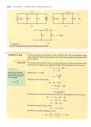
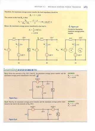
![•
CHAPTER 9 STEADY-STATE PO WE R A NALY SIS
9.4
Effective or
rms Values
EXAMPLE 9.7
In the preceding sections of this chapter, we have shown that the average power absorbed by
a resistive load is directly dependent on the type, or types, of sources that are delivering power
to the load. For example, if the source was dc, the average power absorbed was /2R, and if
the source was sinusoidal, the average power was 1/ 2/I, R. Although these two lypes of
waveforms are extremely important, they are by no means the only waveforms we will
encounter in circuit analysis. Therefore, a technique by which we can compare the effective-
lIess of different sources in delivering power to a resistive load would be quile useful.
To accomplish this comparison, we define what is called the effective value ofa periodic
waveform, representing either voltage or current. Although either quantity could be used. we
will employ current in the definition. Hence, we define the effective value of a periodic cur-
rent as a constant or dc value, which as current would deliver the same average power to a
resistor R. Let us call the constant current l eff. Then the average power delivered to a resistor
as a result of this current is
p = l ~ff R
Similarly, the average power delivered to a resistor by a periodic current i(t ) is
I / ,,,+'1'P = - ;'(I)R dl
T '"
Equating these two expressions, we lind that
I /" +T"" = T ;'(1) dl
."
9.23
Note that this effecti ve value is found by tirst determining the square of the current, then
computing the average or mean value, and finall y taking the square ro01. Thus, in "reading"
the mathemat.ical Eq. (9.23), we are determining the root mean square, which we abbreviate
as fill S, and therefore I cff is called Inns .
Since dc is a constant, the rms value of de is simply the constant value. Let us now deter-
mine the rms value of other waveforms. The most important waveform is the sinusoid, and
therefore, we address this particular one in the following example.
We wish to compute the nTIS value of the wavefonTI ;(1) = 1Mcos (WI - 6), which has a
period of T = 2",/w.
••----------------~
SOLUTION Substituting these expressions into Eg. (9.23) yields
Using the trigonometric identity
[
I 1T
, ,- 1- COS-(WI
T O M
- 6) dl
, I I
cos-<jJ = - + - cos 2<1>
2 2
we find that the preceding equation can be expressed as
]
1/'
I"", = IA/{?W ('n/w[_21 + +COS(2wl
_7T )0 _ ] }
I/'
- 26) dl
Since we know that the average or mean value of a cosine wave is zero,
(
W ('n/wI )1/'
Inns = 1'1 2'1T)0 "2 dt
IM[~ ('--) I" /W]1/2
27i 2 0
9.24](https://image.slidesharecdn.com/basicengineeringcircuitanalysis9thirwin-160630150938/85/Basic-engineering-circuit-analysis-9th-irwin-488-320.jpg?cb=1719934140)
![SECTION 9.4 EFFECTIVE OR RMS VA LUE S
Therefore, the rms value of a sinusoid is equal to the maximum value divided by the V2.
Hence, a sinusoidal current with a maximum value of 1M delivers the same average power
to a resistor Ras a de current with a value of 1",/V2. Recall that earlier a phasor X was
defined as X", ~ for a sinusoidal wave of the form X", cos (WI + e). This phasor can also
be represented as X",/V2~ if the units are given in rms. For example, 120 / 30' V rms is
equivalent to 170 / 30' V.
On using the rms values for voltage and current, the average power can be written, in
general, as
The power absorbed by a resistor R is
v'p = / 2 R = ~
nils R
9.25
9.26
In dealing with voltagesand currents in numerous electrical applications, it isimportant to
know whether the values quoted are maximum, average, nns, or what. We are familiar with
the 120-V <lC electrical outlets in our home. In thiscase, the 120 V isthe rms value of the volt-
age in our home. The maximum or peak value of this voltage is 12012 = 170 V. The voltage
at our electrical outletscould be written as 170 cos 3771 V. The maximum or peak value must
be given if we write the voltage in this form. There should be no question in our minds that
this is the peak value. It is common practice to specify the voltage rating of ac electrical
devices in terms of the rms voltage. For example, if you examine an incandescent light bulb,
you will see a voltage rating of 120 V, which is the rms value. For now we will add an nns to
our voltages and currents to indicate Ihar we are lIsing rms values in our calculations.
We wish to compute the rms value of the voltage waveform shown in Fig. 9.9. EXAMPLE 9.8
•
The waveform is periodic with period T = 3 s. The equation for the voltage in the time SOLUTION
frame 0 SIS 3 s is
{
41V
V(I) = OV
- 41 + SV
The nns value is
O < I $ l s
1 < 1 $ 2s
2 <1$3s
{
I [1' l' {3 ]}1/'v='=:3 0 (41)' dl + I (O)' dl + j , (S- 41 )'dl
= [k('~,JI: + ( 641 _ 6~I' + 1~(3) 1:)r
= I.S9 V
V(I) (v)
4
-4 ---- ---- ---
~••• Figure 9.9
Waveform used to
illustrate rms values.
•](https://image.slidesharecdn.com/basicengineeringcircuitanalysis9thirwin-160630150938/85/Basic-engineering-circuit-analysis-9th-irwin-489-320.jpg?cb=1719934140)
![•
468 CHAPTER 9 STEADY·STATE P OW ER ANALYS I S
EXAMPLE 9.9
•
Determine the rms value of the current waveform in Fig. 9.10 and use this value to compute
the average power delivered to a 2-0 resistor through which this currenl is flowing.
SOLUTION The current waveform is periodic with a period of T ; 4 s. The rrns value is
Figure 9.10 .~?
Waveform used to
illustrate rms values.
{I[J.' 1,' ]}'/2I~, ;;( o (4)' dt+ ,{-4)' dt
[ I ( I' 1')]'/2; ;( 16t 0 + 16t ,
;4A
The average power delivered to a 2-11 resistor with this current is
p ; I~" R ; (4)'(2) ; 32 W
Current (A)
itt)
4
2 0
-4
2 4 6 tIs)
Learning ASS ESSM EN T 5
E9.7 Compute the rms value of the voltage waveform shown in Fig. E9.7. ANSWER:
V ~, ; 1.633 V.
Figure E9.7
"''''',~---/1
o 2 4 6
/8 tIs)
E9.8 The current waveform in Fig. E9.8 is flowing through a 4-11 resistor. Compute the ANSWER: p ; 32 W.
average power delivered to the resistor.
itt) (A)
4
2 f--I
Figure E9.8 o 2 4 6 8 10 12 tIs)](https://image.slidesharecdn.com/basicengineeringcircuitanalysis9thirwin-160630150938/85/Basic-engineering-circuit-analysis-9th-irwin-490-320.jpg?cb=1719934140)
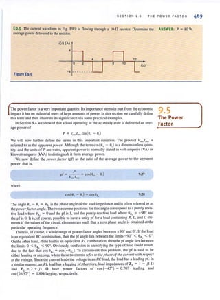
![•
470 CHAPTER 9 STEADY · STATE POWER ANALYSIS
EXAMPLE 9.10
•
SOLUTION
[hint]
Technique
1. Given Pi' pf, and Vrms•
determine'rms'
2 . Then Ps = PL+ 1;'5 Rline•
where RUneis the line
resistance.
Figure 9.11 •••~
Example circuit for
examining changes in
power factor.
An industrial load consumes 88 kW at a pf of 0.707 lagging from a 480-V rms line. The
transmission line resistance from the power company's transformer to the plant is 0.08 n.
Let us detennine the power that must be supplied by the power company (a) under present
conditions and (b) if the pf is somehow changed to 0.90 lagging. (It is economically advan-
tageous to have a power factor as close to one as possible.)
a. The equivalent circuit for these conditions is shown in Fig. 9.1 1. Using Eq. (9.27), we
obtain the magnitude of the rms current into the plant:
PL
Inns = -(-)-i("----:-)
pf Vm"
(88)(103
)
= c-:-==~::-::-:-
(0.707)(480)
= 259.3 Arms
The power that must be supplied by the power company is
Ps = PL + (0.08) / ;"',
= 88,000 + (0.08)(259.3)'
= 93.38 kW
b. Suppose now that the pf is somehow changed to 0.90 lagging but the voltage remains
constant at 480 V. The rms load current for this condition is
PL
1m" = -(p-f)"""(C~~-,)
(88)(103
)
(0.90)(480)
= 203.7 Arms
Under these conditions the power company must generate
Ps = PL + (0.08) /~m
= 88,000 + (0.08)(203.7)'
= 91.32 kW
Note carefully the difference between the two cases. A simple change in the pf of the
load from 0.707 lagging to 0.90 lagging has had an interesting effect. Note that in the first
case the power company must generate 93.38 kW in order (0 supply the plant with 88 kW
of power because the low power factor means that the line losses will be high-5.38 kW,
However, in the second case the power company need only generate 91.32 kW in order to
supply the plant with its required power, and the corresponding line losses are only 3.32 kW.
0.080
/480 V rms
""](https://image.slidesharecdn.com/basicengineeringcircuitanalysis9thirwin-160630150938/85/Basic-engineering-circuit-analysis-9th-irwin-492-320.jpg?cb=1719934140)
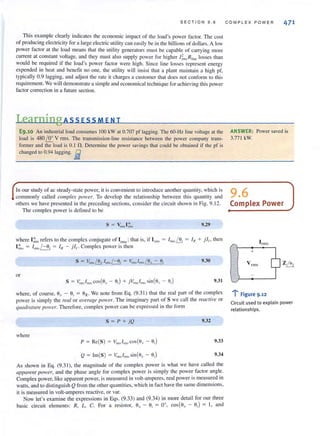
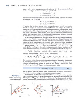
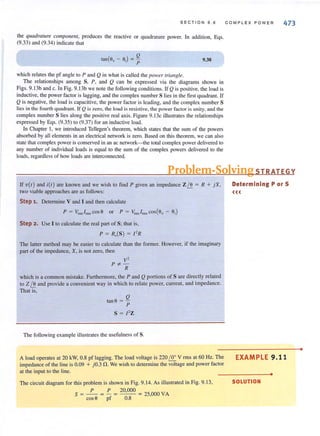
![474 CHAPTER 9 S TE ADY·STATE POWER A NA LY S I S
[hin tj
1. Use the given Pt. cos O.
and VL rms to obtain
SLand 1£based on Eqs.
(9·33) and (9.29),
respectively.
2. Use It and Zline to obtain
SUneusing Eq. (9·35)·
3· Use Ss = Stine + SL'
.€f. Vs = 55/ 1; yields Vs and
01/' Since Vs = Vs ~ and
0, is the phase of 1£'
pf = COS{O, - 0,).
figure 9,14 •.•~
Example circuit for
power analysis.
Therefore, al the load
SL = 25,000 ~ = 25,000 / 36.87° = 20,000 + j 15,000 VA
[25,000 ~ ] '
220I!r.
113.64 / -36.87° Arms
The complex power losses in the line are
= ( 113.64)'(0.09 + jO.3 )
= 1162.26 + j3874.21 VA
As stated earlier, complex power is conserved, and, therefore, the complex power at the
generator is
Ss = S/. + S lint
= 21 ,162.26 + jI8,874.21
= 28,356.25 / 41.73° VA
Hence, the generator voltage is
Vs = _Is_51 = _28.:...,3_56.,.....2_5
IL 113.64
= 249.53 V rms
and the generator power factor is
cos(41.73°) = 0.75 lagging
We could have solved this problem using KVL. For example, we calculated the load
current as
IL = 113.64 /-36.87° Arms
Hence, the voltage drop in the transmission line is
;"' = (113.64 /-36.87°)(0.09 + jO.3)
= 35.59 / 36.43° V rms
Therefore, the generator voltage is
Vs = 220 I!r. + 35.59 / 36.43°
= 249.53 / 4.86° V rms
Hence, the generator voltage is 249.53 V rms. In addition,
9, - 9; = 4.86° - (- 36.87°) = 41.73°
and Iherefore,
pf = cos{41.73°) = 0.75 lagging
0.09 n jO.3 n](https://image.slidesharecdn.com/basicengineeringcircuitanalysis9thirwin-160630150938/85/Basic-engineering-circuit-analysis-9th-irwin-496-320.jpg?cb=1719934140)
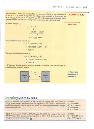
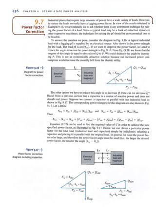
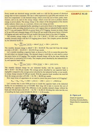
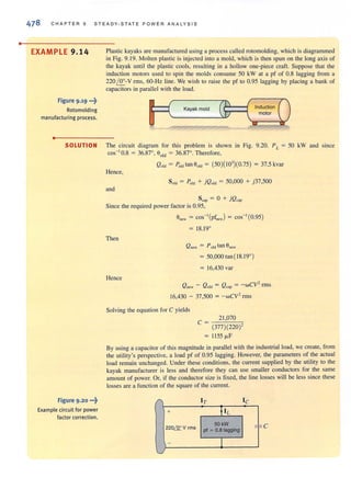
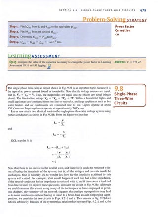
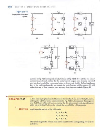
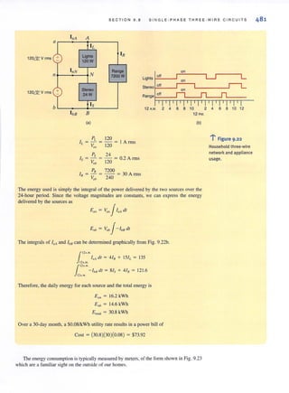

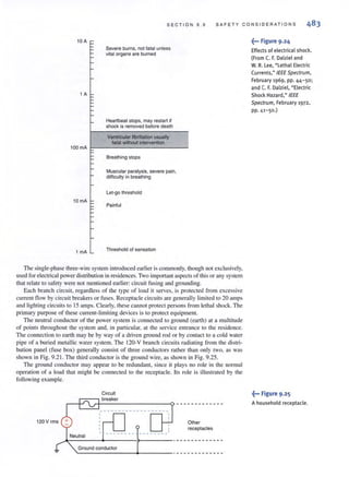
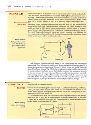
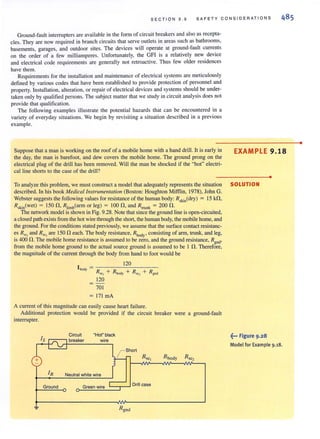
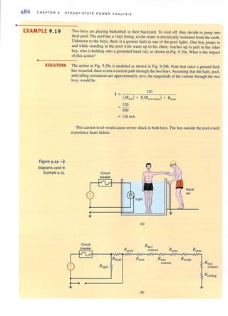
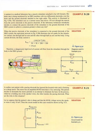
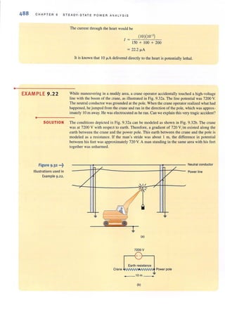

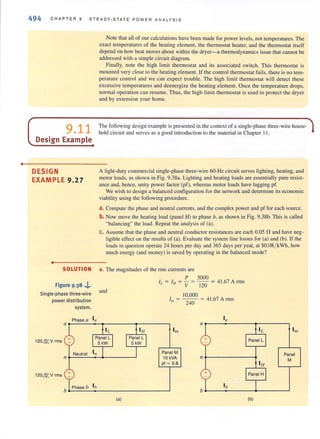
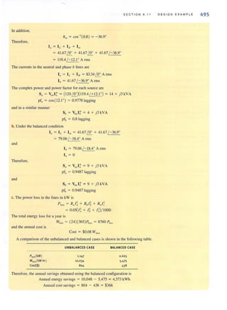
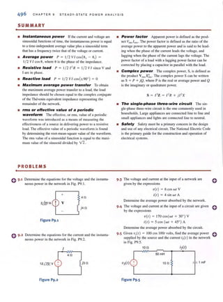
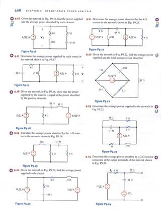
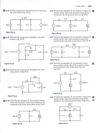
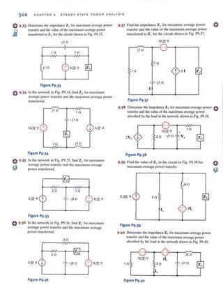
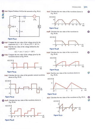
![502 CHAPTER 9 STEAD Y -ST ATE P OW ER A N ALYS IS
o 9 .52 C,alcu larc the rillS value of the waveform shown in
Fig. P9.52.
V(I) (v)
4
o
Figure P9.52
2 3 4 5 6 ((s)
e 9·53 The current waveform in Fig. P9.53 is llowing through a
5-n rcsislOr. Find [he average power absorbed by the
resistor.fl
- i(l) (A)
4
- 2
- 4
Figure P9.53
I(s)
9·54 Compute the fill S v<llue of the waveform in Fig. P9.54.
'0(1) (v)
4
o 10 I(s)
- 4
Figure P9.54
e 9·55 Calculate the nns value of the waveform shown in
Fig. P9.55.
i(l) (A)
o
I(S)
- 2
Figure P9.55
o 9·56 An industrial load consumes 100 kW ut 0.8 pI' lagging.
If an ammeter in the transmission line indie,ltes thar the
load curren( is 200 A rms, find the load voltage.
o 9·57 A plant consumes 20 kW of power from a 240- V fms
line. If the load power factor is 0.9. what is the angle by
which the load voltage leads the load current ? What is
the load current phasar if the line voltage has a phasor of
240 ~ Y rms?
e 9.58 A plant consumes 100 kW of power at 0.9 pf lagging. If
the load current is 200 A rms. find the load voliage.
9·59 An industrial plant with an inductive load consumes
10 kW of power from a 220-V nns line. If the load
power factor is 0.8, what is the angle by which the
load voltage leads the load current?
A plant draws 250 A nns from a 240-V rms line to supply 0
a load with 50 kW. What is the power factor of the load?
9 .61 The power company must generate 100 kW to supply an
industrial load with 94 kW through a transmission line
with 0.09-0 resistance. If the load power factor is 0.83
lagging, find the load voltage.
9.62 A transmission line with impedance of 0.08 + jO.25 0
is used to deliver power to a load. The load is inductive,
and the load voltage is 220 I!!:.. V rms at 60 Hz. If the
load requires 12 kW and the real power loss in the line
is 560 W, determine the power factor angle of the load.
9.63 The power company supplies 80 kW 10 an industrial load.
The load draws 220 A rms from the transmission line. If
the load voltage is 440 V rms and the load power factor is
0.8 lagging, find the losscs in the transmission line.
9.64 The power company supplies 40 kW to an industrial load.
The load draws 200 A nllS from the transmission line. If
the load voltage is 240 V rills and the load power factor is
0.8 lagging, find the losses in the transmission Linc.
9 .65 An industrial load that consumes 40 kW is suppl ied by
the power company. through a transmission line with
0.1-0 resistance. wilh 44 kW. If the voltagc at the load
is 240 V rms, find the power factor at the load.
e
e
e
9.66 Determine the real power, the reactive power, the COITI- 0
plex power. and the power factor for a load having the
following characteristics.
(a) I = 2 / 40° A nllS. Y = 450 / 70° Y nils.
(b) I = 1.5 /-20° A rm s. Z = 5000 IJJ:. n.
(e) Y = 200 / +35° Yrms, Z = 1500 / - 15° n.
9·67 A transmission line with impedance 0.1 + jO.2 n is 0
used to deliver power 10 a load. The iO<:ld is capacitive
and the load voltage is 240 I!!:.. V rms at 60 Hz. If the ~
load requires 15 kW and the real power loss in the line
is 660 W, determine the input voltage to the line.
9 .68 An industrial load operates at 30 kW, 0.8 pI' lagging. The eload vohage is 240 I.ir.. V nns. The real and reactive 0
power losses in the transmission-line feeder are 1.8 kW .Ii!
and 2.4 kvar, respectively. Find the impedance of the
Ir.lnsmission line and the input voltage to the li ne.
Find the real and rc;]ctive JXlwcr absorbcd by eHch ele-
ment in the circuit ill Fig. P9.69.
4 n -j5 n
240~ Vrms 220 h oov rms](https://image.slidesharecdn.com/basicengineeringcircuitanalysis9thirwin-160630150938/85/Basic-engineering-circuit-analysis-9th-irwin-524-320.jpg?cb=1719934140)
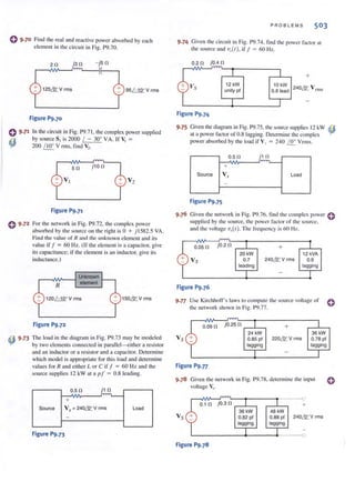
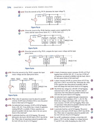
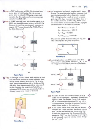
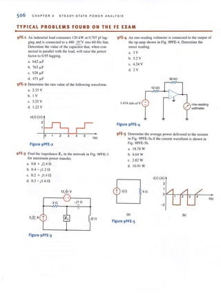

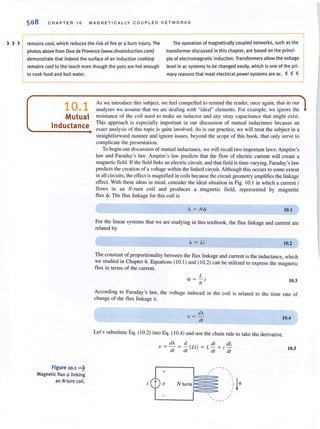
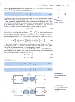
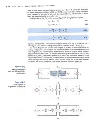
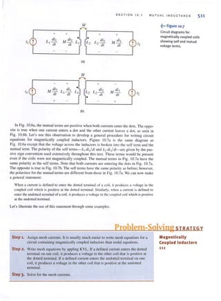
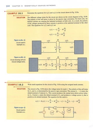
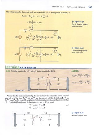
![•
514 CHAPTER 10 MAGN ETI CALLY COUPLED NETWORK S
EXAMPLE 10.3
•
The model of (he coupled circuit in the frequency domain is identical to that in the time
domain except for the way the clements and variables are labeled. The sign on the mutual
terms is handled in the same manner as is done in the time domain.
The two mutually coupled coils in Fig. 1O. ll a can be interconnected in four possible ways.
We wish to determine the equivalent inductance of each of the four possible interconnections.
SOLUTION Case I is shown in Fig. 10.llb. In this case
V = jwL,I + jwM I + jwL, [ + jwM I
= jwLcq l
where L,q = L, + L2 + 2M.
Case 2 is shown in Fig. 10.lle. Using KVL, we obtain
V = jwL ,1 - jwM I + jwL, [ - jwM[
= jwLeql
where L,q = L, + L2 - 2M.
Case 3 is shown in Fig. 10.l ld and redrawn in Fig. 10.lle. The two KYL equations are
V = jwL, [, + jwM[,
V = jwMII + jwL2I 2
Solving these equations for I, and I, yields
Using KCL gives us
where
V(L, - M)
I I =
jw(L,L, - M' )
V(L, - M)[ , = _c-'--'--_-'-_
- jw(L,L, - M')
, = " + [, =
V(L, + L, - 2M )
jw(L,L, - M' )
L]L2 - M2
L, + L, - 2M
V
jwL"'l
Case 4 is shown in Fig. 10. 11 f. The voltage equations in this case will be the same as
Figure 10.11.J.. those in case 3 except that the signs of the mutual terms will be negative. Therefore,
Circuits used in
Example 10.3.
(aj
LL2 - M2
L, + L, + 2M
"
jwM jwL2
./' '-.. _,!.,"rrn")
26----0 3 4
, V
L-------~+ -r_------~
(bj
/
/](https://image.slidesharecdn.com/basicengineeringcircuitanalysis9thirwin-160630150938/85/Basic-engineering-circuit-analysis-9th-irwin-536-320.jpg?cb=1719934140)
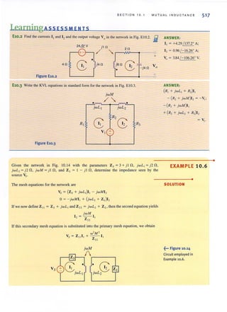
![518 CHAP TER 10 MAGN ET1 CA LLY CO U PLED NETWORKS
and therefore
which is the impedance seen by Vs. Note that the mutual term is squared, and therefore the
impedance is independent of the location of the dots.
Using the values of the circuit parameters, we find that
Vs = (3 + '1 + '2) + 1
I, J J j2 + 1 - j l
= 3 + j3 + 0.5 - jO.5
= 3.5 + j2.5 fl
LearningAss ESSM ENT
E10.4 Find the impedance seen by the source in the circuit in Fig. E 10.4. ~ ANSWER:
Z s = 2.25 / 20.9° fl.
j l n
r---vw--- -If--,./...---Iw--......-----,l
! j2n ,,, - j2n U,n
2n - jl n 2n
120&V
Figure E10.4
10.2
Energy
Analysis
j2n
t . f
We now perform an energy analysis on a pair of mutually coupled inductors, which will
yield some interesti ng relationships for the circuit elements. Our analysis will involve the
performance of an experiment on the network shown in Fig. 10.15. Before beginning
the experiment, we set all voltages and currents in the circuit equal to zero. Once the cir-
cuit is quiescent, we begin by letting the current ;1 (/ ) increase from zero (0 some value I I
with the right-side terminals open circuited. Since the right-side terminals are open,
;2(/) ;:::: 0, and therefore the power entering these terminals is zero. The instantaneous
power entering the left-side terminals is
[
eli,(t) ]
pet) = v,(t)i,(t) = L,-- i,(I)
ell
The energy stored withi n the coupled circuit al l, when i, (I) = I , is then
1', 1" Iv, (I )i, (I) dl = L,i,(I) di,(I ) = - L,/;
0 0 2
Continui ng our experiment, starting at time 11 ' we let the current ;2(1) increase from zero to
some value 12 at time 12 while holding ;1 (1) constant at I I. The energy delivered through the
right-side terminals is
1', 1t.v,(I)i,(I ) dl = L,i,(I) di,(I )
• 0](https://image.slidesharecdn.com/basicengineeringcircuitanalysis9thirwin-160630150938/85/Basic-engineering-circuit-analysis-9th-irwin-540-320.jpg?cb=1719934140)
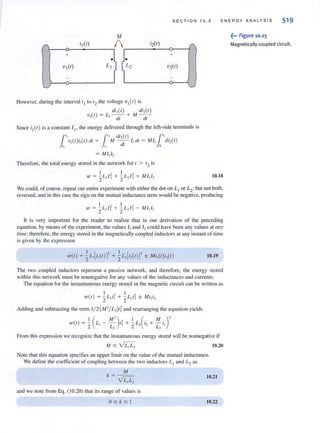
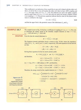
![522 CHAPTER 10 MAGNETICALLY COUPLED NETWORKS
Figure 10.18 .j..
Symbol for an ideal
transformer: (a) prima ry
and secondary currents
into the dots; (b) pri mary
current into, and
secondary current out of,
the dots.
and hence the total power into the device is zero, which means that an ideal transformer
is lossless.
The symbol we employ for the ideal transformer is showll in Fig. I0. 18a, and the corre-
sponding equalions are
10.28
The normal power flow through a transformer occurs from an input currcnt (iI) on the
primary (0 an ompul current (;2) on the secondary. This situation is shown in Fig. 1O. ISb,
and the corresponding equHtions arc
VI NI
'Vz Nz 10.29
Nli] = Nziz
Note that although the voirage, current, and impedance levels change through a (rans-
fonner, the power levels do not. The venical lines between the coils. shown in the figures,
represent the magnetic core. Although practical transformers do not use dots per se, they use
markings specified by the National Electrical Manufacturers Association (NEMA) that are
conceptuall y equi valent 10 the dots.
Thus. our model for the ideal transformer is specified by the circuit in Fig. 10. 18a and
the corresponding Eq. ( 10.28), or alternatively by the circuit in Fig. I0. 18b, toget her with
Eq. ( 10.29). Therefore, it is important to note carefully that our model specifies the equa-
tions as well as the relationship among the voilages, currents, and the position of the dots.
In other words, the eq uations are valid only for the corresponding circuit diagram. Thus,
in a di rect analogy to our discussion of the mutual inductance equations and their corre-
sponding circuit, if we change the direction of the current or voltage or the position of the
dots, we must make a corresponding change in the equations. The following material will
clarify this critical issue.
Consider now the circuit shown in Fig. 10. 19. If we compare th is circui t to that shown in
Fig. 1a. ISb, we f'ind that the direction of both the currents and voltages are the same. Hence
the equations for the network are
and
,.:--- 0----1"
Nt :Nz
it
.lllJ.
" --0--_---,
+ ' 2 +
'V t V2
r...../ Ideal tdeat
(a) (b)](https://image.slidesharecdn.com/basicengineeringcircuitanalysis9thirwin-160630150938/85/Basic-engineering-circuit-analysis-9th-irwin-544-320.jpg?cb=1719934140)
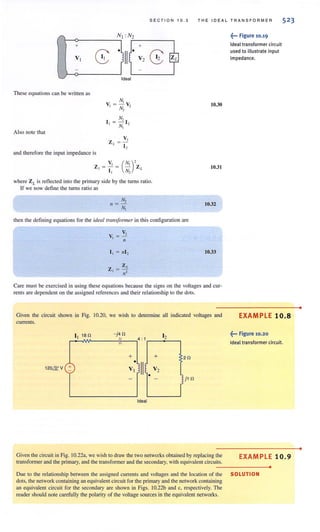
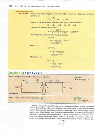
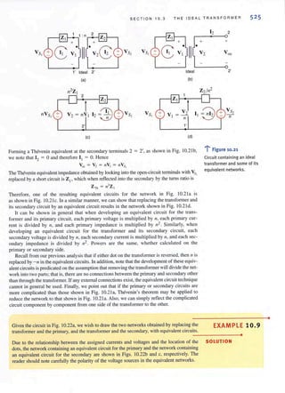
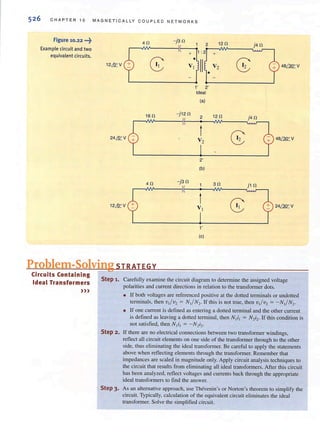
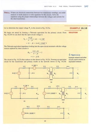
![•
528 CHAPTER 10 MAGN ETI CAL LY CO UPLED NETWORKS
Therefore, the voltage V0 is
-28.84 / -33.69'
V,~ 20-j5 (2)
~ 2.80 / 160.35' V
LearningAss ESS MEN IS
E10.8 Given the network in Fig. EtO.S, fonn an equivalent circuit for the transfonner and ANSWER:
secondary, and lise the resuhant network to compute I" I( = 13.12 / 38.66° A.
1 2 n -j2n 2 n
~~I ~~______-;I__--,1 :2r-~NV~-,
36&,V • II
•
12&' V
Figure El0.8 Ideal
El0.9 Given the network in Fig. EIO.9. [ann an equivalent circuit for the transformer and
primary. and use the resultant network to find Vo'
ANSWER:
V, ~ 3.12 / 38.66' V.
2n -j2n 4&'V
1: 2 ---0
+
•
II
•
12&' V 2n Vo
---0
Figure El0.9 Ideal
EXAMPLE 10.11 Determine Ii' 12 , Vi' and V2 in the network in Fig. 10.24.
•
SOLUTION The nodal equations at nodes I and 2 are
Figure 10.24 .••~
Circuit used in
Example 10.11.
10 - V,
2
V, - V,
] 2 + 2
V, - V,
--'-__..0' + 1
V,
2j
2 '
The transformer relationships are V2 ~ 2V I and I, ~ 212 , The first nodal equation yields
I, ~ 5 A and therefore 12 ~ 2.5 A. The second nodal equation, together with the constraint
equations specified by the transfonner, yields V, ~ V5 / 63' V and V, ~ 2V5 / 63' V.
2n
10&'V j2 n](https://image.slidesharecdn.com/basicengineeringcircuitanalysis9thirwin-160630150938/85/Basic-engineering-circuit-analysis-9th-irwin-550-320.jpg?cb=1719934140)
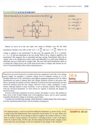
![•
530 CHAP TER 1 0 MAGNET I CA L L Y COUPLED NETW O RKS
•
SOLUTION Unaware of the extension cord connection, the line technician believesthat there isno volt-
age between points X and Z. However, because of the electrical connection between the two
homes, 7200 V nTIS exists between the two points, and the line technician could be seriously
injured or even ki lled if he comes in contact with this hjgh voltage.
Figure 10.25 ...~
Diagrams used
in Example 10.12
(voltages in rms).
10.5
Application
Examples
APPLICATION
EXAMPLE 10.13
II
120 V
II
X Y
7200 V OV 7200 V
Z
(a)
7200 V II
(b)
The following examples demonstrate several applications for transformers.
Considerthe problem of transporting 24 MWover a distance of 100 miles (160.9 km) using
a two-conductor Hne. Detennine the requisite conductor radius to achieve a transmission
efficiency of 95%, considering only the line resistance, if the line operates at <a) 240 V rms
..
_______-'o"'r"'(b) 240 kV rms. Assume that conductor resistivity is p = 8 X 10⁻⁸
nom.
•
SOLUTION a. At 240 V:
P 24M
1 = - = -- = 100 kA rms
V 240
If
T] = 95%,
1,,, = 0.05(24 M) = 1.2 MW = I' R](https://image.slidesharecdn.com/basicengineeringcircuitanalysis9thirwin-160630150938/85/Basic-engineering-circuit-analysis-9th-irwin-552-320.jpg?cb=1719934140)
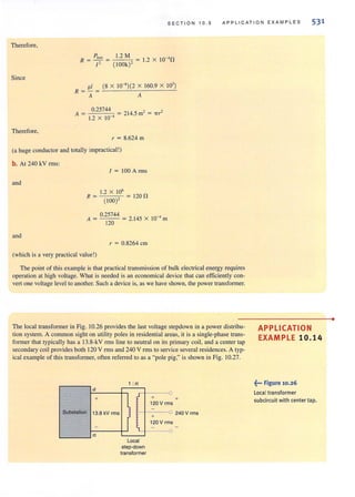
![•
53 2 CHAPTER 10 MAGN E TICALLY COUPLED N ET WORKS
Figure 10.27 ..i...
A residential utility
transformer.
(iStockphoto)
APPLICATION
EXAMPLE 10.15
•
Let us find the turns ratio necessary to produce the 240·V rms secondary voltage.
Assuming that the transfonner provides 200·A nns service to each of 10 houses, let us deter·
mine the minimum power rating for the transfonner and the maximum current in the primary.
•
SOLUTION
The turns ratio is given by
V, 240 1
,,= -=---=--
V, 13,800 57.5
If IHis the maximum current per household, then the maximum pri-
mary current is
I, = Ill, = 11(1011/) = 34.78 Arms
The maximum power delivered to the primary is then
S, = V, I, = ( 13,800)(34.78) = 480kVA.
Therefore, the transformer must have a power rating of at least 480
kVA.
Your electric toothbrush sits innocuously in its cradle overnight. Even though there are no
direct electrical connections between the cradle and the toothbrush, the internal batteries are
being recharged. How can this be?
SOLUTION Mutually coupled inductors is the answer! One coil is in the cradle and energized by an ac
source. The second coil is in the bottom of the toothbrush itself. When the toothbrush is
mounted in the cradle, the two coils are physically close and thus mutually coupled, as
shown in Fig. 10.28.
Let's investigate a reasonable design for these coils. First, we assume thal the coils are
poorly coupled with a coupling coefficient of k = 0.25. Second, the coil in the cradle is
driven at 120£2: V rIllS. Third, the coil in the toothbrush should generate 61.2:.. V at
100 mA nns in order to charge the battery. To keep the power "relatively" low, we will
limit the primary current to only 0.5 A nns. Finally, to simplify our analysis, we will
assume that 11and 12are in phase.
First we develop loop equations for OUf circuit, which are
VI = jwL ,I ] - jwMI 2
10.34
v, = jwMI , - jwL, I ,](https://image.slidesharecdn.com/basicengineeringcircuitanalysis9thirwin-160630150938/85/Basic-engineering-circuit-analysis-9th-irwin-554-320.jpg?cb=1719934140)
![SECTION 10.5 APPLICATION EXAMP L ES 533
Toothbrush
(al
Coil 2
VI
120~V rms
J.jwL2
(b)
where VI = 120I!!... V nTIS and Vz = 61!!... V rms. By defining a new variable a such that
L-z = a 2
L
we can eliminale L, in Eqs. (10.34). Hence,
V, = jwL, I, - jwkaL, I ,
V2 = jwkaL] I] - jwa?L]lz
Taking the ratio of each side of Eqs. (10.35), we can eliminate wand L,.
V, 120 I, - kal ,
- = - = 20 = -
V2 6 kal ] - a 2
12
10.35
if we now substitute the design parameter values listed above for 1]. 12and k and then solve
for "', we find
which yields
201,,,,' - (20k/ , + kI,)a + I, = °
a = {0.246
1.02
(We have used our restriction that I] and 12 are in phase to convert current phasors to
magnilUdes.) Choosing the smaller value for ", is the same as choosing a smaller L,. Hence,
this is the result we select since the resulting coil will require fewer turns of wire, reducing
cost, weight, and size. Next, using Eg. (10.35), we can solve for the product wL,.
V, = wL, (0.5) - w(O.25)(0.246)L,(O. I) = 0.494wL,
To investigate the effectof w on LI • we use the value for VIand the relationship between the
two inductors, for the given a .1n Table 10.1 , L, and L, have been calculated for a collection
of w values. Note that a 60-Hz excitation requires huge values for the inductances that are
completely impractical. Therefore, the table skips past the entire audible range (there's no
reason to have to listen to your toothbrush recharging) to 20 kHz. Here the inductance val-
ues are much more reasonable but still considerable. However, at 100 kHz, the total induc-
tance is just a few hundred microhenrys. These are very reasonable values and ones which
we will use.
12
+
Banery
V2 charger
-
..:-.
: Figure 10.28
The electric toothbrush:
(a) a nonartist's conceptual
drawing and (b) a circuit
schematic.](https://image.slidesharecdn.com/basicengineeringcircuitanalysis9thirwin-160630150938/85/Basic-engineering-circuit-analysis-9th-irwin-555-320.jpg?cb=1719934140)
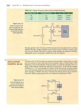
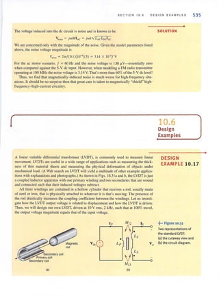
![536 C HAPTE R 1 0 MAG NET ICA LL Y COU PLE D NET WORKS
•
SOLUTION Typically, the primary winding of the LVDT is excited by an ac sinusoid in the range of
3 to 30 V rms at frequencies between 400 and 5000 Hz. Since we only need to measure the
output voltage directly with a voltmeter, no external load is necessary.
Figure 10.32 "'~
Coupling coefficients
for each secondary
winding and the coupling
difference. It is the differ·
ence that witl determine
the output voltage
magnitude.
The null position forthe rod is deadcenter between the secondary windings. In that posi-
tion the coupling between the primary and each secondary is identical, and the output volt-
age is zero. Should the rod move in either direction, the coupling will change linearly, as
will the output voltage magnitude. The direction of travel is indicated by the relative phase
of the output.
Our LVDT design begins with the circuit in Fig. IOJ Ib where the mutual coupling coeffi-
cient for each secondary winding varies as shown in Fig. 10.32. To create a bnearrelationship
between displacement and output voltage, we restrict the nominal travel to that portion of
Fig. 10.32 where the coupling coefficient is linear with displacement. Therefore, in this
design, 100% travel will correspond to a coupling coefficient of 0.8.
Applying KVL to the primary loop yields
10.36
At the secondary, the KVL equation is
2(jwLs)l s + jwMl3 l 1' - jwMl2 l p + Vo = a 10.37
With no load at the output, Is = aand Eqs. (10.36) and (1 0.37) reduce to
10.38
Solving these for the output voltage and recognizing that MIX = k1x[L/'Ls]0.5, we obtain
10.39
We can express the coupling coefficienLS for each secondary in terms of the percent of
travel.
{
Oo·oosxk 12 =
t .2
0.8
C
.!!!
g
" 0.6
"0
0
0> 0.4oS
C.
~
0
0.20
0
- 0.2 . .
fora < x < 100
for x < a kl) =
I
{
o.oosx
a
[k t2 - kI3J
~ /
V "
~
for - lOa < x < a
for x > a
V
1 I k I3"
k
/ 2 I
"< /
/ ) i1"
/ , J .~
.. , .. , , ,
- 200 - 150 - 100 - 50 o
Travel
50 100 150 200](https://image.slidesharecdn.com/basicengineeringcircuitanalysis9thirwin-160630150938/85/Basic-engineering-circuit-analysis-9th-irwin-558-320.jpg?cb=1719934140)
![SECTION 10.6 DE S IGN EXAM P LES 537
And, finally. assuming that the input voltage has zero phase angle, the output voltage can be
expressed as
JEs JEs 0
V, ~ V;, - [0.008x ] ~ V;, - [0.008x]1'2:
Lp Lp
0 < x < 100
10.40
V, ~ V;, {L,[- 0.008x] ~ V;, (L,[+0.008x] /- 180°
I~ I~
- 100 < x < 0
Note the phase angle difference for positive versus negative travel.
To complete our analysis, we mustdetermine a value for the secondary to primary induc-
tance ratio. At 100% travel, the magnitudes of the input and output voltages are equal and
k = 0.8. Using this information in Eq. (10040), we find that the inductor ratio must be
Lsi Lp = 1.25' = 1.5625.
To detennine actual values for the inductances, we must consider the input current we will
tolerate at the primary. We would prefer arelatively small current, because a large current would
require large-diameter wire in the primary winding. Let us choose a primary current of 25 rnA
rms with an excitation of 10 V nns at 2000 Hz. From Eq. (10.38), the primary inductance will
be
"in 10
L" = -w ]- p = 21r(2000)(0.025) ~ 31.8 mH
which yields a secondary inductance of
Ls ~ 1.5625Lp = 49.7 mH
The selection of the two inductances completes this design.
The next example illustrates a technique for employing a transformer in a configuration that
will extend the life of a set of Christmas tree lights.
The bulbs in a set of Christmas tree lights normally operate at 120 V rms. However, they
last much longer if they are instead connected to 108 V rms. Using a 120 V- 12 V trans-
former, let us design an autotransformer that will provide 108 V rms to the bulbs.
DESIGN
EXAMPLE 10.18
•
The two-winding transformers we have presented thus far provide electrical isolation SOLUTION
between primary and secondary windings, as shown in Fig. 1O.33a. It is possible, however,
to interconnect primary and secondary windings serially, creating a three-terminal device,
known as an autotransformer, as shown in Fig. 10.33b and represented in Fig. 10.33c.
As we shall see, this arrangement offers certain practical advantages over the isolated
case. Note that the three-terminal arrangement is essentially one continuous winding with
an internal tap.
To reduce the voltage from 120 V rms to 108 V rms, the two coils must be connected
such that their voltages are in opposition to each other, corresponding to a subtractive con-
nection (in Fig. 10.33b), as shown in Fig. 10.34. In this arrangement, the voltage across both
coils is
Vo ~ VI - V, = 120 - 12 ~ 108 Vmls
and the lights are simply connected across both coils.
•](https://image.slidesharecdn.com/basicengineeringcircuitanalysis9thirwin-160630150938/85/Basic-engineering-circuit-analysis-9th-irwin-559-320.jpg?cb=1719934140)
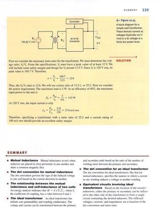
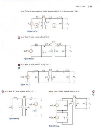
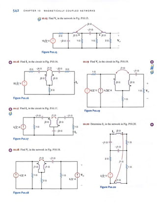
![546 C H A PTER 10 MAGN ETI CALLY COUPLED N ET WO RK S
0 10.41 The currents in the network in Fig. PI0.41 arc
known 10 be ;,(f ) = 10 co,(377f - 30") mA and
i:z{t) = 20 c05(3771 - 45°) mAo The inductances are
L, = 2 H, L, = 2 H, and k = 0.8. Delen"ine V,(f )
and V,(f).
!vi
; I (f)
/ ;2(f)
"+
J. +
•
V,(f) LI L2 V2(f)
Figure Pl0.41
o 10.42 Delcnnine the energy stored in the coupled inductors in
the circuit in PIO.4 1at I = I inS.
o 10·43 The currents in the magnetically coupled induclOfs
shown in Fig. PI 0.43 arc known to be
;,(f) = 8cos(377f - 20") mAand
;,(f) = 4 cos(377f - 50") rnA. The induclor values are
L, = 2H, and L, = I H, and k = 0.6. Delen"ine V,(f)
and V,(f).
,-------1"
+ +
•
VI(f) L,
Figure PlO.43
e 10·44 Determine the energy stored in the coupled inductors in
Problem 10.43 at I = I ms.
o 10·45 Find all currents and voltages in the network in
Fig. PI0.45.
1 : 2
I I 10 12
+ + 30
12.& V + V,
'II V2
• • ] j1 0
Ideal
Figure Pl0.45
10.46 Determine V" in the circuit in Fig. PI0.46.
1 n
24ill,: V
- j10
L---~ --o
Ideal
10.47 Determine I I' [ 2' VI i.U1d V2illihe network ill Fig. PIOA7. 0
I 0 I I 2: 1 12 iii-+
J +•
II12mV V, V, I 0
1·--
Ideal
Figure Pl0.47
10-48 Determine Vo in the circuit in Fig. PIOA8.
- jl0 +
'----~--<>
Ideal
Figure Pl0.48
10.49 Detenninc I I, 12• VI' and V2in the network in Fig. PJO.49. 0
2fl I,
- j l 0 j4 fl
Ideal
Figure Pl0.49
10.50 DCICnlline I I' ] 2- VI' and V2inlhc network in Fig. PIO.50. e
1 0
20
Figure Pl0.50](https://image.slidesharecdn.com/basicengineeringcircuitanalysis9thirwin-160630150938/85/Basic-engineering-circuit-analysis-9th-irwin-568-320.jpg?cb=1719934140)
![550 C H APTER 10 MAGNETICALLY CO UPLED NETWORKS
0 10.66 Determine the input impedance seen by the source in the network shown in Fig. PIO.66.
~
4 : 1 11 2 : 1,-___--,
,---.1
20
1'01'---., 4 0 ,"
Vs + Oil!0
Ideal
Figure P10.66
10.67 In the network shown in Fig. PI 0.67, detennine the value
of the load impedance for maximum power transfer.
30
-j2 0
1 12I 1: 2
+ +
0
II
0
24,:Q:y VI V2
Ideal
Figure P10.67
10.68 In the network shown in Fig. PI 0.68, detennine the value
of the load impedance for maximum power transfer.
-J40
40
j20
r
Ideal
10.70 Determine Vj' in the circuit in Fig. 10.70.
,--NV-...fY'YTl..--,1 : 2r--.NV-~'--o
1 0 j1 fl 10 +
o
II 0
Ideal
Figure P10.70
10.71 Given that Vo = 48 (300
V in the circuit shown in
Fig. PIO.7l, detennine Vs'
I I so - jSO
12
30
- j20
1 12I 1 : 2
:2
I +
--0
+ +
0
II12~V VI V2
0
Figure P10.68
o 10.69 The output stage of an amplifier in an old radio is to be
matched 10 the impedance of a speaker, as shown in
Fig. PIO.69. If the impedance of the speaker is 8 nand
the amplifier requires a load impedance of 3.2 k!1,
detennine the turns ratio of the ideal transfonncr.
'"'-]irQ:]Ideal
Figure P10.69
+
0
Vs VI
Figure P10.71
+
II! V2
24 fl
Vo
0
' - - - - -..--0
Ideal
10.72 Determine [s in the circuit in Fig. PIO.72.
,---'-_-I!---,1 : 2r-~¥----'
- j2 fl
1 0
20
o II 0
j10
Ideal
Figure P10.72
0 10.73 In the network in Fig. PIO.73, if [ I = 4 f§:... A, find V...
~
,--,IW'----,2 : 1 II
40 ,"
o 11
10
- J10
Vs
Ideal
Figure P10.73
20
1 0
II
1:2,---If----,
olll 0
Ideal
- j40
ao](https://image.slidesharecdn.com/basicengineeringcircuitanalysis9thirwin-160630150938/85/Basic-engineering-circuit-analysis-9th-irwin-572-320.jpg?cb=1719934140)
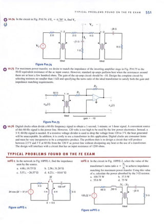
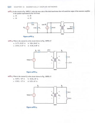
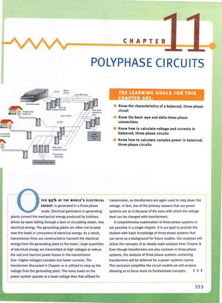
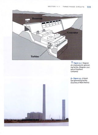
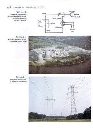
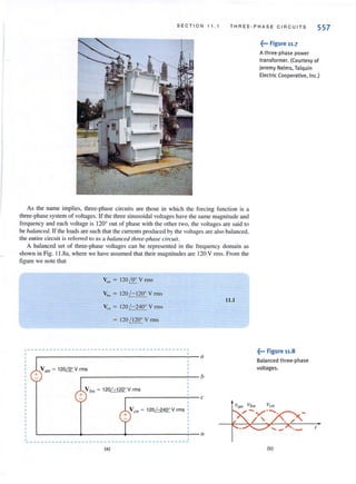
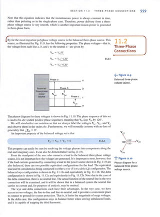
![560 C H A PTER 11
Figure 11.11 ...::"
Wye (Y)·connected loads.
Figure 11.12 ---i-
Delta (~) ·co n n ected loads.
V all
-+
11.3
Source/load
Connections
a I"
Vb"
b
-+
V eil
I"
Figure 11.13 --i'
Balanced three·phase
wye-wye connection.
P O LYPH ASE C IR CUI T S
------ - --- - ----- - -----.
a --~: ---------------------,
b-+--,
a Zy l--~
b Zyl--'"
C Zyl--'"
c ---+------'
/I __-'-__________J
II --~--------------------~
Load1_ _ ____________ _
I Load :
'- - - - - - - - - - - - - - - - - - - - --
(a) (b)
- - -- --- - ------ - - -- - -- ---- - ---- - ---, ,
a --~_<I---~
a- +----....,o..
b-'---.... Zt;
b--+-----l
c __.:.-4___-1
c --------~
Load Load
1- _____________ ..! I______ ____________ ..!
(a) (b)
Since the source and the load can each be connected in either Y or a, three-phase balanced
circuits can be connected Y- Y, Y-u,u-Y, or u-u.Our approach to the analysis of ali of these
circuits will be "Think Y"; therefore, we will analyze the Y- Y connection first.
BALANCED WYE-WYE CONNECTION Suppose now that both the source and load are con-
neeted in a wye, as shown in Fig. 11 .13. The phase voltages with positive phase sequence are
Vim = Vp~
Vb, = Vp / - 120'
Veil = Vp !+ 120°
11.13
where ~, . the phase voltage, is the magnitude of the phasor voltage from the neutral to any
line. The line-lo-Iine or, simply, line voltages can be calculated using KVL; for example.
= VpLSr. - Vp/ - 120'
= V - V [_.!. _j v'3]p p 2 2
= Vp[~ + j '; ]
= v'3V /30'I'](https://image.slidesharecdn.com/basicengineeringcircuitanalysis9thirwin-160630150938/85/Basic-engineering-circuit-analysis-9th-irwin-582-320.jpg?cb=1719934140)
![SECT I ON 1 1 . 3 SO U R CE / LOAD CONN E C TI ONS
VCIl Vetl
V ab
(a) (b)
The phasor addition is shown in Fig. 11.1 4a. [n a similar manner, we obtain the set of line-
lo-Iine voltages as
Vo' = V3 Vp/ 30"
Vb< = V3 Vp / - 90"
V", = V3 Vp/-21O"
11.14
All the line voltages together with the phase voltages are shown in Fig. 11.1 4b. We will
denote the magnitude of the line vohages as VL , and therefore, for a balanced system,
11.15
Hence, in a wye-connected system, the line voltage is equal to V3 times the phase voltage.
As shown in Fig. 11.13, the line current for the a phase is
11.16
where Ib and Ie have the same magnitude but lag Ia by 1200
and 240°, respectively.
The neutral current In is then
I" = (1" + I , + I,) = 0 11.17
Since there is no current in the neutral, this conductor could contain any impedance or it
could be an open or a short circuit, without changing the results found previously.
As illustrated by the wye- wye connection in Fig. 11 .13, the current in the line connecting
the source to the load is the same as the phase current flowing through the impedance Zy.
Therefore, in a wye- wye c01lnectioll,
h = Iy 11.18
where If. is the magnitude of the line current and /y is the magnitude of the current in a wye-
connected load.
Although we have a three-phase system composed of three sources and three loads, we
can analyze a single phase and use the phase sequence 10 obtain the voltages and currents in
the other phases. This is, of course, a direct result of the balanced condition. We may even
have impedances present in the lines; however, as long as the system remai ns balanced, we
need analyze only one phase. If the line impedances in lines G, h, and c are equal, the system
will be balanced. RecalJ that the balance of the system is unaffected by whatever appears in
the neutral line, and since the neutral line impedance is arbitrary, we assume that it is zero
(i.e., a short circuit).
~... Figure 11.14
Phasor representation of
phase and line voltages in a
balanced wye- wye system.
[hint]
Conversion rules
t!....=~ + 30"
Vab = v'3 Van](https://image.slidesharecdn.com/basicengineeringcircuitanalysis9thirwin-160630150938/85/Basic-engineering-circuit-analysis-9th-irwin-583-320.jpg?cb=1719934140)
![•
•
562 CHAP TER 11 POLYPHASE CIRCU IT S
EXAMPLE 11.1
•
SOLUTION
[hint]
The phase of
Van = ~ = t:!H - 30°
EXAMPLE 11.2
•
An abc-sequence three-phase voltage source connected in a balanced wye has a line volt-
age of VI/h = 208 j- 30° V rms. We wish to determine the phase voltages.
The magnitude of the phase voltage is given by the expression
208
Vp = Y3
= 120 V rms
The phase relationships between the line and phase voltages are shown in Fig. 11.14. From
this figure we notc that
VII/I = 120 / - 60° V rms
Vb/l = 120 / - J80o Yrms
Vel! = 120 !+600
V nns
The magnitudes of these voltages are quile common, and one often hears that the electric
service in a building. for example. is three-phase 208/ 120 V rms.
A three-phase wye-connected load is supplied by an abc-sequence balanced three-phase
wye-connected source with a phase voltage of 120 V rms. If the line impedance and load
impedance per phase are 1 + j 1 nand 20 + j Ion. respectively. we wish to determine the
value of the line currents and the load voltages.
SOLUTION The phase voltages are
[hin t]
& =&- 120°
& =& + 120°
Figure 11,15 "':i
Per·phase circuit diagram
for the problem in
Example 11.2.
V = 120 100 Vrmsall ~
Vb" = 120 / - 120° V rms
y,. = 120 /+ 120° V rms
The per-phase circuit diagram is shown in Fig. 11 .15. The line current for the a phase is
I _ _1_20-,~=0~0
aA - 21 + j ll
= 5.06 / - 27.65° A rms
The load voltage for the a phase, which we call VAN, is
V AN = (5.06 / - 27.65°)(20 + j lO)
= 113.15 / - 1.08° V rms
InA 1 fl j1 fl
ao-~~~~" . '. :·~-c A
20 fl
j10 fl
116---------6 N](https://image.slidesharecdn.com/basicengineeringcircuitanalysis9thirwin-160630150938/85/Basic-engineering-circuit-analysis-9th-irwin-584-320.jpg?cb=1719934140)
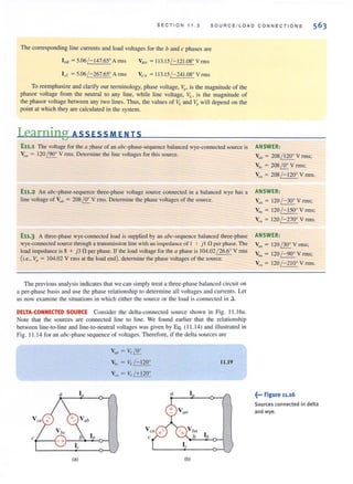
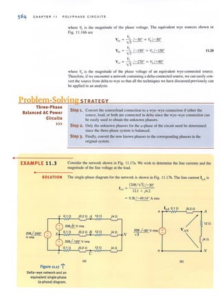
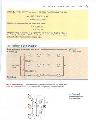
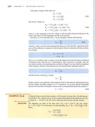
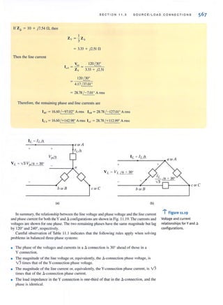
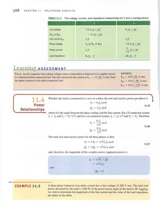
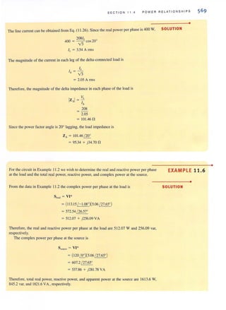
![•
•
570 C HA PTER 11 P O LYP H AS E C I RC U ITS
EXAMPLE 11 .7
•
A balanced three-phase SOurce serves three loads as follows:
Load I: 24 kW at 0.6 lagging power factor
Load 2: 10 kW al unity power faclor
Load 3: 12 kVA at 0.8 Icading power faclOr
If the line vollage a l the loads is 208 V fillS at 60 Hz, we wish to dctcnnine the line current and
the combined power factor of the loads.
SOLUTION From the data we find that
[hint)
The sum of three complex
powers
SIoMS = 51 + S2 + 53
EXAMPLE 11.8
•
SOLUTION
[hint)
Recall that the complex power
for all three lines is
S lint = 3/~Zline
Therefore,
S, = 24.000 + )32,000
S2 = 10,000 + )0
S, = 12,000 (- 36.9° = 9600 - )7200
S'oo' = 43,600 + j24.S00
= 50,160 ( 29.63° VA
IS'o,dl1 = - -
L V3VL
50,160
= 20SV3
IL = 139.23 A mlS
and the combined power factor is
p f]031l = cos 29.63°
= 0.S69 lagging
Given the three-phase system in Example 11.7, let us determine the line voltage and power
factor at the source if the line impedance is Z';ne = 0.05 + j O.02 n.
The complex power absorbed by the line impedances is
S tine = 3(Rlinc/i + jXlifllJ D
= 290S + j 1l 63 VA
The complex power delivered by the source is then
= 43,600 + j 24,SOO + 2908 + j ll63
= 53,264 ( 29. 17° VA
The line voltage at the source is then
S5
V =--
L, V3 IL
= 220.87 V rillS
and the power factor at the source is
pfs = cos 29.17°
= 0.873 lagging](https://image.slidesharecdn.com/basicengineeringcircuitanalysis9thirwin-160630150938/85/Basic-engineering-circuit-analysis-9th-irwin-592-320.jpg?cb=1719934140)
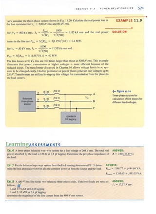
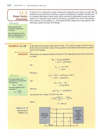
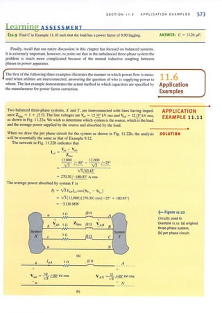
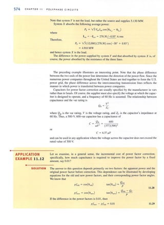
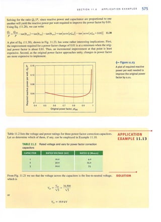
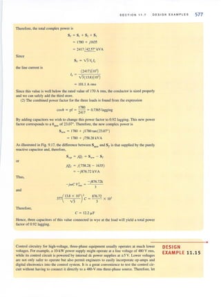
![578 CHAPTER 11 POLYPHASE CIRCUITS
us design a low-power. three-phase emulator that simulates a three-phase system at low
voltage and low cost and provides a test bed for the control circuitry. The emulator should
generate proper phasing but with a magnitude that isadjustable between I and 4 volts peak.
..- - - - - --
SOLUTION Our design, shown in Fig. 11 .25, will consist of three parts: a magnitude adjustment, a phase
angle generator, and a phase B generator. The ac input is a 60-Hz sine wave with a peak of
about 5 V. This voltage can be generated from a standard 120 V rms wall outlet using a step-
down transformer with a turns ratio of
Figure 11.25 •••~
Ablock diagram for a three·
phase emulator.
120V2
11 = - -- =34:1
5
Magnitude
adjustor
+
Phase
angle
generator +
Phase VBN
generator
+
The potcmiomClcr circuit shown in Fig. 11.26a can be used to provide magnitude adjust-
ment. Resistors R, and R, provide the voltage limits of I and 4 V. We can use simple volt-
age division to determine the relationships between Rio R2• and Rp. When the pot's wiper
arm is at the bottom of the pot in Fig. I1.26a, we have
11.31
and when the wiper is at the top,
11.32
Solving Eqs. (11.31 ) and (11.32) yields the requirements that R, = R, = Rel3. To obtain
values for these resistors we must simply choose one of them. We know that resistors are
available in a wide variety of values in small increments. Potentiometers on the other hand
are not. Typical potentiometer values are 10,20, 50, 100, 200, 500, ... IOk ... lOOk, 200k,
500k, ... up to aboUl 10 MD. Since the potentiometer offers fewer options, we will choose
its value to be 10 kf1, which yields R, = R, = 3.3 kfl-a standard resistor value. We will
set VI as the phase voltage ~N.
Next we consider the phase angle generator. Since capacitors are generally smaller phys-
ically than inductors, we will use the simple RC network in Fig. 11 .26b to shift the phase of
VI. Assigning a phase angle of 0° to VI' we know that the phase of V2 must be between 0
and - 90 degrees. Unfortunately, in order to generate VeN we need a phase angle of +120°.
If we create a phase angle of - 60° and invert the resulting sine wave, we will produce an
equivalent phase angle of +120°! The inversion can be performed by an inverting op-amp
configuration. To produce a -60° phase angle at V2 requires
wCR, = tan(600) = 1.732 R,C = 4.59 X 10-'
We will choose a standard value of 120 nF for C, which yields R, = 38.3 kn. This is a stan-
dard value at I%tolerance. Using these values. V2 will be
v - V [ I ] - ~ / -60°
,- , I + jwCR, - 2.0
11.33](https://image.slidesharecdn.com/basicengineeringcircuitanalysis9thirwin-160630150938/85/Basic-engineering-circuit-analysis-9th-irwin-600-320.jpg?cb=1719934140)
![S E CT ION 11. 7 D E SIG N E X AMP L ES 579
5 sin (wI) V +
(a)
+
R3
VI
1
jwC
+
R" ..---0
+
Vz
+
(b)
RS
+
o-------+-------------------~~----------~o
(e)
R6
+
VAN R7
+
VeN
(d)
+
From Eq. (11 .33) we see thai our inverter should also have a gain of 2 to restore Ihe mag-
nitude of V2. The complete phase angle generator circuit is shown in Fig. 11 .26c, where
R, = 10 kf1 and R, = 20 kf1 have been chosen 10 produce the required gain. Now V, is
used to represent YeN' The additional unity gain buffer stage isolates the resistances asso-
ciated with the inverter from the R-C phase generator. That way the inverter will not alter
the phase angle.
Finally, we must create the phase voltage VSN ' Since the sum of the three-phase voltages
is zero, we can write
The simple op-amp summer in Fig. 11.26d will perform this mathematical operation. For
the summer
VIIN = - [:;]VAN - [::]VCN
We require R6 = R7 = Rg. Since we are already using some IO-kn resistors anyway, we
just use three more here. The complete circuit is shown in Fig. 11.27 where one more unity
gain buffer has been added al the potentiometer. Thi, one isolates the R-C phase angle
generator from the magnitude adjustment resistors.
~••• Figure 11.26
Subcircuits within the three-
phase emulator: (a) the
magnitude adjustor. (b) the
R-eportion of the phase
angle generator. (c) the
complete phase angle
generator, and (d) the
generator for phase VaN.](https://image.slidesharecdn.com/basicengineeringcircuitanalysis9thirwin-160630150938/85/Basic-engineering-circuit-analysis-9th-irwin-601-320.jpg?cb=1719934140)
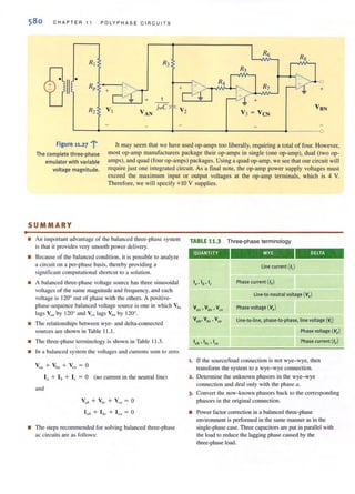
![582
~ 11.14
0 11•15
0 11.16
El
C H A PTER 11 PO LY PHA S E CI R CU IT S
In a three-phase balanced deila-delta system. the source
has an abc-phase sequence. The line and load imped-
ances are 0.5 + O. li nand 10 + is n. respectively.
If V,n = 11 5 ( 300
V rms. fi nd the phase voltage of
the sources.
An abc-sequence balanced Ihrec-plmse wye-connected
source supplies power 10 a balanced wye-connected
load. The line impedance per phase is J + j O 0 , and
the load impedance per phase is 20 + i 20 n . If the
source line voltage V(,,, is 100iQ: V fill S, finclthc line
currents.
An a bc-sequence set of voltages feeds a balanced
three-phase wye- wye system. The line and load
impedances are 1 + i l nand 10 + i lO n .
respectively. If the load vollage 0 11 the 0: phase is
V AN = 110 / 300
V rms, determine the line voltages of
the inpul.
~ 11.17 In a balanced three-phase system the source has an abc-
'¥' phase sequence and is connected in della. There arc two
loads con nected in pl.lrallel. Load I is connected in wye
and has a phase impcdance of 6 + )2 n.Load 2 is con-
nected in della and has a ph<lse impedance of 9 + ) 3 n.
The line impedance is 0.6 + ) 0.2 n.Determine the
phase vollages of the source if the current in the a phase
of load I is IAN, = 10 / 300
A rills.
o 11.18 In a b.llance three-phase wye-wye system. the source is
an abc-sequence set of voltages. The load voltage on the
a phase is VAN = 11 0 / 80° V nns, Zlinc = I + ) 1.4 n,
and Zlo::ad = 10 + ) 13 n.Determine the input sequence
of the Iinc-to-neutral vollages.
0 11.19
0 11•20
0 11•21
0 11
•
22
~
0 11•23
B~
In a balanced three-phase wye- wye system. the source
is an abc-sequence set of voltages. The load voltage
on the a phase is V AN = 120 / 60° V rms.
Zlin~ = 2 + ) 1.4 n, and Zload = 10 + ) Ion.
Determine the input voltages.
In a balanced three-phase wye- wye system. the source
is an abc-sequence set of voltages. Z1in~ = I + ) I fl.
Zload = 14 + ) 12 fl, and the load voltage on the a
phase is VAN = 440 / 30° V rms. Find the line
Voltage Vuh,
A balanced abc-sequence of voltages feeds a balanced
three-phase wye-wye system. The line and 10'ld imped-
ance are 0.6 + i O.9 n and 8 + i l2 n , respectively. The
load voltage on the a phase is VAN = 11 6.63 L.!...Q:. V rms.
Find the line voltage V I/b'
In a balanced three-phase wye- wye system. the load
impedance is 8 + ) 4 fl. The source has phase sequence
abc and VUII = 120 !St.. V nns. If the load voltage is
V AN = 111 .62 / - 1.33° V rillS, determine the line
impedancc.
In a balanced three-phase wye- wye system. the
lOtal power loss in the li nes is 400 W.
V AN = 105.28 / 3 1.56° V rms and the power factor
of the load is 0.77 lagging. If the line impedance is
2 + ) 1 n.determine the 10'ld impedance.
11.24
11.25
In a balanced three-phase wye- wye system, the
source is an abc-sequence set of voltagcs and
Vim = 120 / 40° V rms. If the a-phase line current and
line impedance are known to be 7.1 0 / - 10.28° A rms
and 0.8 + ) 1 fl, respectively, find the load impedance.
III a balanced three-phase wye-wye system. the load
impedance is 20 +) 12 n.The source has an abc-phase
sequence and V(III = 120 /.!!.° V nus. If the load voltage
is V AN = 111.49 /- 0.2° V rms, determine the
magnitude of the line currenl if the load is suddenly
short-circuited.
11.26 In a balanced three-phase wye-wye system, the load
impedance is 10 +) 1 fl. The source has phase
sequence abc and the line voltage V ab = 220 f]Q0V
rills. If the load voltage V AN = 120 /520V rms,
determine the line impedance.
11.27 An abc-phase-sequcnce three-phase balanced
wye·connected 60- Hz source supplies a balanced
dclta- connected load. The phase impedance in the
load consists of a 20-fl resistor series with a 20-1l1H
inductor. and the phase voltage at the source is
VI", = 120 f]Q0V rms. If the line impedance is zero.
find the line currents in the system.
11.28 In a three-phase balanced system, a delta-connected
source supplies power to a wye-connected load.
If the line impedance is 0.2 + ) 0.4 fl, the load
impedance 3 + )2 fl , and the source phase voltage
Vllb = 208 fJst V rms, find the magnitude of the line
voltage at the load.
11.29 In a balanced three-phase wye-wye system. the
source is an abc-sequence set of voltages and
11·30
11·31
11·32
11·33
Vim= 120 LJ5!.0V rills. The load voltage on the a
phase is 110 LJ5!.0V rillS, and the load impedance is
16 + ) 20 n. Find the line impedance.
In a balanced three-phase wye- wye system, the
source is an abc-sequence set of voltages and
Vim = 120 ~o V rms. If the a-phase line current
and line impedance are known to be 6 illoA rms
and I + ) 1 11, respectively. find the load impedance.
An abc-phase sequence three-phase balanced
wye-connected source supplies a balanced delta-
connected load. The impedance per phase in the delta
load is 12 +)6 n. The line voltage at the source is
V ab = 120 V3 ~o V nllS. If the line impedance is 7..ero.
lind the line currents in the balanced wye-delta system.
In a balanced three-phase delta-wye system. the source
has an a bc-phase sequence. The line and load imped-
ances are 0.6 + )0.3 nand 12 + )7 fl, respectively.
Ir the line current l ilA = 9.6 / -20° A rillS, determine
the phase voltages of the source.
In a three-phase balanced system, a delta-connected
source supplies power to a wye-connected load. If the
line impedance is 0.2 + ) 0.4 fl, the load impedance
6 + ) 4 11, and the source phase voltage V I/Ii = 2 10 ~o
V nllS, find the magnitude of the line voltage at the load.
o
o
o
o
o
o
o
o](https://image.slidesharecdn.com/basicengineeringcircuitanalysis9thirwin-160630150938/85/Basic-engineering-circuit-analysis-9th-irwin-604-320.jpg?cb=1719934140)


![SECT I ON 12.1 VARI ABLE FREQUENCY - RESPONSE ANALYS I S
593
1.0
0- 0.8
8
x 0.6
c
.,. 04
C!J .
0.2
flo Ii-IIOL-_________________________
10 100 1 k 10 k 100 k 1 M
Frequency (Hz)
o-----j
C in RO
+ + +
'VS(I) R in 'Vin(l)
1000Vin(l)
CO 'VO(I)
0
R in = 1 MO Cin = 3.18 nF Ro ~ 100 n Co ~ 79.58 nF
(a)
o-----j
l /SCin Ro
0
+ + +
VS(s) R in V in(S) Vo(s)
1000Vin (,") 1/SCo
0
(b)
that portion of the plot where the gain is constant and is bounded by two points, which we
will refe r to as fLO and J;.n. Notice once again that the frequency axis is a log axis and, thus,
the frequency response is displayed on a semilog plol.
A model for the amplifier described graphjcally in Fig. 12.6 is shown in Fig. 12.7a with
the frequency-domain equ ivalent circuit in Fig. 12.7b.
If the input is a steady-state sinusoid, we can use frequency-domain analysis to tind the gain
G (. ) = V,,(jw)
" jW Vs(jw)
which with the substitution s =:: jw can be expressed as
Usi ng voltage di vision, we find that the gain is
V,,(s) V;,,(s) V,,(s) [ R;" ] [ l/ sC,, ]
G"(s) = --- = - --- = ( 1000 )
V, (s) Vs(s ) V;"(s) R;" + I/ sC;" R" + 1/ £ "
or
~••• Figure 12.6
Amplifier frequency-response
requirements.
~••• Figure 12.7
Amplifier equivalent network.](https://image.slidesharecdn.com/basicengineeringcircuitanalysis9thirwin-160630150938/85/Basic-engineering-circuit-analysis-9th-irwin-615-320.jpg?cb=1719934140)
![594 CHAPTER 12 VARIABLE-FREQUE NCY NETWORK PERFORMANCE
Figure 12.8 "'t
Exact and approximate
amplifier gain versus
frequency plots.
1.0
0.8
0"
0
~ 0.6
x
c 0.4'iij
CD
0.2
0
f HI
10 100 1 k 10 k 100 k 1 M
Frequency (Hz)
Using the element values in Fig. 12.7a.
[ s] [40,00011" ]
Go(s) = s + lOOn ( 1000) s + 40,0001T
where IDOTI and 40,OOO7T arc the radian equivalents of 50 Hz and 20,000 Hz. respectively.
Since s = jw. the network function is indeed complex. An exact plot of GI){s) is shown in
Fig. 12.8 superimposed over the sketch of Fig. J2.6. The exact plot exhibits smooth transi-
tions at fLO and fHI; otherwise the plots match fairly well.
Let us examine our expression for G'/}(s) more closely with respect to the plot in Fig. 12.8.
Assume that f is well within the midband frequency range; that is.
};.o « f « f,"
or
100." « lsi « 40,000"
Under these conditions, the network function becomes
or
G,,(s) = 1000
Thus, well within midband, the gain is constant. However, if the frequency of excitation
decreases loward .ha. then lsiis comparable to IOO'lT and
G"(s) '" [ s ]( 1000)
s + 100"
Since RinCin = t/ IDOn, we see that Cin causes the rolloff in gain at low frequencies.
Similarly, when the frequency approaches Jill, the gain rolloff is due 10 Co'
Through this amplifier example. we have introduced the concept of frequency-dependent
networks and have demonstrated that frequency-dependent network performance is caused
by the rC<lcti vc elements in a network.
NETWORK FUNCTIONS In the previous section, we introduced the tcrm vo!wge gain,
G.v(s) . This term is actually only one of several network functions, designated generally as
H(s), which detlne the ratio of response to input. Since the fu nction describes a reaction due
to an excitation at some other point in the circuit, network functions are also called rransfer
jIlJlcriolls. Furthermore, transfer functions arc not limited to voltage ratios. Si nce in electrical
networks inputs and outputs can be either voltages or currents, there are four possible net-
work functions, as listed in Table 12. 1.
There are also driving poimfilJlcrioJ/s, which are impedances or admittances defi ned at a sin-
gle pair of terminals. For example, the input impedance of a network is a driving point function.](https://image.slidesharecdn.com/basicengineeringcircuitanalysis9thirwin-160630150938/85/Basic-engineering-circuit-analysis-9th-irwin-616-320.jpg?cb=1719934140)
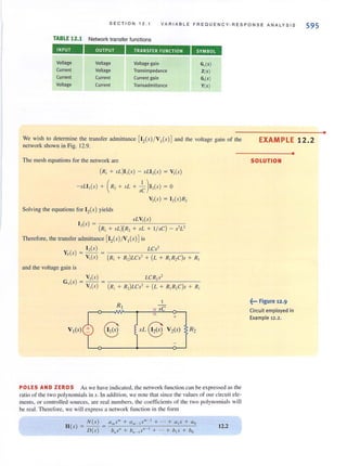
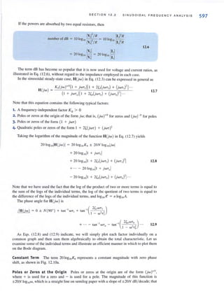
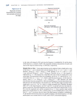
![S E CT I ON 12 . 2 SINUSOIDAL F R E OU E NCY ANALYSIS 599
2 3 4 56 7891 2 3 4 56 789 10
iIi 0
"-W
"0
.'l - 6'c
'"rn
:;
- 12
- 18
- 20
+18
iii'
:£. + 12
w
"0
.'l
'c
'"~ +6
dB ~ 20109,,1(1 + j WT)- '1
+::---~--.;;.- .;:..- - - - -,- - - - - - - - - - - 0
dB' tb = tan-1Wi
. , 'l. - - 20 dB/decad_'2o
0.2 0.5 1.0 2.0
WT (radls)(L09 scale)
(a)
dB ~ 20 109"I( 1 + jWT)1
q, = tan-1Wi
4.0 10
30
o
0.1 0.2 0.5 1.0 2.0 4.0
WT(rad/s)(L09 scale)
(b)
10
Quadratic Poles or Zeros Quadratic poles or zeros are of the form I + 2~(jWT ) +
(jwr )2. This teml is a function not only of w. but also of the di mensionless lenn ~, which is
called the damping ratio. If ~ > I or ~ = I. the roots are real and unequal or real and equal.
respectively, and these two cases have already been addressed. If ~ < I. the roots are complex
conjugates, and it is this case that we will examine now. Following the preceding argument for
a simple pole or zero. the log magnitude of the quadratic factor is 0 dB for wr « I,
ForwT » I.
2010g ,oll
and therefore. for W'T » I, the slope of the log magnitude curve is +40 dB/ decade for a
quadratic zero and - 40 dB/ decade for a quadratic pole. Between the two extremes. W'T « I
and Wi » I, the behavior of the function is dependent on the damping ratio ~. Figure 12. 12a
illustrmes the manner in which the log magnitude curve for a quadratic pole changes as a func-
tion of the damping ratio. The phase shift for the quadratic factor is tan-1 2~w'T/[ I - (wr)2].
The phase plot for quadratic poles is shown in Fig. 12. 12b. Note that in this case the phase
changes from 0° at frequencies for which Wi « Ito - 180° at frequencies for which W'T » I.
For quadratic zeros the magnitude and phase curves are inverted; that is, the log magnitude
curve has a slope of +40 dB/ decade for WT » I. and the phase curve is 0' for WT « I and
+ 180' for WT » I.
~.., Figure 12.11
Magnitude and phase plot (a)
for a simple pole, and (b) for
a simple zero.](https://image.slidesharecdn.com/basicengineeringcircuitanalysis9thirwin-160630150938/85/Basic-engineering-circuit-analysis-9th-irwin-621-320.jpg?cb=1719934140)
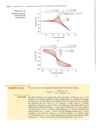
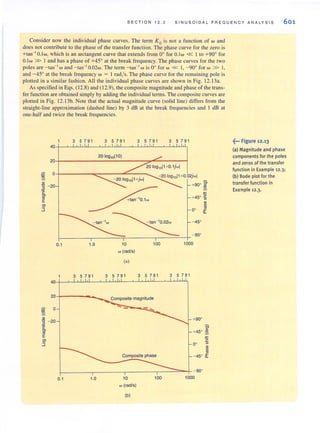
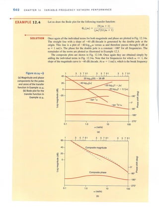
![•
C H APTER 12 VA RI A B L E - FR EQU EN CY N ET WORK PERFORM A N C E
EXAMPLE 12.5 Ve wish to generate the Bode plot for the following transfer function:
25jw
G,(jW)=(. +0 5)[(')' 4'JW . JW - + JW + 100]
•
SOLUTION Expressing this function in standard form, we obtain
Figure 12.15 -.~
Bode plot for the tran sfer
function in Example 12.5 .
0.5jw
G,(jW) = (2jw + 1)[(jw/ I0)' + jw/25 + I]
The Bode plot is shown in Fig. 12. 15. The initial low-frequency slope due to the zero at the
origin is +20 dB /decade. and this slope intersects the O-dB line at w = I / Ko = 2 rad/s. At
w = 0.5 rad/s the slope changes from +20 dB /decade to 0 dB /decade due to the presence
of the pole with a break frequency at w = 0.5 rad/s. The quadratic term has a center
frequency of w = 10 rad/s (i.e., T = 1/ 10). Since
and
then
I
2' T = -
, 25
.. = 0.1
~ = 0.2
Plotting the curve in Fig. 12.12a with a damping ratio of { = 0.2 at the center
frequency w = 10 rad/s completes the composite magnitude curve for the transfer
function.
The initial low-frequency phase curve is +90°. due to the zero at the origin. This curve
and the phase curve for the simple pole and the phase curve for the quadratic term, as
defined in Fig. 12. 12b, are combined to yield the composite phase curve.
10
"-
20
o
~ - 20
2
'c
'"~ - 40
3 57 9 1 3 5 79 1 3 5 791
I I
____ _ _ _ ____ .J __ _ -J -- --
I
--1--_"'"
3 5 7 9 1
c;
ID
"-
~
"'+90 3l
.."'o a.
--- - 90
~-------.---------r--------~~~--~ -lBO
0.01 0.1 1.0 10 100
'" (rad/s)](https://image.slidesharecdn.com/basicengineeringcircuitanalysis9thirwin-160630150938/85/Basic-engineering-circuit-analysis-9th-irwin-628-320.jpg?cb=1719934140)
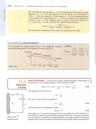
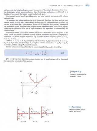
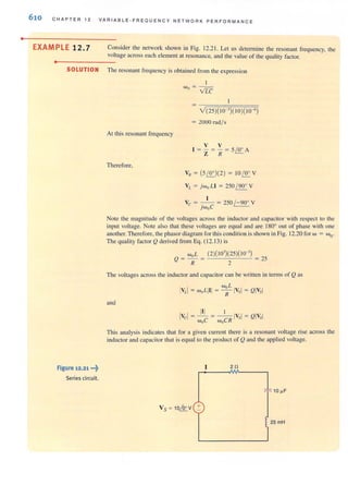
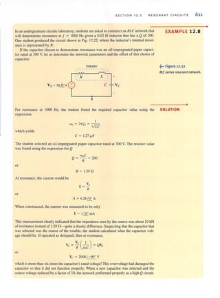
![612 CHAPT ER 12 VAR IABLE·FREQUEN CY N ETWORK PERFQRMANCE
Learning ASS ESSM E N T S
E12.8 Given the network in Fig. EI2.8, find the value C that will place the circuit in resonance ANSWER: C := 3.09 J.1F.
at 1800 rad/s. fJ,
30
Figure E12.8
E12.9 Given the network in EI2.8, delcnnine the Q of the network and the magnitude of the
voltage across the capacitor. it
ANSWER:
Q = 6o,Ivcl = 600 V.
Let usdevelop a general expression for the ratio of VH/ V1 for the network in Fig. 12.18 in
terms of Q, w, and Wo o The impedance of the circuit, given by Eq. (12.10), can be used to
determine the admittance, which can be expressed as
Y (jw) = R[ I + j(I / R)( wL - I/ wC) ]
1
R[ I + j(wLI R - I/wCR )]
1
R[ I + jQ(wLI RQ - I/ wCRQ )]
Using the fact that Q = woLI R = I/ woCR, Eq. (12.14) becomes
1
Y (jw) = -;-----,:-'----:-;-
R[ I + jQ(wl wo - wo/w)]
Since I = YV I and the voltage across the resistor is VR = lR, then
YH
-Y, = G,(jw) =
1 + jQ(wl wu - wo/w)
and the magnitude and phase are
M(w) = ']'/,
[I + Q'(wl wo - wo/w)' •
and
12.14
12.15
12.16
12.17
12.18
The sketches for these functions are showll in Fig. 12.23. Note that the circuit has the form
of a band~ pass filter. The bandwidth is defined as the difference between the two half-power
frequcncics. Since power is proportional to the square of the magnitude, these two frequen-
cies may be derived by setling the magnitude M(w) = 1/V2; that is,](https://image.slidesharecdn.com/basicengineeringcircuitanalysis9thirwin-160630150938/85/Basic-engineering-circuit-analysis-9th-irwin-634-320.jpg?cb=1719934140)
![SECTION 12.3 RESONANT CIR CU ITS 613
WLO Wo wH'
, ,
+90
45
c;
'":9.
0
'"w
'"~
"- - 45
- 90
Therefore,
('" "'0)Q -- -
"'0 w
= ± I
Solving thisequation, we obtain four frequencies,
,-;---:-0--
w = ± ;~ ± "'O~(2~)' +
Taking only the positive values, we obtain
"'1.0 = w,,[- 2~ + ~(-k)' + 1]
w,,' = Wo[2~ + ~C~)' + 1]
W
W
Subtracting these two equations yields the bandwidth as shown in Fig. 12.23:
BW
and multiplying the two equations yields
12.19
12.20
12.21
12.22
12.23
which illustrates that the resonant frequency is the geometric mean of the two half-power
frequencies. Recall that the half-power frequencies are the pointsat which the log-magnitude
curve is down 3 dB from its maximum value. Therefore, the difference between the 3-dB
frequencies, which is, of COlirse, the bandwidth, is often called the 3-dB bandwidth.
~••• Figure 12.23
Magnitude and phase
curves for Eqs. (12.17)
and (12.18).
[hint]
Half-power frequencies and
their dependence on tIlo
and Q are outlined inthese
equations.
[hin t]
The bandwidth is the
difference between the half-
power frequencies and a
function of tIlo and Q.](https://image.slidesharecdn.com/basicengineeringcircuitanalysis9thirwin-160630150938/85/Basic-engineering-circuit-analysis-9th-irwin-635-320.jpg?cb=1719934140)
![•
•
CHAPTER 1 2 VARIAB L E-FREQUENCY NETWORK PER F ORMANCE
EXAMPLE 12.9
Earlier in thischapter. we defined Q to be woLf R, so the equation above can be rewritten as
12.30
The importance of this expression for Q siems from the fact thaI this expression is applica-
ble to acoustic, electrical, and mechanical systems and therefore is generally considered 10
be the basic defi nition of Q.
Given a series circuit with R = 2 fl, L :: 2 mH, and C = 5 f.LF, we wish to determine the
resonant frequency, the qualiry fuctor, and the bandwidth for the circuit. Then we wili deter-
mine the cbange in Q and the BW if R is changed from 2 to 0.2 D .
..-------
SOLUTION Using Eq. (12. 11). we have
I I
Wo = - - =
VLC [(2)(10-3
)(5)(10-6)]'1'
= 10' rad/ s
and therefore, the resonant frequency is I O~/2'iT :: 1592 Hz.
The quality factor is
woL (10')(2)(10-3
)
Q=R = 2
= 10
and the bandwidth is
W o 10"'
BW = - = -
Q 10
= 103
rad/ s
If R is changed to R = 0.2 D, the new value of Q is 100, and therefore the new BW is
10' rad/s.
Learning ASSESSMENTS
E12.11 A series circuit is composed of R = 2 n,L = 40 mH, and C = 100 J.l.F. Determine the
bandwidth of this circuit and its resonant frequency.
E12.12 A series RLC circuit has the following properties: R = 4 n. Wo = 4000 rad/s, and the
BW = 100 rad/s. Dctennine thc values of Land C.
ANSWER: BW = 50 rad/s;
Wo = 500 rad/s.
ANSWER: L = 40 mH;
C = 1.56 J.l.F.
EXAMPLE 12.10 We wish to determine the parameters R, L, and C so that the circuit shown in Fig. 12.27
operates as a band-pass filter with an Wo of 1000 rad/ s and a bandwidth of 100 rad/s.
Figure 12.27 •••~
Series RLCcircuit.
Vs
o-_C~~______,.:L.r-~__~
+
R
O---------------~___O](https://image.slidesharecdn.com/basicengineeringcircuitanalysis9thirwin-160630150938/85/Basic-engineering-circuit-analysis-9th-irwin-638-320.jpg?cb=1719934140)
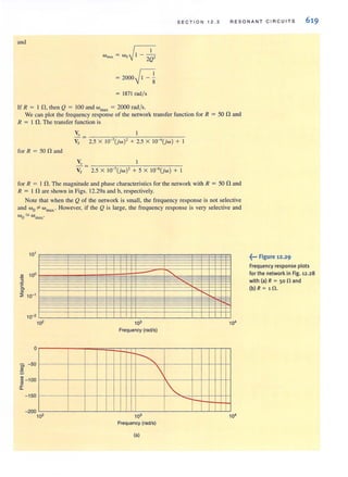
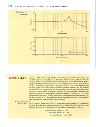
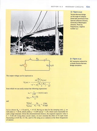
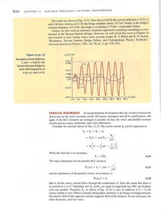
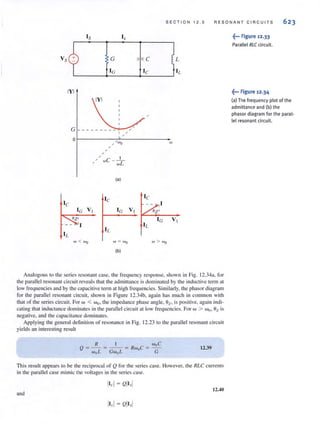
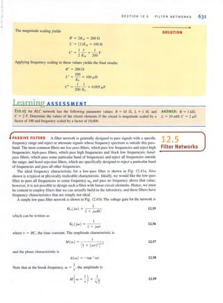
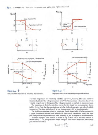
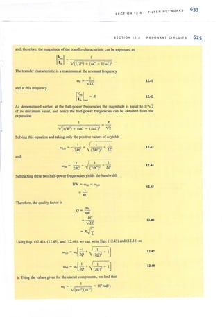
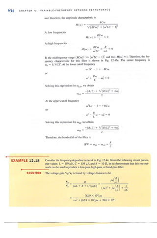
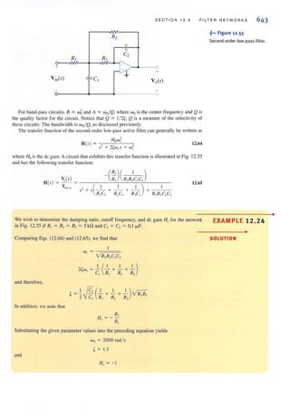
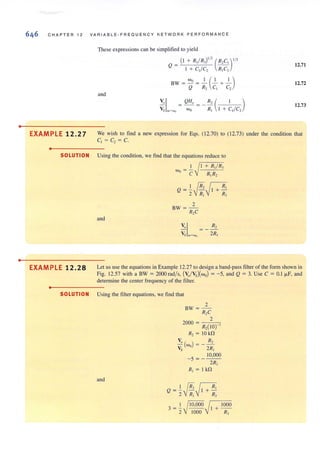
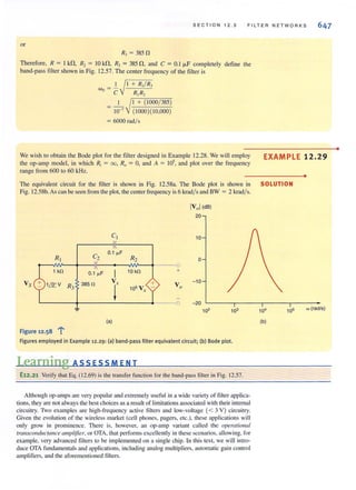
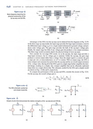
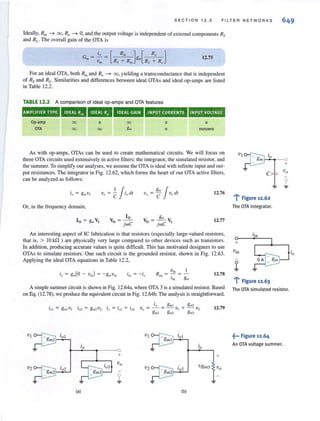
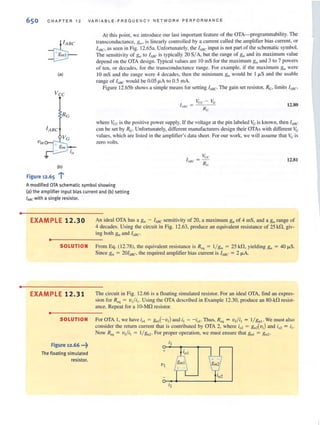
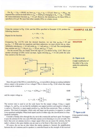
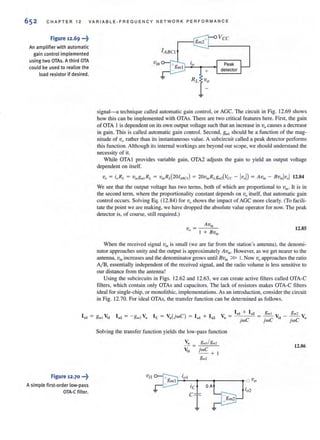
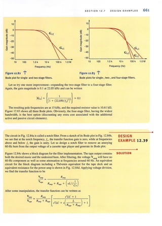
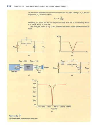
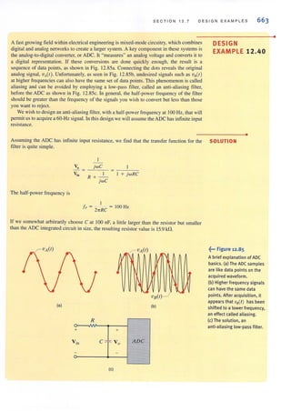
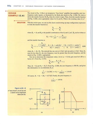
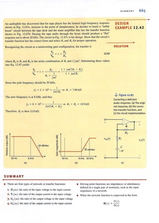
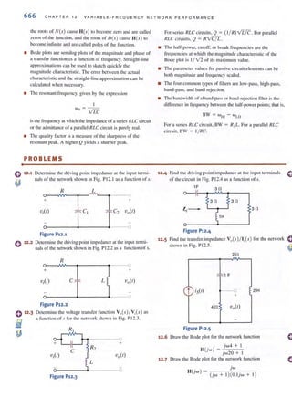
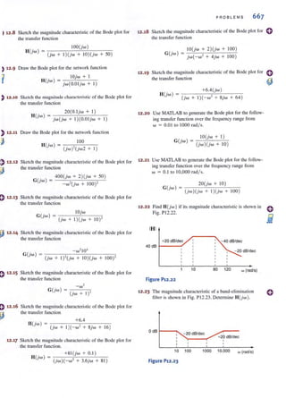
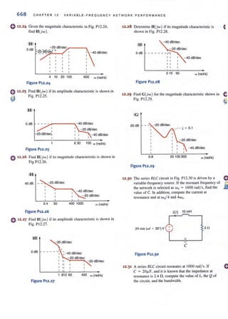
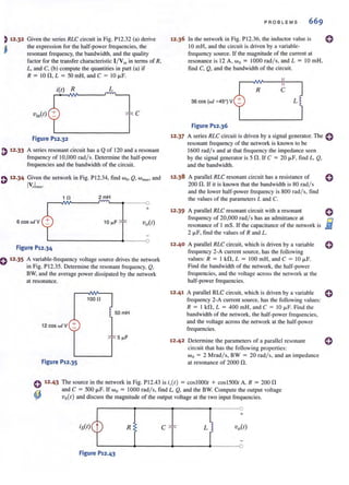
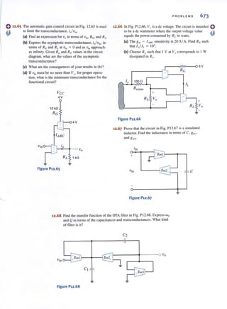

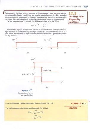
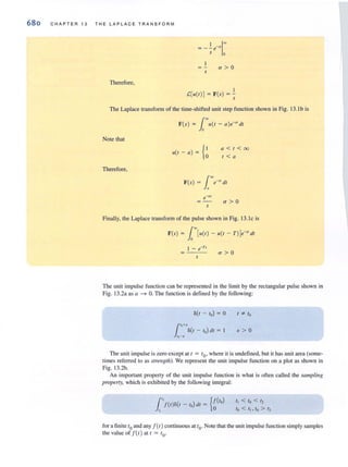
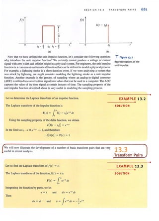
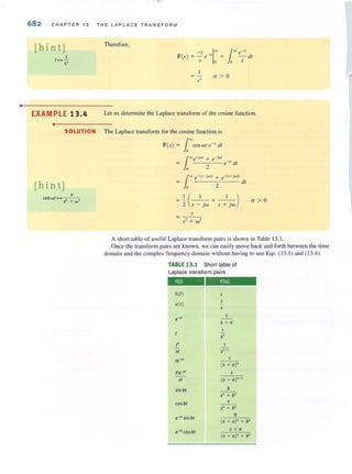
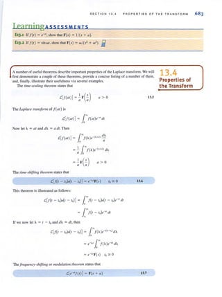
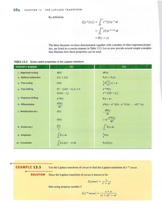
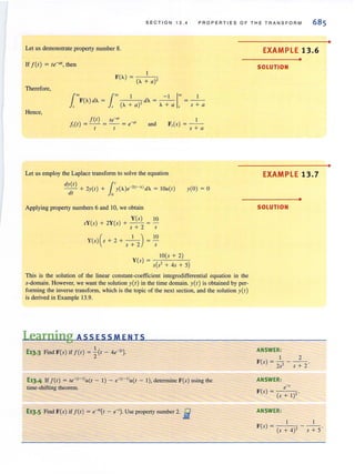
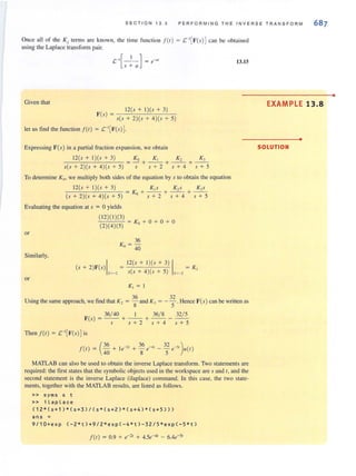
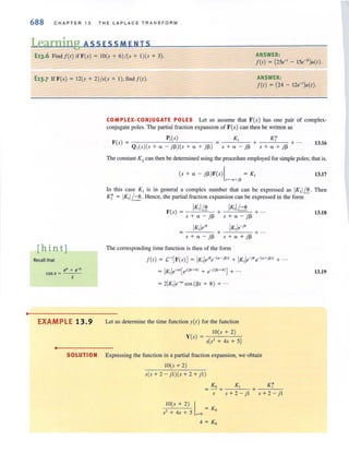
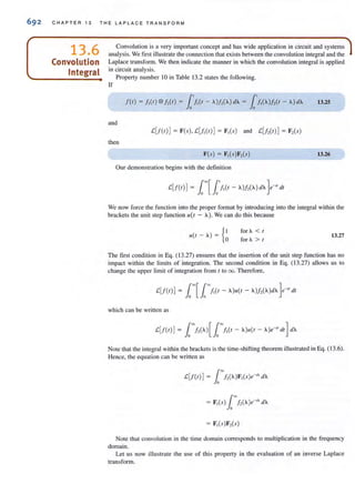
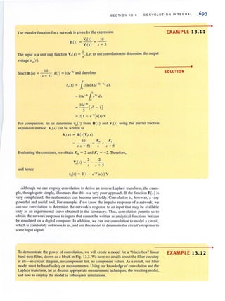
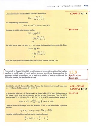
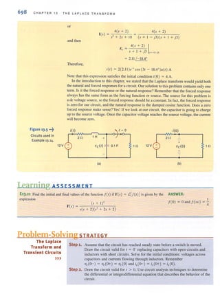
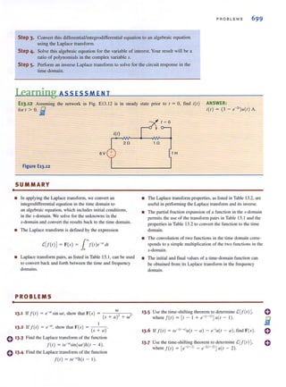
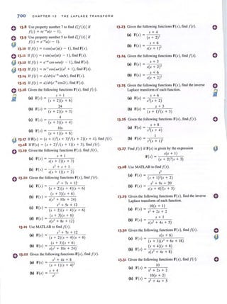
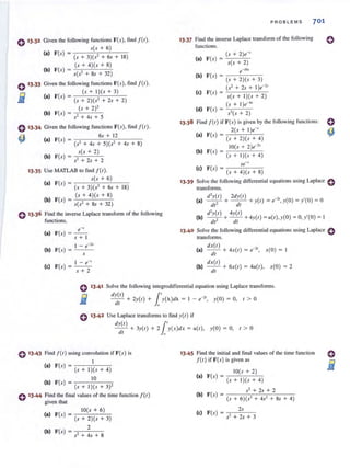
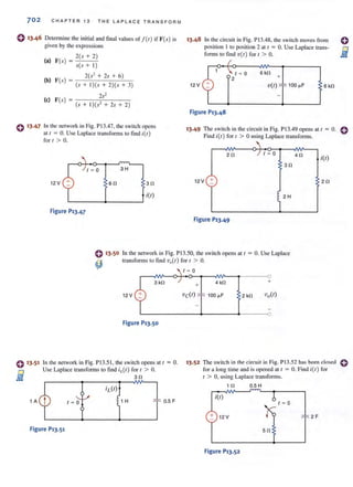
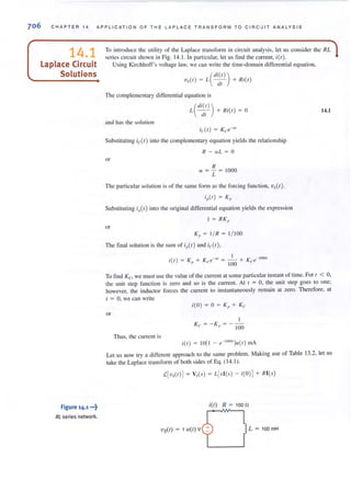
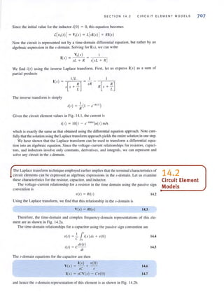
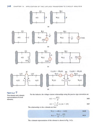
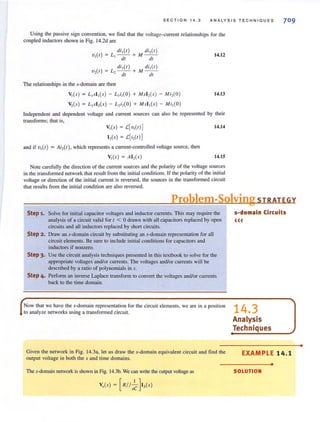
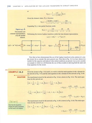
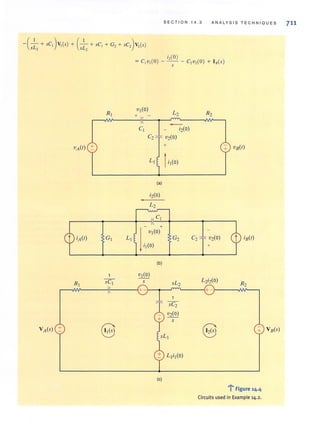
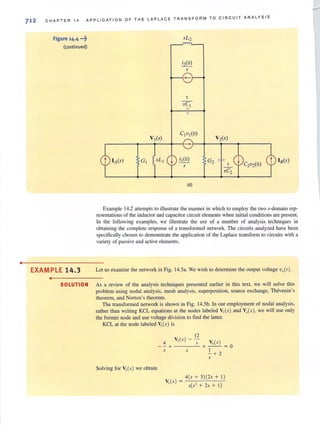
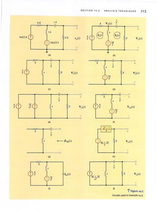
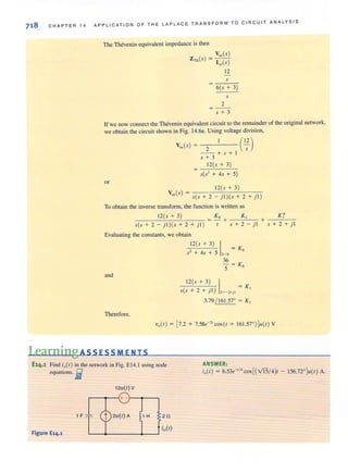
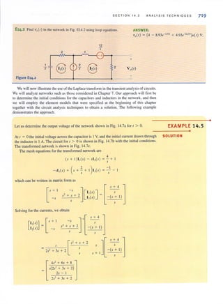
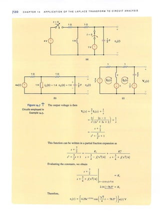
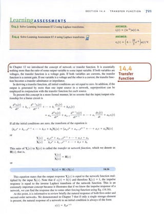
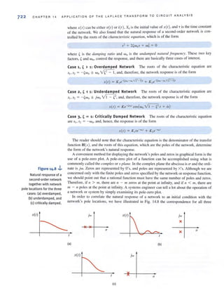
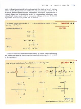
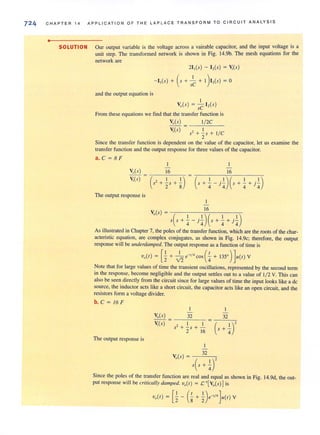
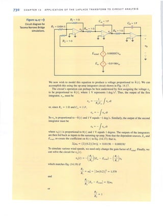
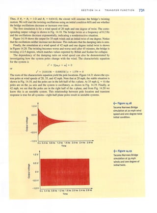
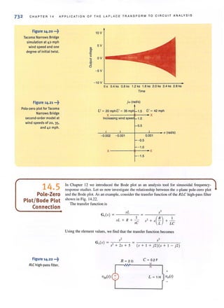
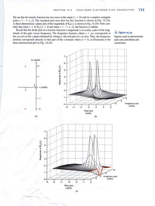
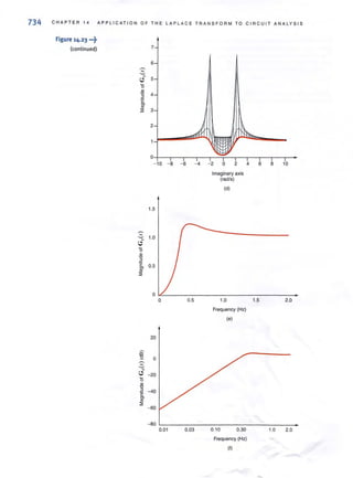
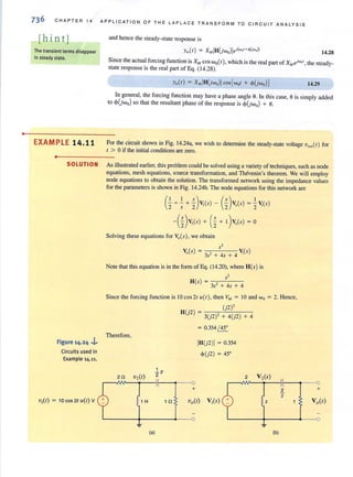
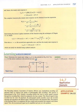
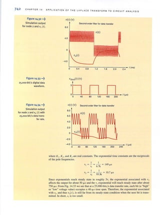
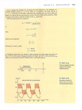
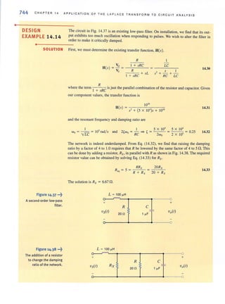
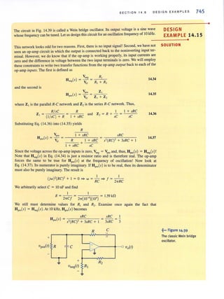
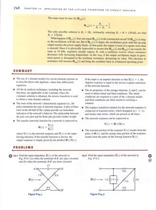

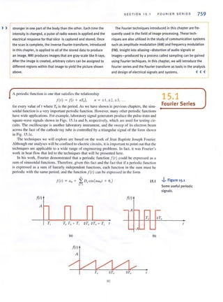
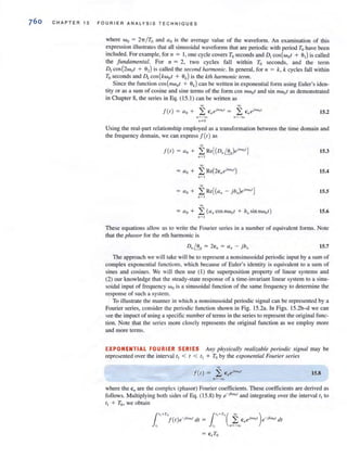
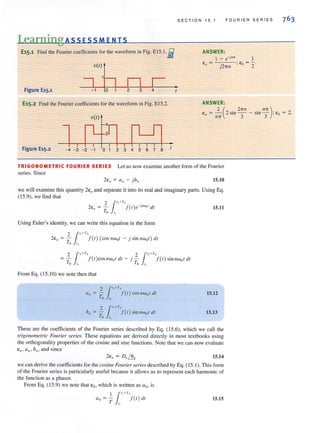
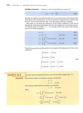
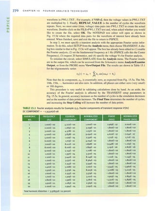
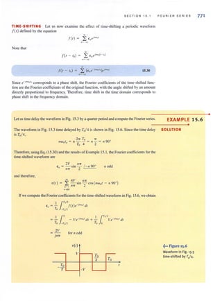
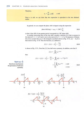
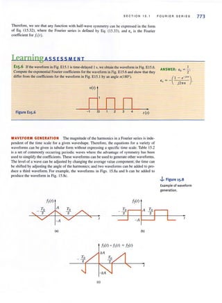
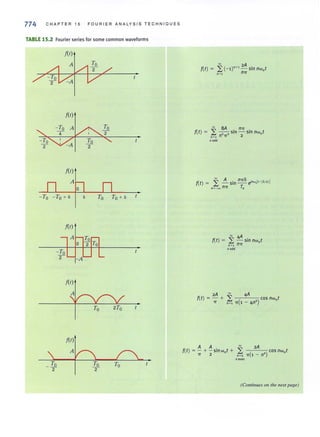
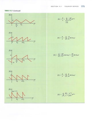
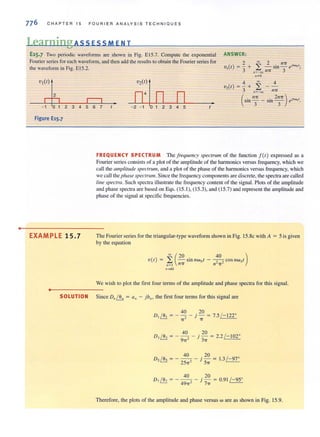
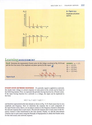
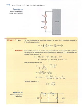
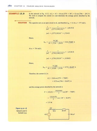
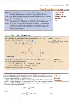
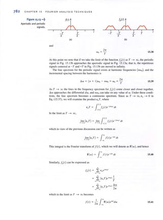
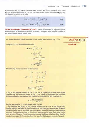
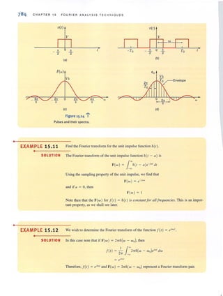
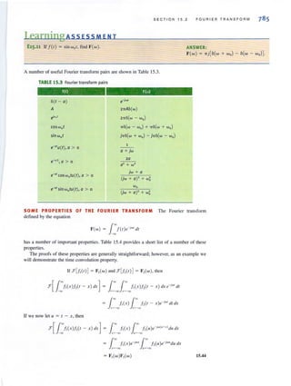
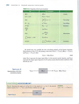
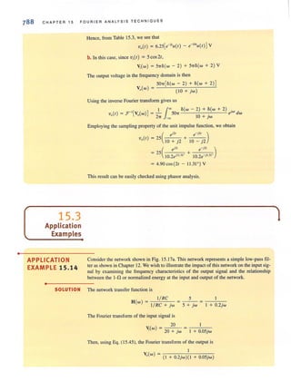
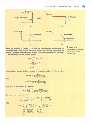
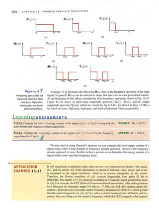
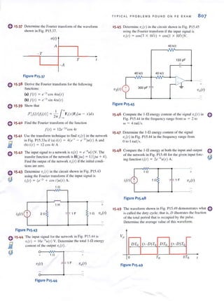
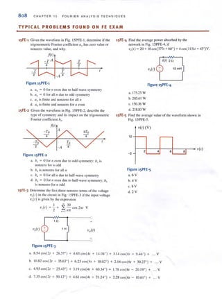

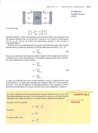
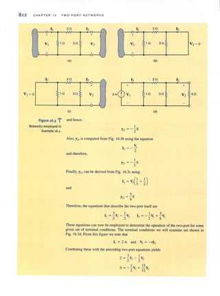
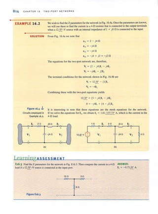
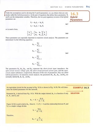
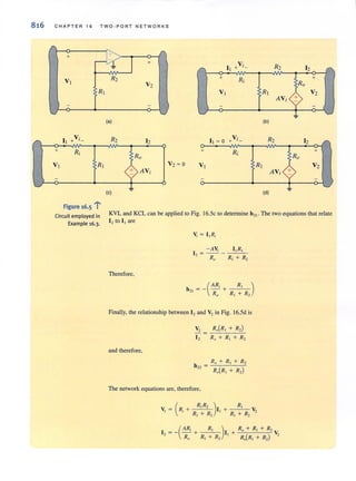
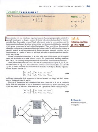
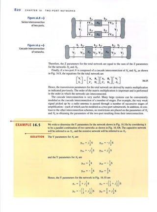
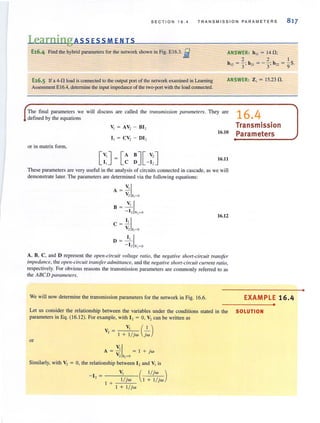
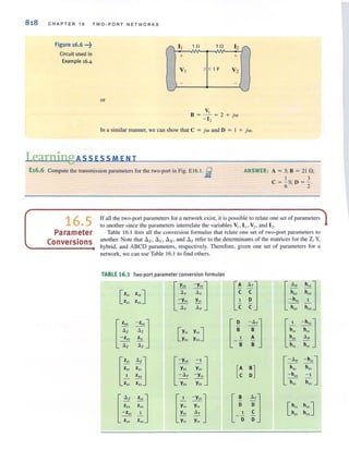
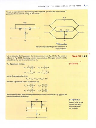
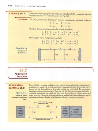
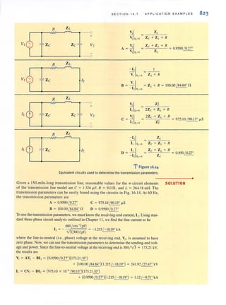
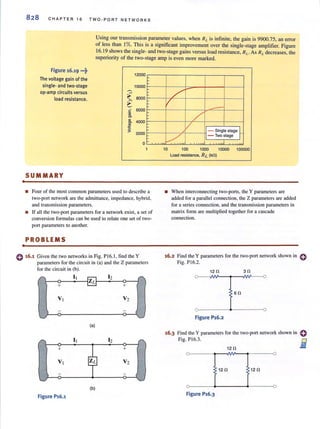
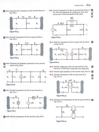
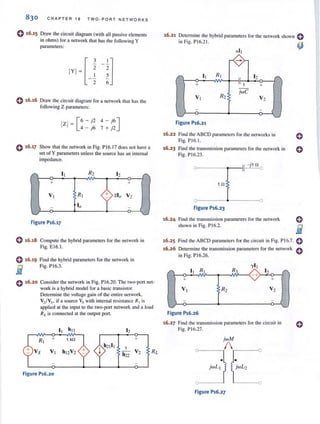
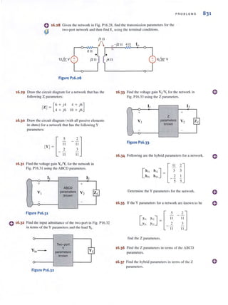

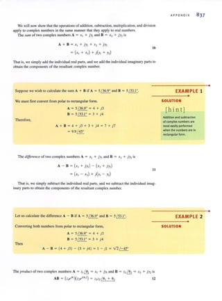
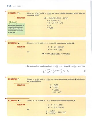
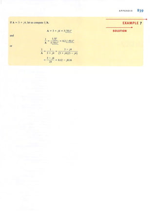


This document provides a list of staff members and credits for a book on basic engineering circuit analysis. It includes the names and roles of the senior acquisitions editor, project editor, senior production editor, executive marketing manager, senior designer, senior illustration editor, senior photo editor, media editor, editorial assistant, interior design, cover design, and photographers. It also provides copyright information and publishing details for the book.