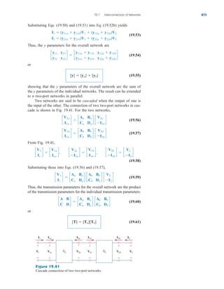
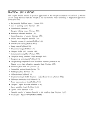
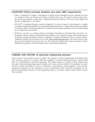
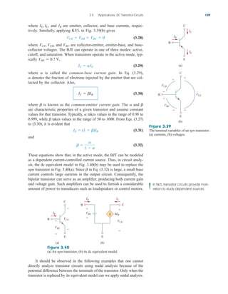
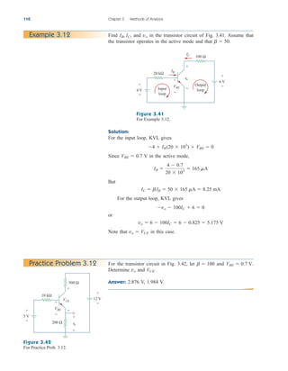
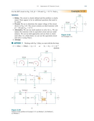
This document provides an overview of the practical applications covered in a textbook on electric circuits. It lists over 30 specific examples of applications, such as designing lighting systems, reading a voltmeter, modeling transducers, and calculating the number of stations allowable in an AM broadcast band. These applications are included to help students apply circuit concepts to real-life situations. The document also discusses computer tools like PSpice and MATLAB that are introduced in the textbook to allow circuit analysis.


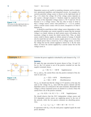


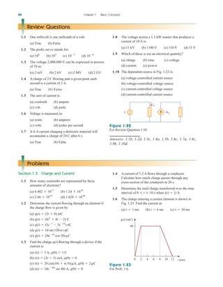


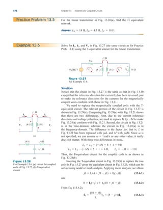
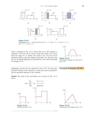
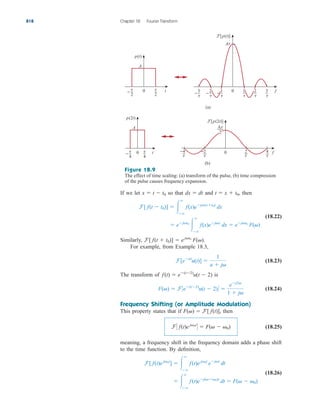
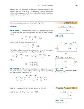
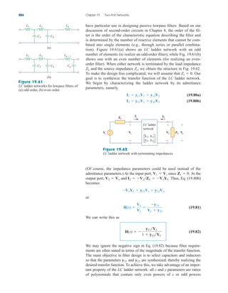
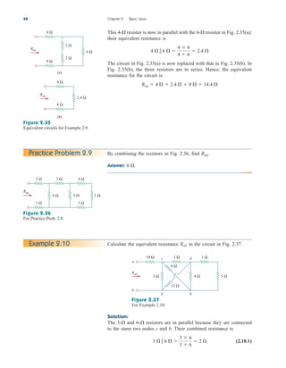
![is short circuited, as shown in Fig. 2.33(a), two things should be kept
in mind:
1. The equivalent resistance [See what happens when
in Eq. (2.37).]
2. The entire current flows through the short circuit.
As another extreme case, suppose that is, is an open
circuit, as shown in Fig. 2.33(b). The current still flows through the
path of least resistance, By taking the limit of Eq. (2.37) as
we obtain in this case.
If we divide both the numerator and denominator by Eq. (2.43)
becomes
(2.44a)
(2.44b)
Thus, in general, if a current divider has N conductors
in parallel with the source current i, the nth conductor ( ) will have
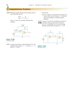
current
(2.45)
In general, it is often convenient and possible to combine resis-
tors in series and parallel and reduce a resistive network to a single
equivalent resistance Such an equivalent resistance is the resist-
ance between the designated terminals of the network and must
exhibit the same i-v characteristics as the original network at the
terminals.
Req.
in
Gn
G1 G2 p GN
i
Gn
(G1, G2, p , GN)
i2
G2
G1 G2
i
i1
G1
G1 G2
i
R1R2,
Req R1
R2 S ,
R1.
R2
R2 ,
R2 0
Req 0.
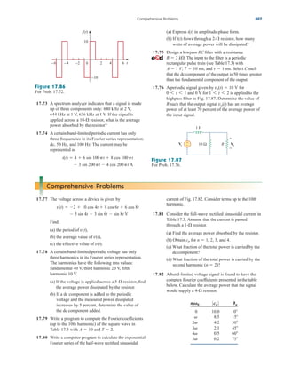
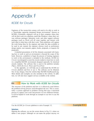
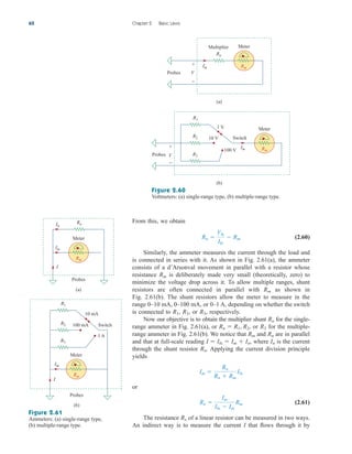
2.6 Parallel Resistors and Current Division 47
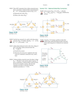
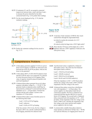
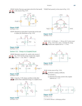
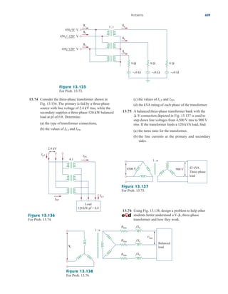
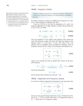
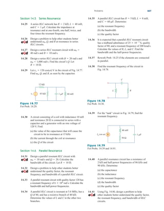
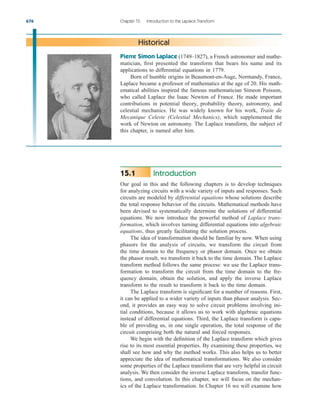
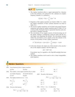
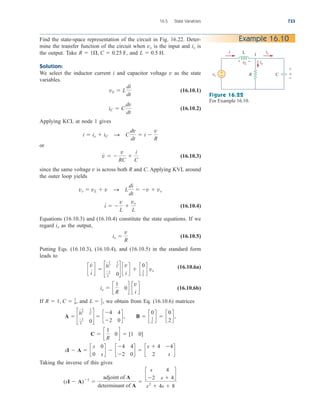
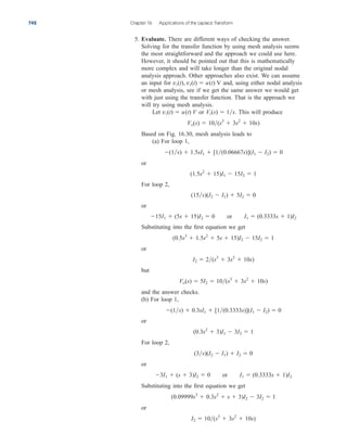
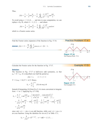
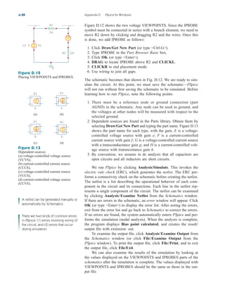
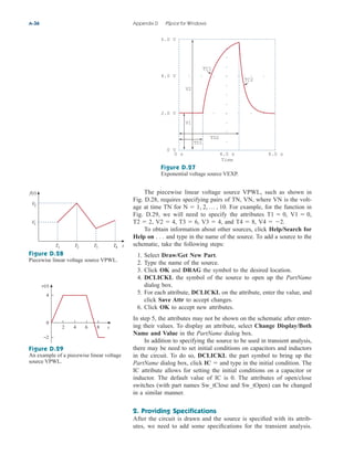
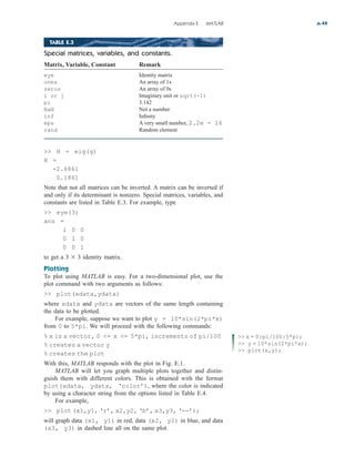
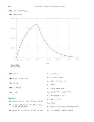
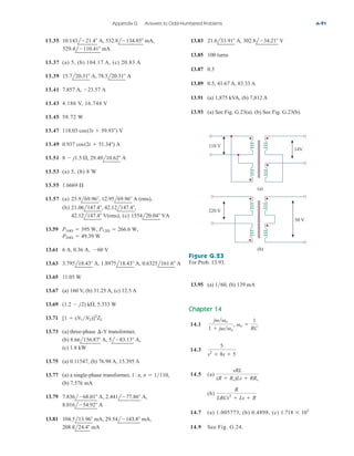
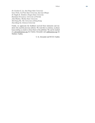
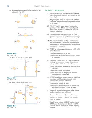
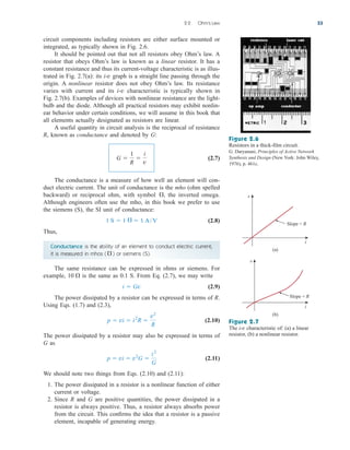
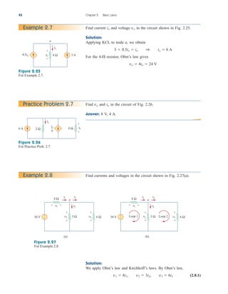
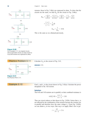
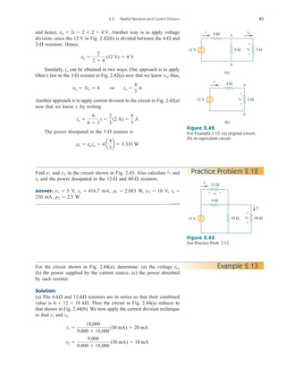
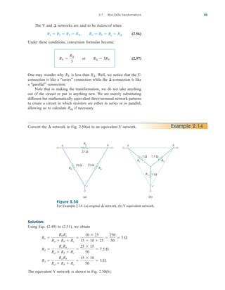
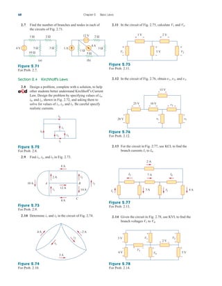
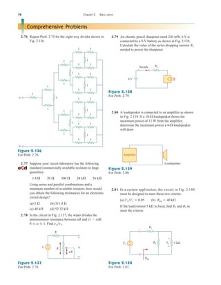
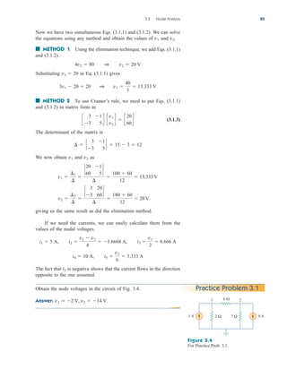
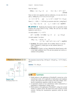
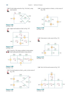
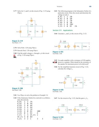
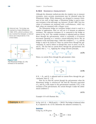
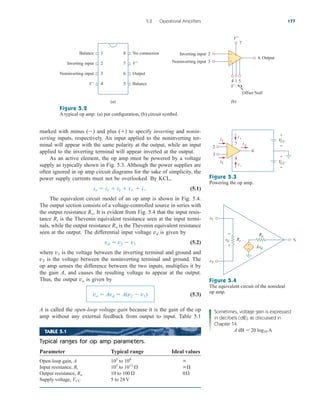
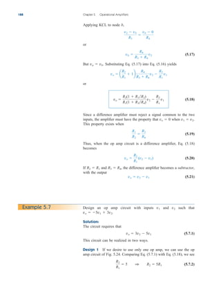
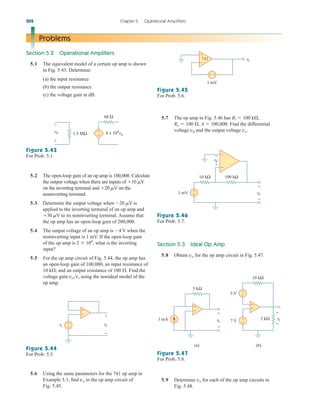
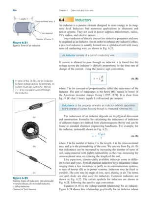
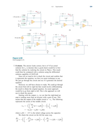
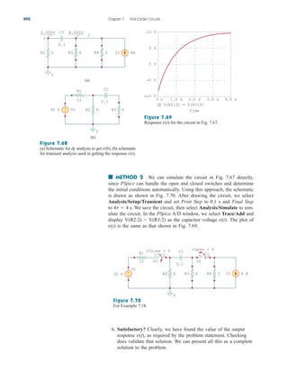
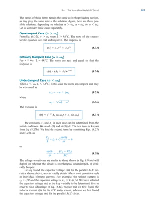
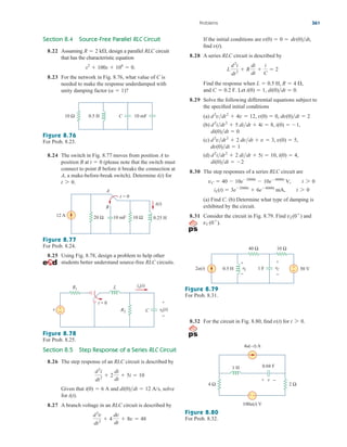
Example 2.9
Figure 2.34
For Example 2.9.
2 Ω
5 Ω
Req
4 Ω
8 Ω
1 Ω
6 Ω 3 Ω
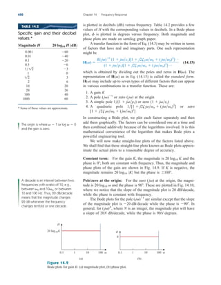
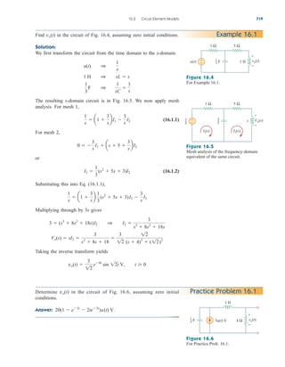
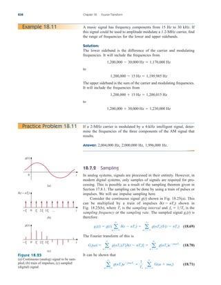
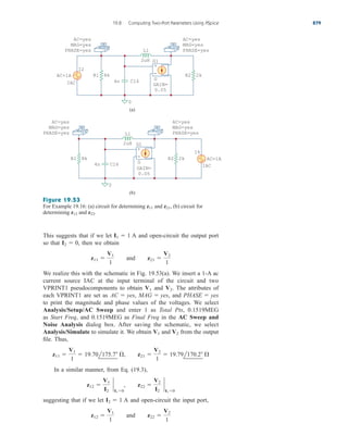
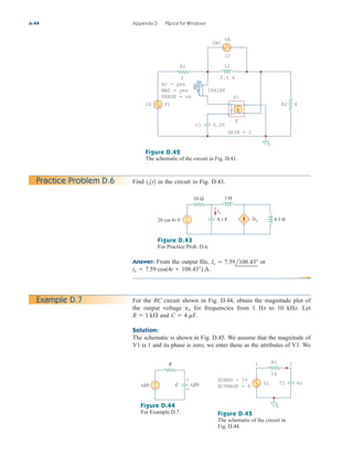
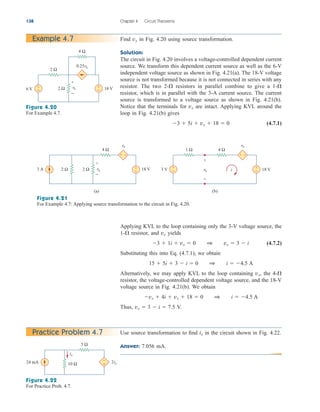
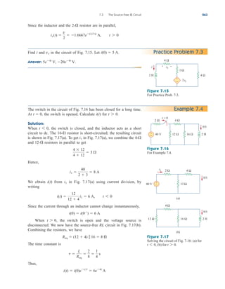
Find for the circuit shown in Fig. 2.34.
Solution:
To get we combine resistors in series and in parallel. The 6- and
3- resistors are in parallel, so their equivalent resistance is
(The symbol is used to indicate a parallel combination.) Also, the 1-
and 5- resistors are in series; hence their equivalent resistance is
Thus the circuit in Fig. 2.34 is reduced to that in Fig. 2.35(a). In
Fig. 2.35(a), we notice that the two 2- resistors are in series, so the
equivalent resistance is
2 2 4
1 5 6
6 3
6 3
6 3
2
Req,
Req
ale29559_ch02.qxd 07/09/2008 11:19 AM Page 47](https://image.slidesharecdn.com/fundamentalsofelectriccircuits4thed-220903233817-99157c39/85/Fundamentals_of_Electric_Circuits_4th_Ed-pdf-79-320.jpg)


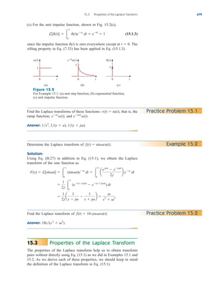
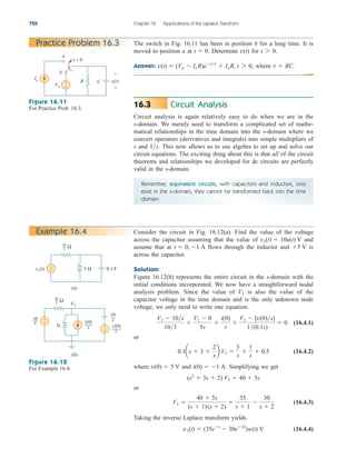
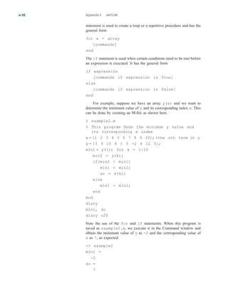
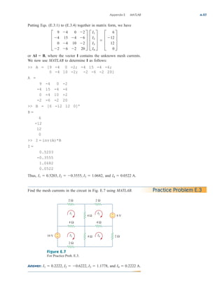
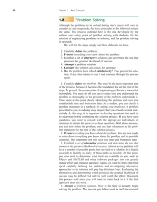
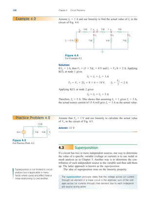
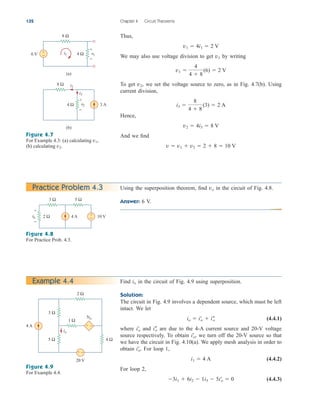
![88 Chapter 3 Methods of Analysis
Thus, we find
as we obtained with Method 1.
■ METHOD 3 We now use MATLAB to solve the matrix. Equa-
tion (3.2.6) can be written as
where A is the 3 by 3 square matrix, B is the column vector, and V is
a column vector comprised of and that we want to determine.
We use MATLAB to determine V as follows:
A [3 2 1; 4 7 1; 2 3 1];
B [12 0 0];
V inv(A) * B
Thus, and as obtained previously.
v3 2.4 V,
v2 2.4 V,
v1 4.8 V,
V
4.8000
2.4000
2.4000
v3
v2,
v1,
AV B 1 V A1
B
v3
¢3
¢
24
10
2.4 V
v1
¢1
¢
48
10
4.8 V, v2
¢2
¢
24
10
2.4 V
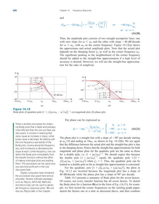
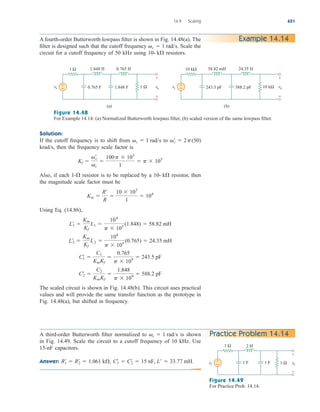
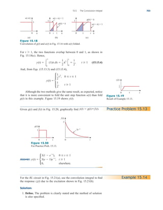
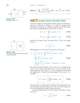
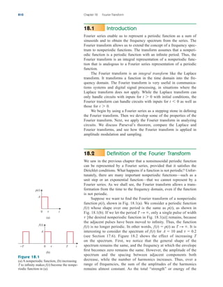
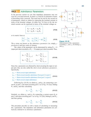
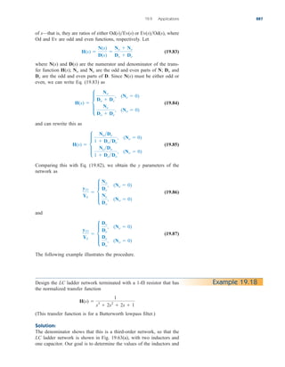
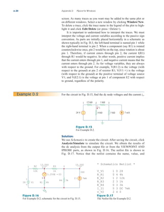
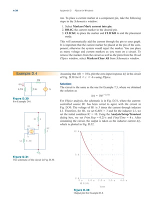
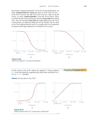
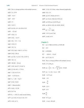
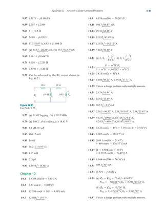
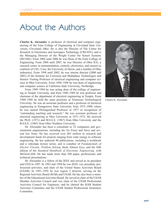
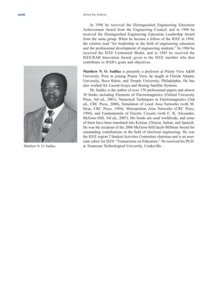
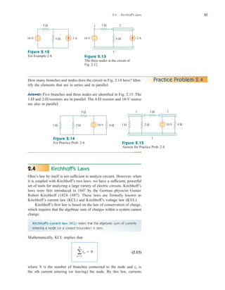
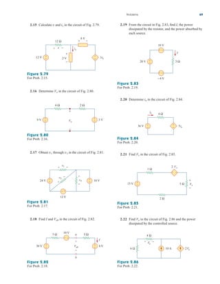
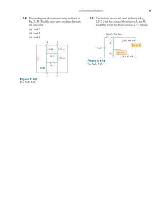
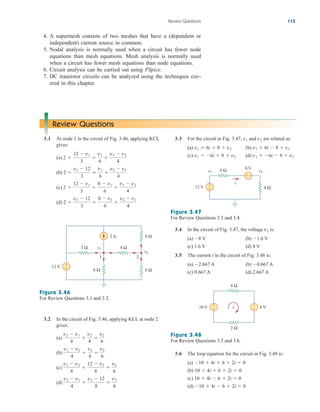
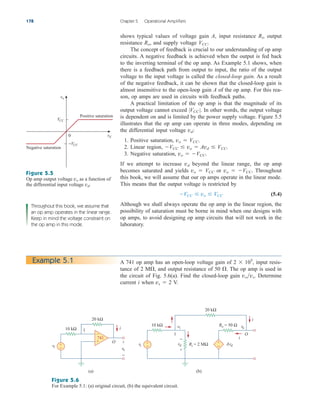
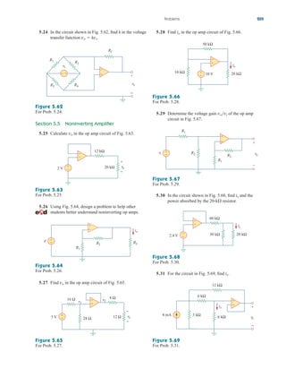
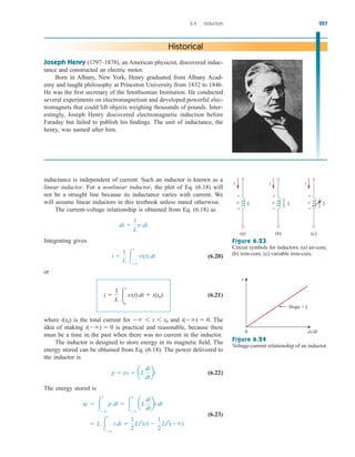
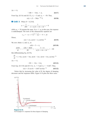
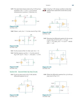
Practice Problem 3.2 Find the voltages at the three nonreference nodes in the circuit of
Fig. 3.6.
Answer: v1 80 V, v2 64 V, v3 156 V.
Figure 3.6
For Practice Prob. 3.2.
10 A
2 Ω
3 Ω
4 Ω 6 Ω
ix
4ix
1 3
2
Nodal Analysis with Voltage Sources
We now consider how voltage sources affect nodal analysis. We use the
circuit in Fig. 3.7 for illustration. Consider the following two possibilities.
■ CASE 1 If a voltage source is connected between the reference
node and a nonreference node, we simply set the voltage at the non-
reference node equal to the voltage of the voltage source. In Fig. 3.7,
for example,
(3.10)
Thus, our analysis is somewhat simplified by this knowledge of the volt-
age at this node.
■ CASE 2 If the voltage source (dependent or independent) is con-
nected between two nonreference nodes, the two nonreference nodes
v1 10 V
3.3
ale29559_ch03.qxd 07/08/2008 10:46 AM Page 88](https://image.slidesharecdn.com/fundamentalsofelectriccircuits4thed-220903233817-99157c39/85/Fundamentals_of_Electric_Circuits_4th_Ed-pdf-120-320.jpg)


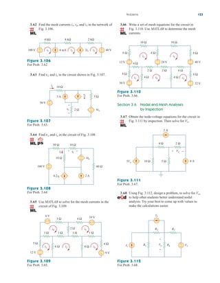


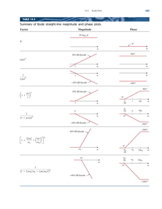
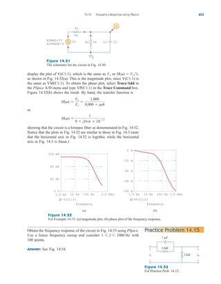
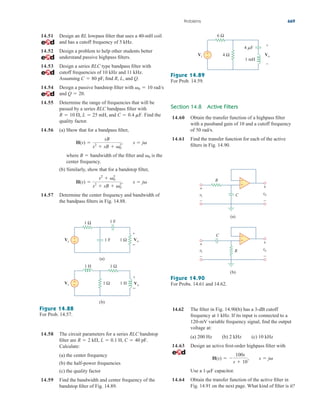
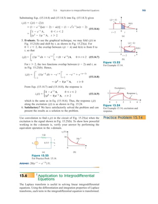
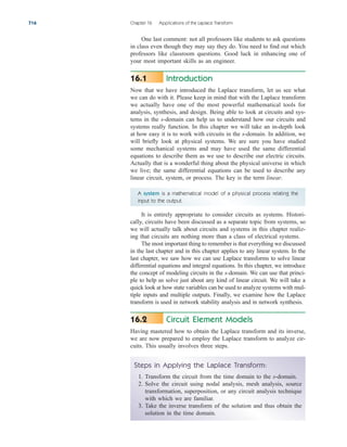
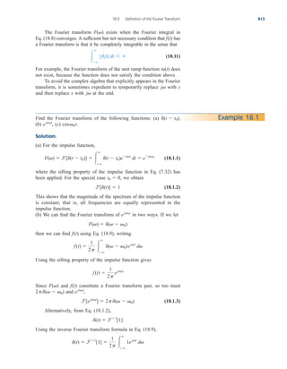
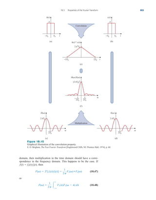
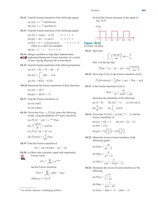
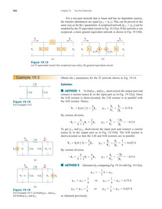
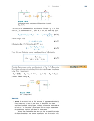
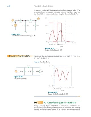
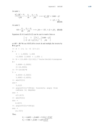
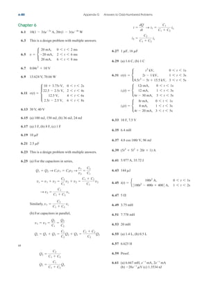
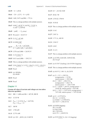
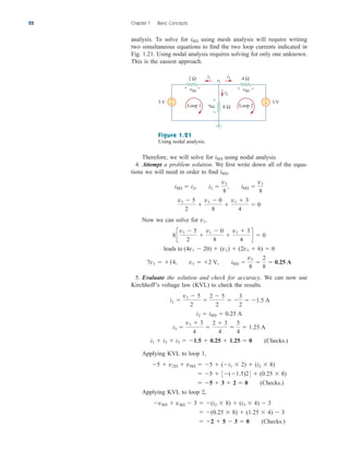
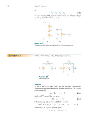
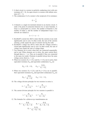
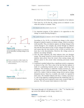
![The value 2k in item 7 is necessary for a bias point calculation; it
cannot be left blank.
The third step is to set up the DC Sweep to sweep the parameter.
To do this:
1. Select Analysis/Setput to bring up the DC Sweep dialog box.
2. For the Sweep Type, select Linear (or Octave for a wide range
of ).
3. For the Sweep Var. Type, select Global Parameter.
4. Under the Name box, enter RL.
5. In the Start Value box, enter 100.
6. In the End Value box, enter 5k.
7. In the Increment box, enter 100.
8. Click OK and Close to accept the parameters.
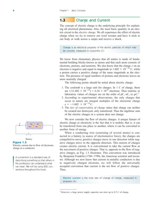
After taking these steps and saving the circuit, we are ready to
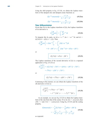
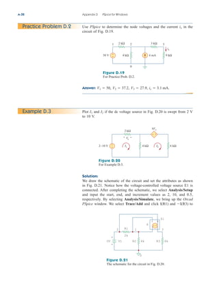
simulate. Select Analysis/Simulate. If there are no errors, we select
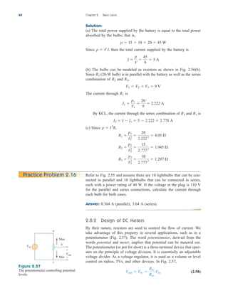
Add Trace in the PSpice window and type in
the Trace Command box. [The negative sign is needed since I(R2) is
negative.] This gives the plot of the power delivered to as varies
from to . We can also obtain the power absorbed by by
typing in the Trace Command box. Either way,
we obtain the plot in Fig. 4.57. It is evident from the plot that the
maximum power is Notice that the maximum occurs when
as expected analytically.
RL 1 k,
250 mW.
V(R2:2)*V(R2:2)/RL
RL
5 k
100
RL
RL
V(R2:2)*I(R2)
A/D
RL
4.10 Applications 155
250 uW
150 uW
200 uW
100 uW
50 uW
0 2.0 K 4.0 K 6.0 K
–V(R2:2)*I(R2)
RL
Figure 4.57
For Example 4.15: the plot of power
across RL.
Practice Problem 4.15
Find the maximum power transferred to if the resistor in
Fig. 4.55 is replaced by a resistor.
Answer: 125 mW.
2-k
1-k
RL
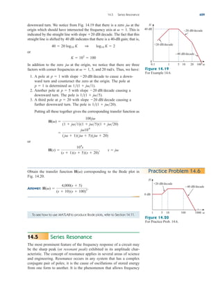
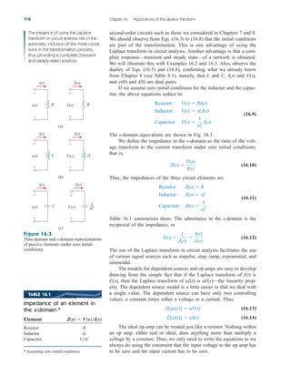
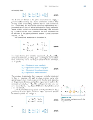
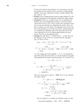
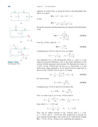
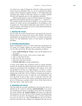
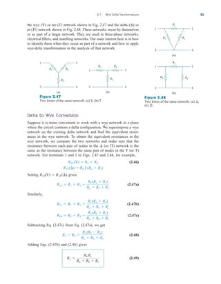
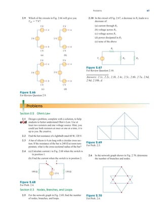
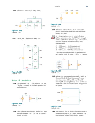
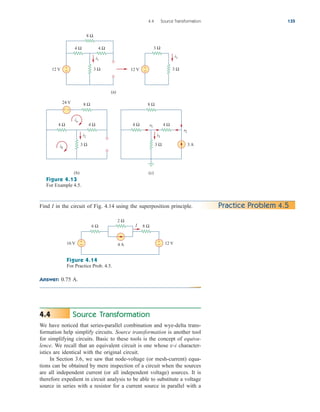
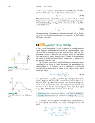
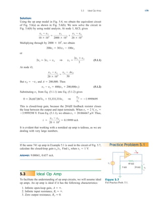
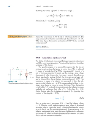
Applications
In this section we will discuss two important practical applications of
the concepts covered in this chapter: source modeling and resistance
measurement.
4.10.1 Source Modeling
Source modeling provides an example of the usefulness of the
Thevenin or the Norton equivalent. An active source such as a battery
is often characterized by its Thevenin or Norton equivalent circuit. An
ideal voltage source provides a constant voltage irrespective of the cur-
rent drawn by the load, while an ideal current source supplies a con-
stant current regardless of the load voltage. As Fig. 4.58 shows,
practical voltage and current sources are not ideal, due to their inter-
nal resistances or source resistances and They become ideal as
To show that this is the case, consider the effect
Rs S 0 and Rp S .
Rp.
Rs
4.10
vs
Rs
+
−
(a)
is
Rp
(b)
Figure 4.58
(a) Practical voltage source, (b) practical
current source.
ale29559_ch04.qxd 07/08/2008 10:56 AM Page 155](https://image.slidesharecdn.com/fundamentalsofelectriccircuits4thed-220903233817-99157c39/85/Fundamentals_of_Electric_Circuits_4th_Ed-pdf-187-320.jpg)


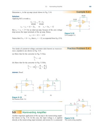


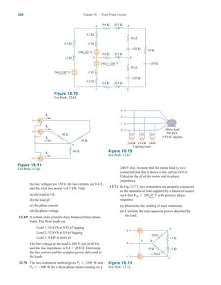
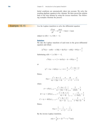
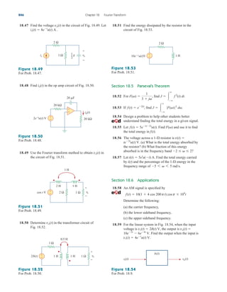
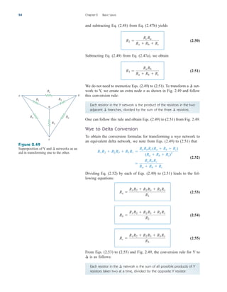
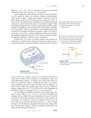
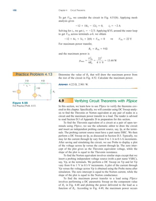
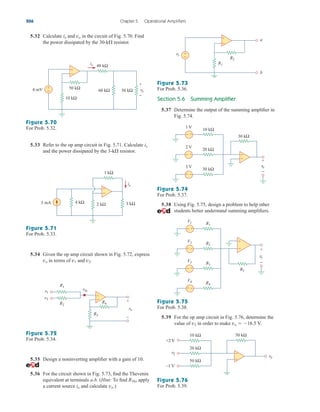
![Applications
The op amp is a fundamental building block in modern electronic
instrumentation. It is used extensively in many devices, along with
resistors and other passive elements. Its numerous practical applications
include instrumentation amplifiers, digital-to-analog converters, analog
computers, level shifters, filters, calibration circuits, inverters, sum-
mers, integrators, differentiators, subtractors, logarithmic amplifiers,
comparators, gyrators, oscillators, rectifiers, regulators, voltage-to-
current converters, current-to-voltage converters, and clippers. Some of
these we have already considered. We will consider two more applica-
tions here: the digital-to-analog converter and the instrumentation
amplifier.
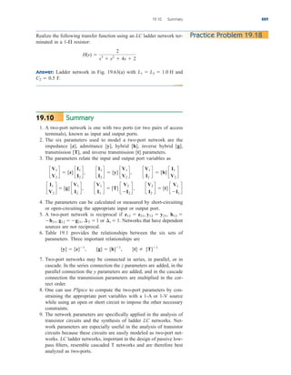
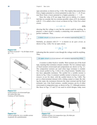
5.10.1 Digital-to-Analog Converter
The digital-to-analog converter (DAC) transforms digital signals into
analog form. A typical example of a four-bit DAC is illustrated in
Fig. 5.36(a). The four-bit DAC can be realized in many ways. A sim-
ple realization is the binary weighted ladder, shown in Fig. 5.36(b).
The bits are weights according to the magnitude of their place value,
by descending value of RfRn so that each lesser bit has half the
weight of the next higher. This is obviously an inverting summing
amplifier. The output is related to the inputs as shown in Eq. (5.15).
Thus,
(5.23)
Input V1 is called the most significant bit (MSB), while input V4 is the
least significant bit (LSB). Each of the four binary inputs V1, ... , V4
can assume only two voltage levels: 0 or 1 V. By using the proper input
and feedback resistor values, the DAC provides a single output that is
proportional to the inputs.
Vo
Rf
R1
V1
Rf
R2
V2
Rf
R3
V3
Rf
R4
V4
5.10
196 Chapter 5 Operational Amplifiers
In practice, the voltage levels may be
typically 0 and ; 5 V.
Analog
output
Digital
input
(0000–1111)
Four-bit
DAC
(a)
+
−
V1 V2 V3 V4
R1 R2 R3 R4
Rf
V
o
MSB LSB
(b)
Figure 5.36
Four-bit DAC: (a) block diagram, (b)
binary weighted ladder type.
Example 5.12 In the op amp circuit of Fig. 5.36(b), let Rf 10 k, R1 10 k,
R2 20 k, R3 40 k, and R4 80 k. Obtain the analog output
for binary inputs [0000], [0001], [0010],..., [1111].
Solution:
Substituting the given values of the input and feedback resistors in
Eq. (5.23) gives
Using this equation, a digital input [V1V2V3V4] [0000] produces an ana-
log output of Vo 0 V; [V1V2V3V4] [0001] gives Vo 0.125 V.
V1 0.5V2 0.25V3 0.125V4
Vo
Rf
R1
V1
Rf
R2
V2
Rf
R3
V3
Rf
R4
V4
ale29559_ch05.qxd 07/16/2008 05:19 PM Page 196](https://image.slidesharecdn.com/fundamentalsofelectriccircuits4thed-220903233817-99157c39/85/Fundamentals_of_Electric_Circuits_4th_Ed-pdf-228-320.jpg)
![Similarly,
Table 5.2 summarizes the result of the digital-to-analog conversion.
Note that we have assumed that each bit has a value of 0.125 V. Thus,
in this system, we cannot represent a voltage between 1.000 and 1.125,
for example. This lack of resolution is a major limitation of digital-to-
analog conversions. For greater accuracy, a word representation with a
greater number of bits is required. Even then a digital representation
of an analog voltage is never exact. In spite of this inexact represen-
tation, digital representation has been used to accomplish remarkable
things such as audio CDs and digital photography.
1.875 V
3V1 V2 V3 V4 4 311114 1 Vo 1 0.5 0.25 0.125
o
3V1 V2 V3 V4 4 301004 1 Vo 0.5 V
3V1 V2 V3 V4 4 300114 1 Vo 0.25 0.125 0.375 V
3V1 V2 V3 V4 4 300104 1 Vo 0.25 V
5.10 Applications 197
TABLE 5.2
Input and output values of the four-bit DAC.
Binary input Output
[V1V2V3V4] Decimal value Vo
0000 0 0
0001 1 0.125
0010 2 0.25
0011 3 0.375
0100 4 0.5
0101 5 0.625
0110 6 0.75
0111 7 0.875
1000 8 1.0
1001 9 1.125
1010 10 1.25
1011 11 1.375
1100 12 1.5
1101 13 1.625
1110 14 1.75
1111 15 1.875
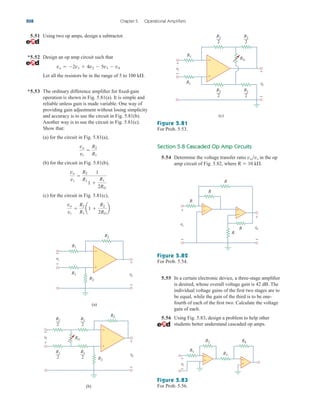
Practice Problem 5.12
A three-bit DAC is shown in Fig. 5.37.
(a) Determine |Vo| for [V1V2V3] [010].
(b) Find |Vo| if [V1V2V3] [110].
(c) If |Vo| 1.25 V is desired, what should be [V1V2V3]?
(d) To get |Vo| 1.75 V, what should be [V1V2V3]?
Answer: 0.5 V, 1.5 V, [101], [111].
Figure 5.37
Three-bit DAC; for Practice Prob. 5.12.
+
−
10 kΩ
20 kΩ
40 kΩ
10 kΩ
v1
v2
v3
vo
ale29559_ch05.qxd 07/16/2008 05:19 PM Page 197](https://image.slidesharecdn.com/fundamentalsofelectriccircuits4thed-220903233817-99157c39/85/Fundamentals_of_Electric_Circuits_4th_Ed-pdf-229-320.jpg)


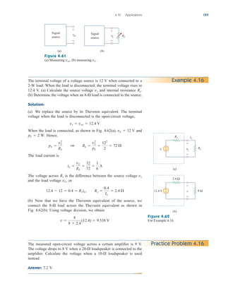
![5.80 Use PSpice to solve Prob. 5.70.
5.81 Use PSpice to verify the results in Example 5.9.
Assume nonideal op amps LM324.
Section 5.10 Applications
5.82 A five-bit DAC covers a voltage range of 0 to 7.75 V.
Calculate how much voltage each bit is worth.
5.83 Design a six-bit digital-to-analog converter.
(a) If |Vo| 1.1875 V is desired, what should
[V1V2V3V4V5V6] be?
(b) Calculate |Vo| if [V1V2V3V4V5V6] [011011].
(c) What is the maximum value |Vo| can assume?
*5.84 A four-bit R-2R ladder DAC is presented in Fig. 5.103.
(a) Show that the output voltage is given by
(b) If Rf 12 k and R 10 k, find |Vo| for
[V1V2V3V4] [1011] and [V1V2V3V4] [0101].
Vo Rf a
V1
2R
V2
4R
V3
8R
V4
16R
b
5.86 Design a voltage controlled ideal current source
(within the operating limits of the op amp) where the
output current is equal to .
5.87 Figure 5.105 displays a two-op-amp instrumentation
amplifier. Derive an expression for vo in terms of v1
and v2. How can this amplifier be used as a
subtractor?
200 vs(t) mA.
212 Chapter 5 Operational Amplifiers
R
R
R
R
V
o
+
−
V1
V2
V3
V4
2R
2R
2R
2R
Rf
Figure 5.103
For Prob. 5.84.
Figure 5.105
For Prob. 5.87.
Figure 5.106
For Prob. 5.88.
Figure 5.104
For Prob. 5.85.
5.85 In the op amp circuit of Fig. 5.104, find the value of
R so that the power absorbed by the 10-k resistor is
10 mW. Take vs 2 V.
R
vs
+
−
−
+
40 kΩ
10 kΩ
v2
v1
vo
R4
R3
R2
R1
+
−
+
−
*5.88 Figure 5.106 shows an instrumentation amplifier
driven by a bridge. Obtain the gain vovi of the
amplifier.
25 kΩ
10 kΩ
10 kΩ
500 kΩ
vo
25 kΩ
2 kΩ
30 kΩ
20 kΩ
vi
80 kΩ
40 kΩ
500 kΩ
+
−
+
−
+
−
ale29559_ch05.qxd 07/16/2008 05:20 PM Page 212](https://image.slidesharecdn.com/fundamentalsofelectriccircuits4thed-220903233817-99157c39/85/Fundamentals_of_Electric_Circuits_4th_Ed-pdf-244-320.jpg)


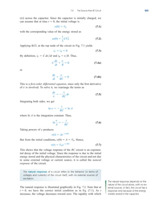
![For the switch is opened, and we have the RC circuit
shown in Fig. 7.9(b). [Notice that the RC circuit in Fig. 7.9(b) is
source free; the independent source in Fig. 7.8 is needed to provide
or the initial energy in the capacitor.] The and resistors
in series give
The time constant is
Thus, the voltage across the capacitor for is
or
The initial energy stored in the capacitor is
wC (0)
1
2
Cv2
C (0)
1
2
20 103
152
2.25 J
v(t) 15e5t
V
v(t) vC (0)ett
15et0.2
V
t 0
t ReqC 10 20 103
0.2 s
Req 1 9 10
9-
1-
V0
t 7 0,
7.3 The Source-Free RL Circuit 259
Figure 7.9
For Example 7.2: (a) (b) t 7 0.
t 6 0,
If the switch in Fig. 7.10 opens at find for and
Answer: 5.33 J.
8e2t
V,
wC (0).
t 0
v(t)
t 0, Practice Problem 7.2
Figure 7.10
For Practice Prob. 7.2.
The Source-Free RL Circuit
Consider the series connection of a resistor and an inductor, as shown
in Fig. 7.11. Our goal is to determine the circuit response, which we
will assume to be the current through the inductor. We select the
inductor current as the response in order to take advantage of the idea
that the inductor current cannot change instantaneously. At we
assume that the inductor has an initial current or
(7.13)
with the corresponding energy stored in the inductor as
(7.14)
Applying KVL around the loop in Fig. 7.11,
(7.15)
But and Thus,
L
di
dt
Ri 0
vR iR.
vL L didt
vL vR 0
w(0)
1
2
L I2
0
i(0) I0
I0,
t 0,
i(t)
7.3
Figure 7.11
A source-free RL circuit.
9 Ω
1 Ω
vC(0)
3 Ω
+
−
+
−
20 V
(a)
9 Ω
1 Ω
(b)
+
−
Vo = 15 V 20 mF
6 Ω
+
−
24 V
+
−
v 12 Ω 4 Ω
t = 0
F
1
6
vL
+
−
R
L
i
vR
+
−
ale29559_ch07.qxd 07/08/2008 11:49 AM Page 259](https://image.slidesharecdn.com/fundamentalsofelectriccircuits4thed-220903233817-99157c39/85/Fundamentals_of_Electric_Circuits_4th_Ed-pdf-291-320.jpg)


![The unit step function u(t) is 0 for negative values of t and 1 for pos-
itive values of t.
The three most widely used singularity functions in circuit analy-
sis are the unit step, the unit impulse, and the unit ramp functions.
266 Chapter 7 First-Order Circuits
In mathematical terms,
(7.24)
The unit step function is undefined at where it changes abruptly
from 0 to 1. It is dimensionless, like other mathematical functions such
as sine and cosine. Figure 7.23 depicts the unit step function. If the
abrupt change occurs at (where ) instead of the unit
step function becomes
(7.25)
which is the same as saying that is delayed by seconds, as shown
in Fig. 7.24(a). To get Eq. (7.25) from Eq. (7.24), we simply replace
every t by If the change is at the unit step function
becomes
(7.26)
meaning that is advanced by seconds, as shown in Fig. 7.24(b).
We use the step function to represent an abrupt change in voltage
or current, like the changes that occur in the circuits of control systems
and digital computers. For example, the voltage
(7.27)
may be expressed in terms of the unit step function as
(7.28)
If we let then is simply the step voltage A voltage
source of is shown in Fig. 7.25(a); its equivalent circuit is shown
in Fig. 7.25(b). It is evident in Fig. 7.25(b) that terminals a-b are short-
circuited ( ) for and that appears at the terminals
v V0
t 6 0
v 0
V0 u(t)
V0 u(t).
v(t)
t0 0,
v(t) V0u(t t0)
v(t) b
0, t 6 t0
V0, t 7 t0
t0
u(t)
u(t t0) b
0, t 6 t0
1, t 7 t0
t t0,
t t0.
t0
u(t)
u(t t0) b
0, t 6 t0
1, t 7 t0
t 0,
t0 7 0
t t0
t 0,
u(t) b
0, t 6 0
1, t 7 0
Figure 7.25
(a) Voltage source of (b) its equivalent circuit.
V0u(t),
Figure 7.23
The unit step function.
Figure 7.24
(a) The unit step function delayed by
(b) the unit step advanced by t0.
t0,
Alternatively, we may derive
Eqs. (7.25) and (7.26) from Eq. (7.24)
by writing u[f(t)] 1, f(t) 0,
where f(t) may be t t0 or t t0.
7
0 t
1
u(t)
0 t
1
u(t − t0)
t0
(a)
0 t
u(t + t0)
−t0
(b)
1
+
−
(a)
V0u(t) +
−
(b)
V0
b
a
b
a
t = 0
=
ale29559_ch07.qxd 07/08/2008 11:49 AM Page 266](https://image.slidesharecdn.com/fundamentalsofelectriccircuits4thed-220903233817-99157c39/85/Fundamentals_of_Electric_Circuits_4th_Ed-pdf-298-320.jpg)


![or by integration as
(7.39)
Although there are many more singularity functions, we are only inter-
ested in these three (the impulse function, the unit step function, and
the ramp function) at this point.
u(t)
t
d(t)dt, r(t)
t
u(t)dt
7.4 Singularity Functions 269
Express the voltage pulse in Fig. 7.31 in terms of the unit step. Cal-
culate its derivative and sketch it.
Solution:
The type of pulse in Fig. 7.31 is called the gate function. It may be
regarded as a step function that switches on at one value of t and
switches off at another value of t. The gate function shown in Fig. 7.31
switches on at and switches off at It consists of the
sum of two unit step functions as shown in Fig. 7.32(a). From the
figure, it is evident that
Taking the derivative of this gives
which is shown in Fig. 7.32(b). We can obtain Fig. 7.32(b) directly
from Fig. 7.31 by simply observing that there is a sudden increase by
10 V at leading to At there is a sudden
decrease by 10 V leading to 10 V d(t 5).
t 5 s,
10d(t 2).
t 2 s
dv
dt
10[d(t 2) d(t 5)]
v(t) 10u(t 2) 10u(t 5) 10[u(t 2) u(t 5)]
t 5 s.
t 2 s
Example 7.6
Gate functions are used along
with switches to pass or block
another signal.
Figure 7.31
For Example 7.6.
Figure 7.32
(a) Decomposition of the pulse in Fig. 7.31, (b) derivative of the pulse in Fig. 7.31.
0 t
10
v(t)
3 4 5
1 2
0 t
2
1
10
10u(t − 2) −10u(t − 5)
(a)
1 2
0
3 4 5 t
10
−10
+
(b)
10
3 4 5 t
1 2
0
−10
dv
dt
ale29559_ch07.qxd 07/08/2008 11:49 AM Page 269](https://image.slidesharecdn.com/fundamentalsofelectriccircuits4thed-220903233817-99157c39/85/Fundamentals_of_Electric_Circuits_4th_Ed-pdf-301-320.jpg)
![270 Chapter 7 First-Order Circuits
Express the current pulse in Fig. 7.33 in terms of the unit step. Find
its integral and sketch it.
Answer:
See Fig. 7.34.
r(t 4)].
10[u(t) 2u(t 2) u(t 4)], 10[r(t) 2r(t 2)
Practice Problem 7.6
Figure 7.33
For Practice Prob. 7.6.
Figure 7.34
Integral of in Fig. 7.33.
i(t)
Express the sawtooth function shown in Fig. 7.35 in terms of singu-
larity functions.
Solution:
There are three ways of solving this problem. The first method is by
mere observation of the given function, while the other methods
involve some graphical manipulations of the function.
■ METHOD 1 By looking at the sketch of in Fig. 7.35, it is
not hard to notice that the given function is a combination of sin-
gularity functions. So we let
(7.7.1)
The function is the ramp function of slope 5, shown in Fig. 7.36(a);
that is,
(7.7.2)
v1(t) 5r(t)
v1(t)
v(t) v1(t) v2(t) p
v(t)
v(t)
Example 7.7
Figure 7.35
For Example 7.7.
Figure 7.36
Partial decomposition of in Fig. 7.35.
v(t)
0
t
10
−10
i(t)
2 4
2
0 4 t
20
i dt
∫
0 t
10
v(t)
2
0 t
10
v1(t)
2 0 t
10
v1 + v2
2
0
t
−10
v2(t)
2
+
(a) (b) (c)
=
ale29559_ch07.qxd 07/08/2008 11:49 AM Page 270](https://image.slidesharecdn.com/fundamentalsofelectriccircuits4thed-220903233817-99157c39/85/Fundamentals_of_Electric_Circuits_4th_Ed-pdf-302-320.jpg)
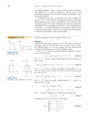
![Since goes to infinity, we need another function at in order to
get We let this function be which is a ramp function of slope
as shown in Fig. 7.36(b); that is,
(7.7.3)
Adding and gives us the signal in Fig. 7.36(c). Obviously, this is
not the same as in Fig. 7.35. But the difference is simply a constant
10 units for By adding a third signal where
(7.7.4)
we get as shown in Fig. 7.37. Substituting Eqs. (7.7.2) through
(7.7.4) into Eq. (7.7.1) gives
v(t) 5r(t) 5r(t 2) 10u(t 2)
v(t),
v3 10u(t 2)
v3,
t 7 2 s.
v(t)
v2
v1
v2(t) 5r(t 2)
5,
v2,
v(t).
t 2 s
v1(t)
7.4 Singularity Functions 271
Figure 7.37
Complete decomposition of in Fig. 7.35.
v(t)
■ METHOD 2 A close observation of Fig. 7.35 reveals that is
a multiplication of two functions: a ramp function and a gate function.
Thus,
the same as before.
■ METHOD 3 This method is similar to Method 2. We observe
from Fig. 7.35 that is a multiplication of a ramp function and a
unit step function, as shown in Fig. 7.38. Thus,
If we replace by then we can replace by
Hence,
which can be simplified as in Method 2 to get the same result.
v(t) 5r(t)[1 u(t 2)]
1 u(t 2).
u(t 2)
1 u(t),
u(t)
v(t) 5r(t)u(t 2)
v(t)
5r(t) 5r(t 2) 10u(t 2)
5r(t) 5(t 2)u(t 2) 10u(t 2)
5r(t) 5(t 2 2)u(t 2)
5tu(t) 5tu(t 2)
v(t) 5t[u(t) u(t 2)]
v(t)
0 t
10
v1 + v2
2
+
(c)
(a)
=
0 t
10
v(t)
2
0
t
−10
v3(t)
2
(b)
ale29559_ch07.qxd 07/08/2008 11:49 AM Page 271](https://image.slidesharecdn.com/fundamentalsofelectriccircuits4thed-220903233817-99157c39/85/Fundamentals_of_Electric_Circuits_4th_Ed-pdf-303-320.jpg)
![272 Chapter 7 First-Order Circuits
Refer to Fig. 7.39. Express in terms of singularity functions.
Answer: 2u(t) 2r(t) 4r(t 2) 2r(t 3).
i(t)
Practice Problem 7.7
Figure 7.38
Decomposition of in Fig. 7.35.
v(t)
Figure 7.39
For Practice Prob. 7.7.
Given the signal
express in terms of step and ramp functions.
Solution:
The signal may be regarded as the sum of three functions specified
within the three intervals and
For may be regarded as 3 multiplied by where
for and 0 for Within the time interval
the function may be considered as multiplied by a
gated function For the function may be
regarded as multiplied by the unit step function Thus,
One may avoid the trouble of using by replacing it with
Then
Alternatively, we may plot and apply Method 1 from Example 7.7.
g(t)
g(t) 3[1 u(t)] 2u(t) 2r(t 1) 3 5u(t) 2r(t 1)
1 u(t).
u(t)
3u(t) 2u(t) 2r(t 1)
3u(t) 2u(t) 2(t 1)u(t 1)
3u(t) 2u(t) (2t 4 2)u(t 1)
g(t) 3u(t) 2[u(t) u(t 1)] (2t 4)u(t 1)
u(t 1).
2t 4
t 7 1,
[u(t) u(t 1)].
2
0 6 t 6 1,
t 7 0.
t 6 0
u(t) 1
u(t),
t 6 0, g(t)
t 7 1.
t 6 0, 0 6 t 6 1,
g(t)
g(t)
g(t) c
3, t 6 0
2, 0 6 t 6 1
2t 4, t 7 1
Example 7.8
0 t
10
5r(t)
2
×
0 t
u(−t + 2)
2
1
i(t) (A)
1
0
2 3 t (s)
2
−2
ale29559_ch07.qxd 07/08/2008 11:49 AM Page 272](https://image.slidesharecdn.com/fundamentalsofelectriccircuits4thed-220903233817-99157c39/85/Fundamentals_of_Electric_Circuits_4th_Ed-pdf-304-320.jpg)
![7.5 Step Response of an RC Circuit 273
If
express in terms of the singularity functions.
Answer: 8u(t) 2u(t 2) 2r(t 2) 18u(t 6) 2r(t 6).
h(t)
h(t) d
0, t 6 0
8, 0 6 t 6 2
2t 6, 2 6 t 6 6
0, t 7 6
Practice Problem 7.8
Example 7.9
Evaluate the following integrals involving the impulse function:
Solution:
For the first integral, we apply the sifting property in Eq. (7.32).
Similarly, for the second integral,
e1
cos 1 e1
sin (1) 0.1988 2.2873 2.0885
et
cos t 0t1 et
sin t0t1
[d(t 1)et
cos t d(t 1)et
sin t]dt
10
0
(t2
4t 2)d(t 2)dt (t2
4t 2)0t2 4 8 2 10
[d(t 1)et
cos t d(t 1)et
sin t]dt
10
0
(t2
4t 2)d(t 2)dt
Evaluate the following integrals:
Answer: 28, 1.
(t3
5t2
10)d(t 3)dt,
10
0
d(t p) cos 3t dt
Practice Problem 7.9
Step Response of an RC Circuit
When the dc source of an RC circuit is suddenly applied, the voltage
or current source can be modeled as a step function, and the response
is known as a step response.
7.5
The step response of a circuit is its behavior when the excitation is the
step function, which may be a voltage or a current source.
ale29559_ch07.qxd 07/08/2008 11:49 AM Page 273](https://image.slidesharecdn.com/fundamentalsofelectriccircuits4thed-220903233817-99157c39/85/Fundamentals_of_Electric_Circuits_4th_Ed-pdf-305-320.jpg)


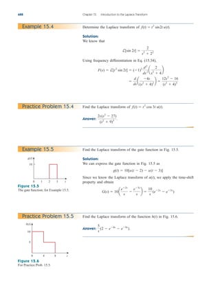
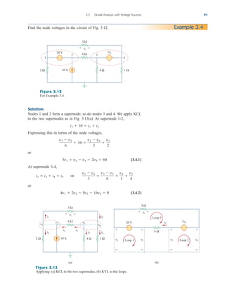
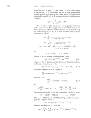
![Another way of looking at the complete response is to break into
two components—one temporary and the other permanent, i.e.,
or
(7.51)
where
(7.52a)
and
(7.52b)
The transient response is temporary; it is the portion of the com-
plete response that decays to zero as time approaches infinity. Thus,
vt
vss Vs
vt (Vo Vs)ett
v vt vss
Complete response transient response
temporary part
steady-state response
permanent part
276 Chapter 7 First-Order Circuits
The transient response is the circuit’s temporary response that will die
out with time.
The steady-state response is the portion of the complete response
that remains after the transient reponse has died out. Thus,
vss
The first decomposition of the complete response is in terms of the
source of the responses, while the second decomposition is in terms of
the permanency of the responses. Under certain conditions, the natural
response and transient response are the same. The same can be said
about the forced response and steady-state response.
Whichever way we look at it, the complete response in Eq. (7.45)
may be written as
(7.53)
where is the initial voltage at and is the final or steady-
state value. Thus, to find the step response of an RC circuit requires
three things:
v()
t 0
v(0)
v(t) v() [v(0) v()]ett
The steady-state response is the behavior of the circuit a long time
after an external excitation is applied.
1. The initial capacitor voltage
2. The final capacitor voltage
3. The time constant t.
v().
v(0).
We obtain item 1 from the given circuit for and items 2 and 3
from the circuit for Once these items are determined, we obtain
t 7 0.
t 6 0
This is the same as saying that the com-
plete response is the sum of the tran-
sient response and the steady-state
response.
Once we know x(0), x( ), and ,
almost all the circuit problems in this
chapter can be solved using the
formula
x(t) x() 3x(0) x()4ett
t
ale29559_ch07.qxd 07/08/2008 11:49 AM Page 276](https://image.slidesharecdn.com/fundamentalsofelectriccircuits4thed-220903233817-99157c39/85/Fundamentals_of_Electric_Circuits_4th_Ed-pdf-308-320.jpg)
![the response using Eq. (7.53). This technique equally applies to RL cir-
cuits, as we shall see in the next section.
Note that if the switch changes position at time instead of
at there is a time delay in the response so that Eq. (7.53)
becomes
(7.54)
where is the initial value at Keep in mind that Eq. (7.53)
or (7.54) applies only to step responses, that is, when the input exci-
tation is constant.
t t0
.
v(t0)
v(t) v() [v(t0) v()]e(tt0)t
t 0,
t t0
7.5 Step Response of an RC Circuit 277
The switch in Fig. 7.43 has been in position A for a long time. At
the switch moves to B. Determine for and calculate its value
at and 4 s.
t 1 s
t 7 0
v(t)
t 0, Example 7.10
Figure 7.43
For Example 7.10.
Solution:
For the switch is at position A. The capacitor acts like an open
circuit to dc, but v is the same as the voltage across the resistor.
Hence, the voltage across the capacitor just before is obtained
by voltage division as
Using the fact that the capacitor voltage cannot change instantaneously,
For the switch is in position B. The Thevenin resistance
connected to the capacitor is and the time constant is
Since the capacitor acts like an open circuit to dc at steady state,
Thus,
At
At
v(4) 30 15e2
27.97 V
t 4,
v(1) 30 15e0.5
20.9 V
t 1,
30 (15 30)et2
(30 15e0.5t
) V
v(t) v() [v(0) v()]ett
v() 30 V.
t RThC 4 103
0.5 103
2 s
RTh 4 k,
t 7 0,
v(0) v(0
) v(0
) 15 V
v(0
)
5
5 3
(24) 15 V
t 0
5-k
t 6 0,
3 kΩ
24 V 30 V
v
5 kΩ 0.5 mF
4 kΩ
+
−
+
−
t = 0
A B
+
−
ale29559_ch07.qxd 07/08/2008 11:49 AM Page 277](https://image.slidesharecdn.com/fundamentalsofelectriccircuits4thed-220903233817-99157c39/85/Fundamentals_of_Electric_Circuits_4th_Ed-pdf-309-320.jpg)

![The Thevenin resistance at the capacitor terminals is
and the time constant is
Thus,
To obtain i, we notice from Fig. 7.46(b) that i is the sum of the currents
through the resistor and the capacitor; that is,
Notice from Fig. 7.46(b) that is satisfied, as expected.
Hence,
Notice that the capacitor voltage is continuous while the resistor current
is not.
i b
1 A, t 6 0
(1 e0.6t
) A, t 7 0
v b
10 V, t 6 0
(20 10e0.6t
) V, t 0
v 10i 30
1 0.5e0.6t
0.25(0.6)(10)e0.6t
(1 e0.6t
) A
i
v
20
C
dv
dt
20-
20 (10 20)e(35)t
(20 10e0.6t
) V
v(t) v() [v(0) v()]ett
t RTh C
20
3
1
4
5
3
s
RTh 10 20
10 20
30
20
3
7.5 Step Response of an RC Circuit 279
Practice Problem 7.11
The switch in Fig. 7.47 is closed at Find and for all time.
Note that for and 0 for Also, u(t) 1 u(t).
t 7 0.
t 6 0
u(t) 1
v(t)
i(t)
t 0.
Figure 7.47
For Practice Prob. 7.11.
Answer:
v b
20 V, t 6 0
10(1 e1.5t
) V, t 7 0
i(t) b
0, t 6 0
2(1 e1.5t
) A, t 7 0
,
5 Ω
+
−
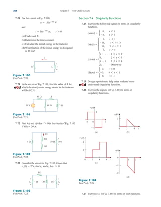
20u(−t) V 10 Ω
0.2 F 3 A
v
i t = 0
+
−
ale29559_ch07.qxd 07/08/2008 11:49 AM Page 279](https://image.slidesharecdn.com/fundamentalsofelectriccircuits4thed-220903233817-99157c39/85/Fundamentals_of_Electric_Circuits_4th_Ed-pdf-311-320.jpg)
![Step Response of an RL Circuit
Consider the RL circuit in Fig. 7.48(a), which may be replaced by the
circuit in Fig. 7.48(b). Again, our goal is to find the inductor current i
as the circuit response. Rather than apply Kirchhoff’s laws, we will use
the simple technique in Eqs. (7.50) through (7.53). Let the response be
the sum of the transient response and the steady-state response,
(7.55)
We know that the transient response is always a decaying exponential,
that is,
(7.56)
where A is a constant to be determined.
The steady-state response is the value of the current a long time after
the switch in Fig. 7.48(a) is closed. We know that the transient response
essentially dies out after five time constants. At that time, the inductor
becomes a short circuit, and the voltage across it is zero. The entire
source voltage appears across R. Thus, the steady-state response is
(7.57)
Substituting Eqs. (7.56) and (7.57) into Eq. (7.55) gives
(7.58)
We now determine the constant A from the initial value of i. Let be
the initial current through the inductor, which may come from a source
other than Since the current through the inductor cannot change
instantaneously,
(7.59)
Thus, at Eq. (7.58) becomes
From this, we obtain A as
Substituting for A in Eq. (7.58), we get
(7.60)
This is the complete response of the RL circuit. It is illustrated in
Fig. 7.49. The response in Eq. (7.60) may be written as
(7.61)
i(t) i() [i(0) i()]ett
i(t)
Vs
R
aI0
Vs
R
bett
A I0
Vs
R
I0 A
Vs
R
t 0,
i(0
) i(0
) I0
Vs.
I0
i Aett
Vs
R
iss
Vs
R
Vs
it Aett
, t
L
R
i it iss
7.6
280 Chapter 7 First-Order Circuits
Figure 7.48
An RL circuit with a step input voltage.
Figure 7.49
Total response of the RL circuit with
initial inductor current I0.
R
Vs
t = 0
i
+
−
+
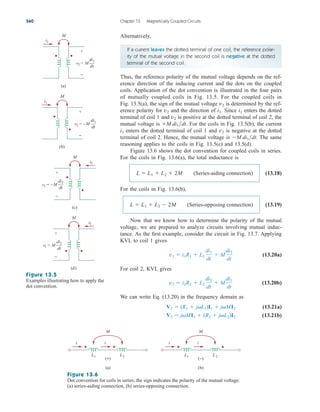
−
v(t)
L
(a)
i
R
Vsu(t) +
−
+
−
v(t)
L
(b)
0 t
i(t)
Vs
R
I0
ale29559_ch07.qxd 07/08/2008 11:49 AM Page 280](https://image.slidesharecdn.com/fundamentalsofelectriccircuits4thed-220903233817-99157c39/85/Fundamentals_of_Electric_Circuits_4th_Ed-pdf-312-320.jpg)
![where and are the initial and final values of i, respectively.
Thus, to find the step response of an RL circuit requires three things:
i()
i(0)
7.6 Step Response of an RL Circuit 281
1. The initial inductor current at
2. The final inductor current
3. The time constant t.
i().
t 0.
i(0)
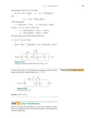
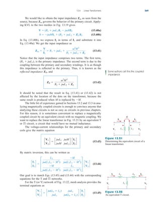
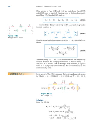
We obtain item 1 from the given circuit for and items 2 and 3
from the circuit for Once these items are determined, we obtain
the response using Eq. (7.61). Keep in mind that this technique applies
only for step responses.
Again, if the switching takes place at time instead of
Eq. (7.61) becomes
(7.62)
If then
(7.63a)
or
(7.63b)
This is the step response of the RL circuit with no initial inductor cur-
rent. The voltage across the inductor is obtained from Eq. (7.63) using
We get
or
(7.64)
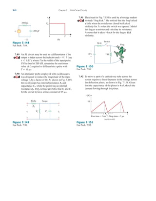
Figure 7.50 shows the step responses in Eqs. (7.63) and (7.64).
v(t) Vsett
u(t)
v(t) L
di
dt
Vs
L
tR
ett
, t
L
R
, t 7 0
v L didt.
i(t)
Vs
R
(1 ett
)u(t)
i(t) c
0, t 6 0
Vs
R
(1 ett
), t 7 0
I0 0,
i(t) i() [i(t0) i()]e(tt0)t
t 0,
t t0
t 7 0.
t 6 0
Figure 7.50
Step responses of an RL circuit with no initial inductor
current: (a) current response, (b) voltage response.
0 t
v(t)
0 t
i(t)
Vs
R
(a) (b)
Vs
ale29559_ch07.qxd 07/08/2008 11:49 AM Page 281](https://image.slidesharecdn.com/fundamentalsofelectriccircuits4thed-220903233817-99157c39/85/Fundamentals_of_Electric_Circuits_4th_Ed-pdf-313-320.jpg)
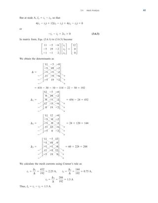
![282 Chapter 7 First-Order Circuits
Find in the circuit of Fig. 7.51 for Assume that the switch
has been closed for a long time.
Solution:
When the resistor is short-circuited, and the inductor acts
like a short circuit. The current through the inductor at (i.e., just
before ) is
Since the inductor current cannot change instantaneously,
When the switch is open. The and resistors are in series,
so that
The Thevenin resistance across the inductor terminals is
For the time constant,
Thus,
Check: In Fig. 7.51, for KVL must be satisfied; that is,
This confirms the result.
5i L
di
dt
[10 15e15t
] c
1
3
(3)(15)e15t
d 10
10 5i L
di
dt
t 7 0,
2 (5 2)e15t
2 3e15t
A, t 7 0
i(t) i() [i(0) i()]ett
t
L
RTh
1
3
5
1
15
s
RTh 2 3 5
i()
10
2 3
2 A
3-
2-
t 7 0,
i(0) i(0
) i(0
) 5 A
i(0
)
10
2
5 A
t 0
t 0
3-
t 6 0,
t 7 0.
i(t)
Example 7.12
Figure 7.51
For Example 7.12.
The switch in Fig. 7.52 has been closed for a long time. It opens at
Find for
Answer: t 7 0.
(6 3e10t
) A for all
t 7 0.
i(t)
t 0.
Practice Problem 7.12
Figure 7.52
For Practice Prob. 7.12.
2 Ω 3 Ω
+
−
10 V
i
t = 0
H
1
3
1.5 H
10 Ω
5 Ω 9 A
t = 0
i
ale29559_ch07.qxd 07/08/2008 11:49 AM Page 282](https://image.slidesharecdn.com/fundamentalsofelectriccircuits4thed-220903233817-99157c39/85/Fundamentals_of_Electric_Circuits_4th_Ed-pdf-314-320.jpg)
![7.6 Step Response of an RL Circuit 283
At switch 1 in Fig. 7.53 is closed, and switch 2 is closed 4 s later.
Find for Calculate i for and t 5 s.
t 2 s
t 7 0.
i(t)
t 0, Example 7.13
Figure 7.53
For Example 7.13.
Solution:
We need to consider the three time intervals and
separately. For switches and are open so that
Since the inductor current cannot change instantly,
For is closed so that the and resistors are
in series. (Remember, at this time, is still open.) Hence, assuming
for now that is closed forever,
Thus,
For is closed; the 10-V voltage source is connected, and
the circuit changes. This sudden change does not affect the inductor
current because the current cannot change abruptly. Thus, the initial
current is
To find let be the voltage at node P in Fig. 7.53. Using KCL,
The Thevenin resistance at the inductor terminals is
and
t
L
RTh
5
22
3
15
22
s
RTh 4 2 6
4 2
6
6
22
3
i()
v
6
30
11
2.727 A
40 v
4
10 v
2
v
6
1 v
180
11
V
v
i(),
i(4) i(4
) 4(1 e8
) 4 A
t 4, S2
4 (0 4)e2t
4(1 e2t
) A, 0 t 4
i(t) i() [i(0) i()]ett
t
L
RTh
5
10
1
2
s
i()
40
4 6
4 A, RTh 4 6 10
S1
S2
6-
4-
0 t 4, S1
i(0
) i(0) i(0
) 0
i 0.
S2
S1
t 6 0,
t 4
t 0, 0 t 4,
4 Ω 6 Ω
+
−
+
−
40 V
10 V
2 Ω 5 H
i
t = 0
t = 4
S1
S2
P
ale29559_ch07.qxd 07/08/2008 11:49 AM Page 283](https://image.slidesharecdn.com/fundamentalsofelectriccircuits4thed-220903233817-99157c39/85/Fundamentals_of_Electric_Circuits_4th_Ed-pdf-315-320.jpg)
![Hence,
We need in the exponential because of the time delay. Thus,
Putting all this together,
At
At
i(5) 2.727 1.273e1.4667
3.02 A
t 5,
i(2) 4(1 e4
) 3.93 A
t 2,
i(t) c
0, t 0
4(1 e2t
), 0 t 4
2.727 1.273e1.4667(t4)
, t 4
2.727 1.273e1.4667(t4)
, t 4
i(t) 2.727 (4 2.727)e(t4)t
, t
15
22
(t 4)
i(t) i() [i(4) i()]e(t4)t
, t 4
284 Chapter 7 First-Order Circuits
Switch in Fig. 7.54 is closed at and switch is closed at
Calculate for all t. Find and
Answer:
i(3) 3.589 A.
i(1) 1.9997 A,
i(t) c
0, t 6 0
2(1 e9t
), 0 6 t 6 2
3.6 1.6e5(t2)
, t 7 2
i(3).
i(1)
i(t)
t 2 s.
S2
t 0,
S1
Practice Problem 7.13
Figure 7.54
For Practice Prob. 7.13.
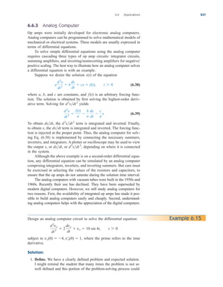
First-Order Op Amp Circuits
An op amp circuit containing a storage element will exhibit first-order
behavior. Differentiators and integrators treated in Section 6.6 are
examples of first-order op amp circuits. Again, for practical reasons,
inductors are hardly ever used in op amp circuits; therefore, the op amp
circuits we consider here are of the RC type.
As usual, we analyze op amp circuits using nodal analysis. Some-
times, the Thevenin equivalent circuit is used to reduce the op amp cir-
cuit to one that we can easily handle. The following three examples
illustrate the concepts. The first one deals with a source-free op amp
circuit, while the other two involve step responses. The three examples
have been carefully selected to cover all possible RC types of op amp
circuits, depending on the location of the capacitor with respect to the
op amp; that is, the capacitor can be located in the input, the output,
or the feedback loop.
7.7
10 Ω
15 Ω
20 Ω
6 A 5 H
t = 0
S1
t = 2
S2
i(t)
ale29559_ch07.qxd 07/08/2008 11:49 AM Page 284](https://image.slidesharecdn.com/fundamentalsofelectriccircuits4thed-220903233817-99157c39/85/Fundamentals_of_Electric_Circuits_4th_Ed-pdf-316-320.jpg)

![■ METHOD 2 Let us apply the short-cut method from Eq. (7.53).
We need to find and Since we
apply KCL at node 2 in the circuit of Fig. 7.55(b) to obtain
or Since the circuit is source free, To find
we need the equivalent resistance across the capacitor terminals.
If we remove the capacitor and replace it by a 1-A current source, we
have the circuit shown in Fig. 7.55(c). Applying KVL to the input loop
yields
Then
and Thus,
as before.
0 (12 0)e10t
12e10t
V, t 7 0
vo(t) vo() [vo(0) vo()]ett
t ReqC 0.1.
Req
v
1
20 k
20,000(1) v 0 1 v 20 kV
Req
t,
v() 0 V.
vo(0
) 12 V.
3
20,000
0 vo(0
)
80,000
0
v(0
) v(0
) 3 V,
t.
vo(0
), vo(),
286 Chapter 7 First-Order Circuits
For the op amp circuit in Fig. 7.56, find for if
Assume that and
Answer: 4e2t
V, t 7 0 .
C 10 mF.
R1 10 k,
Rf 50 k,
v(0) 4 V.
t 7 0
vo
Practice Problem 7.14
Figure 7.56
For Practice Prob. 7.14.
Determine and in the circuit of Fig. 7.57.
Solution:
This problem can be solved in two ways, just like the previous example.
However, we will apply only the second method. Since what we are
looking for is the step response, we can apply Eq. (7.53) and write
(7.15.1)
v(t) v() [v(0) v()]ett
, t 7 0
vo(t)
v(t)
Example 7.15
vo
+
−
R1
Rf
v
+ −
C
+
−
ale29559_ch07.qxd 07/08/2008 11:49 AM Page 286](https://image.slidesharecdn.com/fundamentalsofelectriccircuits4thed-220903233817-99157c39/85/Fundamentals_of_Electric_Circuits_4th_Ed-pdf-318-320.jpg)
![where we need only find the time constant the initial value and
the final value Notice that this applies strictly to the capacitor
voltage due a step input. Since no current enters the input terminals of
the op amp, the elements on the feedback loop of the op amp constitute
an RC circuit, with
(7.15.2)
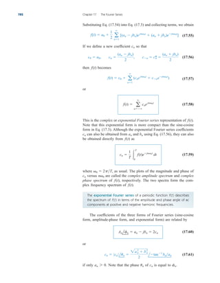
For the switch is open and there is no voltage across the
capacitor. Hence, For we obtain the voltage at node
1 by voltage division as
(7.15.3)
Since there is no storage element in the input loop, remains constant
for all t. At steady state, the capacitor acts like an open circuit so that
the op amp circuit is a noninverting amplifier. Thus,
(7.15.4)
But
(7.15.5)
so that
Substituting and into Eq. (7.15.1) gives
(7.15.6)
From Eqs. (7.15.3), (7.15.5), and (7.15.6), we obtain
(7.15.7)
vo(t) v1(t) v(t) 7 5e20t
V, t 7 0
v(t) 5 [0 (5)]e20t
5(e20t
1) V, t 7 0
v()
t, v(0),
v() 2 7 5 V
v1 vo v
vo() a1
50
20
bv1 3.5 2 7 V
v1
v1
20
20 10
3 2 V
t 7 0,
v(0) 0.
t 6 0,
t RC 50 103
106
0.05
v().
v(0),
t,
7.7 First-Order Op Amp Circuits 287
Figure 7.57
For Example 7.15.
Figure 7.58
For Practice Prob. 7.15.
Find and in the op amp circuit of Fig. 7.58.
Answer: (Note, the voltage across the capacitor and the output voltage
must be both equal to zero, for since the input was zero for all
) 40(e10t
1) u(t) mV.
40(1 e10t
) u(t) mV,
t 6 0.
t 6 0,
vo(t)
v(t) Practice Problem 7.15
vo
v1
+
−
3 V
v
+ −
1 F
50 kΩ
20 kΩ
20 kΩ
+
−
t = 0
10 kΩ
+
−
vo
+
−
4 mV
v
+ −
1 F
100 kΩ
+
−
t = 0
10 kΩ
+
−
ale29559_ch07.qxd 07/08/2008 11:49 AM Page 287](https://image.slidesharecdn.com/fundamentalsofelectriccircuits4thed-220903233817-99157c39/85/Fundamentals_of_Electric_Circuits_4th_Ed-pdf-319-320.jpg)


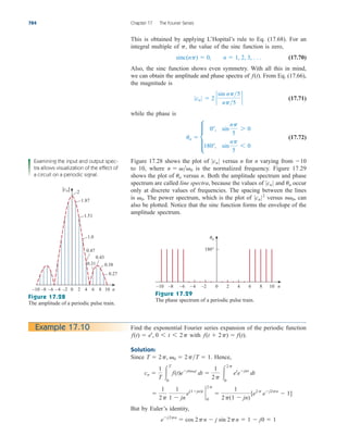
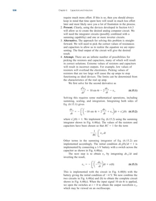
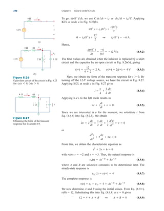
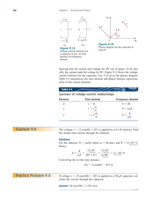
![circuit and not emit light until the voltage across it exceeds a particular
level, say 70 V. When the voltage level is reached, the lamp fires (goes
on), and the capacitor discharges through it. Due to the low resistance
of the lamp when on, the capacitor voltage drops fast and the lamp turns
off. The lamp acts again as an open circuit and the capacitor recharges.
By adjusting we can introduce either short or long time delays into
the circuit and make the lamp fire, recharge, and fire repeatedly every
time constant because it takes a time period to get
the capacitor voltage high enough to fire or low enough to turn off.
The warning blinkers commonly found on road construction sites
are one example of the usefulness of such an RC delay circuit.
t
t (R1 R2)C,
R2,
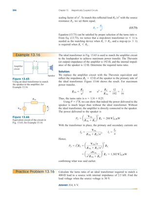
294 Chapter 7 First-Order Circuits
Consider the circuit in Fig. 7.73, and assume that
(a) Calculate the extreme limits of the time con-
stant of the circuit. (b) How long does it take for the lamp to glow for
the first time after the switch is closed? Let assume its largest value.
Solution:
(a) The smallest value for is and the corresponding time constant
for the circuit is
The largest value for is and the corresponding time constant
for the circuit is
Thus, by proper circuit design, the time constant can be adjusted to
introduce a proper time delay in the circuit.
(b) Assuming that the capacitor is initially uncharged, while
But
where as calculated in part (a). The lamp glows when
If at then
or
Taking the natural logarithm of both sides gives
A more general formula for finding is
The lamp will fire repeatedly every seconds if and only if v(t0) 6 v().
t0
t0 t ln
v()
v(t0) v()
t0
t0 t ln
11
4
0.4 ln 2.75 0.4046 s
et0t
4
11
1 et0t
11
4
70 110[1 et0t
] 1
7
11
1 et0t
t t0,
vC(t) 70 V
vC 70 V.
t 0.4 s,
vC(t) vC() [vC(0) vC()]ett
110[1 ett
]
vC() 110.
vC(0) 0,
t (R1 R2)C (1.5 2.5) 106
0.1 106
0.4 s
2.5 M,
R2
t (R1 R2)C (1.5 106
0) 0.1 106
0.15 s
0 ,
R2
R2
0 6 R2 6 2.5 M.
R1 1.5 M,
Example 7.19
ale29559_ch07.qxd 07/08/2008 11:49 AM Page 294](https://image.slidesharecdn.com/fundamentalsofelectriccircuits4thed-220903233817-99157c39/85/Fundamentals_of_Electric_Circuits_4th_Ed-pdf-326-320.jpg)
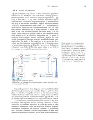
![The coil circuit is an RL circuit like that in Fig. 7.77(b), where R and
L are the resistance and inductance of the coil. When switch in
Fig. 7.77(a) is closed, the coil circuit is energized. The coil current
gradually increases and produces a magnetic field. Eventually the mag-
netic field is sufficiently strong to pull the movable contact in the other
circuit and close switch At this point, the relay is said to be pulled
in. The time interval between the closure of switches and is
called the relay delay time.
Relays were used in the earliest digital circuits and are still used
for switching high-power circuits.
S2
S1
td
S2.
S1
7.9 Applications 297
S2
Coil
Magnetic field
S1
S1
Vs
(a) (b)
Vs
R
L
Figure 7.77
A relay circuit.
Example 7.21
The coil of a certain relay is operated by a 12-V battery. If the coil has
a resistance of and an inductance of 30 mH and the current
needed to pull in is 50 mA, calculate the relay delay time.
Solution:
The current through the coil is given by
where
Thus,
If then
or
etdt
3
8
1 etdt
8
3
50 80[1 etdt
] 1
5
8
1 etdt
i(td) 50 mA,
i(t) 80[1 ett
] mA
t
L
R
30 103
150
0.2 ms
i(0) 0, i()
12
150
80 mA
i(t) i() [i(0) i()]ett
150
ale29559_ch07.qxd 07/08/2008 11:49 AM Page 297](https://image.slidesharecdn.com/fundamentalsofelectriccircuits4thed-220903233817-99157c39/85/Fundamentals_of_Electric_Circuits_4th_Ed-pdf-329-320.jpg)

![300 Chapter 7 First-Order Circuits
4. The singularity functions include the unit step, the unit ramp func-
tion, and the unit impulse functions. The unit step function is
The unit impulse function is
The unit ramp function is
5. The steady-state response is the behavior of the circuit after an
independent source has been applied for a long time. The transient
response is the component of the complete response that dies out
with time.
6. The total or complete response consists of the steady-state
response and the transient response.
7. The step response is the response of the circuit to a sudden appli-
cation of a dc current or voltage. Finding the step response of a
first-order circuit requires the initial value the final value
and the time constant With these three items, we obtain
the step response as
A more general form of this equation is
Or we may write it as
8. PSpice is very useful for obtaining the transient response of a circuit.
9. Four practical applications of RC and RL circuits are: a delay circuit,
a photoflash unit, a relay circuit, and an automobile ignition circuit.
Instantaneous value Final [Initial Final]e(tt0)t
x(t) x() [x(t0
) x()]e(tt0)t
x(t) x() [x(0
) x()]ett
t.
x(),
x(0
),
r(t) b
0, t 0
t, t 0
d(t) c
0, t 6 0
Undefined, t 0
0, t 7 0
u(t) b
0, t 6 0
1, t 7 0
u(t)
Review Questions
7.1 An RC circuit has and The time
constant is:
(a) 0.5 s (b) 2 s (c) 4 s
(d) 8 s (e) 15 s
7.2 The time constant for an RL circuit with
and is:
(a) 0.5 s (b) 2 s (c) 4 s
(d) 8 s (e) 15 s
7.3 A capacitor in an RC circuit with and
is being charged. The time required for the
C 4 F
R 2
L 4 H
R 2
C 4 F.
R 2 capacitor voltage to reach 63.2 percent of its steady-
state value is:
(a) 2 s (b) 4 s (c) 8 s
(d) 16 s (e) none of the above
7.4 An RL circuit has and The time
needed for the inductor current to reach 40 percent
of its steady-state value is:
(a) 0.5 s (b) 1 s (c) 2 s
(d) 4 s (e) none of the above
L 4 H.
R 2
ale29559_ch07.qxd 07/08/2008 11:49 AM Page 300](https://image.slidesharecdn.com/fundamentalsofelectriccircuits4thed-220903233817-99157c39/85/Fundamentals_of_Electric_Circuits_4th_Ed-pdf-332-320.jpg)


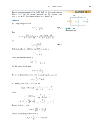
![7.35 Find the solution to the following differential
equations:
(a)
(b)
7.36 Solve for in the following differential equations,
subject to the stated initial condition.
(a)
(b)
7.37 A circuit is described by
(a) What is the time constant of the circuit?
(b) What is the final value of v?
(c) If find for
7.38 A circuit is described by
Find for given that
Section 7.5 Step Response of an RC Circuit
7.39 Calculate the capacitor voltage for and
for each of the circuits in Fig. 7.106.
t 7 0
t 6 0
i(0) 0.
t 7 0
i(t)
di
dt
3i 2u(t)
t 0.
v(t)
v(0) 2,
v(),
4
dv
dt
v 10
2 dvdt v 3u(t), v(0) 6
dvdt v u(t), v(0) 0
v
2
di
dt
3i 0, i(0) 2
dv
dt
2v 0, v(0) 1 V
Problems 305
0 3
2
1
−1
30
20
10
−20
−10
t
v(t)
Figure 7.105
For Prob. 7.27.
7.28 Sketch the waveform represented by
7.29 Sketch the following functions:
(a)
(b)
(c)
7.30 Evaluate the following integrals involving the
impulse functions:
(a)
(b)
7.31 Evaluate the following integrals:
(a)
(b)
7.32 Evaluate the following integrals:
(a)
(b)
(c)
7.33 The voltage across a 10-mH inductor is
Find the inductor current, assuming
that the inductor is initially uncharged.
7.34 Evaluate the following derivatives:
(a)
(b)
(c)
d
dt
[sin 4tu(t 3)]
d
dt
[r(t 6)u(t 2)]
d
dt
[u(t 1)u(t 1)]
20d(t 2) mV.
5
1
(t 6)2
d(t 2)dt
4
0
r(t 1)dt
t
1
u(l)dl
[5d(t) et
d(t) cos 2ptd(t)]dt
e4t2
d(t 2)dt
4t2
cos 2ptd(t 0.5)dt
4t2
d(t 1)dt
z(t) 5 cos 4td(t 1)
y(t) 20e(t1)
u(t)
x(t) 5et
u(t 1)
r(t 3) u(t 4)
i(t) r(t) r(t 1) u(t 2) r(t 2)
+
−
1 Ω
4 Ω
20 V
12 V
+
−
t = 0
v 2 F
(a)
(b)
3 Ω
2 A
4 Ω
+ −
+
− t = 0
2 F
v
Figure 7.106
For Prob. 7.39.
7.40 Find the capacitor voltage for and for
each of the circuits in Fig. 7.107.
t 7 0
t 6 0
ale29559_ch07.qxd 07/08/2008 11:50 AM Page 305](https://image.slidesharecdn.com/fundamentalsofelectriccircuits4thed-220903233817-99157c39/85/Fundamentals_of_Electric_Circuits_4th_Ed-pdf-337-320.jpg)


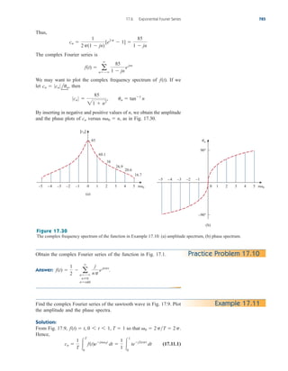
![Underdamped Case ( )
For The roots may be written as
(8.22a)
(8.22b)
where and which is called the damping
frequency. Both and are natural frequencies because they help
determine the natural response; while is often called the undamped
natural frequency, is called the damped natural frequency. The natural
response is
(8.23)
Using Euler’s identities,
(8.24)
we get
(8.25)
Replacing constants and with constants and
we write
(8.26)
With the presence of sine and cosine functions, it is clear that the nat-
ural response for this case is exponentially damped and oscillatory in
nature. The response has a time constant of and a period of
Figure 8.9(c) depicts a typical underdamped response.
[Figure 8.9 assumes for each case that .]
Once the inductor current is found for the RLC series circuit
as shown above, other circuit quantities such as individual element
voltages can easily be found. For example, the resistor voltage is
and the inductor voltage is . The inductor cur-
rent is selected as the key variable to be determined first in order
to take advantage of Eq. (8.1b).
We conclude this section by noting the following interesting, pecu-
liar properties of an RLC network:
1. The behavior of such a network is captured by the idea of damping,
which is the gradual loss of the initial stored energy, as evidenced by
the continuous decrease in the amplitude of the response. The damp-
ing effect is due to the presence of resistance R. The damping factor
determines the rate at which the response is damped. If
then and we have an LC circuit with as the
undamped natural frequency. Since in this case, the response
is not only undamped but also oscillatory. The circuit is said to be
loss-less, because the dissipating or damping element (R) is absent.
By adjusting the value of R, the response may be made undamped,
overdamped, critically damped, or underdamped.
2. Oscillatory response is possible due to the presence of the two
types of storage elements. Having both L and C allows the flow of
a 6 0
11LC
a 0,
R 0,
a
i(t)
vL L didt
vR Ri,
i(t)
i(0) 0
T 2pd.
1a
i(t) eat
(B1 cosdt B2 sin dt)
B2,
B1
j(A1 A2)
(A1 A2)
eat
[(A1 A2) cos dt j(A1 A2) sindt]
i(t) eat
[A1(cosdt j sin dt) A2(cosdt j sindt)]
eju
cosu j sin u, eju
cos u j sin u
i(t) A1e(ajd)t
A2e(ajd)t
eat
(A1ejdt
A2ejdt
)
d
0
d
0
d 20
2
a2
,
j 21
s2 a 2(0
2
a2
) a jd
s1 a 2(0
2
a2
) a jd
a 6 0, C 6 4LR2
.
A 0
8.3 The Source-Free Series RLC Circuit 323
R 0 produces a perfectly sinusoidal
response. This response cannot be
practically accomplished with L and C
because of the inherent losses in them.
See Figs 6.8 and 6.26. An electronic
device called an oscillator can pro-
duce a perfectly sinusoidal response.
Examples 8.5 and 8.7 demonstrate the
effect of varying R.
The response of a second-order circuit
with two storage elements of the same
type, as in Fig. 8.1(c) and (d), cannot
be oscillatory.
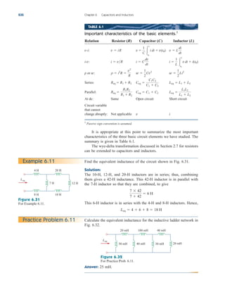
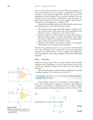
ale29559_ch08.qxd 07/08/2008 11:15 AM Page 323](https://image.slidesharecdn.com/fundamentalsofelectriccircuits4thed-220903233817-99157c39/85/Fundamentals_of_Electric_Circuits_4th_Ed-pdf-355-320.jpg)

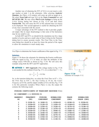
![where is the initial current through the inductor and is the
initial voltage across the capacitor.
For the switch is opened and the voltage source is discon-
nected. The equivalent circuit is shown in Fig. 8.11(b), which is a source-
free series RLC circuit. Notice that the and resistors, which are
in series in Fig. 8.10 when the switch is opened, have been combined to
give in Fig. 8.11(b). The roots are calculated as follows:
or
Hence, the response is underdamped ( ); that is,
(8.4.1)
We now obtain and using the initial conditions. At
(8.4.2)
From Eq. (8.5),
(8.4.3)
Note that is used, because the polarity of v in
Fig. 8.11(b) is opposite that in Fig. 8.8. Taking the derivative of in
Eq. (8.4.1),
Imposing the condition in Eq. (8.4.3) at gives
But from Eq. (8.4.2). Then
Substituting the values of and in Eq. (8.4.1) yields the
complete solution as
i(t) e9t
(cos 4.359t 0.6882 sin 4.359t) A
A2
A1
6 9 4.359A2 1 A2 0.6882
A1 1
6 9(A1 0) 4.359(0 A2)
t 0
e9t
(4.359)(A1 sin 4.359t A2 cos 4.359t)
di
dt
9e9t
(A1 cos 4.359t A2 sin 4.359t)
i(t)
v(0) V0 6 V
di
dt
2
t0
1
L
[Ri(0) v(0)] 2[9(1) 6] 6 A/s
i(0) 1 A1
t 0,
A2
A1
i(t) e9t
(A1 cos 4.359t A2 sin 4.359t)
a 6
s1,2 9 j4.359
s1,2 a 2a2
0
2
9 281 100
a
R
2L
9
2(1
2)
9, 0
1
2LC
1
21
2 1
50
10
R 9
6-
3-
t 7 0,
v(0)
i(0)
8.3 The Source-Free Series RLC Circuit 325
0.5 H
0.02 F
9 Ω
i
(b)
10 V
4 Ω
v
+
−
6 Ω
+
−
i
(a)
v
+
−
Figure 8.10
For Example 8.4.
Figure 8.11
The circuit in Fig. 8.10: (a) for , (b) for .
t 7 0
t 6 0
t = 0
10 V
4 Ω
0.5 H
0.02 F v
+
−
3 Ω
+
−
6 Ω
i
ale29559_ch08.qxd 07/08/2008 11:15 AM Page 325](https://image.slidesharecdn.com/fundamentalsofelectriccircuits4thed-220903233817-99157c39/85/Fundamentals_of_Electric_Circuits_4th_Ed-pdf-357-320.jpg)


![Taking the derivative of in Eq. (8.9.8),
(8.9.10)
Substituting Eq. (8.9.2) into Eq. (8.9.10) at gives
(8.9.11)
From Eqs. (8.9.9) and (8.9.11), we obtain
so that Eq. (8.9.8) becomes
(8.9.12)
From we can obtain other quantities of interest by referring to
Fig. 8.26(b). To obtain i, for example,
(8.9.13)
Notice that in agreement with Eq. (8.9.1).
i(0) 0,
2 6e2t
4e3t
A, t 7 0
i
v
2
1
2
dv
dt
2 6e2t
2e3t
12e2t
6e3t
v,
v(t) 4 12e2t
4e3t
V, t 7 0
A 12, B 4
12 2A 3B 1 2A 3B 12
t 0
dv
dt
2Ae2t
3Be3t
v
8.7 General Second-Order Circuits 341
Practice Problem 8.9
Determine and i for in the circuit of Fig. 8.28. (See comments
about current sources in Practice Prob. 7.5.)
Answer: 3(1 e5t
) A.
12(1 e5t
) V,
t 7 0
v
Figure 8.28
For Practice Prob. 8.9.
Example 8.10
Find for in the circuit of Fig. 8.29.
Solution:
This is an example of a second-order circuit with two inductors. We
first obtain the mesh currents and which happen to be the currents
through the inductors. We need to obtain the initial and final values of
these currents.
For so that For
so that the equivalent circuit is as shown in Fig. 8.30(a). Due
to the continuity of inductor current,
(8.10.1)
(8.10.2)
Applying KVL to the left loop in Fig. 8.30(a) at
7 3i1(0
) vL1
(0
) vo(0
)
t 0
,
vL2
(0
) vo(0
) 1[(i1(0
) i2(0
)] 0
i1(0
) i1(0
) 0, i2(0
) i2(0
) 0
7u(t) 7,
t 7 0,
i1(0
) 0 i2(0
).
7u(t) 0,
t 6 0,
i2,
i1
t 7 0
vo(t)
Figure 8.29
For Example 8.10.
t = 0
3 A
10 Ω 4 Ω
2 H
i
v
+
−
F
1
20
7u(t) V +
−
3 Ω
1 Ω vo
+
−
i1
i2
H
1
2
H
1
5
ale29559_ch08.qxd 07/08/2008 11:16 AM Page 341](https://image.slidesharecdn.com/fundamentalsofelectriccircuits4thed-220903233817-99157c39/85/Fundamentals_of_Electric_Circuits_4th_Ed-pdf-373-320.jpg)

![Figure 8.32
For Practice Prob. 8.10.
where A and B are constants. The steady-state response is
(8.10.10)
From Eqs. (8.10.9) and (8.10.10), we obtain the complete response as
(8.10.11)
We finally obtain A and B from the initial values. From Eqs. (8.10.1)
and (8.10.11),
(8.10.12)
Taking the derivative of Eq. (8.10.11), setting in the derivative,
and enforcing Eq. (8.10.3), we obtain
(8.10.13)
From Eqs. (8.10.12) and (8.10.13), and . Thus,
(8.10.14)
We now obtain from Applying KVL to the left loop in
Fig. 8.30(a) gives
Substituting for in Eq. (8.10.14) gives
(8.10.15)
From Fig. 8.29,
(8.10.16)
Substituting Eqs. (8.10.14) and (8.10.15) into Eq. (8.10.16) yields
(8.10.17)
Note that as expected from Eq. (8.10.2).
vo(0) 0,
vo(t) 2(e3t
e10t
)
vo(t) 1[i1(t) i2(t)]
7
3
10
3
e3t
e10t
i2(t) 7
28
3
16
3
e3t
4e10t
2e3t
5e10t
i1
7 4i1 i2
1
2
di1
dt
1 i2 7 4i1
1
2
di1
dt
i1.
i2
i1(t)
7
3
4
3
e3t
e10t
B 1
A 43
14 3A 10B
t 0
0
7
3
A B
i1(t)
7
3
Ae3t
Be10t
i1ss i1()
7
3
A
8.7 General Second-Order Circuits 343
Practice Problem 8.10
For obtain in the circuit of Fig. 8.32. (Hint: First find
and )
Answer: t 7 0.
8(et
e6t
) V,
v2.
v1
vo(t)
t 7 0,
20u(t) V +
−
1 Ω 1 Ω
+ −
vo
v1 v2
F
1
2 F
1
3
ale29559_ch08.qxd 07/08/2008 11:16 AM Page 343](https://image.slidesharecdn.com/fundamentalsofelectriccircuits4thed-220903233817-99157c39/85/Fundamentals_of_Electric_Circuits_4th_Ed-pdf-375-320.jpg)


![This shows that the derivative is transformed to the phasor domain
as
(9.27)
(Time domain) (Phasor domain)
Similarly, the integral of is transformed to the phasor domain
as
(9.28)
(Time domain) (Phasor domain)
Equation (9.27) allows the replacement of a derivative with respect
to time with multiplication of in the phasor domain, whereas
Eq. (9.28) allows the replacement of an integral with respect to time
with division by in the phasor domain. Equations (9.27) and (9.28)
are useful in finding the steady-state solution, which does not require
knowing the initial values of the variable involved. This is one of the
important applications of phasors.
Besides time differentiation and integration, another important
use of phasors is found in summing sinusoids of the same fre-
quency. This is best illustrated with an example, and Example 9.6
provides one.
The differences between and V should be emphasized:
1. is the instantaneous or time domain representation, while is
the frequency or phasor domain representation.
2. is time dependent, while is not. (This fact is often forgot-
ten by students.)
3. is always real with no complex term, while is generally
complex.
Finally, we should bear in mind that phasor analysis applies only when
frequency is constant; it applies in manipulating two or more sinusoidal
signals only if they are of the same frequency.
V
v(t)
V
v(t)
V
v(t)
v(t)
j
j
V
j
3
v dt
Vj
v(t)
jV
3
dv
dt
jV
v(t)
9.3 Phasors 381
Differentiating a sinusoid is equivalent
to multiplying its corresponding phasor
by j .
Integrating a sinusoid is equivalent to
dividing its corresponding phasor
by j .
Adding sinusoids of the same fre-
quency is equivalent to adding their
corresponding phasors.
Evaluate these complex numbers:
(a)
(b)
Solution:
(a) Using polar to rectangular transformation,
Adding them up gives
40l50 20l30 43.03 j20.64 47.72l25.63
20l30 20[cos(30) j sin(30)] 17.32 j10
40l50 40(cos50 j sin50) 25.71 j30.64
10l30 (3 j4)
(2 j4)(3 j5)*
(40l50 20l30)12
Example 9.3
ale29559_ch09.qxd 07/08/2008 11:54 AM Page 381](https://image.slidesharecdn.com/fundamentalsofelectriccircuits4thed-220903233817-99157c39/85/Fundamentals_of_Electric_Circuits_4th_Ed-pdf-413-320.jpg)
![Taking the square root of this,
(b) Using polar-rectangular transformation, addition, multiplication,
and division,
0.565l160.13
11.66 j9
14 j22
14.73l37.66
26.08l122.47
10l30 (3 j4)
(2 j4)(3 j5)*
8.66 j5 (3 j4)
(2 j4)(3 j5)
(40l50 20l30)12
6.91l12.81
382 Chapter 9 Sinusoids and Phasors
Evaluate the following complex numbers:
(a)
(b)
Answer: (a) (b) 8.293 j7.2.
15.5 j13.67,
10 j5 3l40
3 j4
10l30 j5
[(5 j2)(1 j4) 5l60]*
Practice Problem 9.3
Transform these sinusoids to phasors:
(a)
(b)
Solution:
(a) has the phasor
(b) Since
The phasor form of is
V 4l140 V
v
4 cos(30t 140) V
v 4 sin(30t 50) 4 cos(30t 50 90)
sin A cos(A 90),
I 6l40 A
i 6 cos(50t 40)
v 4 sin(30t 50) V
i 6 cos(50t 40) A
Example 9.4
Express these sinusoids as phasors:
(a)
(b)
Answer: (a) (b) I 4l100 A.
V 7l40 V,
i 4 sin(10t 10) A
v 7 cos(2t 40) V
Practice Problem 9.4
ale29559_ch09.qxd 07/08/2008 11:54 AM Page 382](https://image.slidesharecdn.com/fundamentalsofelectriccircuits4thed-220903233817-99157c39/85/Fundamentals_of_Electric_Circuits_4th_Ed-pdf-414-320.jpg)


![This can be written as
or
(9.53)
If we let then
(9.54)
Since
(9.55)
indicating that Kirchhoff’s voltage law holds for phasors.
By following a similar procedure, we can show that Kirchhoff’s
current law holds for phasors. If we let be the current leav-
ing or entering a closed surface in a network at time t, then
(9.56)
If are the phasor forms of the sinusoids then
(9.57)
which is Kirchhoff’s current law in the frequency domain.
Once we have shown that both KVL and KCL hold in the frequency
domain, it is easy to do many things, such as impedance combination,
nodal and mesh analyses, superposition, and source transformation.
Impedance Combinations
Consider the N series-connected impedances shown in Fig. 9.18. The
same current I flows through the impedances. Applying KVL around
the loop gives
(9.58)
V V1 V2 p VN I(Z1 Z2 p ZN)
9.7
I1 I2 p In 0
i1, i2, p , in,
I1, I2, p , In
i1 i2 p in 0
i1, i2, p , in
V1 V2 p Vn 0
ejt
0,
Re[(V1 V2 p Vn)ejt
] 0
Vk Vmkejuk
,
Re[(Vm1eju1
Vm2eju2
p Vmnejun
)ejt
] 0
Re(Vm1eju1
ejt
) Re(Vm2eju2
ejt
) p Re(Vmnejun
ejt
) 0
390 Chapter 9 Sinusoids and Phasors
+ − + − + −
+
−
I Z1
Zeq
Z2 ZN
V1
V
V2 V
N
Figure 9.18
N impedances in series.
The equivalent impedance at the input terminals is
or
(9.59)
Zeq Z1 Z2 p ZN
Zeq
V
I
Z1 Z2 p ZN
ale29559_ch09.qxd 07/08/2008 11:54 AM Page 390](https://image.slidesharecdn.com/fundamentalsofelectriccircuits4thed-220903233817-99157c39/85/Fundamentals_of_Electric_Circuits_4th_Ed-pdf-422-320.jpg)


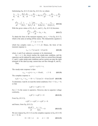
![(b) remains the same as in Eq. (9.15.4) but and are in
parallel. Assuming an RC parallel combination,
By equating the real and imaginary parts, we obtain
We have assumed a parallel RC combination which works in
this case.
5. Evaluate. Let us now use PSpice to see if we indeed have the
correct equalities. Running PSpice with the equivalent circuits,
an open circuit between the “bridge” portion of the circuit,
and a 10-volt input voltage yields the following voltages at the
ends of the “bridge” relative to a reference at the bottom of
the circuit:
FREQ VM($N_0002) VP($N_0002)
2.000E+03 9.993E+00 -8.634E-03
2.000E+03 9.993E+00 -8.637E-03
Since the voltages are essentially the same, then no measurable
current can flow through the “bridge” portion of the circuit for
any element that connects the two points together and we have a
balanced bridge, which is to be expected. This indicates we have
properly determined the unknowns.
There is a very important problem with what we have done!
Do you know what that is? We have what can be called an
ideal, “theoretical” answer, but one that really is not very good
in the real world. The difference between the magnitudes of the
upper impedances and the lower impedances is much too large
and would never be accepted in a real bridge circuit. For
greatest accuracy, the overall magnitude of the impedances must
at least be within the same relative order. To increase the
accuracy of the solution of this problem, I would recommend
increasing the magnitude of the top impedances to be in the
range of to One additional real-world comment:
the size of these impedances also creates serious problems in
making actual measurements, so the appropriate instruments
must be used in order to minimize their loading (which would
change the actual voltage readings) on the circuit.
6. Satisfactory? Since we solved for the unknown terms and then
tested to see if they woked, we validated the results. They can
now be presented as a solution to the problem.
1.5 M
.
500 k
1.356
2p(2000)(5.9172
1.3562
)
2.852 mF
Cx
Imag(Zx)
[Real(Zx)2
Imag(Zx)2
]
Rx
Real(Zx)2
Imag(Zx)2
Real(Zx)
5.9932
1.3562
5.993
6.3 M
Rx
1
jCx
Rx
1 jRxCx
Zx (5.993 j1.356) M
Xx
Rx
Zx
9.8 Applications 401
ale29559_ch09.qxd 07/08/2008 11:54 AM Page 401](https://image.slidesharecdn.com/fundamentalsofelectriccircuits4thed-220903233817-99157c39/85/Fundamentals_of_Electric_Circuits_4th_Ed-pdf-433-320.jpg)
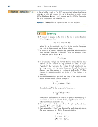


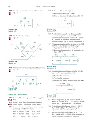
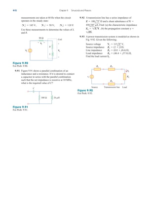


![420 Chapter 10 Sinusoidal Steady-State Analysis
From Eqs. (10.4.5) and (10.4.6), we obtain the matrix equation
We obtain the following determinants
Current is obtained as
The required voltage is
■ METHOD 2 We can use MATLAB to solve Eqs. (10.4.1) to
(10.4.4). We first cast the equations as
(10.4.7a)
or
By inverting A, we can obtain I as
(10.4.7b)
We now apply MATLAB as follows:
A = [(8-j*2) j*2 -8 0;
0 1 0 0;
-8 -j*5 (8-j*4) (6+j*5);
0 0 -1 1];
B = [10 -3 0 4]’;
I = inv(A)*B
I =
0.2828 - 3.6069i
-3.0000
-1.8690 - 4.4276i
2.1310 - 4.4276i
Vo = -2*j*(I(1) - I(2))
Vo =
-7.2138 - 6.5655i
as obtained previously.
I A1
B
AI B
D
8 j2 j2 8 0
0 1 0 0
8 j5 8 j4 6 j5
0 0 1 1
T D
I1
I2
I3
I4
T D
10
3
0
4
T
7.2134 j6.568 9.756l222.32 V
Vo j2(I1 I2) j2(3.618l274.5 3)
V0
I1
¢1
¢
58 j186
50 j20
3.618l274.5 A
I1
58 j186
¢1 `
10 j6 8
24 j35 14 j
` 140 j10 j84 6 192 j280
¢ `
8 j2 8
8 14 j
` 112 j8 j28 2 64 50 j20
c
8 j2 8
8 14 j
d B
I1
I3
R B
10 j6
24 j35
R
ale29559_ch10.qxd 07/08/2008 11:58 AM Page 420](https://image.slidesharecdn.com/fundamentalsofelectriccircuits4thed-220903233817-99157c39/85/Fundamentals_of_Electric_Circuits_4th_Ed-pdf-452-320.jpg)
![From Eqs. (10.5.4) and (10.5.5),
Expressing in terms of gives
(10.5.6)
Substituting Eqs. (10.5.5) and (10.5.6) into Eq. (10.5.3), we get
or
Current is obtained as
(10.5.7)
From Eqs. (10.5.2) and (10.5.7), we write
which agrees with what we got in Example 10.3. It should be noted
that applying the superposition theorem is not the best way to solve
this problem. It seems that we have made the problem twice as hard
as the original one by using superposition. However, in Example 10.6,
superposition is clearly the easiest approach.
Io I¿
o I–
o 5 j3.529 6.12l144.78 A
I–
o I2 2.647 j1.176
I–
o
I2
90 j40
34
2.647 j1.176
(8 j8)[(2 j2)I2 5] j50 j2I2 0
I1 (2 j2)I2 5
I2
I1
(4 j4)I2 j2I1 j10 0
422 Chapter 10 Sinusoidal Steady-State Analysis
Find current in the circuit of Fig. 10.8 using the superposition
theorem.
Answer: 3.582l65.45 A.
Io
Practice Problem 10.5
Example 10.6
2 H 1 Ω 4 Ω
0.1 F 5 V
+
−
+
−
10 cos 2t V 2 sin 5t A
−
+ vo
Figure 10.13
For Example 10.6.
Solution:
Since the circuit operates at three different frequencies for the
dc voltage source), one way to obtain a solution is to use superposition,
which breaks the problem into single-frequency problems. So we let
(10.6.1)
vo v1 v2 v3
( 0
Find of the circuit of Fig. 10.13 using the superposition theorem.
vo
ale29559_ch10.qxd 07/08/2008 11:58 AM Page 422](https://image.slidesharecdn.com/fundamentalsofelectriccircuits4thed-220903233817-99157c39/85/Fundamentals_of_Electric_Circuits_4th_Ed-pdf-454-320.jpg)

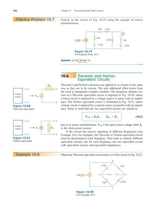
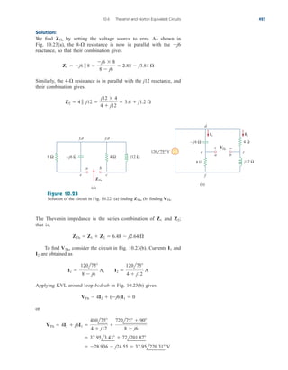


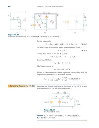
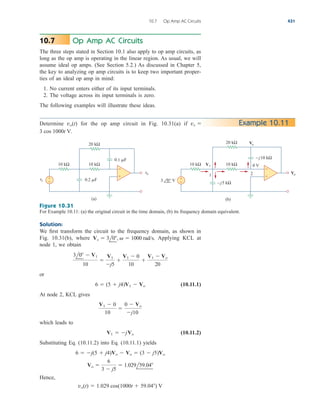
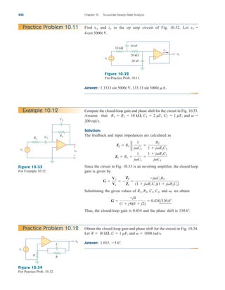


![exchanged the positions of the voltage-controlled current source G1
and the impedance. Notice that the current of G1 flows
from node 1 to node 3, while the controlling voltage is across the
capacitor C2, as required in Fig. 10.38. The attributes of pseudo-
components VPRINT1 are set as shown. As a single-frequency
analysis, we select Analysis/Setup/AC Sweep and enter
and .
After saving the schematic, we select Analysis/Simulate
to simulate the circuit. When this is done, the output file
includes
FREQ VM(1) VP(1)
1.592E–01 2.708E+00 –5.673E+01
FREQ VM(3) VP(3)
1.592E-01 4.468E+00 –1.026E+02
from which we obtain,
5. Evaluate. One of the most important lessons to be learned is
that when using programs such as PSpice you still need to
validate the answer. There are many opportunities for making a
mistake, including coming across an unknown “bug” in PSpice
that yields incorrect results.
So, how can we validate this solution? Obviously, we can
rework the entire problem with nodal analysis, and perhaps
using MATLAB, to see if we obtain the same results. There is
another way we will use here: write the nodal equations and
substitute the answers obtained in the PSpice solution, and see
if the nodal equations are satisfied.
The nodal equations for this circuit are given below. Note
we have substituted into the dependent source.
Now, to check the answer, we substitute the PSpice answers into
this.
6. Satisfactory? Although we used only the equation from node 1
to check the answer, this is more than satisfactory to validate the
answer from the PSpice solution. We can now present our work
as a solution to the problem.
3 j0.0003 [Answer checks]
4.984 j1.4272 1.9842 j1.4269
5.184l15.98 2.444l35.72
1.9144l40.76 2.708l56.74 0.3536l45 6.911l80.72
1.9144l40.76 V1 0.3536l45 V2 3
(1.45 j1.25)V1 (0.25 j0.25)V2 3
(0.25 j0.25 j0.5)V2 3
(1 j 0.25 j0.25 0.2 j0.5)V1
3
V1 0
1
V1 0
j1
V1 V2
2 j2
0.2V1
V1 V2
j2
0
V1 Vx
V1 2.708l56.74 V and V2 6.911l80.72 V
Final Freq 0.15916
Total Pts 1, Start Freq 0.15916,
2 j2
436 Chapter 10 Sinusoidal Steady-State Analysis
ale29559_ch10.qxd 07/08/2008 11:58 AM Page 436](https://image.slidesharecdn.com/fundamentalsofelectriccircuits4thed-220903233817-99157c39/85/Fundamentals_of_Electric_Circuits_4th_Ed-pdf-468-320.jpg)
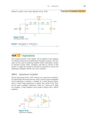


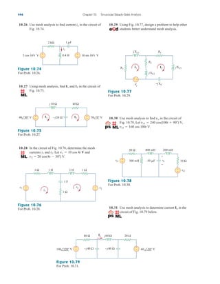

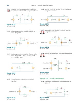
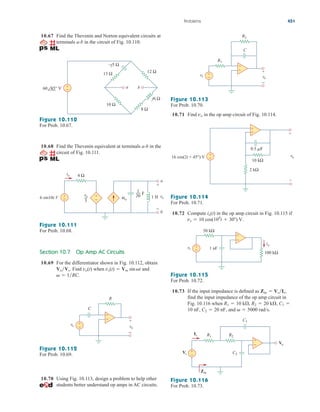

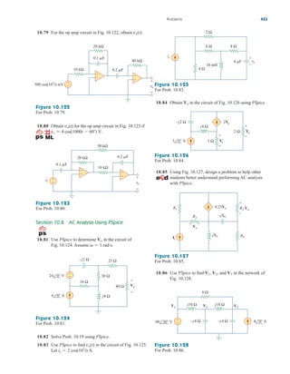


![Introduction
Our effort in ac circuit analysis so far has been focused mainly on cal-
culating voltage and current. Our major concern in this chapter is
power analysis.
Power analysis is of paramount importance. Power is the most
important quantity in electric utilities, electronic, and communication
systems, because such systems involve transmission of power from one
point to another. Also, every industrial and household electrical
device—every fan, motor, lamp, pressing iron, TV, personal computer—
has a power rating that indicates how much power the equipment
requires; exceeding the power rating can do permanent damage to an
appliance. The most common form of electric power is 50- or 60-Hz
ac power. The choice of ac over dc allowed high-voltage power trans-
mission from the power generating plant to the consumer.
We will begin by defining and deriving instantaneous power and
average power. We will then introduce other power concepts. As prac-
tical applications of these concepts, we will discuss how power is
measured and reconsider how electric utility companies charge their
customers.
Instantaneous and Average Power
As mentioned in Chapter 2, the instantaneous power p(t) absorbed by
an element is the product of the instantaneous voltage v(t) across the
element and the instantaneous current i(t) through it. Assuming the pas-
sive sign convention,
(11.1)
p(t) v(t)i(t)
11.2
11.1
458 Chapter 11 AC Power Analysis
The instantaneous power (in watts) is the power at any instant of time.
It is the rate at which an element absorbs energy.
Consider the general case of instantaneous power absorbed by an
arbitrary combination of circuit elements under sinusoidal excitation,
as shown in Fig. 11.1. Let the voltage and current at the terminals of
the circuit be
(11.2a)
(11.2b)
where and are the amplitudes (or peak values), and and are
the phase angles of the voltage and current, respectively. The instanta-
neous power absorbed by the circuit is
(11.3)
We apply the trigonometric identity
(11.4)
cos A cos B
1
2
[cos(A B) cos(A B)]
p(t) v(t)i(t) VmIm cos(t uv) cos(t ui)
ui
uv
Im
Vm
i(t) Im cos(t ui)
v(t) Vm cos(t uv)
Sinusoidal
source
Passive
linear
network
i(t)
+
−
v(t)
We can also think of the instantaneous
power as the power absorbed by the
element at a specific instant of time.
Instantaneous quantities are denoted
by lowercase letters.
Figure 11.1
Sinusoidal source and passive linear circuit.
ale29559_ch11.qxd 07/08/2008 12:01 PM Page 458](https://image.slidesharecdn.com/fundamentalsofelectriccircuits4thed-220903233817-99157c39/85/Fundamentals_of_Electric_Circuits_4th_Ed-pdf-490-320.jpg)
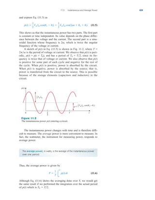
![Substituting p(t) in Eq. (11.5) into Eq. (11.6) gives
(11.7)
The first integrand is constant, and the average of a constant is the same
constant. The second integrand is a sinusoid. We know that the aver-
age of a sinusoid over its period is zero because the area under the
sinusoid during a positive half-cycle is canceled by the area under it
during the following negative half-cycle. Thus, the second term in
Eq. (11.7) vanishes and the average power becomes
(11.8)
Since what is important is the difference
in the phases of the voltage and current.
Note that p(t) is time-varying while P does not depend on time. To
find the instantaneous power, we must necessarily have v(t) and i(t) in
the time domain. But we can find the average power when voltage and
current are expressed in the time domain, as in Eq. (11.8), or when they
are expressed in the frequency domain. The phasor forms of v(t) and i(t)
in Eq. (11.2) are and respectively. P is calculated
using Eq. (11.8) or using phasors V and I. To use phasors, we notice that
(11.9)
We recognize the real part of this expression as the average power P
according to Eq. (11.8). Thus,
(11.10)
Consider two special cases of Eq. (11.10). When the volt-
age and current are in phase. This implies a purely resistive circuit or
resistive load and
(11.11)
where Equation (11.11) shows that a purely resistive cir-
cuit absorbs power at all times. When we have a purely
reactive circuit, and
(11.12)
P
1
2
VmIm cos 90 0
uv ui 90,
0I0 2
I I*.
P
1
2
VmIm
1
2
I2
mR
1
2
0I 02
R
R,
uv ui,
P
1
2
Re[VI*]
1
2
VmIm cos(uv ui)
1
2
VmIm[cos(uv ui) j sin(uv ui)]
1
2
VI*
1
2
VmImluv ui
I Imlui,
V Vmluv
cos(uv ui) cos(ui uv),
P
1
2
VmIm cos(uv ui)
1
2
VmIm
1
T
T
0
cos(2t uv ui) dt
1
2
VmIm cos(uv ui)
1
T
T
0
dt
1
T
T
0
1
2
VmIm cos(2t uv ui) dt
P
1
T
T
0
1
2
VmIm cos(uv ui) dt
460 Chapter 11 AC Power Analysis
ale29559_ch11.qxd 07/08/2008 12:01 PM Page 460](https://image.slidesharecdn.com/fundamentalsofelectriccircuits4thed-220903233817-99157c39/85/Fundamentals_of_Electric_Circuits_4th_Ed-pdf-492-320.jpg)
![Calculate the average power absorbed by an impedance
when a voltage is applied across it.
Solution:
The current through the impedance is
I
V
Z
120l0
30 j70
120l0
76.16l66.8
1.576l66.8 A
V 120l0
Z 30 j70
showing that a purely reactive circuit absorbs no average power. In
summary,
11.2 Instantaneous and Average Power 461
A resistive load (R) absorbs power at all times, while a reactive load
(L or C) absorbs zero average power.
Given that
find the instantaneous power and the average power absorbed by the
passive linear network of Fig. 11.1.
Solution:
The instantaneous power is given by
Applying the trigonometric identity
gives
or
The average power is
which is the constant part of p(t) above.
600 cos 55 344.2 W
P
1
2
VmIm cos(uv ui)
1
2
120(10) cos[45 (10)]
p(t) 344.2 600 cos(754t 35) W
p 600[cos(754t 35) cos 55]
cos A cos B
1
2
[cos(A B) cos(A B)]
p vi 1200 cos(377t 45) cos(377t 10)
v(t) 120 cos(377t 45) V and i(t) 10 cos(377t 10) A
Example 11.1
Calculate the instantaneous power and average power absorbed by the
passive linear network of Fig. 11.1 if
Answer: 1.0606 kW.
1.0606 1.65 cos(20t 10) kW,
v(t) 165 cos(10t 20) V and i(t) 20 sin(10t 60) A
Practice Problem 11.1
Example 11.2
ale29559_ch11.qxd 07/08/2008 12:01 PM Page 461](https://image.slidesharecdn.com/fundamentalsofelectriccircuits4thed-220903233817-99157c39/85/Fundamentals_of_Electric_Circuits_4th_Ed-pdf-493-320.jpg)
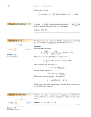
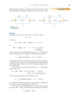
![motor, an antenna, a TV, and so forth. In rectangular form, the
Thevenin impedance and the load impedance are
(11.13a)
(11.13b)
The current through the load is
(11.14)
From Eq. (11.11), the average power delivered to the load is
(11.15)
Our objective is to adjust the load parameters and so that P is
maximum. To do this we set and equal to zero. From
Eq. (11.15), we obtain
(11.16a)
(11.16b)
Setting to zero gives
(11.17)
and setting to zero results in
(11.18)
Combining Eqs. (11.17) and (11.18) leads to the conclusion that for max-
imum average power transfer, must be selected so that
and i.e.,
(11.19)
ZL RL jXL RTh jXTh Z*
Th
RL RTh,
XL XTh
ZL
RL 2R2
Th (XTh XL)2
0P0RL
XL XTh
0P0XL
0P
0RL
0VTh 02
[(RTh RL)2
(XTh XL)2
2RL(RTh RL)]
2[(RTh RL)2
(XTh XL)2
]2
0P
0XL
0VTh 02
RL(XTh XL)
[(RTh RL)2
(XTh XL)2
]2
0P0XL
0P0RL
XL
RL
P
1
2
0I02
RL
0VTh 02
RL2
(RTh RL)2
(XTh XL )2
I
VTh
ZTh ZL
VTh
(RTh jXTh) (RL jXL)
ZL RL jXL
ZTh RTh jXTh
ZL
ZTh
11.3 Maximum Average Power Transfer 465
I
ZL
(a)
VTh
ZTh
(b)
ZL
+
−
Linear
circuit
Figure 11.7
Finding the maximum average power
transfer: (a) circuit with a load, (b) the
Thevenin equivalent.
For maximum average power transfer, the load impedance ZL must
be equal to the complex conjugate of the Thevenin impedance ZTh.
This result is known as the maximum average power transfer theorem
for the sinusoidal steady state. Setting and in
Eq. (11.15) gives us the maximum average power as
(11.20)
In a situation in which the load is purely real, the condition for
maximum power transfer is obtained from Eq. (11.18) by setting
; that is,
(11.21)
RL 2R2
Th X2
Th 0ZTh 0
XL 0
Pmax
0VTh 02
8RTh
XL XTh
RL RTh
When ZL Z*
Th, we say that the load is
matched to the source.
ale29559_ch11.qxd 07/08/2008 12:01 PM Page 465](https://image.slidesharecdn.com/fundamentalsofelectriccircuits4thed-220903233817-99157c39/85/Fundamentals_of_Electric_Circuits_4th_Ed-pdf-497-320.jpg)


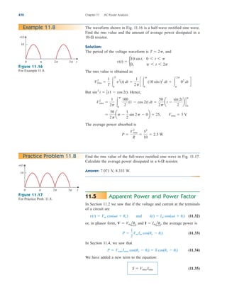


![Solution:
(a) For the rms values of the voltage and current, we write
The complex power is
The apparent power is
(b) We can express the complex power in rectangular form as
Since the real power is
while the reactive power is
(c) The power factor is
It is leading, because the reactive power is negative. The load impedance is
which is a capacitive impedance.
Z
V
I
60l10
1.5l50
40l60
pf cos(60) 0.5 (leading)
Q 38.97 VAR
P 22.5 W
S P jQ,
S 45l60 45[cos(60) j sin(60)] 22.5 j38.97
S 0S0 45 VA
S Vrms I*
rms a
60
22
l10ba
1.5
22
l50b 45l60 VA
Vrms
60
22
l10, Irms
1.5
22
l50
476 Chapter 11 AC Power Analysis
Practice Problem 11.11 For a load, Determine: (a) the
complex and apparent powers, (b) the real and reactive powers, and
(c) the power factor and the load impedance.
Answer: (a) VA, 44 VA, (b) 15.05 W, 41.35 VAR, (c) 0.342
lagging, 94.06 j258.4 .
44l70
Vrms 110l85 V, Irms 0.4l15 A.
Example 11.12 A load Z draws 12 kVA at a power factor of 0.856 lagging from a
120-V rms sinusoidal source. Calculate: (a) the average and reactive pow-
ers delivered to the load, (b) the peak current, and (c) the load impedance.
Solution:
(a) Given that we obtain the power angle as
If the apparent power is VA,
then the average or real power is
P S cosu 12,000 0.856 10.272 kW
S 12,000
u cos1
0.856 31.13.
pf cosu 0.856,
ale29559_ch11.qxd 07/08/2008 12:02 PM Page 476](https://image.slidesharecdn.com/fundamentalsofelectriccircuits4thed-220903233817-99157c39/85/Fundamentals_of_Electric_Circuits_4th_Ed-pdf-508-320.jpg)

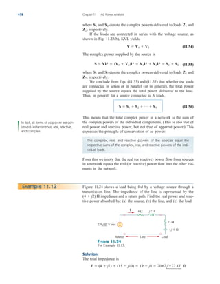
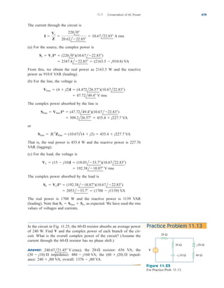


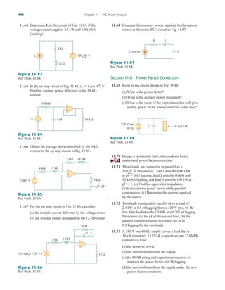


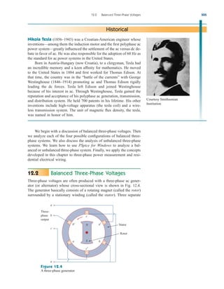

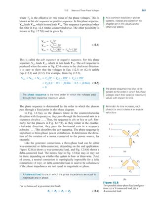


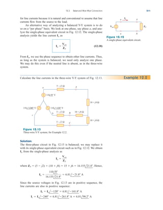

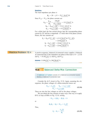

![where is the rms value of the phase current. The total instantaneous
power in the load is the sum of the instantaneous powers in the three
phases; that is,
(12.43)
Applying the trigonometric identity
(12.44)
gives
(12.45)
where
Thus the total instantaneous power in a balanced three-phase system is
constant—it does not change with time as the instantaneous power of
each phase does. This result is true whether the load is Y- or -connected.
This is one important reason for using a three-phase system to generate
and distribute power. We will look into another reason a little later.
Since the total instantaneous power is independent of time, the
average power per phase for either the -connected load or the
Y-connected load is or
(12.46)
and the reactive power per phase is
(12.47)
The apparent power per phase is
(12.48)
The complex power per phase is
(12.49)
where and are the phase voltage and phase current with magni-
tudes and respectively. The total average power is the sum of the
average powers in the phases:
(12.50)
For a Y-connected load, but whereas for a
-connected load, but Thus, Eq. (12.50) applies
for both Y-connected and -connected loads. Similarly, the total reac-
tive power is
(12.51)
Q 3VpIp sinu 3Qp 13VL IL sinu
¢
VL Vp.
IL 13Ip
¢
VL 13Vp,
IL Ip
P Pa Pb Pc 3Pp 3VpIp cosu 13VLIL cosu
Ip,
Vp
Ip
Vp
Sp Pp jQp VpI*
p
Sp VpIp
Qp VpIp sinu
Pp VpIp cosu
p3,
¢
Pp
¢
VpIp c3 cos u cos a 2a
1
2
bcosad 3Vp Ip cos u
a 2t u
cos a cos 240 sin a sin 240]
Vp Ip[3 cos u cos a cos a cos 240 sin a sin 240
cos(2t u 240)]
p Vp Ip[3 cos u cos(2t u) cos(2t u 240)
cos A cos B
1
2
[cos(A B) cos(A B)]
cos(t 120) cos(t u 120)]
cos(t 120) cos(t u 120)
2Vp Ip[cos t cos(t u)
p pa pb pc vANia vBNib vCNic
Ip
520 Chapter 12 Three-Phase Circuits
ale29559_ch12.qxd 07/08/2008 12:05 PM Page 520](https://image.slidesharecdn.com/fundamentalsofelectriccircuits4thed-220903233817-99157c39/85/Fundamentals_of_Electric_Circuits_4th_Ed-pdf-552-320.jpg)


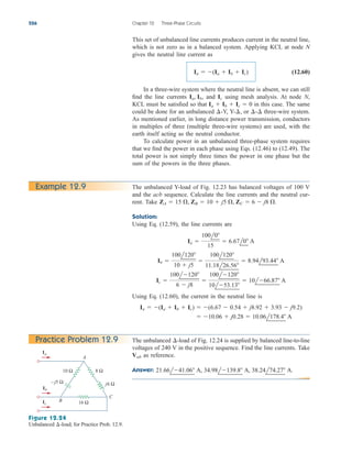
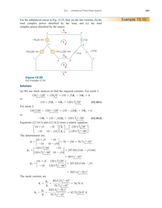


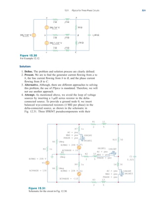
![attributes are inserted to be able to get the required currents
and Since the operating frequency is not given
and the inductances and capacitances should be specified
instead of impedances, we assume so that
Thus,
We select Analysis/Setup/AC Sweep and enter
and Once the
schematic is saved, we select Analysis/Simulate to simulate the
circuit. The output file includes:
FREQ IM(V_PRINT1) IP(V_PRINT1)
1.592E-01 9.106E+00 1.685E+02
FREQ IM(V_PRINT2) IP(V_PRINT2)
1.592E-01 5.959E+00 -1.772E+02
FREQ IM(V_PRINT3) IP(V_PRINT3)
1.592E-01 5.500E+00 1.725E+02
which yields
5. Evaluate. We can check our results by using mesh analysis. Let
the loop aABb be loop 1, the loop bBCc be loop 2, and the loop
ACB be loop 3, with the three loop currents all flowing in the
clockwise direction. We then end up with the following loop
equations:
Loop 1
Loop 2
Loop 3
Using MATLAB to solve this we get,
Z=[(54+10i),(-2-5i),-50;(-2-5i),(4+40i),
-30i;-50,-30i,(50-10i)]
Z=
54.0000+10.0000i-2.0000-5.0000i-50.0000
-2.0000-5.0000i 4.0000+40.0000i 0-30.0000i
-50.0000 0-30.0000i 50.0000-10.0000i
(50)I1 ( j30)I2 (50 j10)I3 0
71.14 j195.46
(2 j5)I1 (4 j40)I2 ( j30)I3 208l110
(54 j10)I1 (2 j5)I2 (50)I3 208l10 204.8 j36.12
IBC 5.5l172.5 A
Iab 5.595l177.2 A, IbB 9.106l168.5 A, and
Final Freq 0.159155.
Start Freq 0.159155,
Total Pts 1,
L
XL
and C
1
XC
f 12p 0.159155 Hz.
1 rad/s
IBC.
Iab, IbB,
532 Chapter 12 Three-Phase Circuits
ale29559_ch12.qxd 07/22/2008 01:38 PM Page 532](https://image.slidesharecdn.com/fundamentalsofelectriccircuits4thed-220903233817-99157c39/85/Fundamentals_of_Electric_Circuits_4th_Ed-pdf-564-320.jpg)
![V=[(204.8+36.12i);(-71.14-195.46i);0]
V=
1.0e+002*
2.0480+0.3612i
-0.7114-1.9546i
0
I=inv(Z)*V
I=
8.9317+2.6983i
0.0096+4.5175i
5.4619+3.7964i
Answer checks
Answer checks
Now to solve for If we assume a small internal impedance
for each source, we can obtain a reasonably good estimate for
Adding in internal resistors of and adding a fourth
loop around the source circuit, we now get
Loop 1
Loop 2
Loop 3
Loop 4
Z=[(54.01+10i),(-2-5i),-50,-0.01;(-2-5i),
(4.01+40i),-30i,-0.01;-50,-30i,(50-10i),
0;-0.01,-0.01,0,0.03]
(0.01)I1 (0.01)I2 (0.03)I4 0
(50)I1 (j30)I2 (50 j10)I3 0
208l110 71.14 j195.46
(2 j5)I1 (4.01 j40)I2 (j30)I3 0.01I4
204.8 j36.12
(54.01 j10)I1 (2 j5)I2 (50)I3 0.01I4 208l10
0.01,
Iab.
Iab.
5.452 j0.722 5.5l172.46 A
IBC I2 I3 (0.0096 j4.518) (5.462 j3.796)
8.922 j1.82 9.106l168.47 A
IbB I1 I2 (8.932 j2.698) (0.0096 j4.518)
12.9 PSpice for Three-Phase Circuits 533
Z=
54.0100+10.0000i -2.0000-5.0000i, -50.0000 -0.0100
-2.0000-5.0000i 4.0100-40.0000i 0-30.0000i 0.0100
-50.0000 0-30.0000i 50.0000-10.0000i 0
-0.0100 -0.0100 0 0.0300
V=[(204.8+36.12i);(-71.14-195.46i);0;0]
ale29559_ch12.qxd 07/22/2008 01:38 PM Page 533](https://image.slidesharecdn.com/fundamentalsofelectriccircuits4thed-220903233817-99157c39/85/Fundamentals_of_Electric_Circuits_4th_Ed-pdf-565-320.jpg)

![unbalanced. The total real power is equal to the algebraic sum of the
two wattmeter readings,
(12.62)
We will show here that the method works for a balanced three-phase
system.
Consider the balanced, wye-connected load in Fig. 12.35. Our
objective is to apply the two-wattmeter method to find the average
power absorbed by the load. Assume the source is in the abc sequence
and the load impedance Due to the load impedance, each
voltage coil leads its current coil by so that the power factor is
We recall that each line voltage leads the corresponding phase voltage
by Thus, the total phase difference between the phase current
and line voltage is and the average power read by
wattmeter is
(12.63)
P1 Re[Vab I*
a] Vab Ia cos(u 30) VL IL cos(u 30)
W1
u 30,
Vab
Ia
30.
cosu.
u,
ZY ZYlu.
PT P1 P2
536 Chapter 12 Three-Phase Circuits
W1
a
b
c
W2
± ±
±
±
Ib
Ic
Ia
ZY ZY
ZY
+
−
Vab
−
+
Vcb
Figure 12.35
Two-wattmeter method applied to a balanced wye load.
Similarly, we can show that the average power read by wattmeter 2 is
(12.64)
We now use the trigonometric identities
(12.65)
to find the sum and the difference of the two wattmeter readings in
Eqs. (12.63) and (12.64):
(12.66)
since Comparing Eq. (12.66) with Eq. (12.50) shows
that the sum of the wattmeter readings gives the total average power,
(12.67)
PT P1 P2
2 cos 30 13.
VL IL2 cos 30 cosu 13VL IL cosu
cosu cos 30 sinu sin 30)
VL IL(cosu cos 30 sinu sin 30
P1 P2 VL IL[cos(u 30) cos(u 30)]
cos(A B) cos A cos B sin A sin B
cos(A B) cos A cos B sin A sin B
P2 Re[Vcb I*
c] Vcb Ic cos(u 30) VL IL cos(u 30)
ale29559_ch12.qxd 07/08/2008 12:05 PM Page 536](https://image.slidesharecdn.com/fundamentalsofelectriccircuits4thed-220903233817-99157c39/85/Fundamentals_of_Electric_Circuits_4th_Ed-pdf-568-320.jpg)
![Similarly,
(12.68)
since Comparing Eq. (12.68) with Eq. (12.51) shows
that the difference of the wattmeter readings is proportional to the total
reactive power, or
(12.69)
From Eqs. (12.67) and (12.69), the total apparent power can be
obtained as
(12.70)
Dividing Eq. (12.69) by Eq. (12.67) gives the tangent of the power fac-
tor angle as
(12.71)
from which we can obtain the power factor as Thus, the
two-wattmeter method not only provides the total real and reactive pow-
ers, it can also be used to compute the power factor. From Eqs. (12.67),
(12.69), and (12.71), we conclude that:
1. If the load is resistive.
2. If the load is inductive.
3. If the load is capacitive.
Although these results are derived from a balanced wye-connected
load, they are equally valid for a balanced delta-connected load. How-
ever, the two-wattmeter method cannot be used for power measurement
in a three-phase four-wire system unless the current through the neu-
tral line is zero. We use the three-wattmeter method to measure the real
power in a three-phase four-wire system.
P2 6 P1,
P2 7 P1,
P2 P1,
pf cosu.
tanu
QT
PT
13
P2 P1
P2 P1
ST 2PT
2
QT
2
QT 13(P2 P1)
2 sin 30 1.
P2 P1 VL IL sinu
VL IL2 sin 30 sinu
cosu cos 30 sinu sin 30)
Vl IL(cosu cos 30 sinu sin 30
P1 P2 VL IL[cos(u 30) cos(u 30)]
12.10 Applications 537
Three wattmeters and are connected, respectively, to phases
a, b, and c to measure the total power absorbed by the unbalanced wye-
connected load in Example 12.9 (see Fig. 12.23). (a) Predict the
wattmeter readings. (b) Find the total power absorbed.
Solution:
Part of the problem is already solved in Example 12.9. Assume that
the wattmeters are properly connected as in Fig. 12.36.
W3
W1, W2, Example 12.13
ale29559_ch12.qxd 07/08/2008 12:05 PM Page 537](https://image.slidesharecdn.com/fundamentalsofelectriccircuits4thed-220903233817-99157c39/85/Fundamentals_of_Electric_Circuits_4th_Ed-pdf-569-320.jpg)
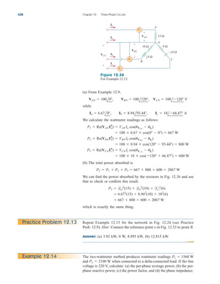


![Since most appliances are designed to operate with 120 V, the lighting
and appliances are connected to the 120-V lines, as illustrated in
Fig. 12.39 for a room. Notice in Fig. 12.37 that all appliances are con-
nected in parallel. Heavy appliances that consume large currents, such
as air conditioners, dishwashers, ovens, and laundry machines, are con-
nected to the 240-V power line.
Because of the dangers of electricity, house wiring is carefully reg-
ulated by a code drawn by local ordinances and by the National Elec-
trical Code (NEC). To avoid trouble, insulation, grounding, fuses, and
circuit breakers are used. Modern wiring codes require a third wire for
a separate ground. The ground wire does not carry power like the neu-
tral wire but enables appliances to have a separate ground connection.
Figure 12.40 shows the connection of the receptacle to a 120-V rms
line and to the ground. As shown in the figure, the neutral line is con-
nected to the ground (the earth) at many critical locations. Although
the ground line seems redundant, grounding is important for many
reasons. First, it is required by NEC. Second, grounding provides a
12.10 Applications 541
Light
pole
Grounded metal
stake
Ground
Wall of
house
Circuit
# 1
120 V
Circuit
# 2
120 V
Circuit
# 3
240 V
Fuse
Fuse Fuses
Switch
Watt-hour meter
Step-down
transformer
Figure 12.37
A 120/240 household power system.
A. Marcus and C. M. Thomson, Electricity for Technicians, 2nd ed. [Englewood Cliffs,
NJ: Prentice Hall, 1975], p. 324.
120 V
lights
120 V
appliance
120 V
lights
120 V
appliance
120 V
120 V
−
+
+
− 240 V
appliance
Black
(hot) B
White
(neutral)
Red (hot)
W
R
Ground
To other houses
Transformer
House
Figure 12.38
Single-phase three-wire residential wiring.
Lamp sockets
Base outlets
120 volts
Ungrounded conductor
Switch
Neutral
Figure 12.39
A typical wiring diagram of a room.
A. Marcus and C. M. Thomson, Electricity for
Technicians, 2nd ed. [Englewood Cliffs, NJ:
Prentice Hall, 1975], p. 325.
ale29559_ch12.qxd 07/08/2008 12:05 PM Page 541](https://image.slidesharecdn.com/fundamentalsofelectriccircuits4thed-220903233817-99157c39/85/Fundamentals_of_Electric_Circuits_4th_Ed-pdf-573-320.jpg)