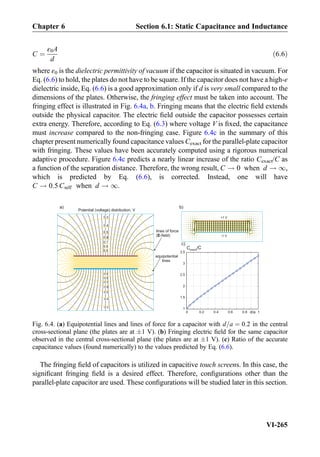
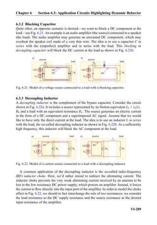
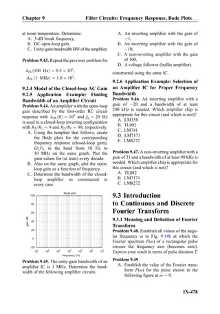
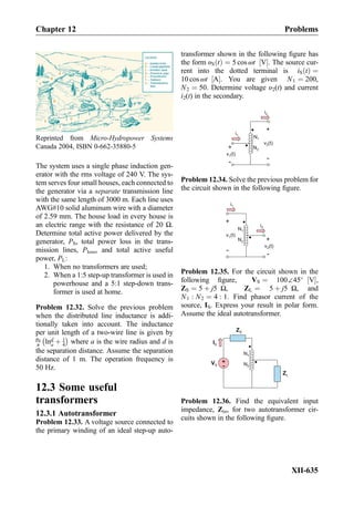
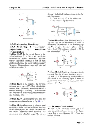
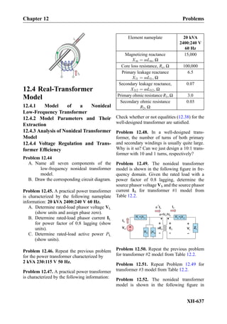
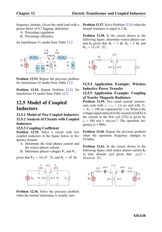
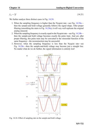
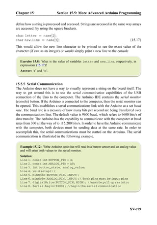
Downloaded 346 times


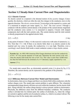
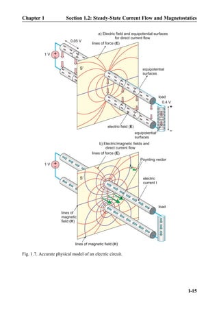
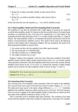
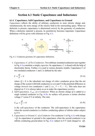
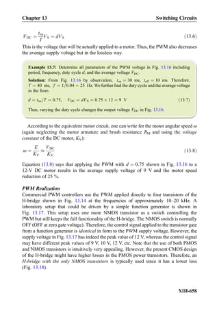
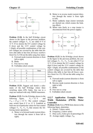
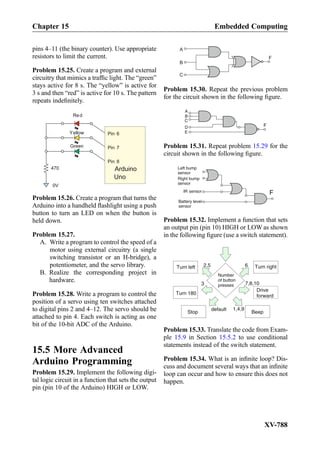
![having the opposite current directions, respectively. The lines of the combined magnetic
field are shown in Fig. 1.7b. They are always perpendicular to the lines of force for the
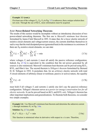
electric field. The magnetic-field magnitude in Fig. 1.7b also has its maximum exactly
between the two conducting wires, at the line connecting its centers.
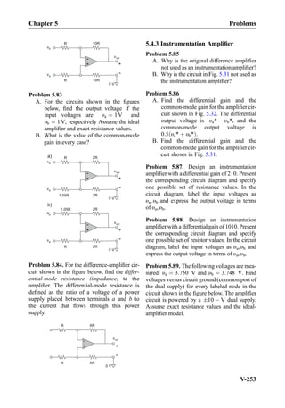
Exercise 1.10: Determine the magnetic-field magnitude in the middle between two
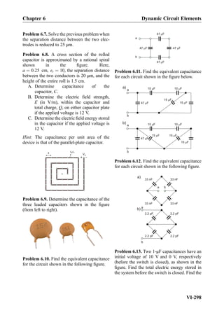
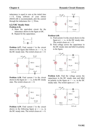
parallel long wires carrying current of Æ1 A each and separated by 2 cm.
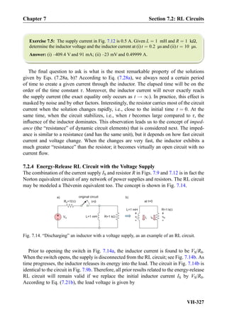
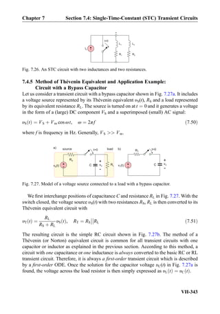
Answer: H ~rð Þ ¼ 31.8 A/m.
Another useful form of Ampere’s law is the magnetic field of an infinite “current
sheet,” i.e., when current flows in a thin conducting sheet in one direction. The sheet may
be thought of as an infinite number of parallel thin wires carrying the same current. If
j [A/m] is the current density per unit of sheet width, then the resulting constant field is
H ¼
1
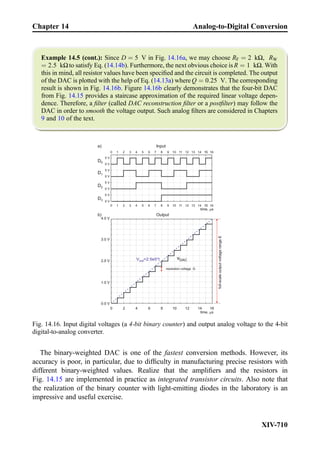
2
j ¼ const ð1:11Þ
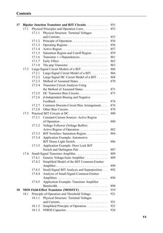
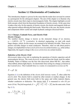
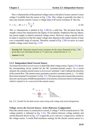
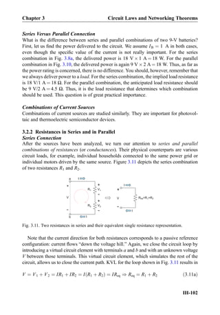
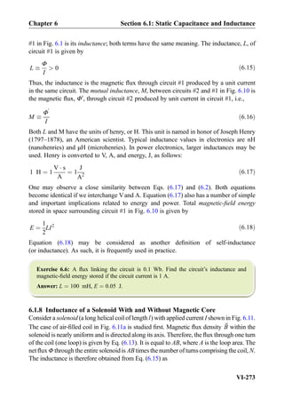
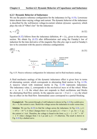
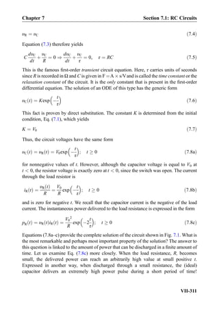
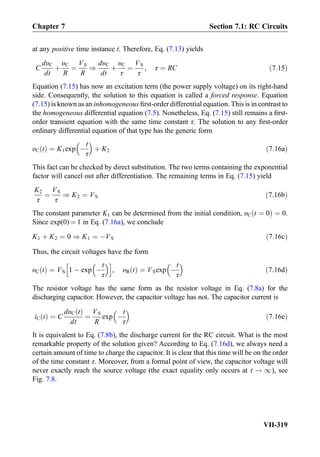
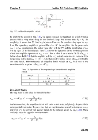
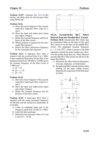
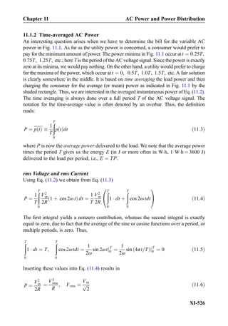
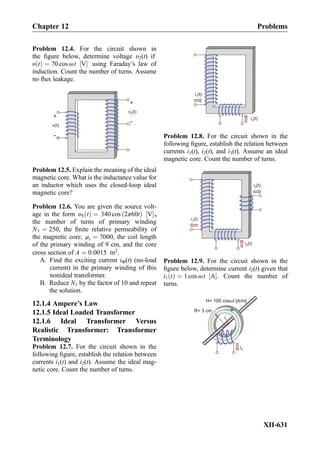
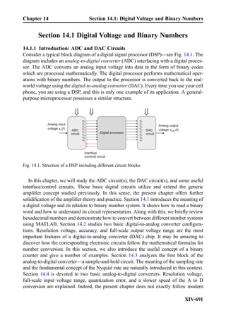
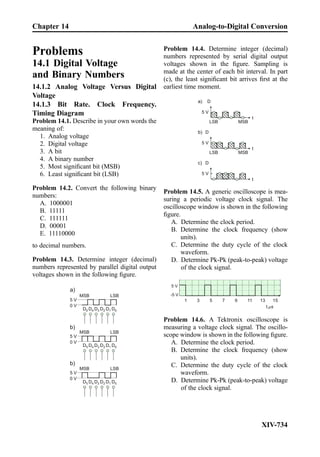
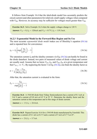
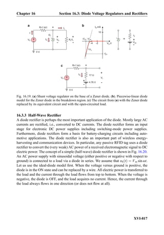
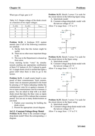
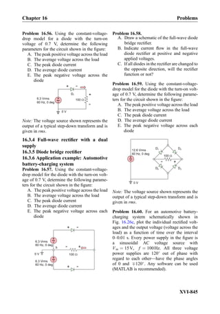
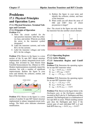
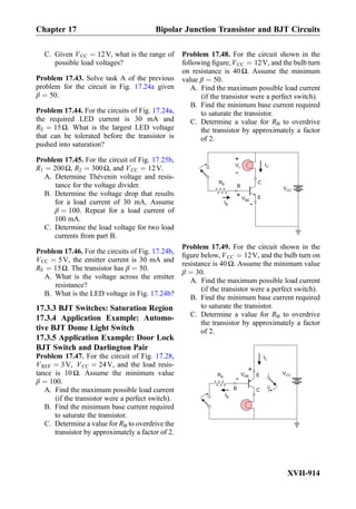
1.2.5 Origin of Electric Power Transfer
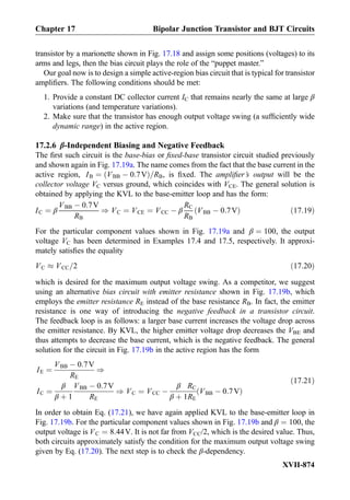
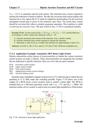
We know from physics classes that electric power P delivered to the load is given by the
product P ¼ VI where V is the voltage across the load and I is the current through it. How
exactly is this power transferred to the load? To answer this question, we assume a
transmission line in the form of two parallel sheets of width W and spacing l shown in
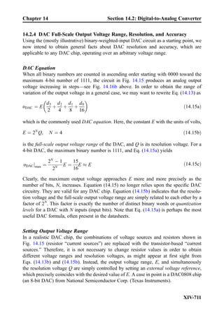
Fig. 1.8. Each sheet carries current density with the magnitude j per unit of sheet length.
When the material conductivity is infinite, the voltage between the two sheets is the
load voltage V. For l=W 1, Eq. (1.9) yields the electric field within the transmission
line,E ¼ V=l. The magnetic field is found using Eq. (1.11). The result isH ¼ jsince both
sheets contribute to the field within the line. Next, we define a vector
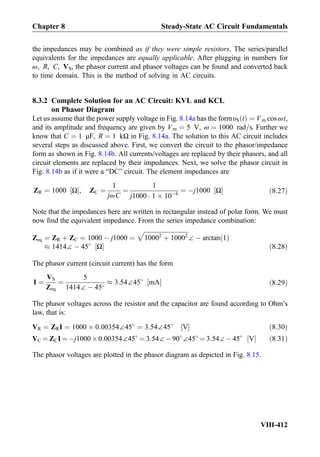
magnetic field (H)
electric field (E)
V
+
-
Poynting vector (S)
to load
W j
Fig. 1.8. Transmission line in the form of two current sheets.
Chapter 1 From Physics to Electric Circuits
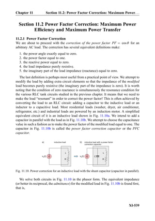
I-16](https://image.slidesharecdn.com/practicalelectricalengineering-160720234734/85/Practical-electrical-engineering-38-320.jpg)

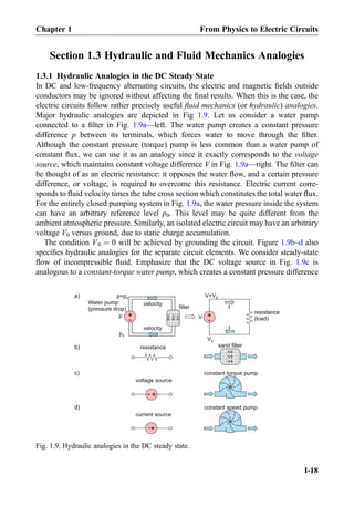
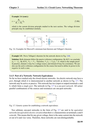
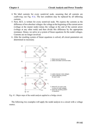
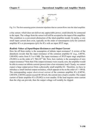
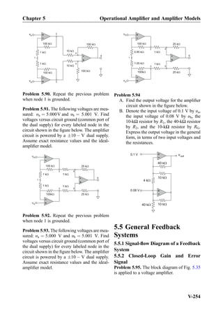
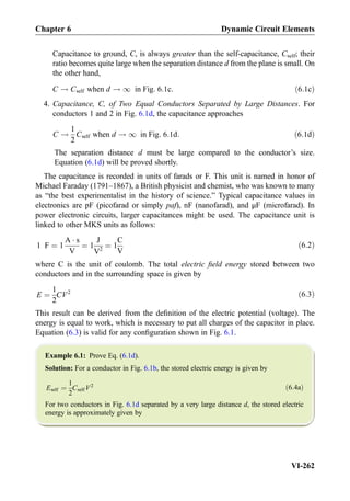
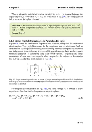
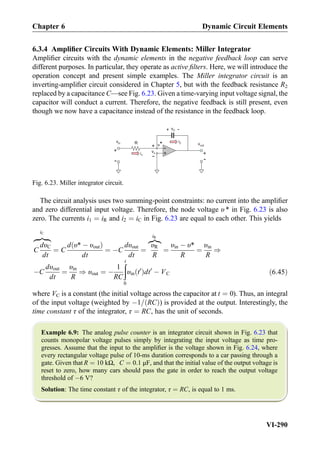
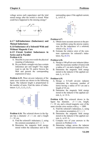
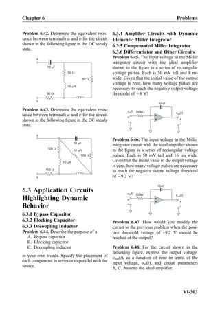
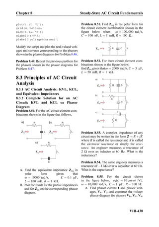
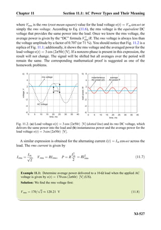
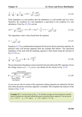
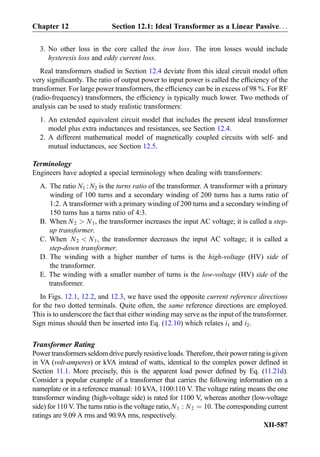
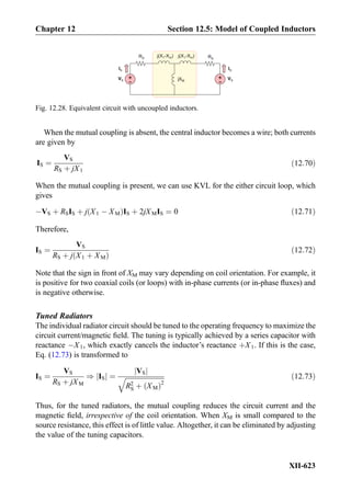
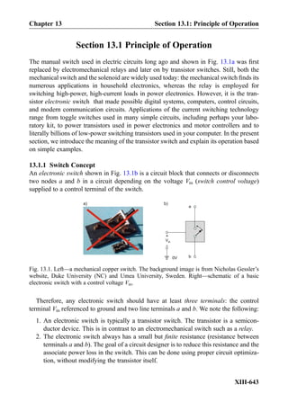
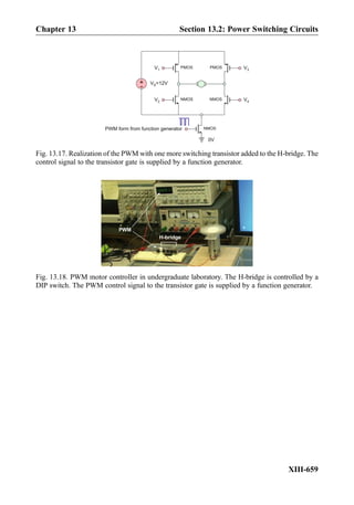
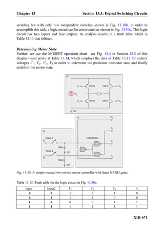
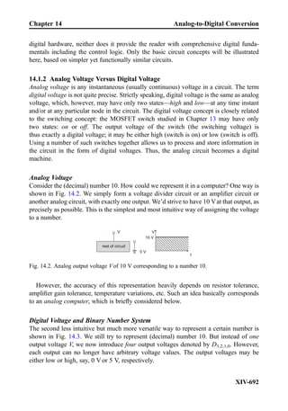
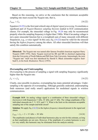
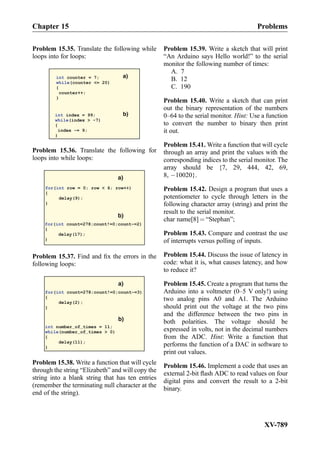
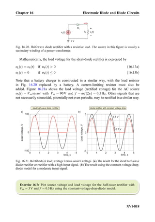
![transformer shown in Fig. 1.10d operates with alternating currents. One mechanical
analogy is a gear transmission or gearbox. In terms of angular speed ω [rad/s] and
developed torque T N Á m½ Š, one has T2 ¼ D2=D1ð ÞT1, and ω2 ¼ D1=D2ð Þω1, where
D1,2 are pitch diameters of gear wheels. Here, torque is the voltage and speed is the
current. D1,2 are similar to the number of turns, N1,2, of the primary and secondary coils of
the transformer, respectively. This analogy ignores the field effect—magnetic coupling
between the coils. Therefore, it will fail in the DC case. A more realistic transformer
analogy is shown in Fig. 1.10e. The model with four pistons transforms power from one
circuit to another in the AC case only. It is drawn for a 1:1 transformer. When a
transformer with a turn ratio of 2:1 is required, the area of output pistons is doubled.
This doubles the output current, but the output voltage (the force) will be halved.
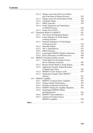
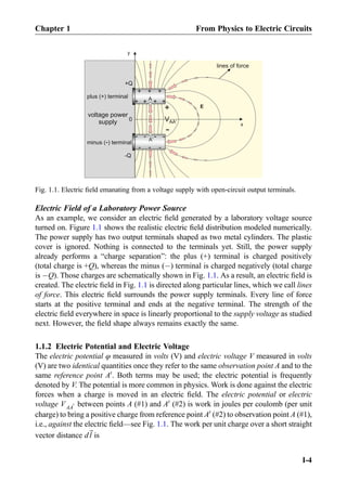
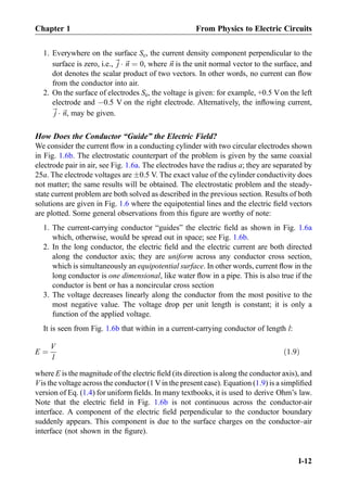
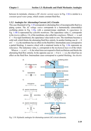
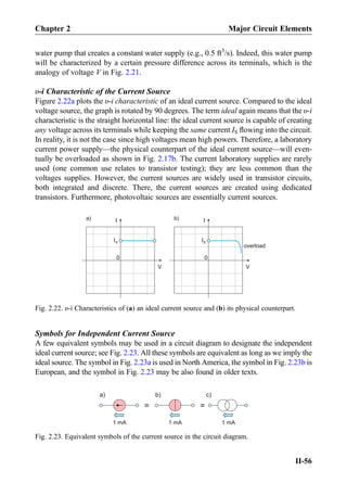
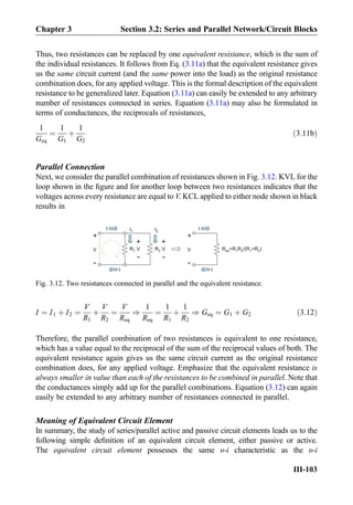
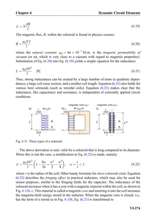
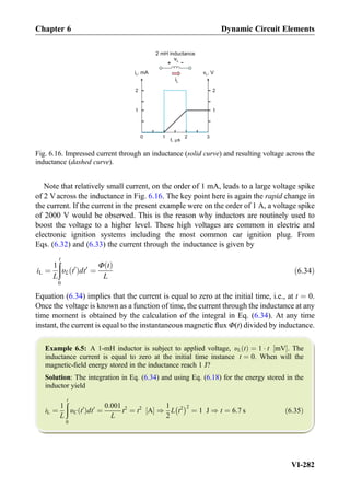
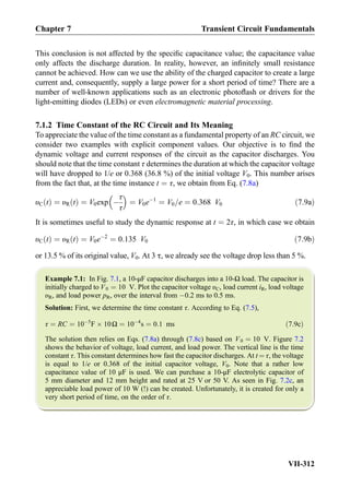
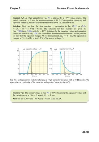
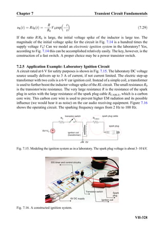
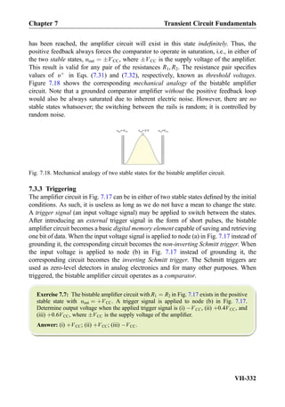
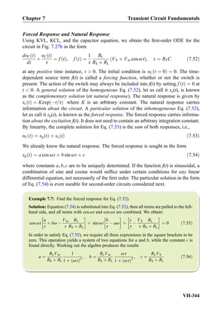
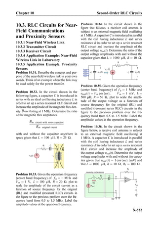
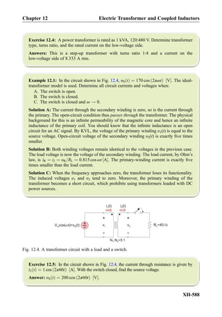
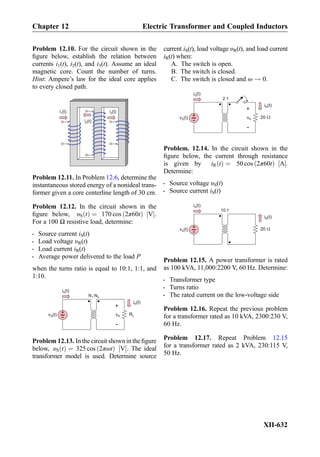
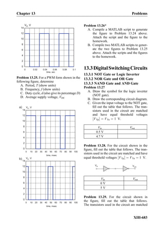
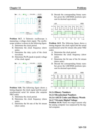
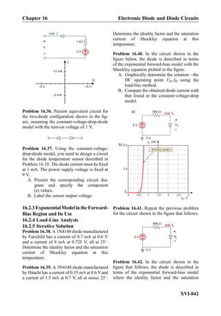
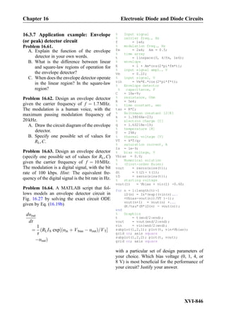
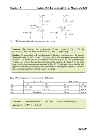
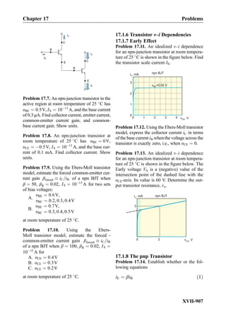
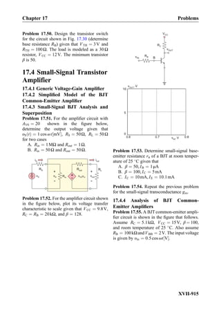
1.3.3 Analogies for Semiconductor Circuit Components
Semiconductor circuit components are similar to fluid valves, which are either externally
controlled or are controlled by the fluid-flow pressure itself. Figure 1.11a shows a hydraulic
analogy for a diode. This picture highlights its major function: a one-way valve. Fig. 1.11b
illustrates the operation of an n-channel metal-oxide-semiconductor field-effect transistor,
or NMOS transistor. This transistor is a valve controlled by a third voltage terminal. For
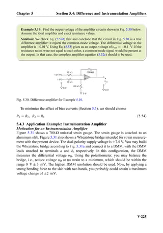
another bipolar junction transistor or BJT in Fig. 1.11c, not only the control voltage but
also the control current is important. In other words, to keep the valve open, we must also
supply a small amount of current (fluid) at the control terminal.
NMOS transistor
a)
semiconductor diode
b)
+ -
higher pressure lower pressure
flexible membrane
control pressure
control voltage
junction transistor
c) control pressure/current
control voltage/current
Fig. 1.11. Analogies for semiconductor circuit components.
Chapter 1 From Physics to Electric Circuits
I-20](https://image.slidesharecdn.com/practicalelectricalengineering-160720234734/85/Practical-electrical-engineering-42-320.jpg)
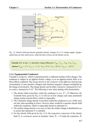
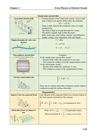
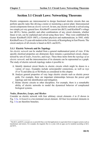
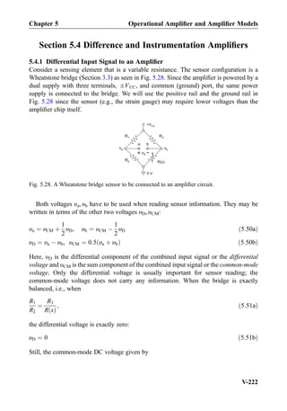
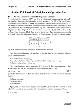
![Summary
Electrostatics
Electric voltage/electric potential VAA
0 ¼ 1 V )Work of 1 J is necessary to bring the 1 C of
charge from point A0
to point A against the field;
VAA
0 ¼ À
ðA
A
0
~E Á d~l for any contour 1, 2, or 3;
~E ~rð Þ ¼ ÀgradV ~rð Þ ¼ À∇V ~rð Þ for potential V ~rð Þ
everywhere in space including materials;
V ¼ lE in uniform fields (most important).
Coulomb force on charge q ~F ¼ q~E [N]
The force is directed along the field for positive charges and
against the field for negative charges
Gauss law Total flux of the electric field through closed surface S times
the permittivity is the total charge enclosed by S.
Q
ε0
¼
ð
S
~E Á ~n dS (ε0 =8.854Â10À12
F/m)
Equipotential conductors Within conductor(s) with applied voltage:
– Electric field is exactly zero;
– Volumetric charge density (C/m3
) is exactly zero.
On surface(s) of conductor(s) with applied voltage:
– Every point has the same voltage (conductor surface is
equipotential surface);
– Surface charge density (C/m2
) exists;
– Emanating electric field is perpendicular to the surface
(tangential field is zero: ~Et ¼ 0)
Outside conductor(s):
– Equipotential lines and lines of force are perpendicular
to each other
Voltage between two wires – Metal wires “guide” the electric field/voltage to a remote
point
– Given the same voltage, charges on wires increase when
their length increases.
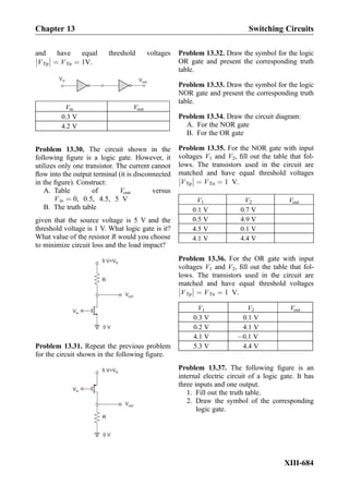
Electrical induction in electrostatics – Conductors 1 and 2 are subject to applied voltages V1, V2;
– Conductor 3 has zero net charge;
– Conductor 3 acquires certain voltage V3;
– Surface charges in conductor 3 are separated as shown in
the figure.
(continued)
Chapter 1 Summary
I-21](https://image.slidesharecdn.com/practicalelectricalengineering-160720234734/85/Practical-electrical-engineering-43-320.jpg)
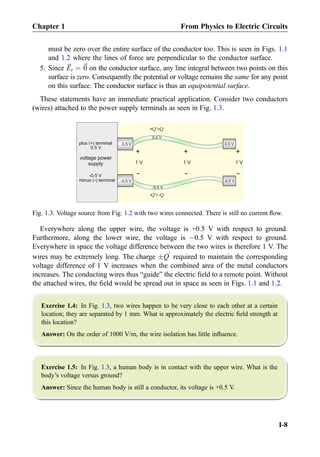
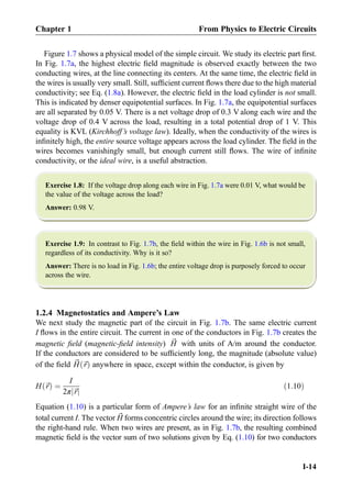
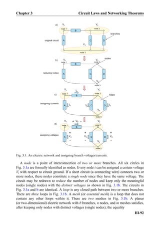
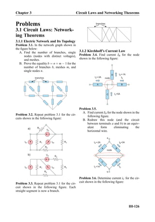
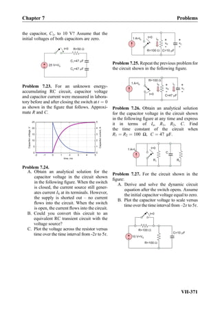
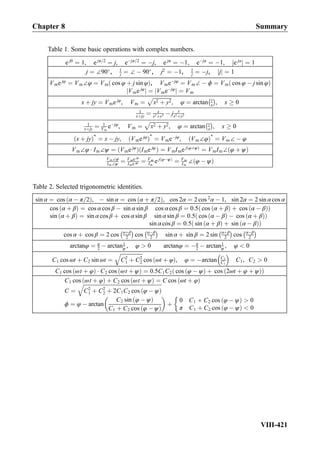
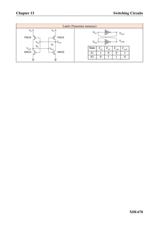
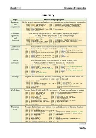
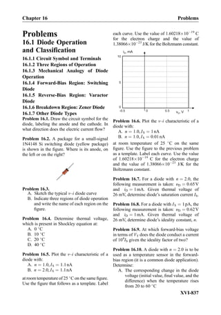
![Problems
1.1 Electrostatics of
Conductors
1.1.2 Electric Potential and Electric
Voltage
1.1.3 Electric Voltage Versus Ground
1.1.4 Equipotential Conductors
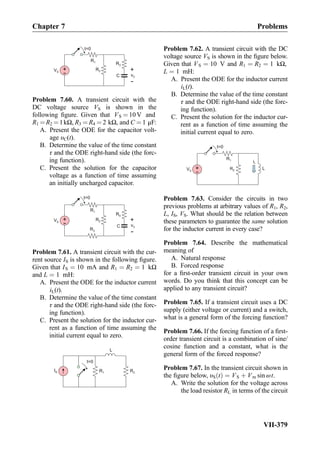
Problem 1.1. Determine voltage (or potential)
VAB and VBA (show units) given that the electric
field between points A and B is uniform and has
the value of 5 V/m. Point A has coordinates
(0, 0); point B has coordinates (1, 1).
E
A
B
Problem 1.2. Determine voltages VAB, VBD,
and VBC given that the electric field shown in
the figure that follows is uniform and has the
value of (A) 10 V/m, (B) 50 V/m, and
(C) 500 V/m.
0 cm
E
5 cm
10 cm
A
B
C
D
Problem 1.3. Assume that the electric field
along a line of force AA0
has the value 1Âl V/
m where 0 l 1 m is the distance along the
line. Find voltage (or potential) VAA
0 .
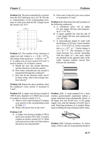
Problem 1.4. The electric potential versus
ground is given in Cartesian coordinates by V
~rð Þ ¼ Àx þ y À z [V]. Determine the
corresponding electric field everywhere in space.
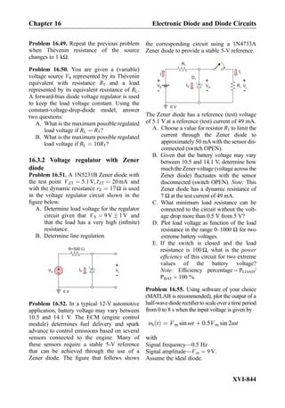
Problem 1.5. The figure below shows the
electric potential distribution across the semi-
conductor pn-junction of a Si diode. What
kinetic energy should the positive charge
(a hole) have in order to climb the potential
hill from anode to cathode given that the hill
“height” (or the built-in voltage of the
pn-junction) is Vbi ¼ 0:7 V? The hole charge
is the opposite of the electron charge. Express
your result in joules.
Vbi
anode cathode
Problem 1.6. Is the electric field shown in the
figure that follows conservative? Justify your
answer.
0
E
1 cm
2 cm
A
B
C
D
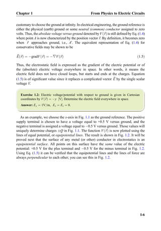
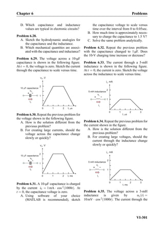
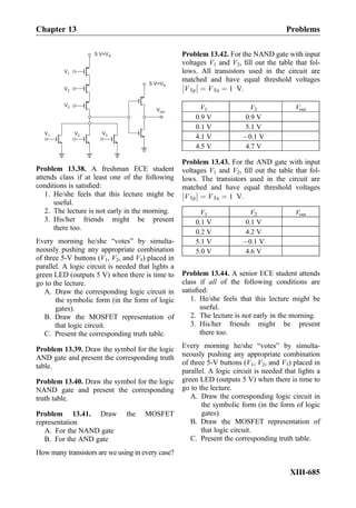
Problem 1.7. List all conditions for voltage and
electric field used in electrostatic problems.
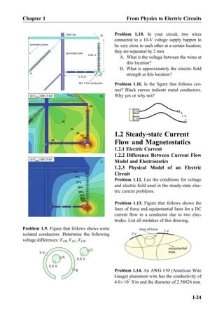
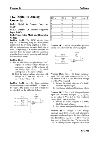
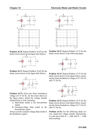
Problem 1.8. The figure below shows a 345 kV
power tower used in MA, USA—front view. It
also depicts electric potential/voltage and elec-
tric field distributions in space:
A. Determine which figure corresponds to
the electric potential and which to the
magnitude of the electric field.
B. Provide a detailed justification of your
answer.
Chapter 1 Problems
I-23](https://image.slidesharecdn.com/practicalelectricalengineering-160720234734/85/Practical-electrical-engineering-45-320.jpg)
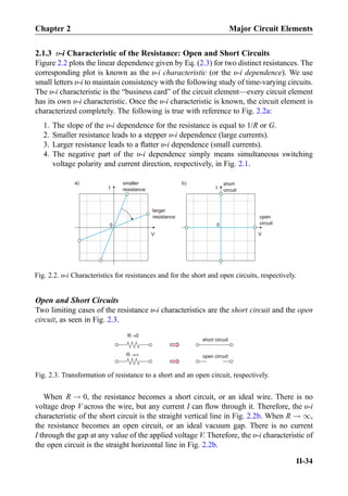
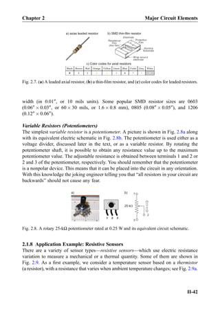
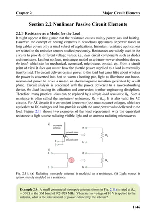
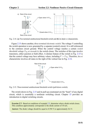
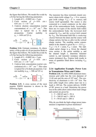
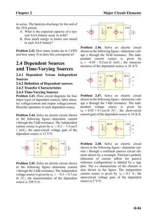
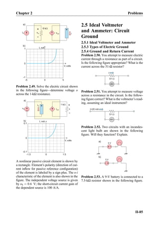
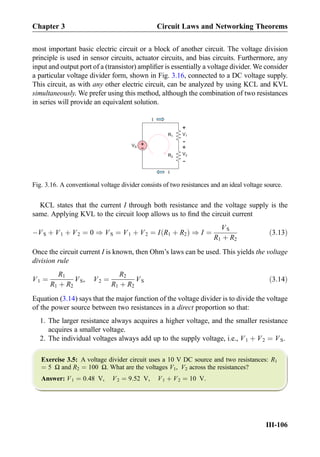
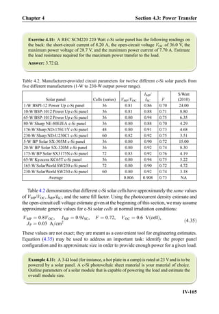
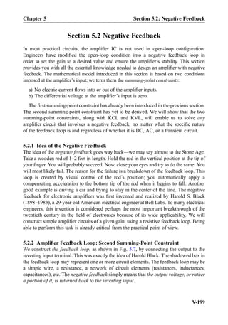
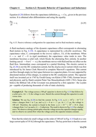
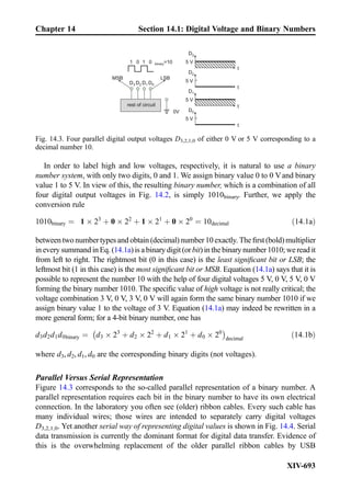
![follows Ohm’s law. It is therefore the nonlinear circuit element. The third element in
Fig. 2.12 corresponds to an ideal (Shockley) diode. The diode does not conduct at negative
applied voltages. At positive voltages, its υ-i characteristic is very sharp (exponential).
The diode is also the nonlinear circuit element. Strictly speaking, the υ-i characteristic of the
incandescent light bulb does not belong to the list of circuit elements due to its limited
applicability. However, the ideal diode is an important nonlinear circuit element. The
nonlinear elements are generally polar (non-symmetric) as Fig. 2.12c shows.
2.2.3 Static Resistance of a Nonlinear Element
Once the υ-i characteristic is known, we can find the static resistance R(V) of the nonlinear
circuit element at any given voltage V0. For example, the υ-i characteristic of the ideal
diode shown in Fig. 2.12c is described by the exponential Shockley equation:
I ¼ IS exp
V
VT
À 1
!
ð2:20Þ
In Eq. (2.20), the constant IS [A] is the diode saturation current. The saturation current is
very small. The constant VT [V] is called the thermal voltage.
Example 2.5: Give a general expression for the diode resistance R(V) using Eq. (2.20)
and find its terminal values atV ! 0andV ! 1, respectively. Then, calculate static diode
resistance R0 and diode current I0 when the voltage across the diode is V0 ¼ 0.55 V.
Assume that IS ¼ 1 Â 10À12
A and VT ¼ 25:7 mV.
Solution: Using Eq. (2.20) we obtain
R Vð Þ ¼
V
IS exp
V
VT
À 1
!
ð2:21Þ
WhenV ! 0, we can use a Taylor series expansion for the exponent. Keeping only the first
nontrivial term, one has exp V=VTð Þ % 1 þ V=VT. Therefore,
R Vð Þ !
VT
IS
when V ! 0 or V=VT 1ð Þ ð2:22Þ
This value is very large, in excess of 1 GΩ. The diode is thus the open circuit with a good
degree of accuracy.
On the other hand, at large V, the exponential factor in Eq. (2.21) greatly increases.
Therefore,
R Vð Þ ! 0 when V ! 1 ð2:23Þ
Chapter 2 Major Circuit Elements
II-48](https://image.slidesharecdn.com/practicalelectricalengineering-160720234734/85/Practical-electrical-engineering-68-320.jpg)

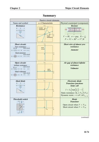
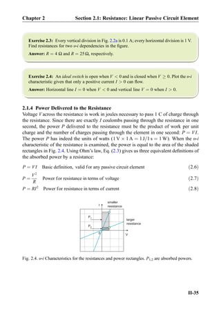
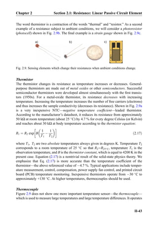
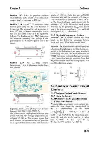
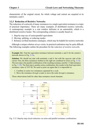
![Active circuit elements
Name and symbol υ–i Characteristic Physical counterpart (component)
Independent voltage
source
Practical voltage source
Independent current
source
Practical current source
Voltage-controlled
voltage source
Transistor
Amplifier
υout ¼ Aυin
A—open-circuit voltage gain
[V/V, V/mV] (dimensionless)
Current-controlled
voltage source
Transistor
Amplifier
υout ¼ Riin
R—transresistance [V/A, V/mA]
(units of resistance, Ω)
Voltage-controlled
current source
Transistor
Amplifier
iout ¼ Gυin
G—transconductance [A/V]
(units of conductance, ΩÀ1
)
Current-controlled
current source
Transistor
Amplifier
iout ¼ Aiin
A—short-circuit current gain
[A/A, A/mA] (dimensionless)
Chapter 2 Summary
II-75](https://image.slidesharecdn.com/practicalelectricalengineering-160720234734/85/Practical-electrical-engineering-95-320.jpg)
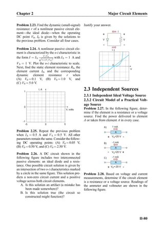
![scale as a function of the value of the unknown
resistance in the range from 10 Ω to 1000 Ω.
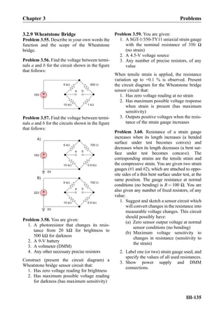
Problem 3.48. A voltage divider circuit with R1
¼ 700 Ω (the fixed resistance) and R2 ¼ 700 Ω
Æ 0:1% (the strain gauge) is used. The voltage
power supply is rated at 4.5 V:
A. Show that voltage across the strain
gauge varies in the range 2.25 V Æ
1.125 mV.
B. Could you derive an analytical formula
that gives the voltage variation across R2
¼ R1 Æ Δ as a linear function of an
arbitrary (but very small) resistance var-
iation Δ?
[Hint: use your calculus background—the
Maclaurin series versus a small parameter].
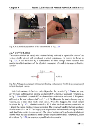
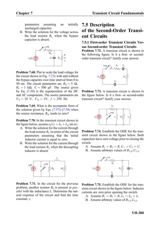
3.2.7 Current Limiter
Problem 3.49. A thermistor is connected to an
ideal voltage power source of 9 V. Determine
the value of the current-limiting resistor
R based on the requirement that the power
delivered to the thermistor should be always
less than 0.1 W. The lowest possible value of
R should be chosen. Consider two cases:
1. Thermistor resistance is exactly 100 Ω.
2. Thermistor resistance changes from
200 Ω to 100 Ω.
R =100WL
+
-9V=VS
R
I
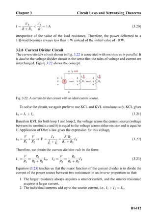
3.2.8 Current Divider Circuit
Problem 3.50. For the circuit shown in the
following figure:
A. Calculate the voltage between terminals
a and b. Show its polarity on the figure.
B. Use the current division principle to cal-
culate branch currents i1, i2.
3 A 1 M 1 M
a
b
i2i1
Problem 3.51. Find branch currents i1, i2 for
the circuit shown in the following figure:
i2i1
+
-10 V 1 kW 1 kW
Problem 3.52. Find branch currents i1, i2 for
the circuit shown in the following figure:
i2i1
3 kW 5 kW10mA
Problem 3.53. Find the voltage between termi-
nals a and b (voltage across the current power
source) for the circuit shown in the following
figure:
5 kW
1 W
5 kW
1 kW1 kW
3A
a
b
Problem 3.54. The voltage source in the circuit
is delivering 0.2 W of electric power. Find R.
+
-10 V
1 kW
RR
Chapter 3 Circuit Laws and Networking Theorems
III-134](https://image.slidesharecdn.com/practicalelectricalengineering-160720234734/85/Practical-electrical-engineering-153-320.jpg)

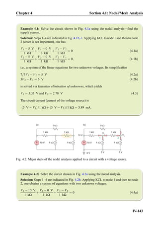
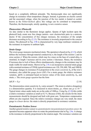
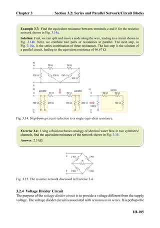
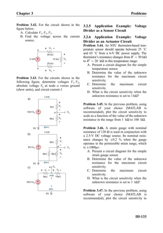
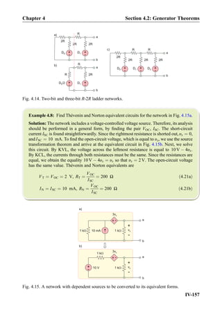
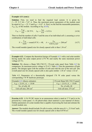
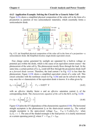
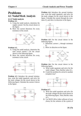
![Example 4.6: The circuit in Fig. 4.10a includes a current-controlled voltage source with
the strength of 4000ix [V]. Find current ix using the source transformation.
Solution: The corresponding circuit transformation is shown in Fig. 4.10b. The circuit with
the current-controlled current source in Fig. 4.10b is solved using KCL and KVL. KCL
written for the bottom node states that the current of 3 mA þ 3ix flows through the
rightmost 1-kΩ resistance (directed down). Since, by KVL, the voltages across both resis-
tances must be equal, one has
3 mA þ 3ix ¼ ix ) ix ¼ À1:5 mA ð4:16Þ
Alternatively, one might convert the independent current source to the independent voltage
source. However, this method would hide ix.
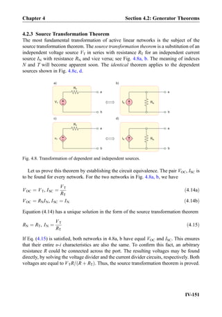
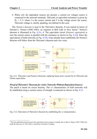
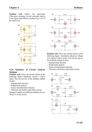
4.2.4 Thévenin’s and Norton’s Theorems: Proof Without Dependent
Sources
The origin of The´venin’s theorem is due to Léon Charles Thévenin, a French engineer
(1857–1926). The theorem is illustrated in Fig. 4.11a, b and can be expressed in the
following form:
1. Any linear network with independent voltage and current sources, dependent linear
sources, and resistances, as shown in Fig. 4.11a, can be replaced by a simple
equivalent network: a voltage source VT in series with resistance RT.
2. The equivalent network in Fig. 4.11b is called the The´venin equivalent.
3. Voltage VT is the open-circuit voltage VOC of the original network.
4. When dependent sources are not present, Thévenin resistance RT is an equivalent
resistance Req of the original network with all independent sources turned off
(voltage sources are replaced by short circuits and current sources by open circuits).
5. When both dependent and independent sources are present, the independent sources
are not turned off. Resistance RT is given by RT ¼ VOC=ISC, where ISC is the short-
circuit current of the original network.
a)
3 mA 1 kW
1 kW
b)
+
- 4000ix
ix
3 mA 1 kW 4ix
ix
1 kW
Fig. 4.10. Using source transformation for a circuit with dependent sources.
Chapter 4 Section 4.2: Generator Theorems
IV-153](https://image.slidesharecdn.com/practicalelectricalengineering-160720234734/85/Practical-electrical-engineering-172-320.jpg)


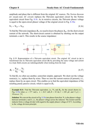
![Exercise 8.7: Three impedances j5Ω, 10Ω, 10Ω are combined in parallel. What is the
equivalent impedance?
Answer: 2:5 þ j2:5 Ω.
Exercise 8.8: In Fig. 8.18, the impedance of the capacitor changes toÀj10Ω. What will be
the phasor current, I, through the capacitor?
Answer: I ¼ 1∠90
A½ Š
8.3.4 Thévenin and Norton Equivalent Circuits
The The´venin’s theorem for steady-state AC circuits is formulated as follows. Any linear
AC network of resistors/capacitors/inductors and voltage/current power sources operat-
ing at the same frequency can be represented in the form of a Thévenin
equivalent network shown in Fig. 8.19b (phasor form). This result is a direct extension
of Thévenin’s theorem for DC circuits stated in Chapter 4. Thévenin’s theorem allows us
to reduce complicated AC circuits to a simple source and the impedance configuration,
with the same power output to a load. The AC frequency remains the same. Phasor
voltage VT is known as The´venin voltage or simply the source voltage; impedance ZT is
called The´venin impedance or source impedance. The phasor voltage may have
10
I
V1
+
-
j10
10 - 5j[A]90
Fig. 8.18. Source transformation applied to the AC circuit from the previous figure.
+
-
10
V1
+
-
j10
10 - 5j[V]9010
Fig. 8.17. An AC circuit solved with the help of source transformation. Note that every impedance
box has a physical counterpart shown within this box.
Chapter 8 Section 8.3: Principles of AC Circuit Analysis
VIII-415](https://image.slidesharecdn.com/practicalelectricalengineering-160720234734/85/Practical-electrical-engineering-429-320.jpg)
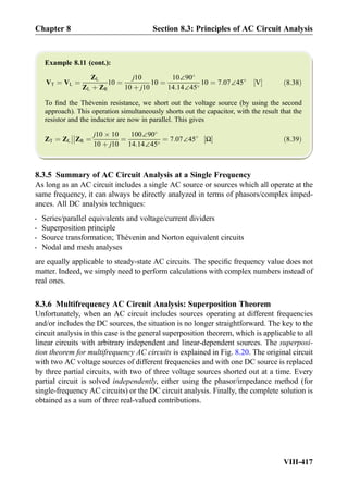
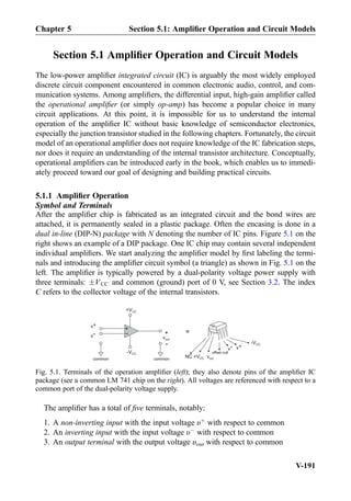
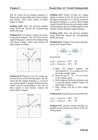
![Summary
Term Meaning/Figure
Steady-state AC
voltage (steady-state
alternating current)
υ tð Þ ¼ Vm cos ωt þ φð Þ
Vm 0 is the voltage
amplitude [V]
ω ¼ 2πf 0 is the angular
frequency [rad/s]
f 0 is the frequency [Hz]
T ¼ 1=f 0 is the period [s]
Àπ φ π is the phase
[rad] or [deg]
Leading/lagging
Euler’s identity e jα
¼ cos α þ j sin α, e jπ=2
¼ j, eÀjπ=2
¼ Àj
Time-domain
signal υ(t) versus
its phasor V; phasor
diagram
Complex phasors
and impedances
ZR ¼ R
ZC ¼
1
jωC
ZL ¼ jωL
(continued)
Chapter 8 Summary
VIII-419](https://image.slidesharecdn.com/practicalelectricalengineering-160720234734/85/Practical-electrical-engineering-433-320.jpg)
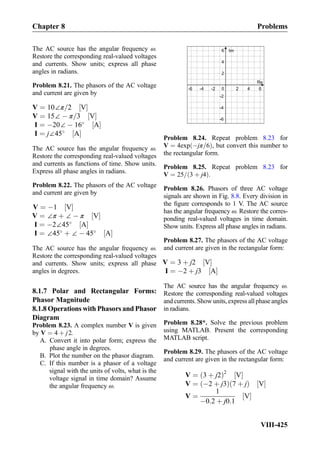
![Problem 8.46. Phasor voltages and currents
for three unknown circuit elements are shown
in the figure below. Determine the type of
the element (R, L, or C) and the value of R,
L, or C.
0 1
I
V
2
1
2
3
a)
0 1
I
V
2
1
2
3
b)
=1000 rad/sec
=3000 rad/sec
0 1
I
V
2
1
2
3
c) =20000 rad/sec
Re (V or A)
Im (V or A)
Re (V or A)
Im (V or A)
Re (V or A)
Im (V or A)
Problem 8.47. Phasor voltages and phasor cur-
rents for three unknown circuit elements are
shown in the figure below. Determine the type of
the element (R, L, or C) and the value of R, L, or
C when appropriate.
0
Re (V or A)
1I
V
2
1
2
3
a)
0 1
I
V
2
1
2
3
b)
=1000 rad/sec
=3000 rad/sec
0 1I V2
1
2
3
c) =20000 rad/sec
Im (V or A)
Re (V or A)
Im (V or A)
Re (V or A)
Im (V or A)
Problem 8.48*. The following MATLAB
script plots the real-valued signals in
time domain corresponding to the phasor
voltage V ¼ 5∠30
V½ Š and to the phasor
current I ¼ 2∠ À 60
A½ Š for an inductor.
clear all
f ¼ 2e6; % frequency, Hz
T ¼ 1/f; % period, sec
dt ¼ T/100; % sampling int.
t ¼ [0:dt:2.5*T]; % time vector
vL ¼ 5*cos(2*pi*f*t+pi/6); % voltage
iL ¼ 2*cos(2*pi*f*t-pi/3); % current
t ¼ t/T; % time in periods
Chapter 8 Problems
VIII-429](https://image.slidesharecdn.com/practicalelectricalengineering-160720234734/85/Practical-electrical-engineering-443-320.jpg)
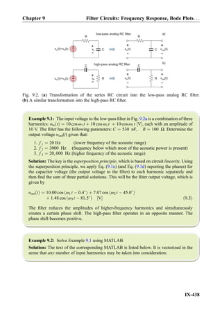
![Example 9.2 (cont.):
Vm = [10 10 10]; % input voltage amplitudes, V
f = [20 3000 20000]; % input voltage frequencies, Hz
omega = 2*pi*f; % angular frequencies, rad/sec
R = 100; % resistance, Ohm
C = 530e-9; % capacitance, F
tau = R*C;
VmC = 1./sqrt(1+(omega*tau).^2).*Vm % output voltage ampl., V
phiC = - atan(omega*tau)*180/pi % output phases in deg
Exercise 9.1: The input voltage to a high-pass filter circuit is a combination of two
harmonics, υin tð Þ ¼ 2 cos ω1 t þ 2 cos ω2 t, with the amplitude of 2 V each. The filter has
the following parameters: R ¼ 100 kΩ and C ¼ 1:59 nF. Determine the output voltage
υout(t) to the filter given that f 1 ¼ 100 Hz and f 2 ¼ 100 kHz.
Answer: υout tð Þ ¼ 1:99 cos ω1 t À 5:7
ð Þ þ 0:02 cos ω2 t À 89:4
ð Þ V½ Š.
Application Example: Effect of a Load Connected to the Filter
The initial excitement about the simplicity of the theoretical filter model often fades
quickly once we try to construct the filter circuit of Fig. 9.2a or Fig. 9.2b in the laboratory.
And the circuit does not work. The major reason for this is the effect of a load connected
to the filter. We consider the low-pass filter in Fig. 9.3.
To solve the circuit with the load, we need to apply the phasor method. The input
voltage is now divided between the resistance R and the parallel combination of the
capacitor impedance and the load resistance, RL. Instead of Eq. (9.1c), we will have
VC ¼
1
ffiffiffiffiffiffiffiffiffiffiffiffiffiffiffiffiffiffiffiffiffiffiffiffiffiffiffiffiffiffiffiffiffiffiffiffiffiffiffiffiffi
1 þ R=RLð Þ2
þ ωτð Þ2
q Vm∠φC V½ Š, φC ¼ À tan À1 ωτ
1 þ R=RL
ð9:4Þ
The proof of this result is suggested in Problems 9.5 and 9.6. The necessary condition for
proper filter operation (both high pass or low pass) is that the filter termination resistance
R
C
+
-
v (t)outv (t)in
+
-
Load
Fig. 9.3. A generic load connected to the low-pass RC filter.
Chapter 9 Section 9.1: First-Order Filter Circuits and Their Combinations
IX-439](https://image.slidesharecdn.com/practicalelectricalengineering-160720234734/85/Practical-electrical-engineering-453-320.jpg)
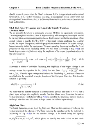
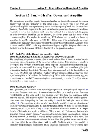
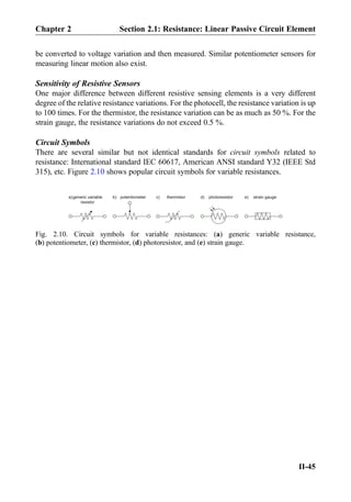
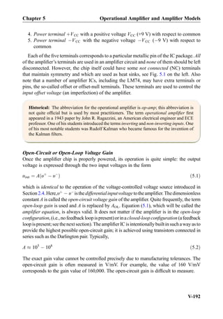
![frequency excites internal resonances, similar to a mechanical mass-spring system, that
continue ad infinitum.
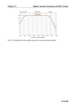
9.2.2 Unity-Gain Bandwidth Versus Gain-Bandwidth Product
The amplifier gain in Fig. 9.11 decreases by a factor of 0.1 (or 20 dB) gain roll-off per
frequency decade. The decay already starts at a relatively low break frequency of 10 Hz
where the DC open-loop gain drops by the factor of 0.707 or 1=
ffiffiffi
2
p
. The corresponding
value in dB is 20log101=
ffiffiffi
2
p
¼ À3 dB. The gain continues to decrease further and
reaches unity at the frequency of 1 MHz. This frequency is equal to the unity-gain
bandwidth (BW) of the amplifier, i.e., for the amplifier IC depicted in Fig. 9.11:
BW ¼ 1 MHz ð9:12Þ
A remarkable observation from Fig. 9.11 is that the gain-bandwidth product (sometimes
denoted by GBWor GB in datasheets) remains constant over the band for every particular
gain value. The gain-bandwidth product is equal to the length of every single arrow
(in Hz) in Fig. 9.11 times the corresponding gain value (dimensionless), that is,
f ¼ 102
Hz ) GBW ¼ 102
 104
¼ 106
Hz ¼ BW,
f ¼ 103
Hz ) GBW ¼ 103
 103
¼ 106
Hz ¼ BW,
f ¼ 104
Hz ) GBW ¼ 104
 102
¼ 106
Hz ¼ BW;
ð9:13Þ
etc. Thus, the gain-bandwidth product is exactly equal to the unity-gain bandwidth BW;
it is frequently specified in the manufacturer datasheet. In what follows, we will use the
unity-gain bandwidth as the major parameter of interest. Note that instead of, or along
Open-loopgain,AOL
105
104
103
102
101
1
106
1 102
103
101
104
105
106
107
Frequency of input voltage, Hz
Open-loopgain[dB],20log10
(AOL)
100
80
60
40
120
20
0
3dB or 0.707A (0)OL
20 dB per decade
roll-off
BWfb
Fig. 9.11. Bode plot of the open-loop gain magnitude for the LM741-type amplifier IC. Note the
logarithmic scale on the left and the corresponding scale in dB on the right. The frequency
bandwidth given by the break frequency fb is only 10 Hz.
Chapter 9 Filter Circuits: Frequency Response, Bode Plots. . .
IX-452](https://image.slidesharecdn.com/practicalelectricalengineering-160720234734/85/Practical-electrical-engineering-466-320.jpg)
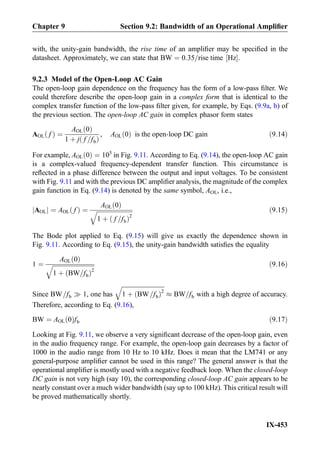
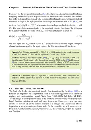
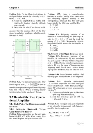
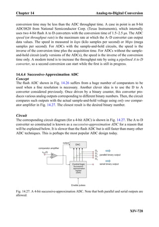
![Example 9.11: An inverting amplifier with a gain of À20 and bandwidth of at least
20 kHz is needed. Is the LM348 chip appropriate for this purpose?
Solution: From the LM348 datasheet, we obtain BW ¼ 1 MHz. Because the inverting
gain is À20, we should use a ratio of R2=R1 ¼ 20. According to Eq. (9.22), this gives
f closed loop
b ¼ 47:6 kHz. The closed-loop 3-dB bandwidth of the amplifier coincides with
this value. Therefore, the LM348 chip is sufficient for our purposes. However, if its gain is
forced to a higher value, say to 100, then the useful bandwidth reduces to 10 kHz.
Exercise 9.7: A non-inverting amplifier with a gain of 31 and a bandwidth of at least
90 kHz is needed. Is an LM741-based amplifier IC appropriate for this circuit?
Answer: No.
10
5
10
4
10
3
10
2
10
1
1
10
6
1 10
2
10
3
10
1
10
4
10
5
10
6
10
7
Frequency of input voltage, Hz
Open-loopgainvs.closed-loopgain[dB]
100
80
60
40
120
20
0
20 dB per decade
roll-off
fb
3dB or 0.707G
Open-loopgainvs.closed-loopgain
3dB or 0.707A (0)OL
open-loop gain
closed-loop gain
closed-loop bandwidth
fb
closed loop
a)
b)
Fig. 9.13. Closed-loop AC gain ACL( f ) (lower curve) versus open-loop AC gain AOL( f ) (upper
curve) for an inverting amplifier with AOL 0ð Þ ¼ 105
and 1 þ R2=R1 ¼ 10 (the amplifier DC gain
is À9).
Chapter 9 Section 9.2: Bandwidth of an Operational Amplifier
IX-457](https://image.slidesharecdn.com/practicalelectricalengineering-160720234734/85/Practical-electrical-engineering-471-320.jpg)
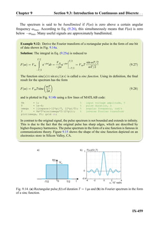
![f tnð Þ ¼
1
NΔT
XNÀ1
m¼0
e j
2π
N mnF ωmð Þ, n ¼ 0, . . . , N À 1 ð9:33Þ
Definition of Discrete Fourier Transform
It is rather inconvenient to keep the factor ΔT in both Eqs. (9.32) and (9.33), respectively.
Therefore, we may introduce the notation
f n½ Š ΔTf tnð Þ, F m½ Š F ωmð Þ ð9:34Þ
and obtain the standard form of the discrete Fourier transform
F m½ Š ¼
XNÀ1
n¼0
eÀj
2π
N mnf n½ Š, m ¼ 0, . . . , N À 1 ð9:35aÞ
f n½ Š ¼
1
N
XNÀ1
m¼0
e j
2π
N mnF m½ Š, n ¼ 0, . . . , N À 1 ð9:35bÞ
Here, f [n] may be treated as an impulse having the area of ΔTf(tn).
Exercise 9.10: Establish a relation betweenF N À m½ Šand F[m] for a real signal f(t), which
is called a reversal property of the discrete Fourier transform.
Answer:
F*
N À m½ Š ¼ F m½ Š ð9:36Þ
where the star again denotes complex conjugate.
Example 9.13: It is possible to very significantly minimize the actual number of multi-
plications necessary to compute a given DFT in Eqs. (9.35a, b). The DFT so constructed is
the fast Fourier transform (FFT) and inverse fast Fourier transform (IFFT). It works best
when N is a power of two. For a pulse f tð Þ ¼ exp À2 t À 5ð Þ2
, 0 s t 10 s, compute
its FFT and then the IFFT and finally compare the end result with the original pulse form
given that N ¼ 64.
Solution: The solution is conveniently programmed using a few lines of a self-explanatory
MATLAB code, which uses Eq. (9.29) and plots two final curves:
Chapter 9 Filter Circuits: Frequency Response, Bode Plots. . .
IX-462](https://image.slidesharecdn.com/practicalelectricalengineering-160720234734/85/Practical-electrical-engineering-476-320.jpg)
![Example 9.13 (cont.):
T = 10; N = 64;
dT = T/N; t = dT*(0:N-1);
f0 = exp(-2*(t-5).^2);
F = fft(f0); f = ifft(F);
plot(t, f, t, f0, '*');
Both curves are virtually identical: the relative integral error (integral of signal difference
magnitude over the integral of signal magnitude) does not exceed 10À16
.
Structure of Discrete Fourier Spectrum
The set of spectrum values F[m], m ¼ 0, . . . , N À 1, of the DFT has an important
redundancy property illustrated in the following example.
Example 9.14: Express all discrete Fourier spectrum values F[m] present in Eq. (9.35a)
through N/2 first values of F[m] only. Hint: Use Eq. (9.36).
Solution:
F 0½ Š, F 1½ Š, . . . , F
N
2
À 1
!
, F
N
2
!
, F
N
2
þ 1
!
, . . . , F N À 1½ Š ¼
F 0½ Š, F 1½ Š, . . . , F
N
2
À 1
!
, F
N
2
!
, F* N
2
À 1
!
, . . . , F*
1½ Š
ð9:37Þ
Equation (9.37) demonstrates how the output of the DFT (and of the FFT, in particular in
MATLAB) is arranged in reality. It is a symmetric conjugate aboutm ¼ N=2. Equation (9.37)
is a key to finding derivatives and arbitrary filter transformations of the input signal with the
FFT. Only a frequency with m N=2 is considered to be valid; its mirror reflection about
m ¼ N=2 is a higher “aliasing frequency.” We emphasize that, according to Eq. (9.26), the
complex conjugates may be replaced by spectrum values at a negative frequency, i.e.,
F*
1½ Š ¼ F À1½ Š. Thus, the spectrum above m ¼ N=2 corresponds to negative frequencies
with m ÀN=2.
9.3.4 Sampling Theorem
It follows from Example 9.14 that only frequency samples with ωm
N
2 ω0 are really
needed. This fact is a consequence of the sampling theorem, which states that any signal
bandlimited to ωmax can be reproduced exactly using the discrete Fourier transform if
ωmax
N
2
ω0 ð9:38aÞ
Chapter 9 Section 9.3: Introduction to Continuous and Discrete. . .
IX-463](https://image.slidesharecdn.com/practicalelectricalengineering-160720234734/85/Practical-electrical-engineering-477-320.jpg)
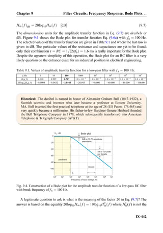
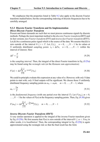
![Example 9.15 (numerical differentiation via the FFT) (cont.):
T = 10; N = 64;
dT = T/N; t = dT*(0:N-1);
f = exp(-2*(t-5).^2); % input pulse
omega = (2*pi/T)*[0:N/2]; % non-aliasing frequencies
H = j*omega; % H at non-aliasing frequencies
F = fft(f); % FFT spectrum
HF = F.*[H, conj(H(end-1:-1:2))]; % HF according to Eq. (9.40)
fder = real(ifft(HF)); % numerical derivative
fder0 = -4*(t-5).*f; % analytical derivative
plot(t, fder0, t, fder, 'd'); % compare both derivatives
Both curves are virtually identical: the relative integral error (integral of signal difference
magnitude over the integral of analytical signal magnitude) does not exceed 1.3 Â 10À15
.
9.3.7 Application Example: Filter Operation for an Input Pulse Signal
The filter operation for an input pulse signal exactly follows Example 9.15 but with a
different transfer function H(ω).
Example 9.16: A pulse f tð Þ ¼ exp À2 t À 5ð Þ2
, 0 s t 10 s is an input to a first-
order high-pass filter. Find the filter output when its (angular) break frequency is given by
a) ω0 ¼ 1 rad=s and b) ω0 ¼ 10 rad=s. Use the FFT and IFFT with N ¼ 64.
Solution: The solution is performed and programmed exactly described in the previous
example, but the transfer function is now given by Eq. (9.1b):
H ¼ j*omega/omega0./(1+j*omega/omega0);
t, s 10
-1.5
-1
-0.5
0
0.5
1
1.5
df(t)/dt
0 5
Fig. 9.16. Analytical (solid curve) and numerical (diamonds) differentiation of the original
Gaussian pulse.
Chapter 9 Filter Circuits: Frequency Response, Bode Plots. . .
IX-466](https://image.slidesharecdn.com/practicalelectricalengineering-160720234734/85/Practical-electrical-engineering-480-320.jpg)
![Summary
Property First-order low-pass filter First-order high-pass filter
Circuit schematic
Transmission at
f ¼ 0 (DC)
1
(DC path through the resistor)
0
(No DC path)
Transmission at
f ! 1
0
(Inductor is an open circuit
at f ! 1)
1
(DC path through the resistor)
Transfer function
H( f )
1
1 þ j f =f bð Þ
f =f bð Þ
1 þ j f =f bð Þ
Decibels of H ¼ Hj j 20 log10H [dB] 20 log10H [dB]
Decibels of 1 and 0.1 0 dB and À20 dB 0 dB and À20 dB
Transfer function
magnitude Hm( f )
1
ffiffiffiffiffiffiffiffiffiffiffiffiffiffiffiffiffiffiffiffiffiffiffiffiffi
1 þ f =f bð Þ2
q
f =f b
ffiffiffiffiffiffiffiffiffiffiffiffiffiffiffiffiffiffiffiffiffiffiffiffiffi
1 þ f =f bð Þ2
q
Transfer function
phase ∠φH
∠ À tan À1 f
f b
π
2
À tan À1 f
f b
Break frequency,
(half-power fre-
quency, 3-dB
frequency, corner
frequency)
f b ¼
1
2πτ
Hz½ Š
τ ¼ RC or
L
R
s½ Š
f b ¼
1
2πτ
Hz½ Š
τ ¼ RC or
L
R
s½ Š
Passband (3 dB
bandwidth), Hz
From 0 to fb From fb to 1
Filter with a resistive
load RL
(continued)
Chapter 9 Summary
IX-469](https://image.slidesharecdn.com/practicalelectricalengineering-160720234734/85/Practical-electrical-engineering-483-320.jpg)
![Problems
9.1 First-Order Filter
Circuits and Their
Combinations
9.1.1 RC Voltage Divider as an Analog
Filter
Problem 9.1
A. Explain the function of an analog RC
filter.
B. Write the capacitor and resistor voltages
υR(t) and υC(t) of the series RC circuits
in the general form, as functions of the
AC angular frequency.
C. Which circuit element (or which voltage)
dominates at low frequencies? At high
frequencies?
Problem 9.2
A. Draw a schematic of the low-pass analog
RC filter. Show the input and output
ports.
B. Repeat the same task for the high-pass
analog RC filter.
Problem 9.3. The input voltage to the filter
circuit shown in the following figure is a com-
bination of two harmonics,
υin tð Þ ¼ 1 cos ω1 t þ 1 cos ω2 t, with the ampli-
tude of 1 V each. The filter has the following
parameters: R ¼ 100 kΩ and C ¼ 1:59 nF.
Determine the output voltage υout(t) to the filter
given that f 1 ¼ 100 Hz and f 2 ¼ 100 kHz.
Express all phase angles in degrees.
R
C
+
-
v (t)outv (t)in
+
-
Problem 9.4. Repeat the previous problem
for the filter circuit shown in the
following figure. All other parameters remain
the same.
C
R
+
-
v (t)in
+
-
v (t)out
Problem 9.5. The input voltage to the RC
filter circuit shown in the figure is
Vin tð Þ ¼ 5 cos ωt V½ Š. The filter has the fol-
lowing parameters: C ¼ 1 μF and
R ¼ 100 Ω. The filter operates in the fre-
quency band from 100 Hz to 50 kHz. The filter
is connected to a load with the load resistance
of 1 MΩ. By solving the corresponding AC
circuit, determine the output voltage amplitude
across the load (and its percentage versus the
input voltage amplitude) with and without the
load at f ¼ 100 Hz, f ¼ 1592 Hz, and
f ¼ 50 kHz.
R
C
+
-
v (t)outv (t)=5cos(wt) [V]in
+
-
Load
Problem 9.6. Repeat the previous problem
when the load resistance changes from 1 MΩ
to 100 Ω (decreases).
Problem 9.7. Repeat Problem 9.5 for the filter
circuit shown in the following figure. Assume
the load resistance of 100 Ω.
R
C
+
-
v (t)outv (t)=5cos( t) [V]in w
+
-
Load
Chapter 9 Problems
IX-473](https://image.slidesharecdn.com/practicalelectricalengineering-160720234734/85/Practical-electrical-engineering-487-320.jpg)
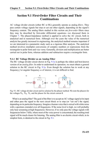
![C. Compute equivalent frequency samples
using negative frequencies.
D. Compute all discrete samples f [n].
E. Compute all discrete samples F[m] using
the definition of the discrete Fourier
transform. Explain the physical meaning
of their values.
F. Repeat the previous step using function
fft of MATLAB. Compare both sets of
F[m].
G. Restore all discrete samples f [n] using
the definition of the inverse discrete Fou-
rier transform. Compare them with the
exact function values.
H. Repeat the previous step using function
ifft of MATLAB. Compare both sets of
f [n].
Problem 9.58. Repeat the previous problem for
the signal f tð Þ ¼ cos t. All other parameters
remain the same.
Problem 9.59. For Problem 9.57, establish and
prove a discrete version of Parseval’s theorem
formulated in Problem 9.55.
Problem 9.60. An input signal to a filter has a
discrete frequency spectrum
F m½ Š, m ¼ 0, . . . , N À 1 computed via the
FFT. You are given filter transfer function
H computed at N
2 þ 1 frequency points of the
FFT, H m½ Š, m ¼ 0, . . . , N=2. Compute the
discrete spectrum of the filter’s output to be
fed into the IFFT.
9.3.6 Application Example: Numerical
Differentiation via the FFT
9.3.7 Application Example: Filter Oper-
ation for an Input Pulse Signal
Problem 9.61*. Present the text of a MATLAB
script that numerically differentiates the input
signal f tð Þ ¼ sin t over the time interval from
0 to 4π s using the FFT with 4096 sampling
points and plot the resulting signal derivative.
Problem 9.62. Repeat the previous problem for
the signal f tð Þ ¼ exp À t À 2πð Þ2
. All other
parameters remain the same.
Problem 9.63. A monopolar pulse
f tð Þ ¼ exp À2 t À 5ð Þ2
, 0 t 10 s is
an input to a series combination of two identical
first-order high-pass filters. Find the output of
the filter combination when the (angular) break
frequency is given by:
A. ω0 ¼ 0:5 rad=s
B. ω0 ¼ 10 rad=s
Use the FFT and IFFT with N ¼ 64. Plot the
filter output and explain the output signal
behavior in every case.
Problem 9.64. A bipolar pulse
f tð Þ ¼ 5Àtð Þexp À2 t À5ð Þ2
, 0 t 10s is
an input to a first-order low-pass filter. Find the
filter output when its (angular) break frequency
is given by:
A. ω0 ¼ 0:5 rad=s
B. ω0 ¼ 5 rad=s
Use the FFT and IFFT with N ¼ 64. Plot the
filter output along with the input signal on the
same graph and explain the output signal
behavior in both cases.
Chapter 9 Filter Circuits: Frequency Response, Bode Plots. . .
IX-480](https://image.slidesharecdn.com/practicalelectricalengineering-160720234734/85/Practical-electrical-engineering-494-320.jpg)
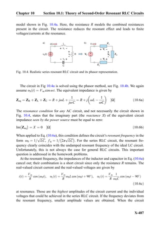
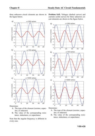
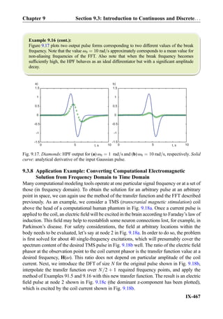
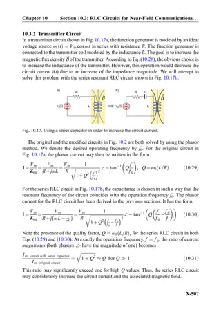
![resistance is small, large circuit current and large capacitor and inductor voltages may be
achieved at the resonance. You have to be aware of the fact that it is not uncommon to
measure voltage amplitudes of 50–500 Vacross the individual elements in the laboratory,
whereas the driving source voltage may only have an amplitude of 10 V. The circuit in
Fig. 10.4 is also called the series RLC tank circuit.
Exercise 10.2: In the series resonant RLC circuit shown in Fig. 10.4, Vm ¼ 10 V,
L ¼ 50 μH, C ¼ 0:5 nF, R ¼ 50 Ω. Determine the real-valued circuit current and the
inductor/capacitor voltages at the resonance.
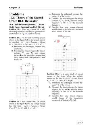
Answer:
i tð Þ ¼ 0:2 cos ωtð Þ A½ Š, υL tð Þ ¼ 63:3 cos ωt þ 90
ð Þ V½ Š,
υC tð Þ ¼ 63:3 cos ωt À 90
ð Þ V½ Š:
ð10:7Þ
Could we increase the resonant voltage amplitudes of the series RLC circuit in
Fig. 10.4a [see Eq. (10.6c)] while keeping the voltage source and the circuit resistance
unaltered? Yes we can. However, one more concept is required for this and similar
problems: the concept of the quality factor of a resonator.
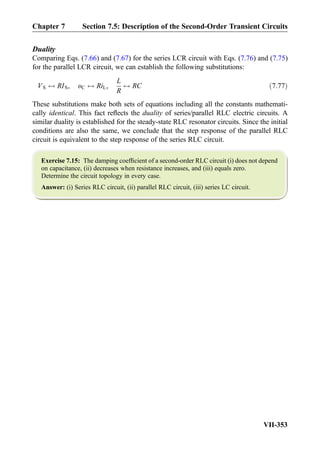
10.1.4 Quality Factor Q of the Series Resonant RLC Circuit
Multiple factors in front of resonant voltages and currents expressions can be reduced to
one single factor. Using the definition of the resonant frequency ω0, Eq. (10.6c) at the
resonance may be rewritten in the simple form
i tð Þ ¼
Vm
R
cos ω0tð Þ, υL tð Þ ¼ QVm cos ω0t þ90
ð Þ, υC tð Þ ¼ QVm cos ω0t À 90
ð Þ
ð10:8Þ
where the dimensionless constant
Q ¼
ffiffiffiffiffiffiffiffi
L=R
p
ffiffiffiffiffiffiffi
RC
p ¼
ffiffiffiffiffiffiffiffiffi
L=C
p
R
ð10:9Þ
is called the quality factor of the series resonant RLC circuit. The equivalent forms are
Q ¼
1
ω0RC
¼ ω0
L
R
ð10:10Þ
Thus, in order to increase the resonant voltage amplitudes in Eq. (10.8), we should simply
increase the quality factor of the resonator. Even if the circuit resistance remains the same,
we can still improve Q by increasing the ratio of L/C in Eq. (10.9). This observation
Chapter 10 Second-Order RLC Circuits
X-488](https://image.slidesharecdn.com/practicalelectricalengineering-160720234734/85/Practical-electrical-engineering-502-320.jpg)
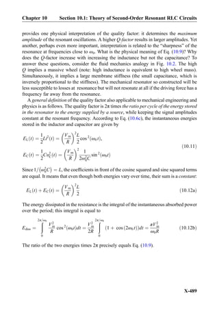
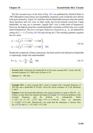
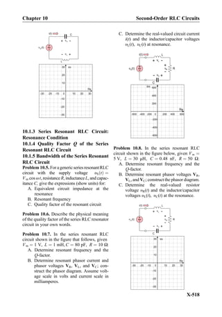
![Example 10.6: Create Bode plots as seen in Fig. 10.5 using MATLAB.
Solution: We create only one bandwidth curve, for Q ¼ 2. Other curves are obtained
similarly, using the command hold on.
f = logspace(3, 5, 101); % frequency vector, Hz(from 10^3 to 10^5 Hz)
f0 = 1e4; % resonant frequency, Hz
Q = 2; % quality factor, dimensionless
H = 1./sqrt(1+Q^2*(f/f0-f0./f).^2);
HdB = 20*log10(H);
semilogx(f, HdB, 'r'); grid on;
title('Bode plot');
xlabel('frequency, Hz'); ylabel('H, dB')
axis([min(f) max(f) -30 0])
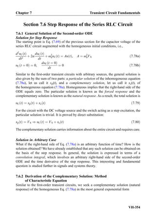
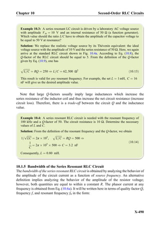
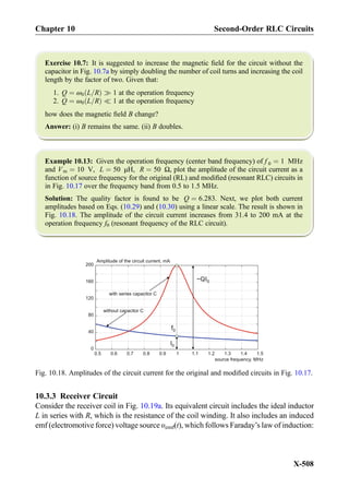
10.1.6 Parallel Resonant RLC Circuit: Duality
The parallel resonant RLC circuit is shown in Fig. 10.6. It is driven by an alternating
current source iS tð Þ ¼ Im cos ωt. The parallel RLC resonator is a current divider circuit,
which is the dual to the series RLC resonator (which is a voltage divider) in Fig. 10.4.
While the series RLC resonator is capable of creating large voltages (or “amplifying” the
supply voltage), the parallel RLC resonator circuit is capable of producing large currents.
The amplitudes of the currents through the inductor and the capacitor may be large, much
larger than the supply current itself. The circuit in Fig. 10.6 is also called the parallel RLC
tank circuit.
The circuit in Fig 10.6a is solved by using the phasor method; see Fig. 10.6b. The
equivalent impedance is given by
1
Zeq
¼
1
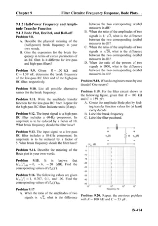
ZR
þ
1
ZL
þ
1
ZC
¼
1
R
þ
1
jωL
þ jωC ¼
1
R
À j
1 À LCω2
ωL
Ω½ Š ð10:18Þ
The resonance condition for any AC circuit states that the impedance Zeq must be a
purely real number at resonance. If the impedance is real, its reciprocal, the admittance, is
also real and vice versa. Therefore, from Eq. (10.18), we obtain the resonant frequency
R
i (t)S
LZ CZIS
V
+
-
b)a)
RZL C
i (t)S
+
-
v
+
-
v
+
-
v
+
-
v
IS
V
+
-V
+
-
Fig. 10.6. Parallel resonant RLC circuit and its phasor representation.
Chapter 10 Section 10.1: Theory of Second-Order Resonant RLC Circuits
X-493](https://image.slidesharecdn.com/practicalelectricalengineering-160720234734/85/Practical-electrical-engineering-507-320.jpg)
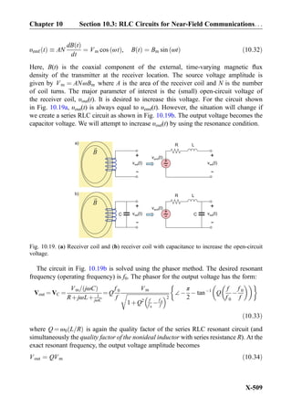
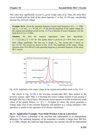
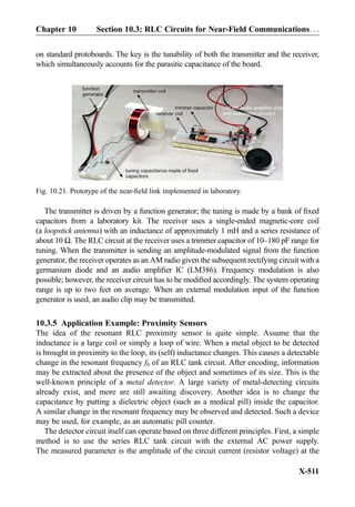
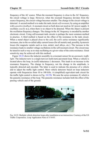


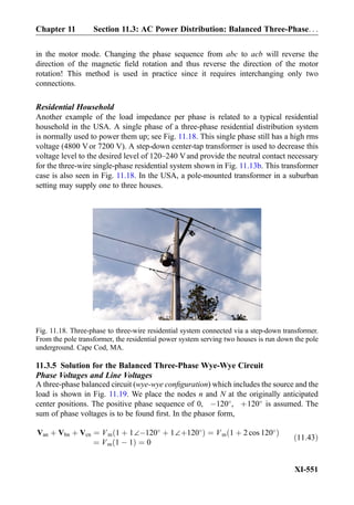


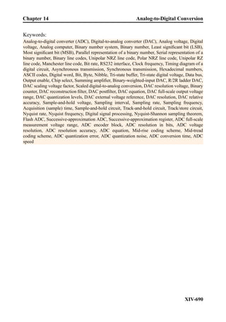


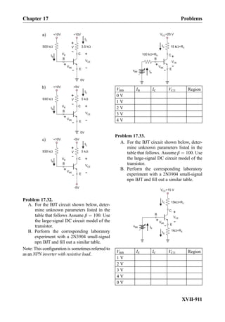


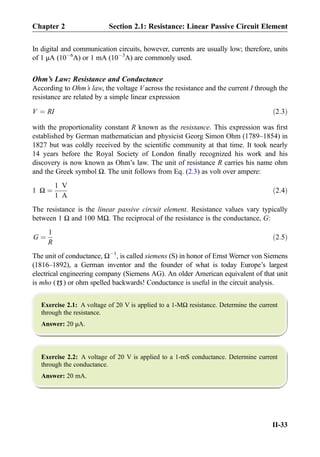
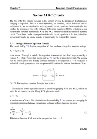
This document provides an overview of the book "Practical Electrical Engineering" by Sergey N. Makarov, Reinhold Ludwig, and Stephen J. Bitar. The book covers topics in electrical engineering including electrostatics, circuit theory, circuit elements, circuit analysis methods, operational amplifiers, and amplifier models. It is intended to provide practical knowledge of electrical engineering concepts for applications. The book contains chapters on major circuit elements, circuit laws and theorems, circuit analysis and power transfer, and operational amplifiers. It also includes examples and analogies to help explain different electrical engineering topics.