This document contains information about WileyPLUS, an online learning environment for teaching and learning. It describes some of the key features of WileyPLUS, including interactive textbooks and resources, assignments, presentations, tutorials, technical and student support, and connections between instructors and students.


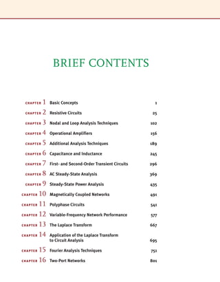


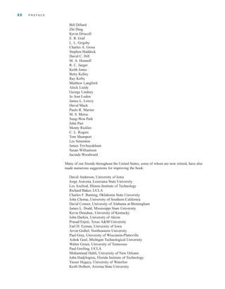


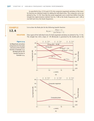
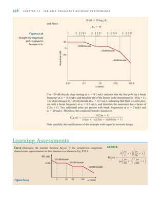
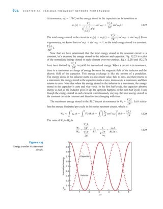
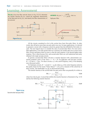
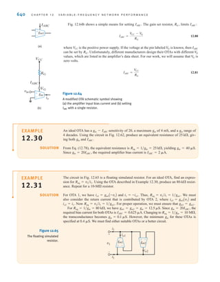
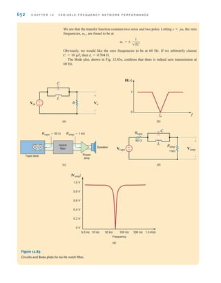
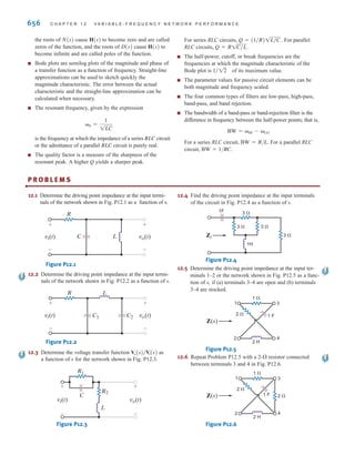
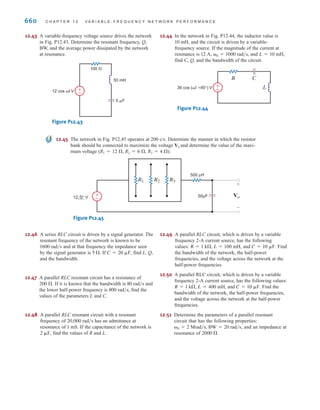
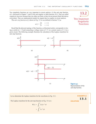
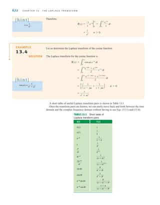
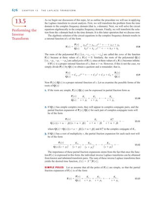
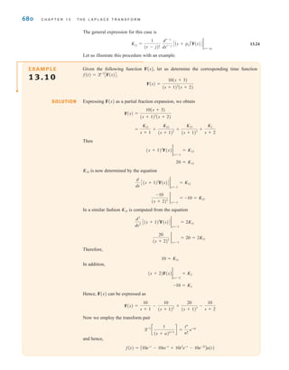
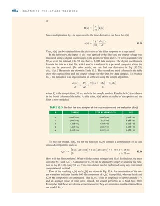
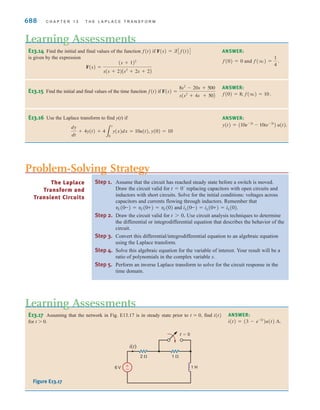
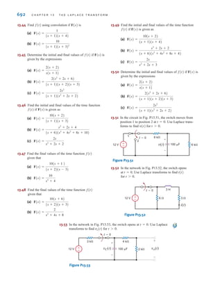
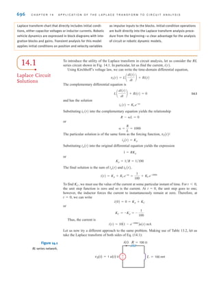
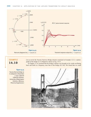
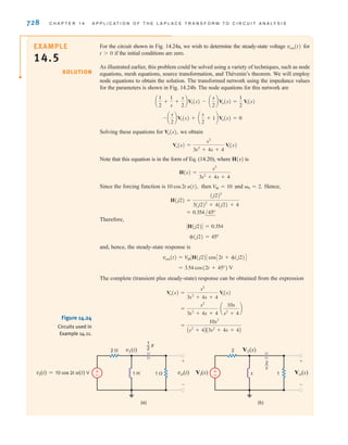
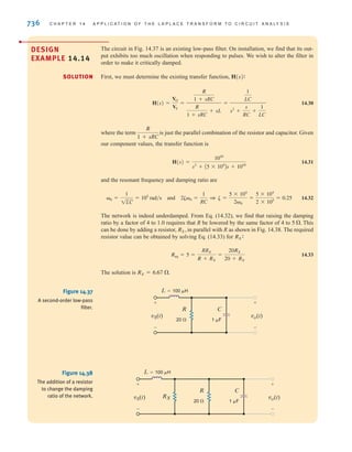
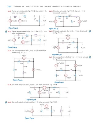
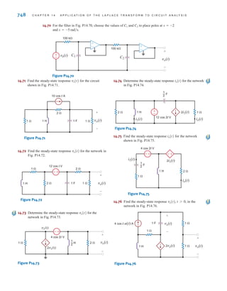
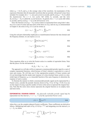
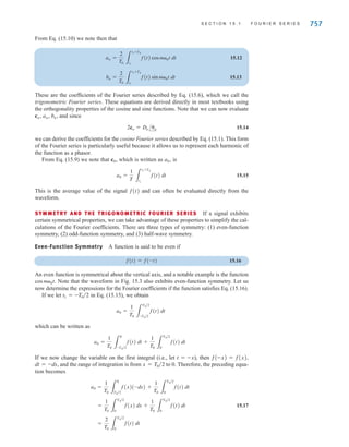
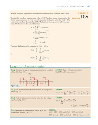
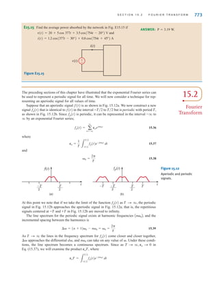
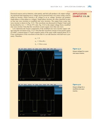
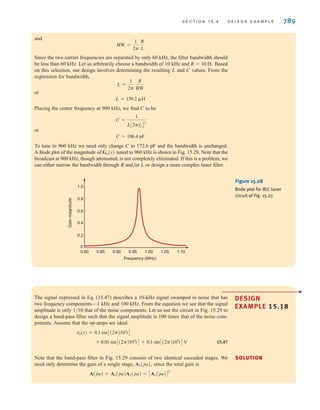
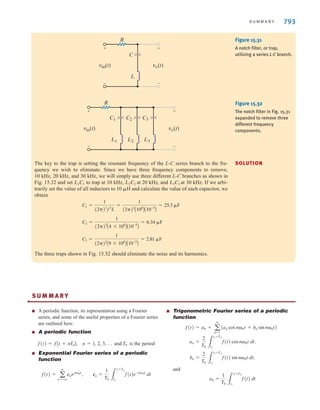
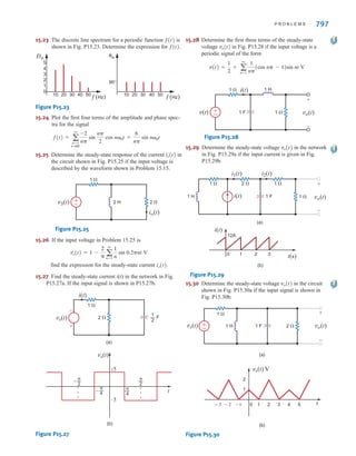
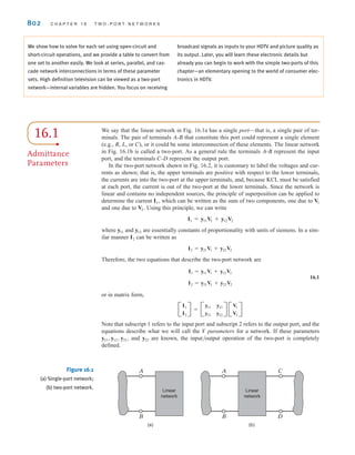
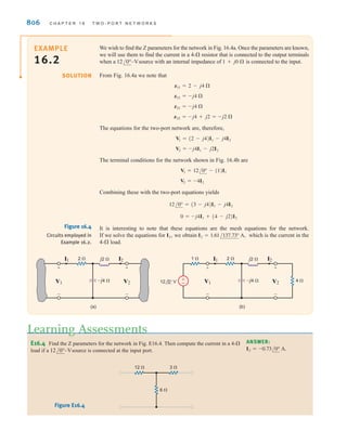
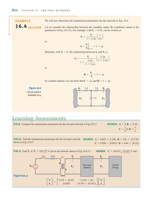
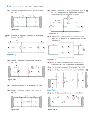
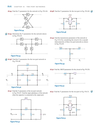
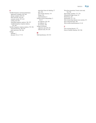
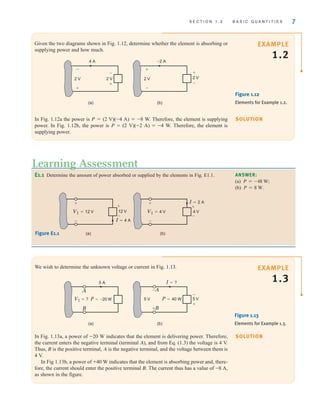
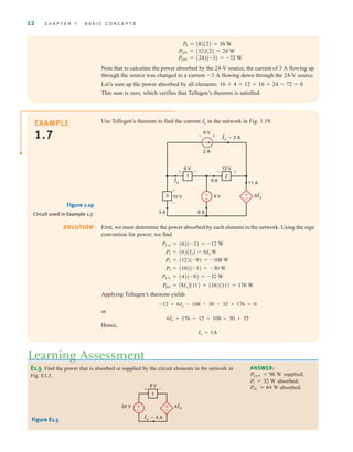
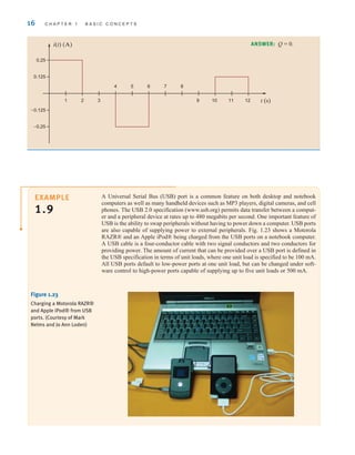
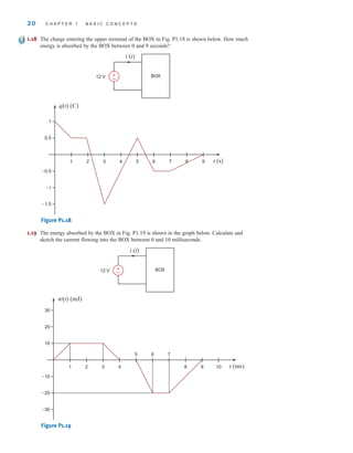
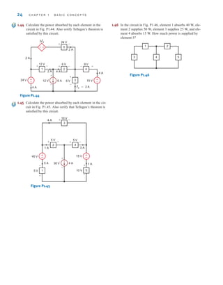
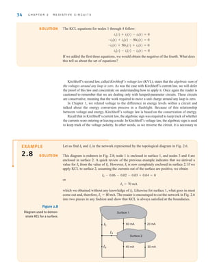
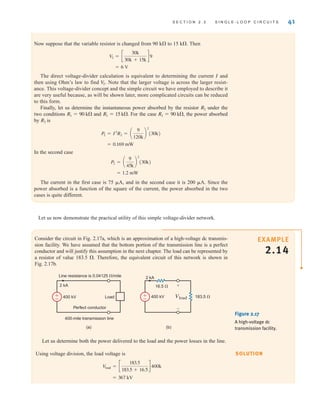
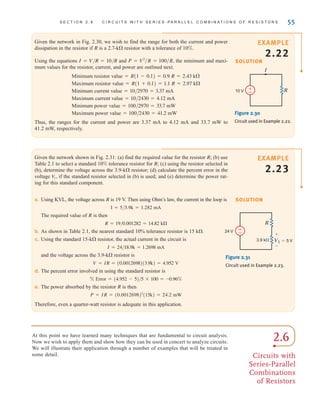
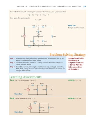
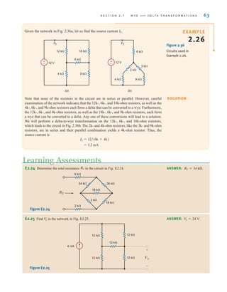
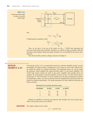
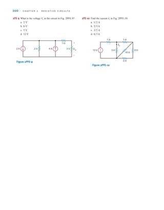
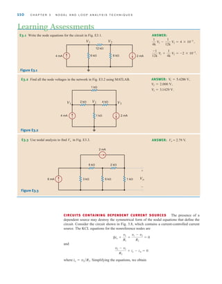
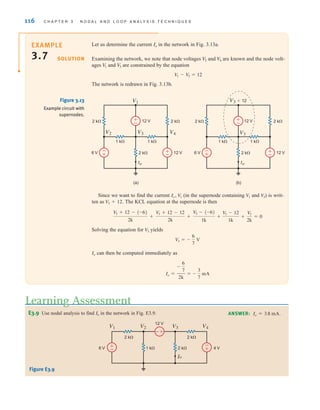
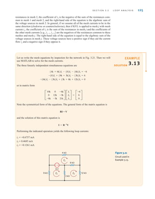
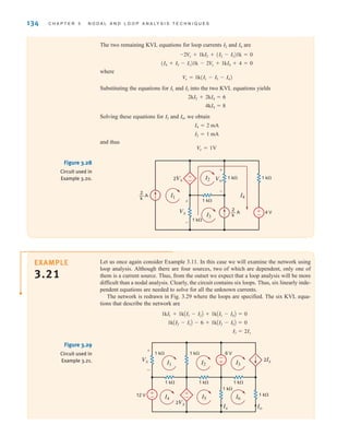
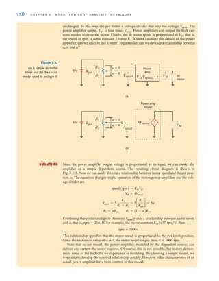
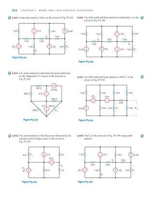
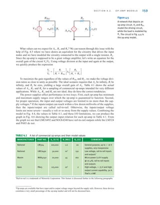
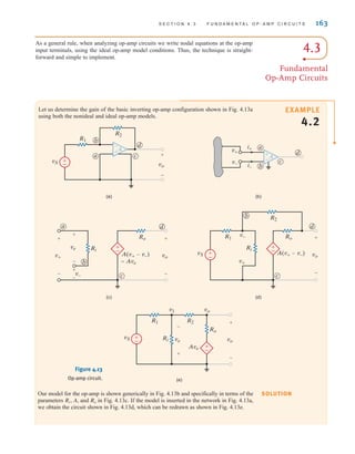
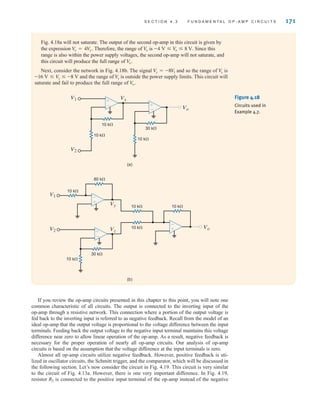
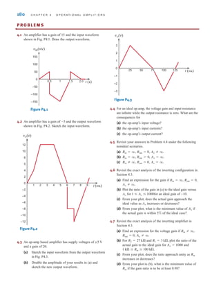
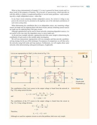
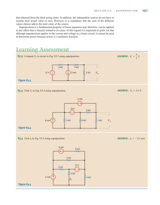
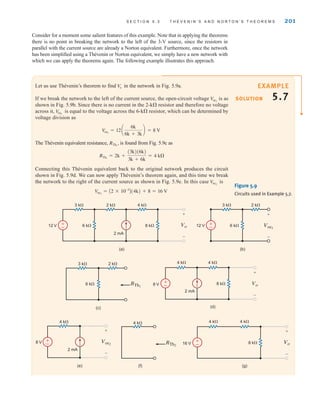
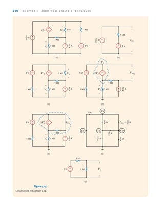
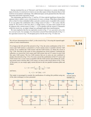
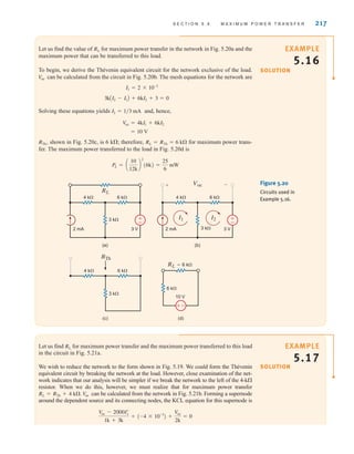
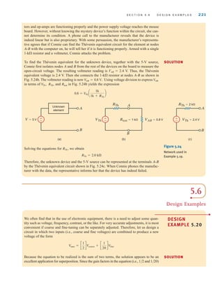
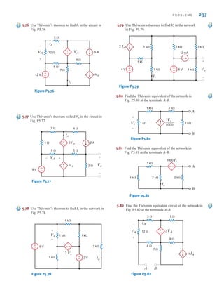
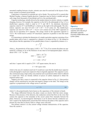
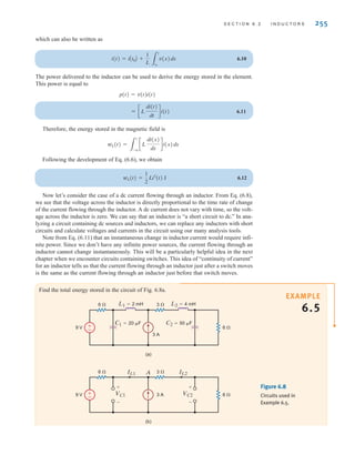
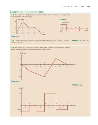
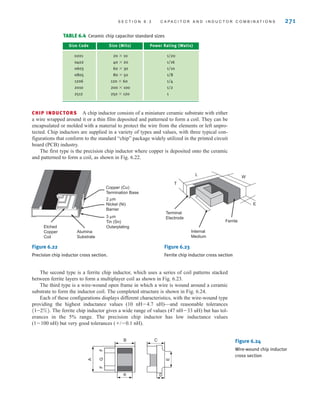
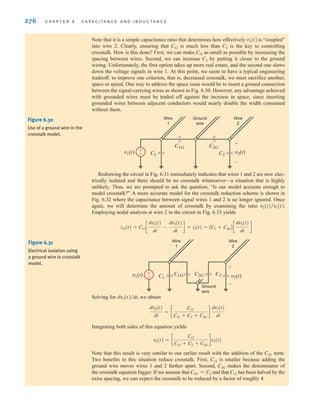
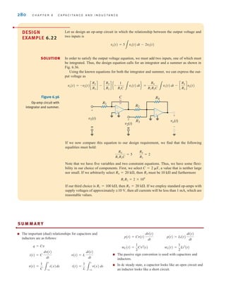
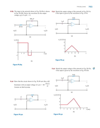
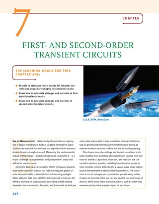
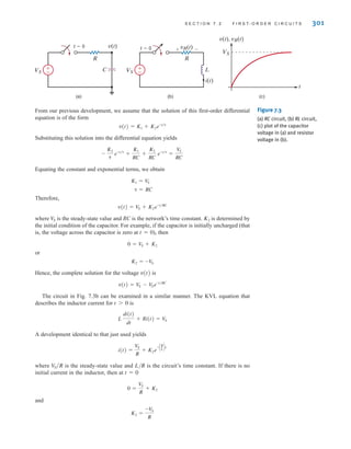
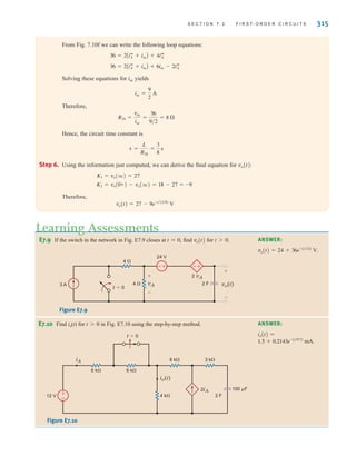
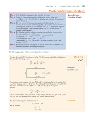
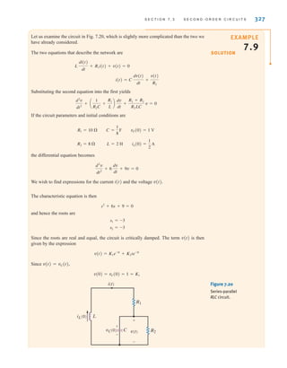
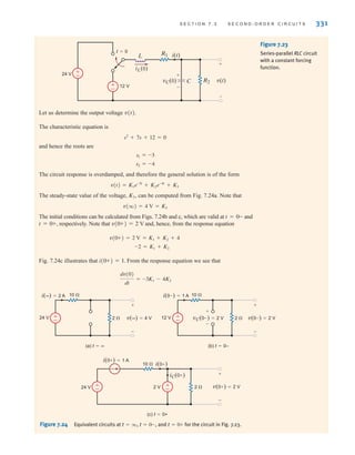
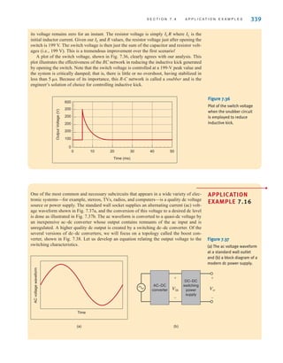
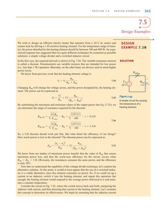
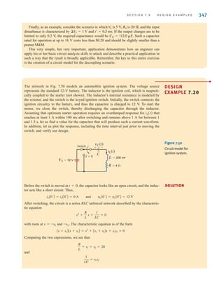
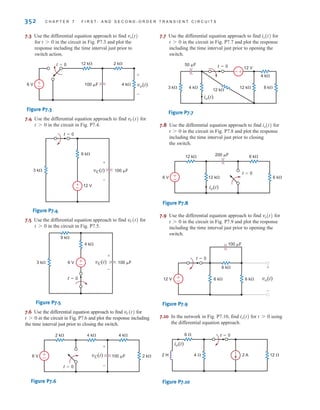
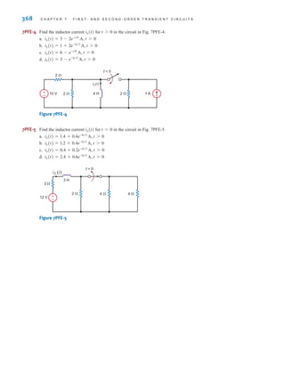
![The two types of current that we encounter often in our daily lives, alternating current (ac)
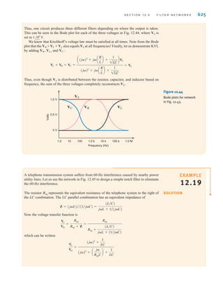
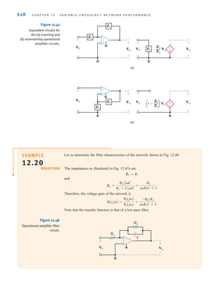
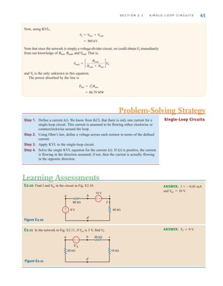
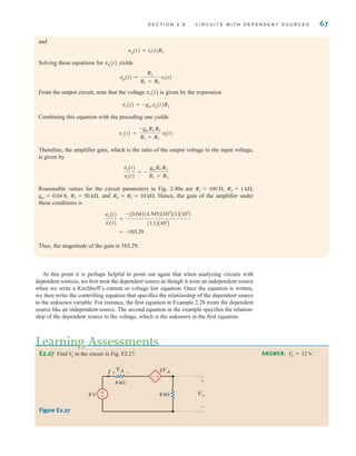
and direct current (dc), are shown as a function of time in Fig. 1.3. Alternating current is the
common current found in every household and is used to run the refrigerator, stove, washing
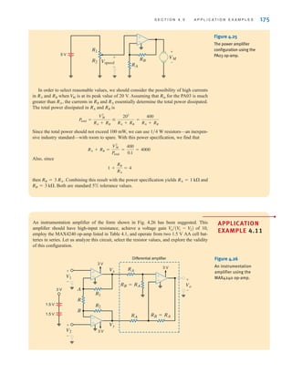
machine, and so on. Batteries, which are used in automobiles and flashlights, are one source
of direct current. In addition to these two types of currents, which have a wide variety of uses,
we can generate many other types of currents. We will examine some of these other types
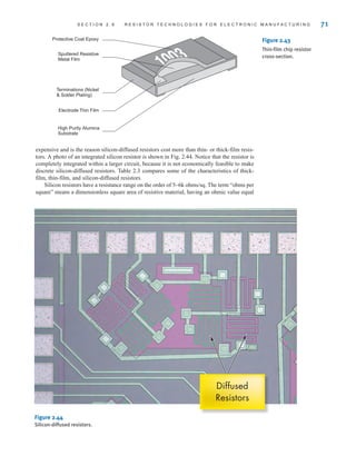
later in the book. In the meantime, it is interesting to note that the magnitude of currents in
elements familiar to us ranges from soup to nuts, as shown in Fig. 1.4.
We have indicated that charges in motion yield an energy transfer. Now we define the
voltage (also called the electromotive force, or potential) between two points in a circuit as the
difference in energy level of a unit charge located at each of the two points. Voltage is very sim-
ilar to a gravitational force. Think about a bowling ball being dropped from a ladder into a tank
of water. As soon as the ball is released, the force of gravity pulls it toward the bottom of the
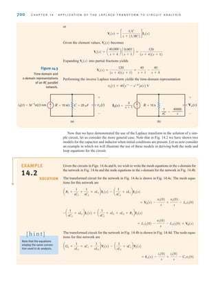
tank. The potential energy of the bowling ball decreases as it approaches the bottom. The grav-
itational force is pushing the bowling ball through the water. Think of the bowling ball as a
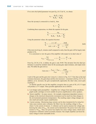
charge and the voltage as the force pushing the charge through a circuit. Charges in motion
represent a current, so the motion of the bowling ball could be thought of as a current. The
water in the tank will resist the motion of the bowling ball. The motion of charges in an elec-
tric circuit will be impeded or resisted as well. We will introduce the concept of resistance in
Chapter 2 to describe this effect.
Work or energy, w(t) or W, is measured in joules (J); 1 joule is 1 newton meter (N⭈m).
Hence, voltage [v(t) or V] is measured in volts (V) and 1 volt is 1 joule per coulomb; that is,
1 volt=1 joule per coulomb=1 newton meter per coulomb. If a unit positive charge is
moved between two points, the energy required to move it is the difference in energy level
between the two points and is the defined voltage. It is extremely important that the variables
used to represent voltage between two points be defined in such a way that the solution will
let us interpret which point is at the higher potential with respect to the other.
S E C T I O N 1 . 2 B A S I C Q U A N T I T I E S 3
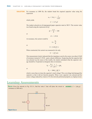
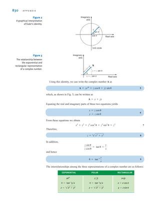
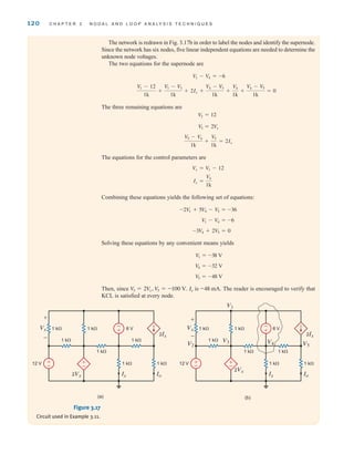
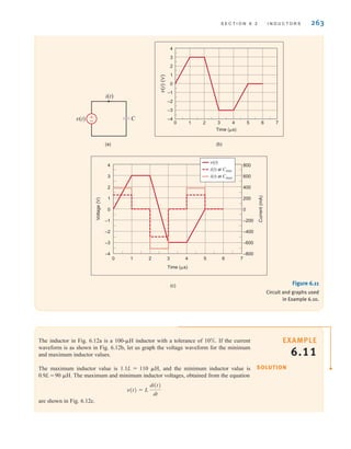
Figure 1.3
Two common types
of current: (a) alternating
current (ac); (b) direct
current (dc).
i(t)
t t
i(t)
(a) (b)
Figure 1.4
Typical current magnitudes.
Lightning bolt
Large industrial motor current
Typical household appliance current
Causes ventricular fibrillation in humans
Human threshold of sensation
Integrated circuit (IC) memory cell current
Synaptic current (brain cell)
106
104
102
100
10–2
10–4
10–6
10–8
10–10
10–12
10–14
Current
in
amperes
(A)
irwin01_001-024hr.qxd 30-06-2010 13:16 Page 3](https://image.slidesharecdn.com/basic-engineering-circuit-analysis-10th-irwin-220801002926-2b111212/85/basic-engineering-circuit-analysis-10th-Irwin-pdf-27-320.jpg)
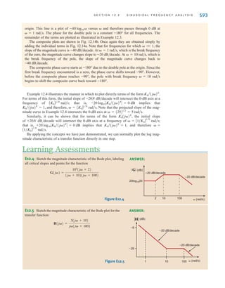
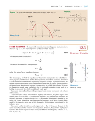
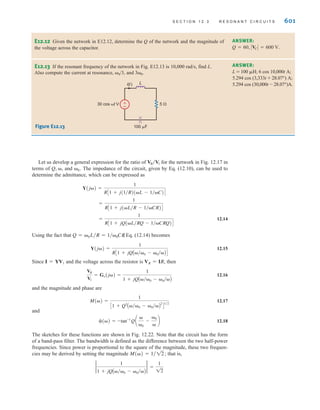
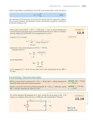
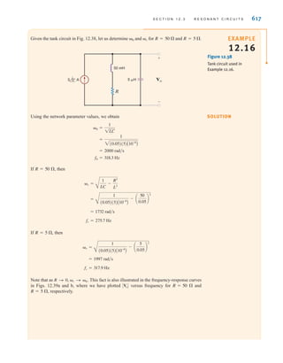
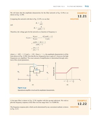
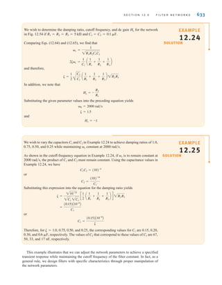
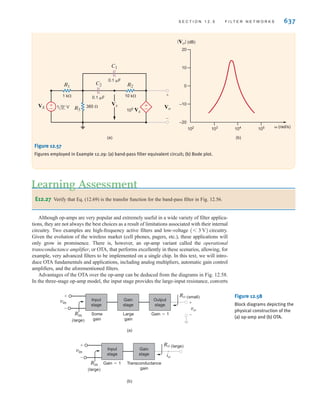
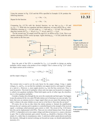
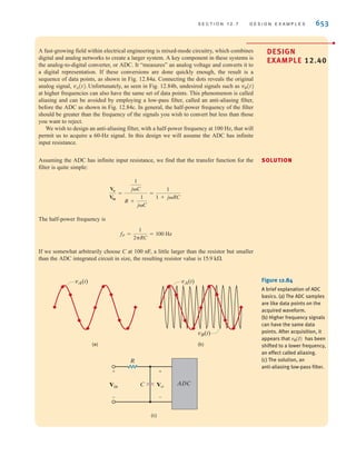
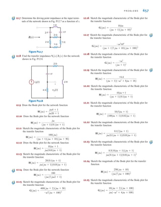
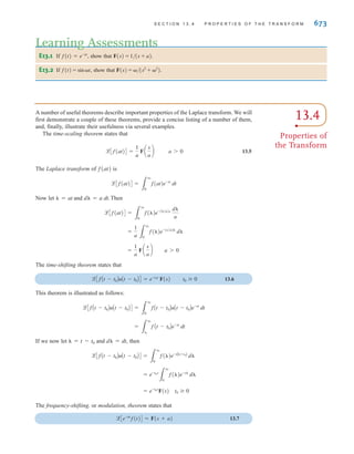
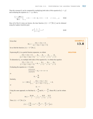
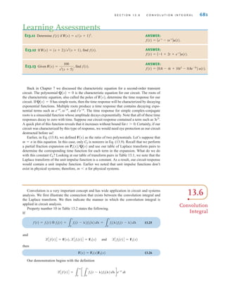
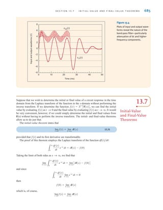
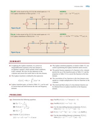
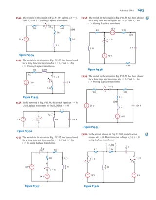
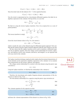
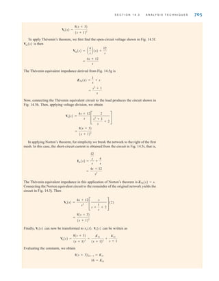
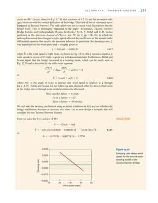
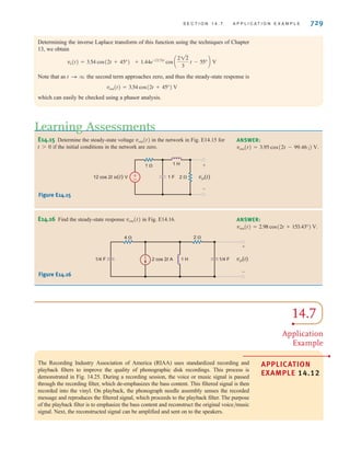
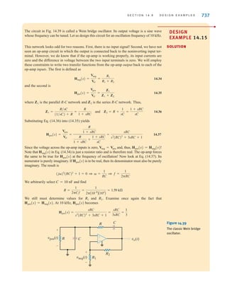
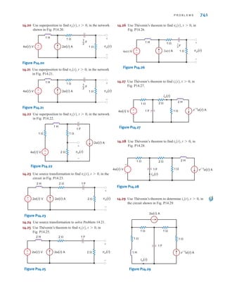
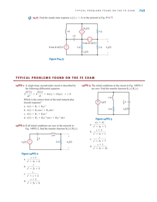
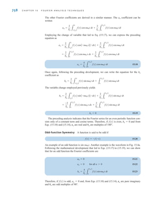
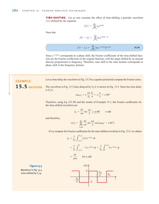
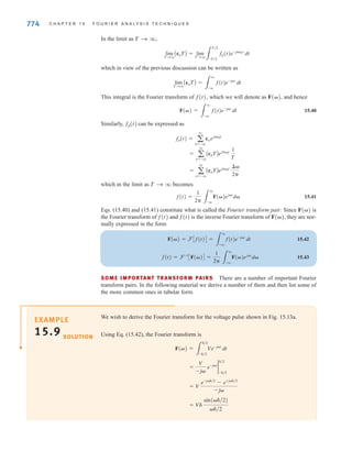
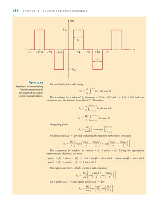
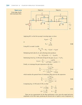
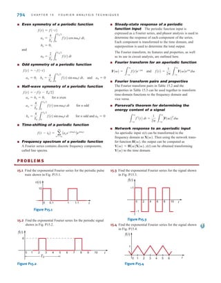
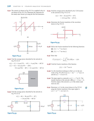
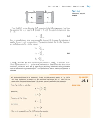
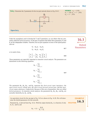
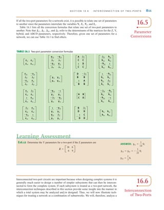
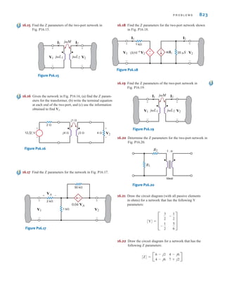
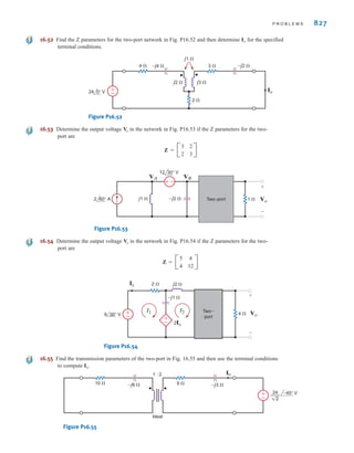
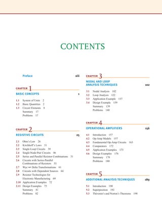
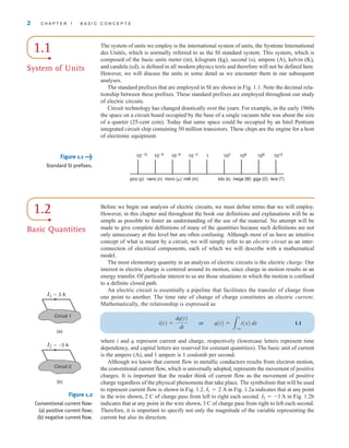
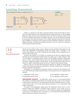
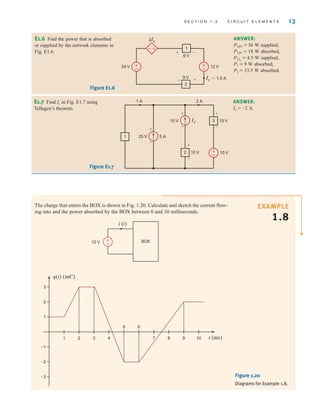
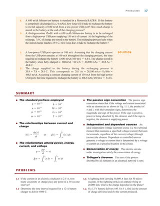
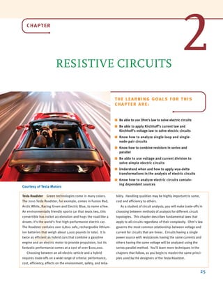
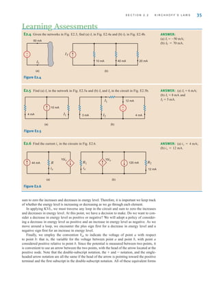
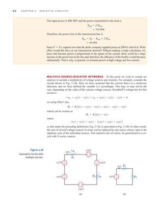
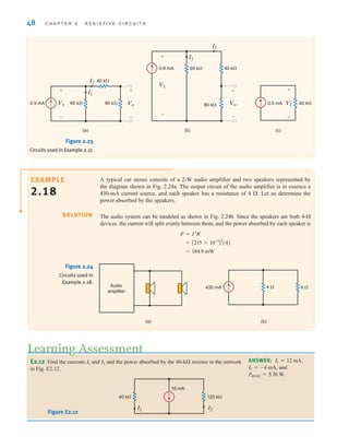
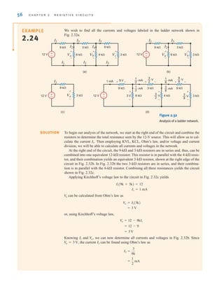
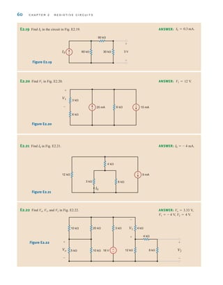
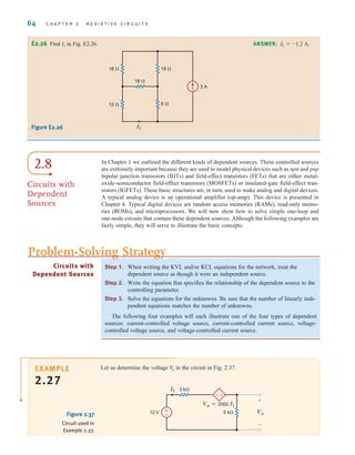
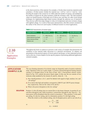
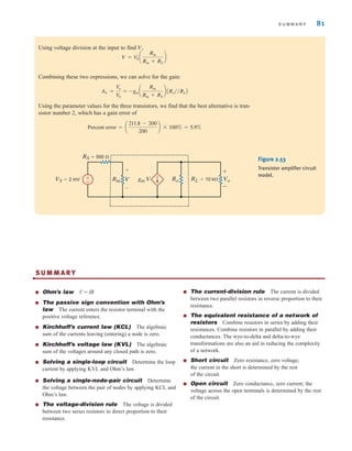
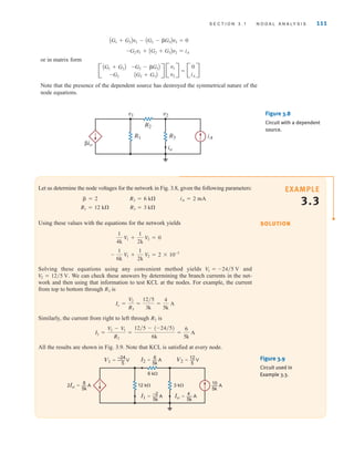
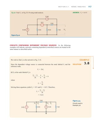
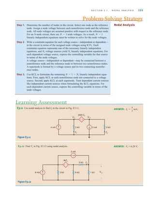
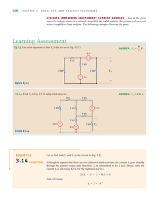
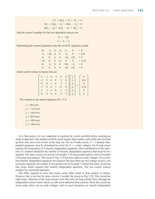
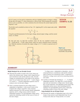
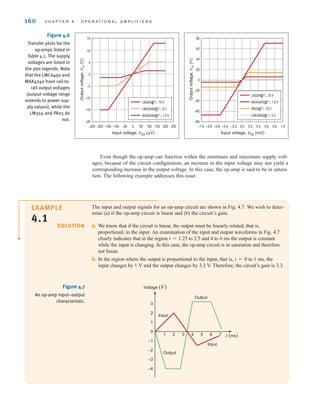
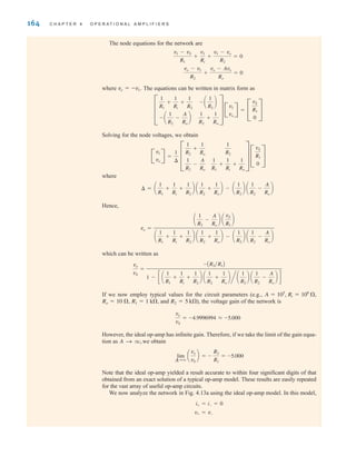
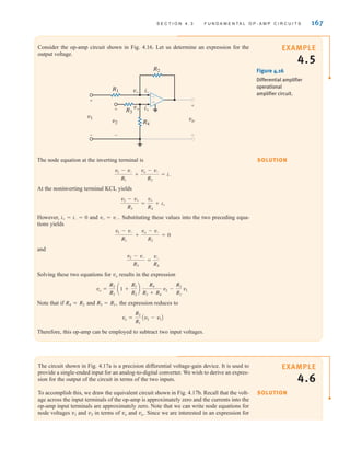
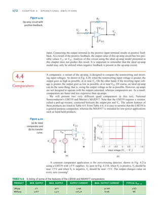
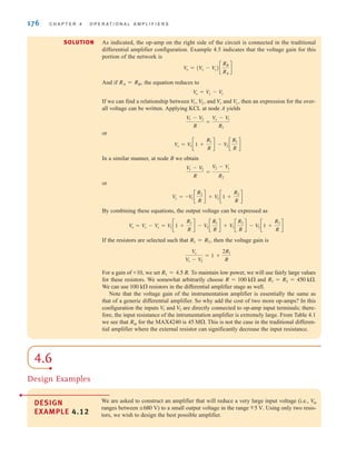
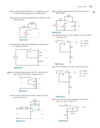
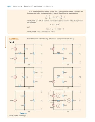
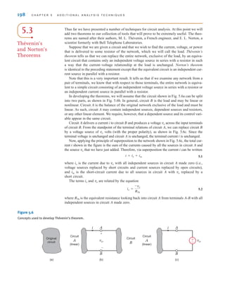
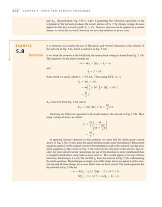
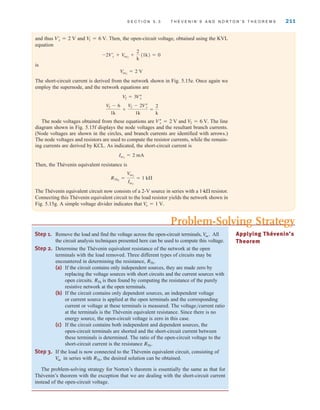
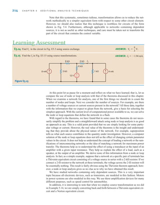
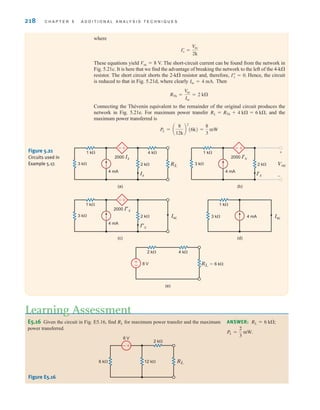
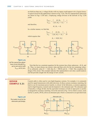
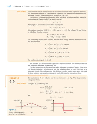
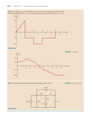
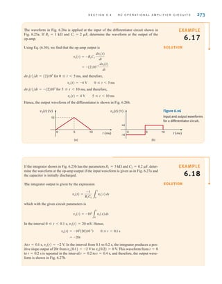
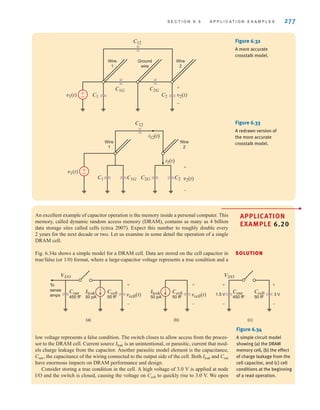
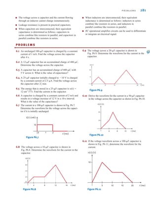
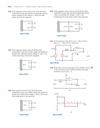
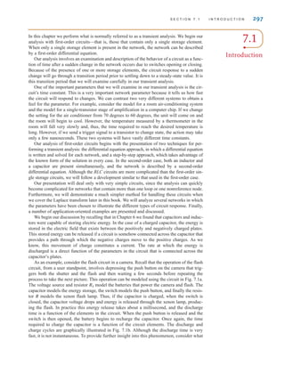
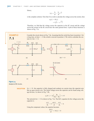
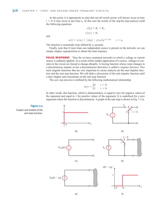
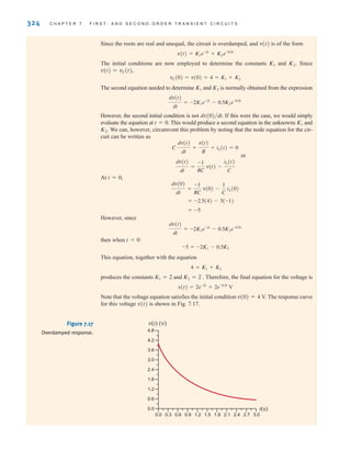
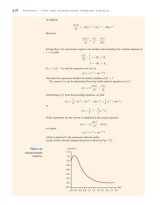
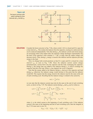
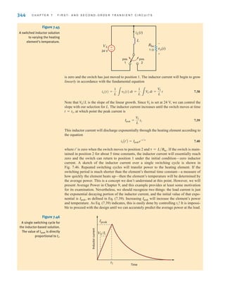
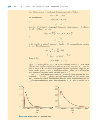
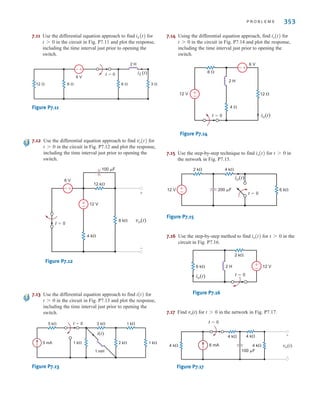
![6 C H A P T E R 1 B A S I C C O N C E P T S
Suppose that your car will not start. To determine whether the battery is faulty, you turn on
the light switch and find that the lights are very dim, indicating a weak battery. You borrow
a friend’s car and a set of jumper cables. However, how do you connect his car’s battery to
yours? What do you want his battery to do?
Essentially, his car’s battery must supply energy to yours, and therefore it should be
connected in the manner shown in Fig. 1.10. Note that the positive current leaves the posi-
tive terminal of the good battery (supplying energy) and enters the positive terminal of the
weak battery (absorbing energy). Note that the same connections are used when charging a
battery.
EXAMPLE
1.1
SOLUTION
I
I
Good
battery
Weak
battery
+ – + –
Figure 1.10
Diagram for Example 1.1.
In practical applications there are often considerations other than simply the electrical
relations (e.g., safety). Such is the case with jump-starting an automobile. Automobile
batteries produce explosive gases that can be ignited accidentally, causing severe physical
injury. Be safe—follow the procedure described in your auto owner’s manual.
We have defined voltage in joules per coulomb as the energy required to move a positive
charge of 1 C through an element. If we assume that we are dealing with a differential amount
of charge and energy, then
1.2
Multiplying this quantity by the current in the element yields
1.3
which is the time rate of change of energy or power measured in joules per second, or watts
(W). Since, in general, both v and i are functions of time, p is also a time-varying quantity.
Therefore, the change in energy from time to time can be found by integrating Eq. (1.3);
that is,
1.4
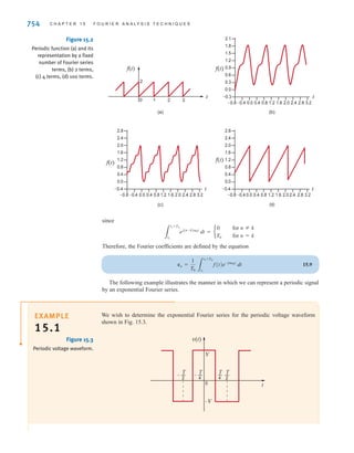
At this point, let us summarize our sign convention for power. To determine the sign of
any of the quantities involved, the variables for the current and voltage should be arranged as
shown in Fig. 1.11. The variable for the voltage v(t) is defined as the voltage across the ele-
ment with the positive reference at the same terminal that the current variable i(t) is entering.
This convention is called the passive sign convention and will be so noted in the remainder
of this book. The product of v and i, with their attendant signs, will determine the magnitude
and sign of the power. If the sign of the power is positive, power is being absorbed by the ele-
ment; if the sign is negative, power is being supplied by the element.
¢w =
3
t2
t1
p dt =
3
t2
t1
vi dt
t2
t1
vi =
dw
dq
a
dq
dt
b =
dw
dt
= p
v =
dw
dq
i(t)
v(t)
+
–
The passive sign convention
is used to determine whether
power is being absorbed or
supplied.
[ h i n t ]
Figure 1.11
Sign convention for power.
irwin01_001-024hr.qxd 30-06-2010 13:16 Page 6](https://image.slidesharecdn.com/basic-engineering-circuit-analysis-10th-irwin-220801002926-2b111212/85/basic-engineering-circuit-analysis-10th-Irwin-pdf-30-320.jpg)
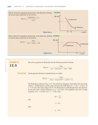
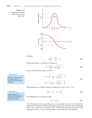
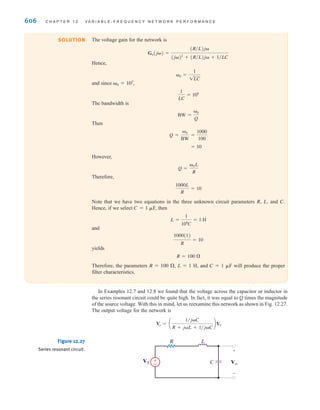
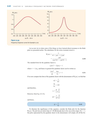
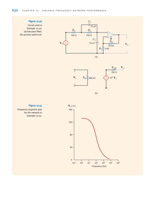
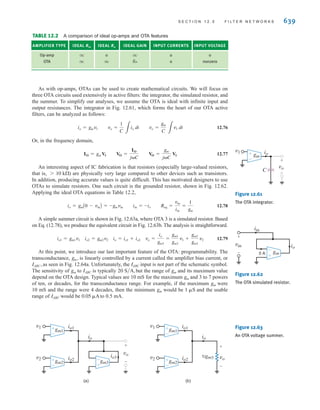
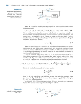
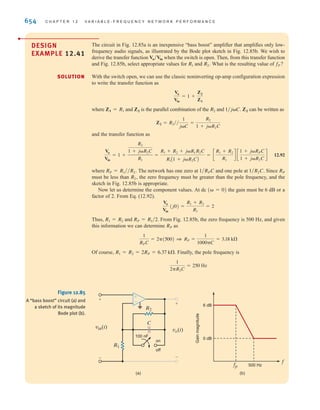
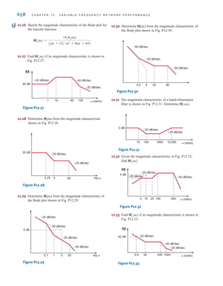
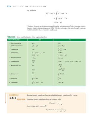
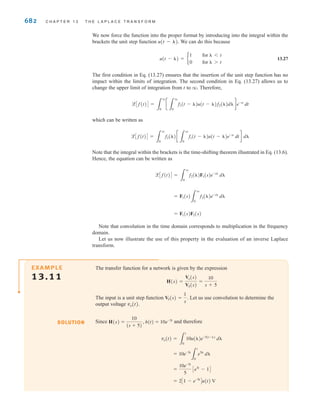
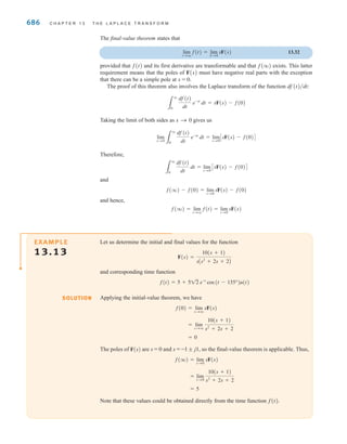
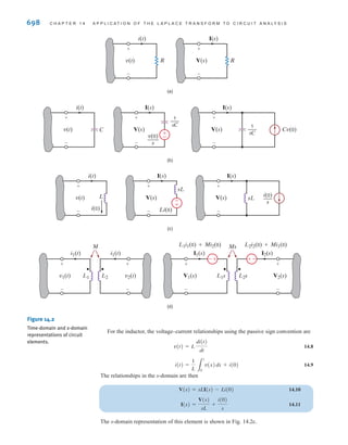
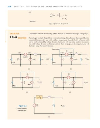
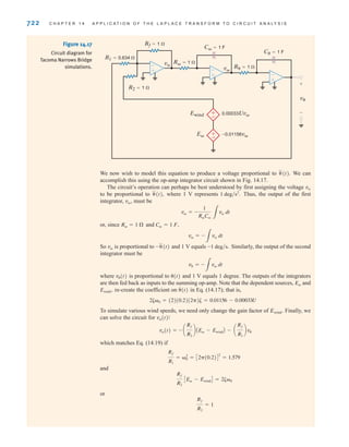
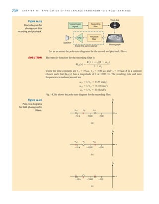
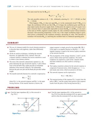
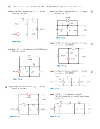
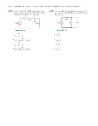
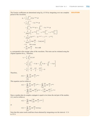
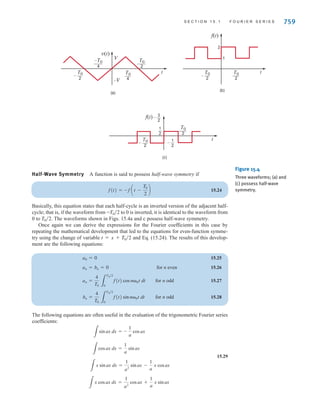
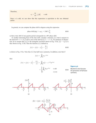
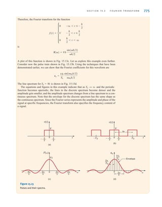
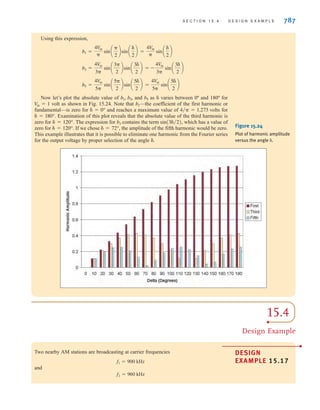
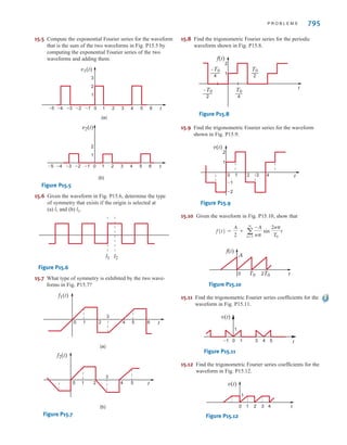
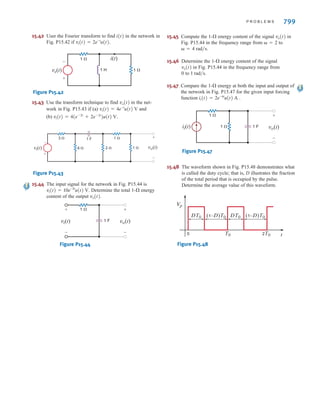
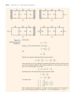
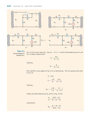
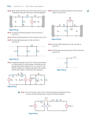
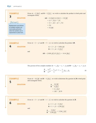
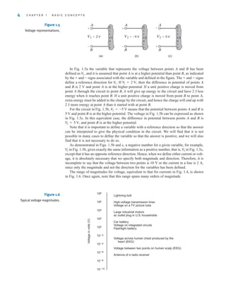
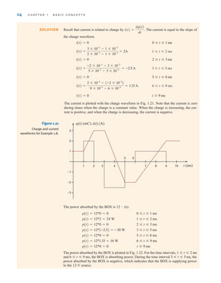
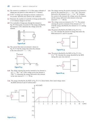
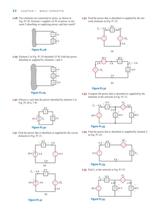
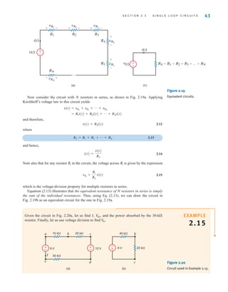
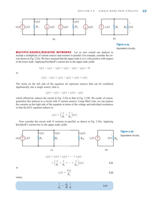
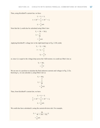
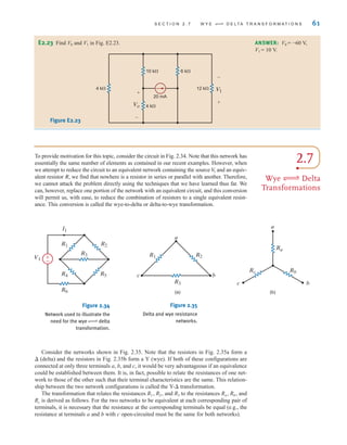
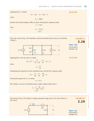
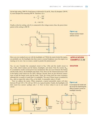
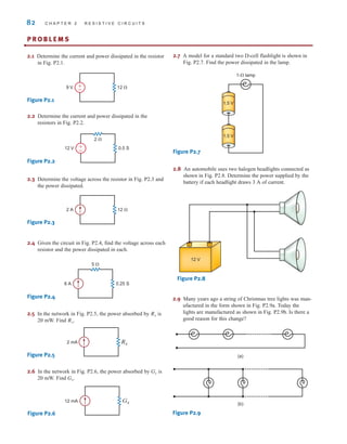
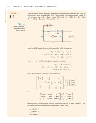
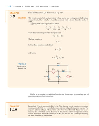
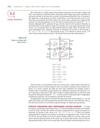
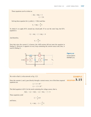
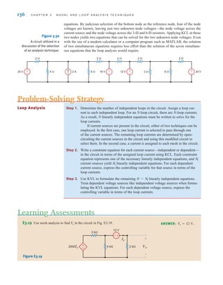
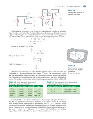
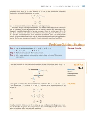
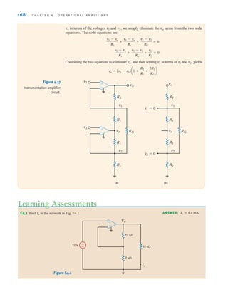
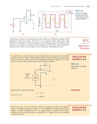
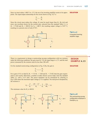
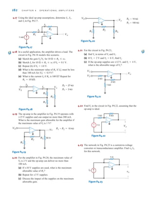
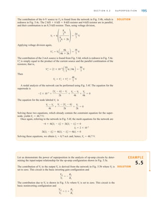
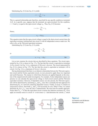
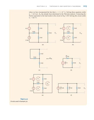
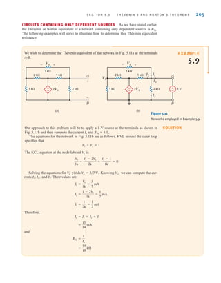
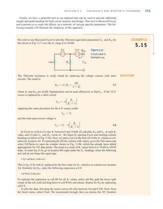
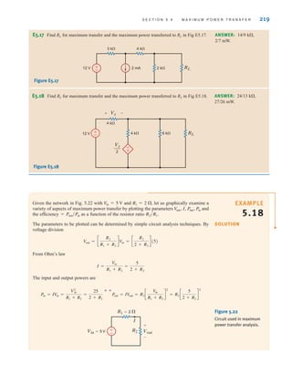
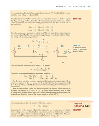
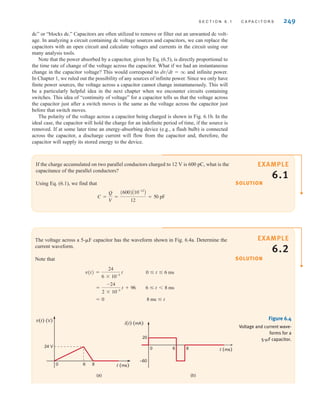
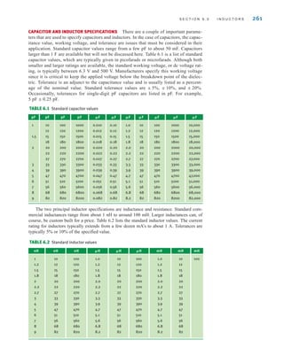
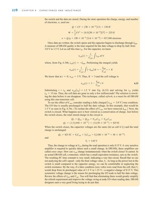
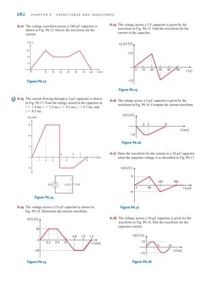
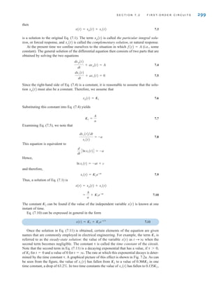
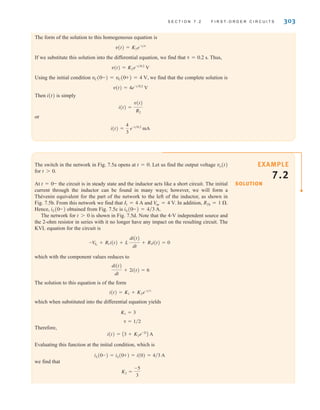
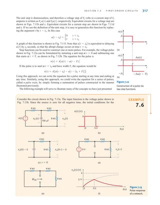
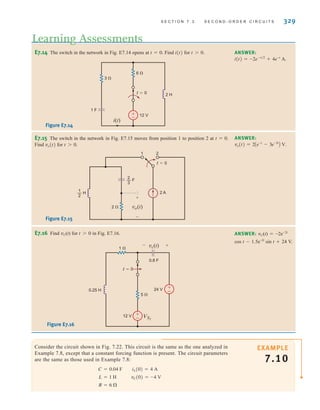
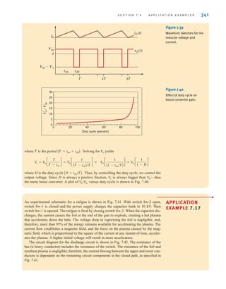
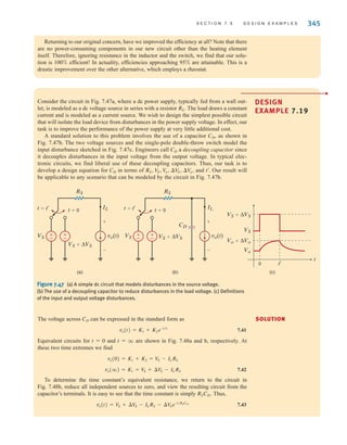
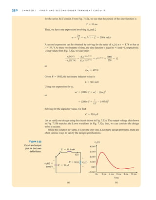
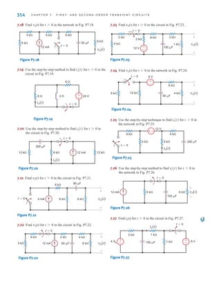
![DEPENDENT SOURCES In contrast to the independent sources, which produce a
particular voltage or current completely unaffected by what is happening in the remainder of
the circuit, dependent sources generate a voltage or current that is determined by a voltage or
current at a specified location in the circuit. These sources are very important because they
are an integral part of the mathematical models used to describe the behavior of many elec-
tronic circuit elements.
For example, metal-oxide-semiconductor field-effect transistors (MOSFETs) and bipolar
transistors, both of which are commonly found in a host of electronic equipment, are mod-
eled with dependent sources, and therefore the analysis of electronic circuits involves the use
of these controlled elements.
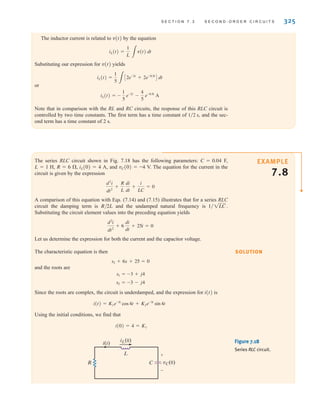
In contrast to the circle used to represent independent sources, a diamond is used to
represent a dependent or controlled source. Fig. 1.16 illustrates the four types of dependent
sources. The input terminals on the left represent the voltage or current that controls the
dependent source, and the output terminals on the right represent the output current or volt-
age of the controlled source. Note that in Figs. 1.16a and d, the quantities and  are dimen-
sionless constants because we are transforming voltage to voltage and current to current. This
is not the case in Figs. 1.16b and c; hence, when we employ these elements a short time later,
we must describe the units of the factors r and g.
10 C H A P T E R 1 B A S I C C O N C E P T S
The current flow is out of the positive terminal of the 24-V source, and therefore this
element is supplying (2)(24)=48 W of power. The current is into the positive terminals
of elements 1 and 2, and therefore elements 1 and 2 are absorbing (2)(6)=12 W and
(2)(18)=36 W, respectively. Note that the power supplied is equal to the power
absorbed.
SOLUTION
+
–
+
–
v=vS
+
–
+
–
(a) (b)
vS
vS i=gvS
v=riS
i=iS
iS
(c) (d)
iS
Figure 1.16
Four different types of
dependent sources.
Elements that are
connected in series have
the same current.
[ h i n t ]
E1.3 Find the power that is absorbed or supplied by the elements in Fig. E1.3.
Learning Assessment
ANSWER: Current source
supplies 36 W, element
1 absorbs 54 W, and
element 2 supplies 18 W.
Figure E1.3
12 V 6 V
I=3 A
3 A
I=3 A
+
+
–
–
+
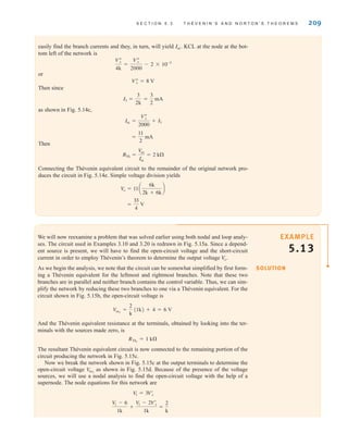
–
18 V
2
1
irwin01_001-024hr.qxd 30-06-2010 13:16 Page 10](https://image.slidesharecdn.com/basic-engineering-circuit-analysis-10th-irwin-220801002926-2b111212/85/basic-engineering-circuit-analysis-10th-Irwin-pdf-34-320.jpg)
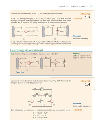
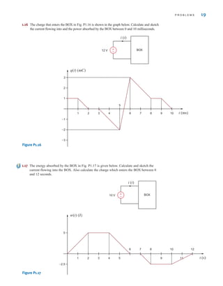
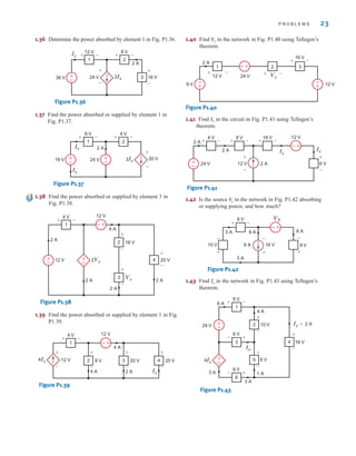
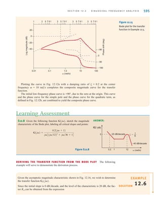
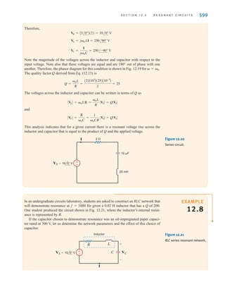
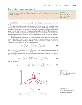
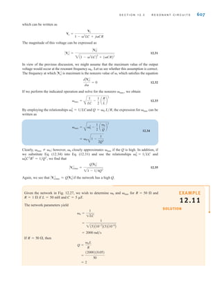
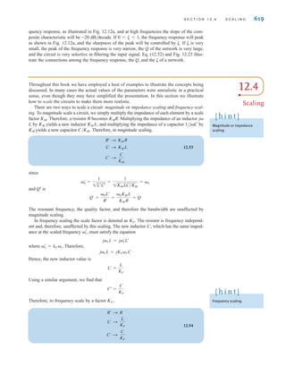
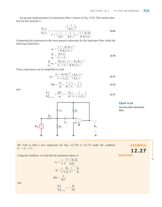
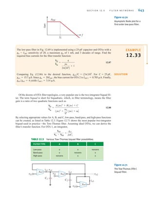
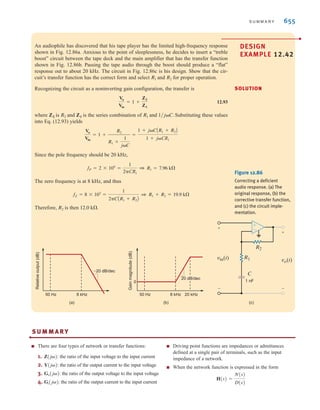
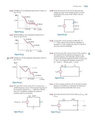
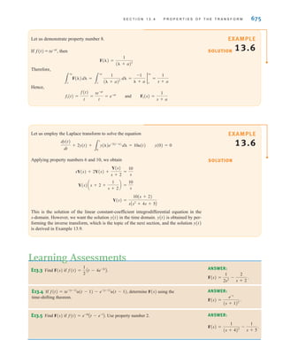
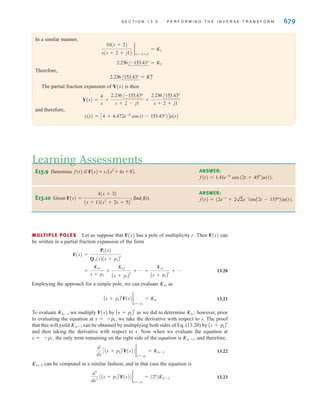
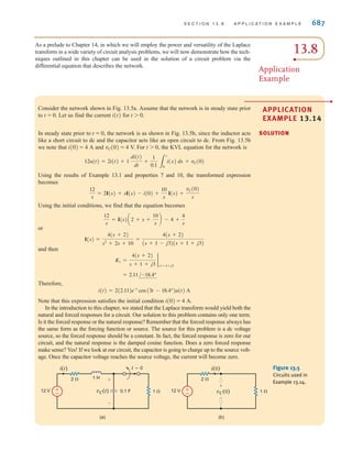
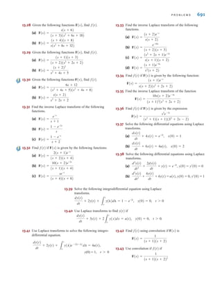
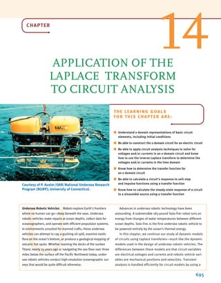
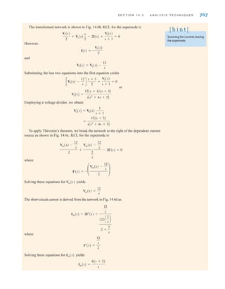
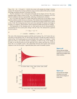
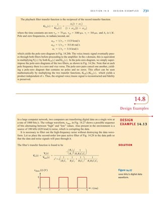
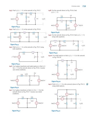
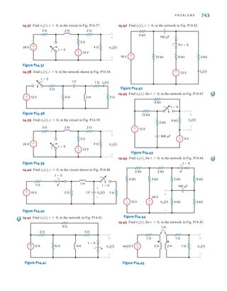
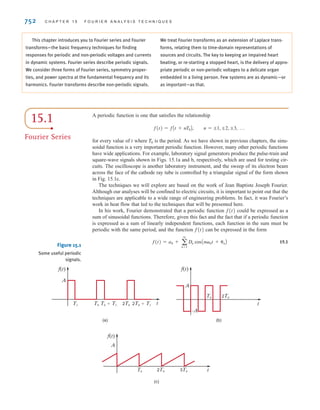
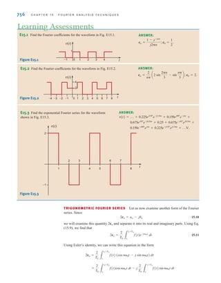
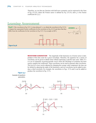
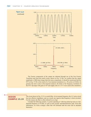
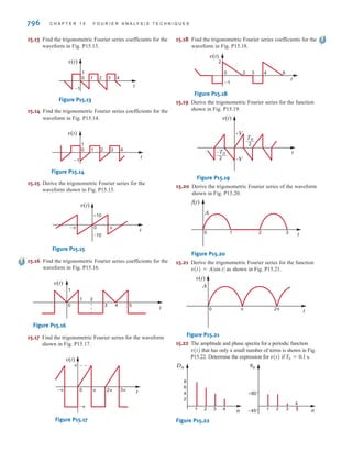
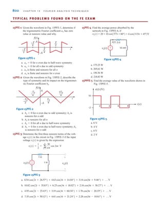
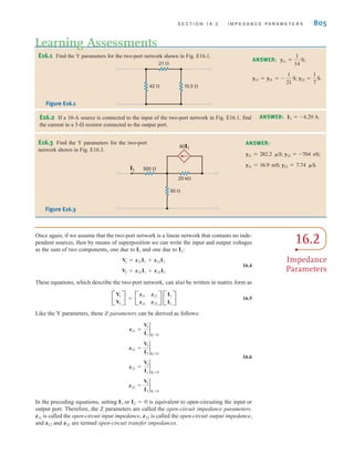
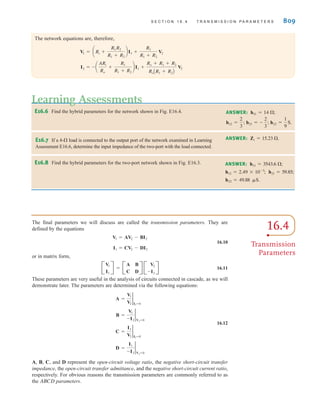
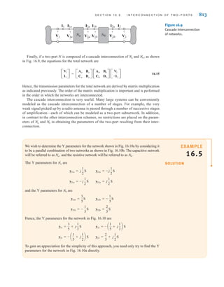
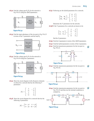
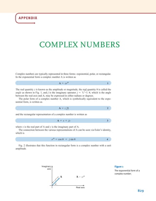
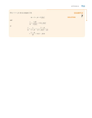
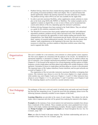
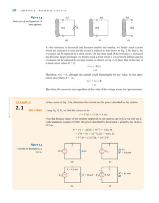
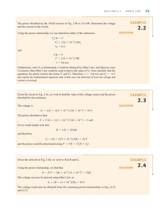
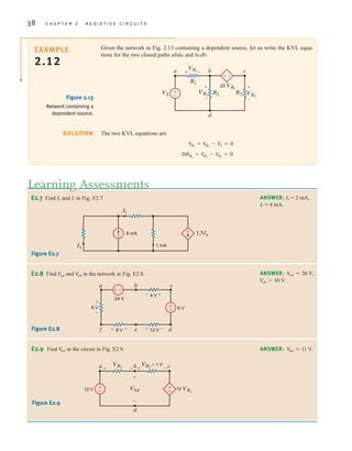
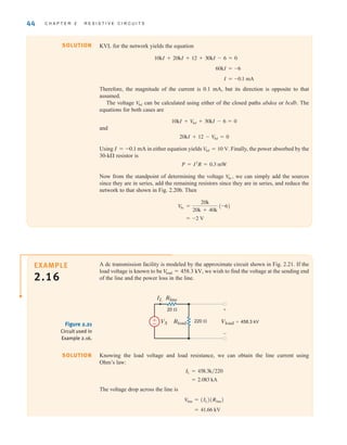
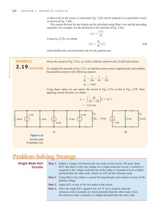
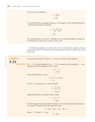
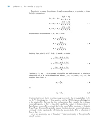
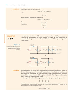
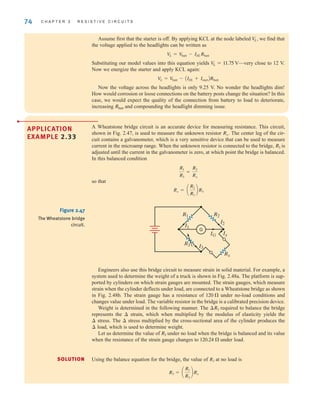
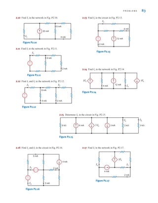
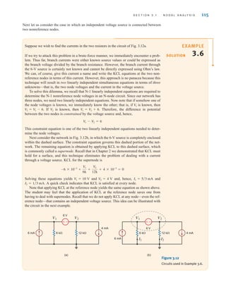
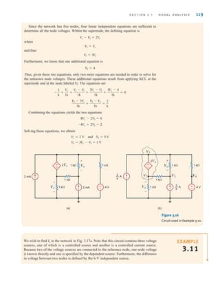
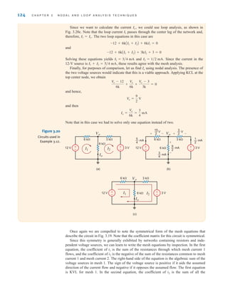
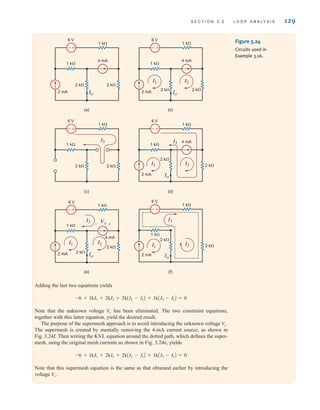
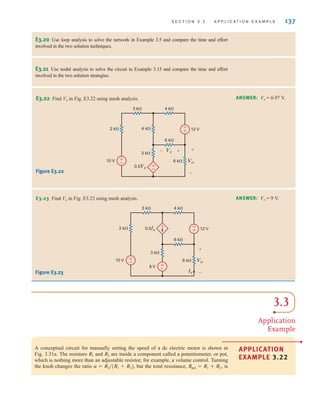
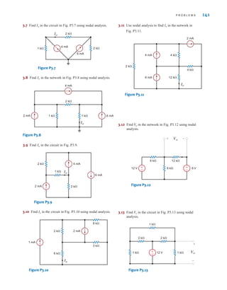
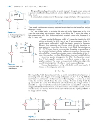
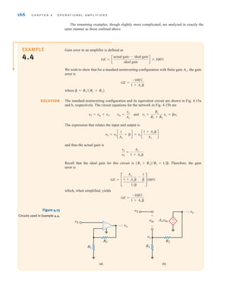
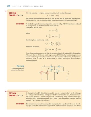
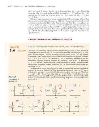
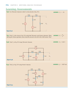
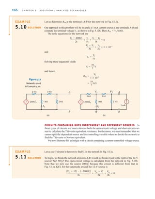
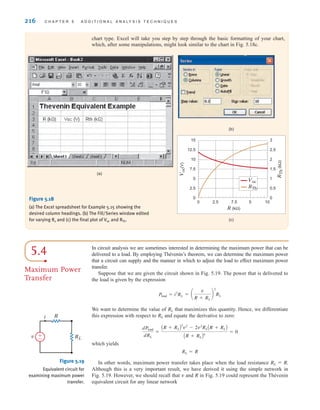
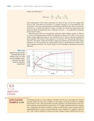
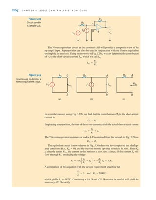
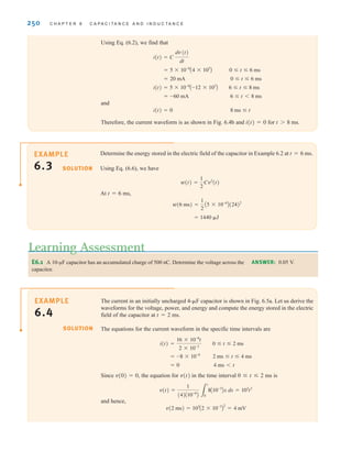
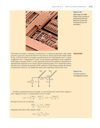
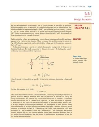
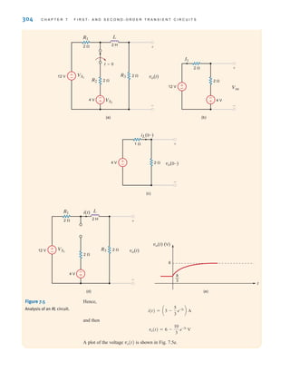
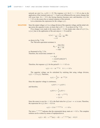
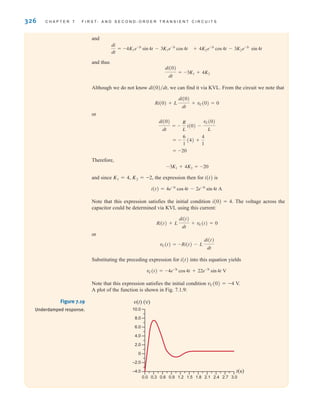
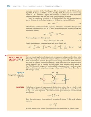
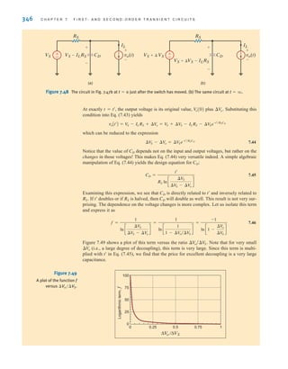
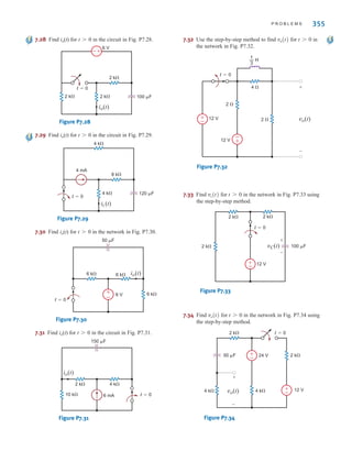
![26 C H A P T E R 2 R E S I S T I V E C I R C U I T S
2.1
Ohm’s Law
Ohm’s law is named for the German physicist Georg Simon Ohm, who is credited with
establishing the voltage–current relationship for resistance. As a result of his pioneering
work, the unit of resistance bears his name.
Ohm’s law states that the voltage across a resistance is directly proportional to the current
flowing through it. The resistance, measured in ohms, is the constant of proportionality
between the voltage and current.
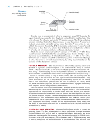
A circuit element whose electrical characteristic is primarily resistive is called a resistor
and is represented by the symbol shown in Fig. 2.1a. A resistor is a physical device that can
be purchased in certain standard values in an electronic parts store. These resistors, which
find use in a variety of electrical applications, are normally carbon composition or wire-
wound. In addition, resistors can be fabricated using thick oxide or thin metal films for use
in hybrid circuits, or they can be diffused in semiconductor integrated circuits. Some typical
discrete resistors are shown in Fig. 2.1b.
The mathematical relationship of Ohm’s law is illustrated by the equation
v(t)=R i(t), where R ⭌ 0 2.1
or equivalently, by the voltage–current characteristic shown in Fig. 2.2a. Note carefully the
relationship between the polarity of the voltage and the direction of the current. In addition,
note that we have tacitly assumed that the resistor has a constant value and therefore that the
voltage–current characteristic is linear.
The symbol ⍀ is used to represent ohms, and therefore,
1 ⍀=1 V/A
Although in our analysis we will always assume that the resistors are linear and are thus
described by a straight-line characteristic that passes through the origin, it is important that
readers realize that some very useful and practical elements do exist that exhibit a nonlinear
resistance characteristic; that is, the voltage–current relationship is not a straight line.
R
i(t)
v(t)
+
–
(a) (b)
Figure 2.1
(a) Symbol for a resistor;
(b) some practical devices.
(1), (2), and (3) are high-
power resistors. (4) and (5)
are high-wattage fixed
resistors. (6) is a high-
precision resistor. (7)–(12)
are fixed resistors with
different power ratings.
(Photo courtesy of Mark
Nelms and Jo Ann Loden)
The passive sign convention
will be employed in
conjunction with Ohm’s law.
[ h i n t ]
irwin02_025-100hr.qxd 22-07-2010 15:03 Page 26](https://image.slidesharecdn.com/basic-engineering-circuit-analysis-10th-irwin-220801002926-2b111212/85/basic-engineering-circuit-analysis-10th-Irwin-pdf-50-320.jpg)
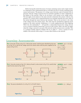
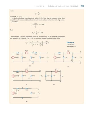
![in Fig. 2.5a will be used to describe the terms node, loop, and branch. A node is simply a
point of connection of two or more circuit elements. The reader is cautioned to note that,
although one node can be spread out with perfect conductors, it is still only one node. This
is illustrated in Fig. 2.5b, where the circuit has been redrawn. Node 5 consists of the entire
bottom connector of the circuit.
If we start at some point in the circuit and move along perfect conductors in any direction
until we encounter a circuit element, the total path we cover represents a single node.
Therefore, we can assume that a node is one end of a circuit element together with all the per-
fect conductors that are attached to it. Examining the circuit, we note that there are numerous
paths through it. A loop is simply any closed path through the circuit in which no node
is encountered more than once. For example, starting from node 1, one loop would contain the
elements and i1; another loop would contain and i1; and so on.
However, the path and i1 is not a loop because we have encountered node 3
twice. Finally, a branch is a portion of a circuit containing only a single element and the nodes
at each end of the element. The circuit in Fig. 2.5 contains eight branches.
Given the previous definitions, we are now in a position to consider Kirchhoff’s laws,
named after German scientist Gustav Robert Kirchhoff. These two laws are quite simple but
extremely important. We will not attempt to prove them because the proofs are beyond our
current level of understanding. However, we will demonstrate their usefulness and attempt to
make the reader proficient in their use. The first law is Kirchhoff’s current law (KCL), which
states that the algebraic sum of the currents entering any node is zero. In mathematical form
the law appears as
2.7
a
N
j=1
ij(t) = 0
R1, v1, R5, v2, R3,
R2, v1, v2, R4,
R1, v2, R4,
S E C T I O N 2 . 2 K I R C H H O F F ’ S L A W S 31
i1(t)
v2(t)
v1(t)
R1
R2
R5
R4
R3
(a)
R2
i1(t)
i2(t) i3(t)
i5(t)
v1(t)
v2(t)
i7(t)
i4(t)
i6(t)
i8(t)
R1
R4 R5
(b)
1
4
5
2
3
R3
–
±
±
–
±
–
–
±
Figure 2.5
Circuit used to illustrate KCL.
KCL is an extremely important
and useful law.
[ h i n t ]
2.2
Kirchhoff’s Laws
The circuits we have considered previously have all contained a single resistor, and we have
analyzed them using Ohm’s law. At this point we begin to expand our capabilities to handle
more complicated networks that result from an interconnection of two or more of these sim-
ple elements. We will assume that the interconnection is performed by electrical conductors
(wires) that have zero resistance—that is, perfect conductors. Because the wires have zero
resistance, the energy in the circuit is in essence lumped in each element, and we employ the
term lumped-parameter circuit to describe the network.
To aid us in our discussion, we will define a number of terms that will be employed
throughout our analysis. As will be our approach throughout this text, we will use examples
to illustrate the concepts and define the appropriate terms. For example, the circuit shown
irwin02_025-100hr.qxd 30-06-2010 13:14 Page 31](https://image.slidesharecdn.com/basic-engineering-circuit-analysis-10th-irwin-220801002926-2b111212/85/basic-engineering-circuit-analysis-10th-Irwin-pdf-55-320.jpg)
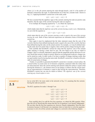
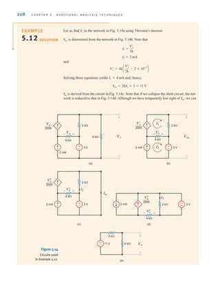
![for labeling voltages are shown in Fig. 2.11. The usefulness of the arrow notation stems from
the fact that we may want to label the voltage between two points that are far apart in a
network. In this case, the other notations are often confusing.
In general, the mathematical representation of Kirchhoff’s voltage law is
2.8
where vj(t) is the voltage across the jth branch (with the proper reference direction) in a loop
containing N voltages. This expression is analogous to Eq. (2.7) for Kirchhoff’s current law.
a
N
j=1
vj(t) = 0
S E C T I O N 2 . 2 K I R C H H O F F ’ S L A W S 37
1 1
(a)
Vx=Vab
a
b
+
–
1
a
b
+
–
1
Vx=Vo
+
–
Vx=Vo
+
–
Vo
(b)
Vx=Vab=Vo
(d)
Vo
+
–
Vo
+
–
(c)
Vo
Figure 2.11
Equivalent forms for labeling
voltage.
SOLUTION
EXAMPLE
2.11
Consider the network in Fig. 2.12a. Let us apply KVL to determine the voltage between two
points. Specifically, in terms of the double-subscript notation, let us find and V
ec.
V
ae
The circuit is redrawn in Fig. 2.12b. Since points a and e as well as e and c are not physi-
cally close, the arrow notation is very useful. Our approach to determining the unknown
voltage is to apply KVL with the unknown voltage in the closed path. Therefore, to deter-
mine we can use the path aefa or abcdea. The equations for the two paths in which
is the only unknown are
and
Note that both equations yield Even before calculating we could calculate
using the path cdec or cefabc. However, since is now known, we can also use the path
ceabc. KVL for each of these paths is
and
Each of these equations yields V
ec = -10 V.
-V
ec - V
ae + 16 - 12 = 0
-V
ec + 10 - 24 + 16 - 12 = 0
4 + 6 + V
ec = 0
V
ae
V
ec
V
ae,
V
ae = 14 V.
16 - 12 + 4 + 6 - V
ae = 0
Vae + 10 - 24 = 0
V
ae
V
ae
Vae Vec
(a) (b)
R1
R4 R3
R2
24 V
16 V
6 V
10 V
+ +
–
–
–
+
+
–
12 V
4 V
f d
b
e
a c
24 V
16 V
6 V
10 V
+ +
–
–
–
+
+
–
12 V
4 V
f d
b
e
a c
±
–
+
-
±
–
+
-
Figure 2.12
Network used in
Example 2.11.
KVL is an extremely important
and useful law.
[ h i n t ]
irwin02_025-100hr.qxd 30-06-2010 13:14 Page 37](https://image.slidesharecdn.com/basic-engineering-circuit-analysis-10th-irwin-220801002926-2b111212/85/basic-engineering-circuit-analysis-10th-Irwin-pdf-61-320.jpg)
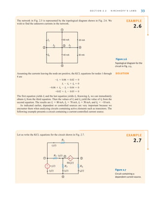
![S E C T I O N 2 . 3 S I N G L E - L O O P C I R C U I T S 39
Before proceeding with the analysis of simple circuits, it is extremely important that we
emphasize a subtle but very critical point. Ohm’s law as defined by the equation V=IR
refers to the relationship between the voltage and current as defined in Fig. 2.14a. If the direc-
tion of either the current or the voltage, but not both, is reversed, the relationship between the
current and the voltage would be V=–IR. In a similar manner, given the circuit in
Fig. 2.14b, if the polarity of the voltage between the terminals A and B is specified as shown,
then the direction of the current I is from point B through R to point A. Likewise, in
Fig. 2.14c, if the direction of the current is specified as shown, then the polarity of the voltage
must be such that point D is at a higher potential than point C and, therefore, the arrow rep-
resenting the voltage V is from point C to point D.
The subtleties associated
with Ohm’s law, as described
here, are important and must
be adhered to in order to
ensure that the variables
have the proper sign.
[ h i n t ]
(a) (b) (c)
V
I
R
A
B
+
–
V
I
R
A
B
-
+
V
I
R
C D
Figure 2.14
Circuits used to explain
Ohm’s law.
2.3
Single-Loop
Circuits
VOLTAGE DIVISION At this point we can begin to apply the laws presented earlier to the
analysis of simple circuits. To begin, we examine what is perhaps the simplest circuit—a
single closed path, or loop, of elements.
Applying KCL to every node in a single-loop circuit reveals that the same current flows
through all elements. We say that these elements are connected in series because they carry
the same current. We will apply Kirchhoff’s voltage law and Ohm’s law to the circuit to
determine various quantities in the circuit.
Our approach will be to begin with a simple circuit and then generalize the analysis to more
complicated ones. The circuit shown in Fig. 2.15 will serve as a basis for discussion. This cir-
cuit consists of an independent voltage source that is in series with two resistors. We have
assumed that the current flows in a clockwise direction. If this assumption is correct, the
solution of the equations that yields the current will produce a positive value. If the current is
actually flowing in the opposite direction, the value of the current variable will simply be
negative, indicating that the current is flowing in a direction opposite to that assumed. We have
also made voltage polarity assignments for and These assignments have been made
using the convention employed in our discussion of Ohm’s law and our choice for the direc-
tion of i(t)—that is, the convention shown in Fig. 2.14a.
Applying Kirchhoff’s voltage law to this circuit yields
or
However, from Ohm’s law we know that
Therefore,
v(t)=R1i(t)+R2i(t)
Solving the equation for i(t) yields
2.9
i(t) =
v(t)
R1 + R2
vR2
= R2i(t)
vR1
= R1i(t)
v(t) = vR1
+ vR2
-v(t) + vR1
+ vR2
= 0
vR2
.
vR1
±
–
vR1
vR2
R1
R2
v(t)
i(t)
+
–
+
–
Figure 2.15
Single-loop circuit.
irwin02_025-100hr.qxd 30-06-2010 13:14 Page 39](https://image.slidesharecdn.com/basic-engineering-circuit-analysis-10th-irwin-220801002926-2b111212/85/basic-engineering-circuit-analysis-10th-Irwin-pdf-63-320.jpg)
![Knowing the current, we can now apply Ohm’s law to determine the voltage across each
resistor:
2.10
Similarly,
2.11
Though simple, Eqs. (2.10) and (2.11) are very important because they describe the oper-
ation of what is called a voltage divider. In other words, the source voltage v(t) is divided
between the resistors and in direct proportion to their resistances.
In essence, if we are interested in the voltage across the resistor we bypass the calcu-
lation of the current i(t) and simply multiply the input voltage v(t) by the ratio
As illustrated in Eq. (2.10), we are using the current in the calculation, but not explicitly.
Note that the equations satisfy Kirchhoff’s voltage law, since
-v(t) +
R1
R1 + R2
v(t) +
R2
R1 + R2
v(t) = 0
R1
R1 + R2
R1,
R2
R1
vR2
=
R2
R1 + R2
v(t)
=
R1
R1 + R2
v(t)
= R1 c
v(t)
R1 + R2
d
vR1
= R1i(t)
40 C H A P T E R 2 R E S I S T I V E C I R C U I T S
Consider the circuit shown in Fig. 2.16. The circuit is identical to Fig. 2.15 except that
is a variable resistor such as the volume control for a radio or television set. Suppose that
and R2 = 30 k.
R1 = 90 k,
V
S = 9 V,
R1
EXAMPLE
2.13
SOLUTION
VS
V2
R1
I
R2
+
–
±
–
Figure 2.16
Voltage-divider circuit.
Let us examine the change in both the voltage across and the power absorbed in this
resistor as is changed from 90 k to 15 k.
Since this is a voltage-divider circuit, the voltage can be obtained directly as
= 2.25 V
= c
30k
90k + 30k
d (9)
V2 = c
R2
R1 + R2
d V
S
V
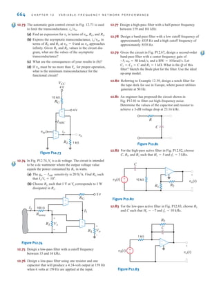
2
R1
R2
The manner in which voltage
divides between two
series resistors.
[ h i n t ]
irwin02_025-100hr.qxd 30-06-2010 13:14 Page 40](https://image.slidesharecdn.com/basic-engineering-circuit-analysis-10th-irwin-220801002926-2b111212/85/basic-engineering-circuit-analysis-10th-Irwin-pdf-64-320.jpg)
![where
2.16
2.17
Therefore, the equivalent resistance of two resistors connected in parallel is equal to the
product of their resistances divided by their sum. Note also that this equivalent resistance
is always less than either or Hence, by connecting resistors in parallel we reduce the
overall resistance. In the special case when the equivalent resistance is equal to half
of the value of the individual resistors.
The manner in which the current i(t) from the source divides between the two branches
is called current division and can be found from the preceding expressions. For example,
2.18
=
R1R2
R1 + R2
i(t)
v(t) = Rpi(t)
R1 = R2,
R2.
R1
Rp
Rp =
R1R2
R1 + R2
1
Rp
=
1
R1
+
1
R2
46 C H A P T E R 2 R E S I S T I V E C I R C U I T S
The parallel resistance
equation.
[ h i n t ]
CURRENT DIVISION An important circuit is the single-node-pair circuit. If we apply KVL to
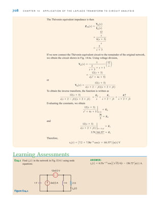
every loop in a single-node-pair circuit, we discover that all of the elements have the same volt-
age across them and, therefore, are said to be connected in parallel. We will, however, apply
Kirchhoff’s current law and Ohm’s law to determine various unknown quantities in the circuit.
Following our approach with the single-loop circuit, we will begin with the simplest case
and then generalize our analysis. Consider the circuit shown in Fig. 2.22. Here we have an
independent current source in parallel with two resistors.
R2
R1 v(t)
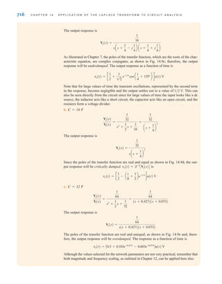
i(t)
i1(t) i2(t)
+
–
Figure 2.22
Simple parallel circuit.
Since all of the circuit elements are in parallel, the voltage v(t) appears across each of
them. Furthermore, an examination of the circuit indicates that the current i(t) is into the
upper node of the circuit and the currents i1(t) and i2(t) are out of the node. Since KCL
essentially states that what goes in must come out, the question we must answer is how i1(t)
and i2(t) divide the input current i(t).
Applying Kirchhoff’s current law to the upper node, we obtain
i(t)=i1(t)+i2(t)
and, employing Ohm’s law, we have
=
v(t)
Rp
= a
1
R1
+
1
R2
bv(t)
i(t) =
v(t)
R1
+
v(t)
R2
2.4
Single-Node-Pair
Circuits
irwin02_025-100hr.qxd 30-06-2010 13:14 Page 46](https://image.slidesharecdn.com/basic-engineering-circuit-analysis-10th-irwin-220801002926-2b111212/85/basic-engineering-circuit-analysis-10th-Irwin-pdf-70-320.jpg)
![S E C T I O N 2 . 4 S I N G L E - N O D E - P A I R C I R C U I T S 47
The manner in which
current divides between
two parallel resistors.
[ h i n t ]
Given the network in Fig. 2.23a, let us find and
First, it is important to recognize that the current source feeds two parallel paths. To empha-
size this point, the circuit is redrawn as shown in Fig. 2.23b. Applying current division,
we obtain
and
Note that the larger current flows through the smaller resistor, and vice versa. In addition,
note that if the resistances of the two paths are equal, the current will divide equally between
them. KCL is satisfied since I1+I2=0.9 mA.
The voltage can be derived using Ohm’s law as
The problem can also be approached in the following manner. The total resistance seen by
the current source is 40 k, that is, 60 k in parallel with the series combination of 40 k
and 80 k, as shown in Fig. 2.23c. The voltage across the current source is then
Now that is known, we can apply voltage division to find Vo:
= 24 V
= a
80k
120k
b36
V
o = a
80k
80k + 40k
bV
1
V
1
= 36 V
V
1 = A0.9 * 10-3
B40k
= 24 V
V
o = 80kI2
V
o
= 0.3 mA
I2 = c
60k
60k + (40k + 80k)
d A0.9 * 10-3
B
= 0.6 mA
I1 = c
40k + 80k
60k + (40k + 80k)
d A0.9 * 10-3
B
Vo.
I1, I2,
and
2.19
and
2.20
Eqs. (2.19) and (2.20) are mathematical statements of the current-division rule.
=
R1
R1 + R2
i(t)
i2(t) =
v(t)
R2
i1(t) =
R2
R1 + R2
i(t)
i1(t) =
v(t)
R1
SOLUTION
EXAMPLE
2.17
irwin02_025-100hr.qxd 30-06-2010 13:14 Page 47](https://image.slidesharecdn.com/basic-engineering-circuit-analysis-10th-irwin-220801002926-2b111212/85/basic-engineering-circuit-analysis-10th-Irwin-pdf-71-320.jpg)
![S E C T I O N 2 . 1 1 D E S I G N E X A M P L E S 77
Rearranging the equation yields
A second expression involving and can be developed by considering the case when
are all on, which causes to reach its minimum value of 9–5%, or 8.55 V. Now, the
effective resistance of the lamps is five 1.8- resistors in parallel, or The corre-
sponding expression for is
which can be rewritten in the form
Substituting the value determined for into the preceding equation yields
or
and so for
R2 = 178.3
R2
R1 = 48.1
R1 = 360[1.4 - 1 - 0.27]
R1兾R2
360R1
R2
+ 360 + R1
360
=
12
8.55
= 1.4
V2 = 8.55 = 12c
R2兾兾360
R1 + AR2兾兾360B
d
V
2
360 .
k
V
2
L3–L7
R2
R1
R1
R2
= 0.27
•
DESIGN
EXAMPLE 2.35
•
DESIGN
EXAMPLE 2.35
SOLUTION
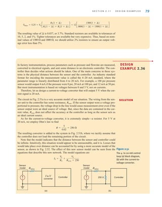
Let’s design a circuit that produces a 5-V output from a 12-V input. We will arbitrarily fix
the power consumed by the circuit at 240 mW. Finally, we will choose the best possible
standard resistor values from Table 2.1 and calculate the percent error in the output voltage
that results from that choice.
The simple voltage divider, shown in Fig. 2.50, is ideally suited for this application. We
know that is given by
which can be written as
Since all of the circuit’s power is supplied by the 12-V source, the total power is given by
Using the second equation to eliminate we find that has a lower limit of
Substituting these results into the second equation yields the lower limit of that is
Thus, we find that a significant portion of Table 2.1 is not applicable to this design.
However, determining the best pair of resistor values is primarily a trial-and-error operation
R1 = R2 c
V
in
V
o
- 1d 350
R1,
R2
V
oV
in
P
=
(5)(12)
0.24
= 250
R2
R1,
P =
V2
in
R1 + R2
0.24
R1 = R2 c
V
in
V
o
- 1d
V
o = V
in c
R2
R1 + R2
d
V
o
R1
12 V
R2 Vo=5 V
+
-
±
–
Figure 2.50
A simple voltage divider
irwin02_025-100hr.qxd 30-06-2010 13:14 Page 77](https://image.slidesharecdn.com/basic-engineering-circuit-analysis-10th-irwin-220801002926-2b111212/85/basic-engineering-circuit-analysis-10th-Irwin-pdf-101-320.jpg)

![The voltage is the voltage at node 1 with respect to the reference node 3.
Similarly, the voltage is the voltage at node 2 with respect to node 3. In addition,
however, the voltage at node 1 with respect to node 2 is ±6 V, and the voltage at node 2 with
respect to node 1 is -6 V. Furthermore, since the current will flow from the node of higher
potential to the node of lower potential, the current in is from top to bottom, the current
in is from left to right, and the current in is from bottom to top.
These concepts have important ramifications in our daily lives. If a man were hanging in
midair with one hand on one line and one hand on another and the dc line voltage of each
line was exactly the same, the voltage across his heart would be zero and he would be safe.
If, however, he let go of one line and let his feet touch the ground, the dc line voltage would
then exist from his hand to his foot with his heart in the middle. He would probably be dead
the instant his foot hit the ground.
In the town where we live, a young man tried to retrieve his parakeet that had escaped its
cage and was outside sitting on a power line. He stood on a metal ladder and with a metal
pole reached for the parakeet; when the metal pole touched the power line, the man was killed
instantly. Electric power is vital to our standard of living, but it is also very dangerous. The
material in this book does not qualify you to handle it safely. Therefore, always be extreme-
ly careful around electric circuits.
Now as we begin our discussion of nodal analysis, our approach will be to begin with sim-
ple cases and proceed in a systematic manner to those that are more challenging. Numerous
examples will be the vehicle used to demonstrate each facet of this approach. Finally, at the
end of this section, we will outline a strategy for attacking any circuit using nodal analysis.
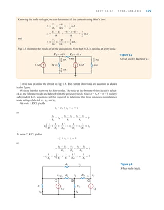
CIRCUITS CONTAINING ONLY INDEPENDENT CURRENT SOURCES Consider
the network shown in Fig. 3.4. Note that this network contains three nodes, and thus we know
that exactly linearly independent KCL equations will be required to
determine the unknown node voltages. First, we select the bottom node as the
reference node, and then the voltage at the two remaining nodes labeled and will be
measured with respect to this node.
The branch currents are assumed to flow in the directions indicated in the figures. If one
or more of the branch currents are actually flowing in a direction opposite to that assumed,
the analysis will simply produce a branch current that is negative.
Applying KCL at node 1 yields
Using Ohm’s law (i=Gv) and noting that the reference node is at zero potential, we obtain
or
KCL at node 2 yields
or
which can be expressed as
-G2v1 + AG2 + G3Bv2 = -iB
-G2Av1 - v2B + iB + G3Av2 - 0B = 0
-i2 + iB + i3 = 0
AG1 + G2Bv1 - G2v2 = iA
-iA + G1Av1 - 0B + G2Av1 - v2B = 0
-iA + i1 + i2 = 0
v2
v1
N - 1 = 2
N - 1 = 3 - 1 = 2
R3
R2
R1
V
2 = -2 V
V
1 = 4 V
104 C H A P T E R 3 N O D A L A N D L O O P A N A LY S I S T E C H N I Q U E S
Employing the passive sign
convention.
[ h i n t ]
1 2
3
R1 R3
R2
iB
i3
i1
i2
iA
v1 v2
Figure 3.4
A three-node circuit.
irwin03_101-155hr.qxd 30-06-2010 13:12 Page 104](https://image.slidesharecdn.com/basic-engineering-circuit-analysis-10th-irwin-220801002926-2b111212/85/basic-engineering-circuit-analysis-10th-Irwin-pdf-128-320.jpg)
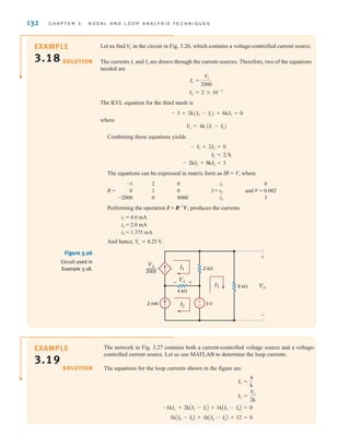
![S E C T I O N 3 . 1 N O D A L A N A LY S I S 113
E3.4 Find the node voltages in the circuit in Fig. E3.4.
Learning Assessments
ANSWER:
V2 = -8 V.
V
1 = 16 V,
E3.5 Find the voltage in the network in Fig. E3.5.
Vo ANSWER: Vo = 4 V.
4 mA
10 k⍀
10 k⍀
10 k⍀
Io
2Io
V1 V2
Figure E3.4
3 k⍀
2 mA 12 k⍀ 12 k⍀ Vo
+
-
Vx
6000
—
Vx
Figure E3.5
2 mA
6 k⍀
3 k⍀ 6 k⍀
2IA 1 k⍀
2 k⍀
Vo
+
–
IA
E3.6 Find in Fig. E3.6 using nodal analysis.
V
o ANSWER: = 0.952 V.
Vo
Figure E3.6
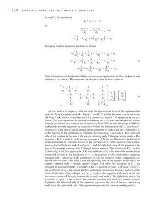
CIRCUITS CONTAINING INDEPENDENT VOLTAGE SOURCES As is our practice,
in our discussion of this topic we will proceed from the simplest case to more complicated
cases. The simplest case is that in which an independent voltage source is connected to the
reference node. The following example illustrates this case.
Consider the circuit shown in Fig. 3.11a. Let us determine all node voltages and branch currents.
This network has three nonreference nodes with labeled node voltages and Based
on our previous discussions, we would assume that in order to find all the node voltages we
would need to write a KCL equation at each of the nonreference nodes. The resulting three
linearly independent simultaneous equations would produce the unknown node voltages.
However, note that and are known quantities because an independent voltage source is
connected directly between the nonreference node and each of these nodes. Therefore,
and Furthermore, note that the current through the 9-kΩ resistor is
from left to right. We do not know or the current in the remain-
ing resistors. However, since only one node voltage is unknown, a single-node equation will
produce it. Applying KCL to this center node yields
V2
[12 - (-6)]兾9k = 2 mA
V3 = -6 V.
V1 = 12 V
V3
V1
V3.
V2,
V1, SOLUTION
EXAMPLE
3.5
irwin03_101-155hr.qxd 30-06-2010 13:12 Page 113](https://image.slidesharecdn.com/basic-engineering-circuit-analysis-10th-irwin-220801002926-2b111212/85/basic-engineering-circuit-analysis-10th-Irwin-pdf-137-320.jpg)
![114 C H A P T E R 3 N O D A L A N D L O O P A N A LY S I S T E C H N I Q U E S
or
from which we obtain
Once all the node voltages are known, Ohm’s law can be used to find the branch currents
shown in Fig. 3.11b. The diagram illustrates that KCL is satisfied at every node.
Note that the presence of the voltage sources in this example has simplified the analysis,
since two of the three linear independent equations are and We will
find that as a general rule, whenever voltage sources are present between nodes, the node
voltage equations that describe the network will be simpler.
V3 = -6 V.
V1 = 12 V
V2 =
3
2
V
V2 - 12
12k
+
V2
6k
+
V2 - (-6)
12k
= 0
V2 - V1
12k
+
V2 - 0
6k
+
V2 - V3
12k
= 0
-
+
±
–
±
–
V3
V1
V2
12 k⍀ 12 k⍀
9 k⍀
6 k⍀ 6 V
12 V
(a)
-
+
12 k⍀ 12 k⍀
9 k⍀
6 k⍀ 6 V
12 V
(b)
3
2
— V
2
k
— A
7
8k
— A
23
8k
— A
1
4k
— A
21
8k
— A
5
8k
— A
+12 V –6 V
Figure 3.11
Circuit used in
Example 3.5.
E3.7 Use nodal analysis to find the current in the network in Fig. E3.7.
Io
Learning Assessment
ANSWER: Io =
3
4
mA.
±
–
±
–
Vo
Io
6 k⍀ 6 k⍀
6 V 3 k⍀ 3 V
2 mA
6 k⍀
3 k⍀
6 k⍀
8 mA
12 V
1 k⍀
2 k⍀
Vo
+
–
±
–
Figure E3.7
Any time an independent
voltage source is connected
between the reference node
and a nonreference node,
the nonreference node volt-
age is known.
[ h i n t ]
E3.8 Find V0 in Fig. E3.8 using nodal analysis. ANSWER: V0 = 3.89 V.
Figure E3.8
irwin03_101-155hr.qxd 30-06-2010 13:12 Page 114](https://image.slidesharecdn.com/basic-engineering-circuit-analysis-10th-irwin-220801002926-2b111212/85/basic-engineering-circuit-analysis-10th-Irwin-pdf-138-320.jpg)
![through is The directions of the currents have been assumed. As was the case in the
nodal analysis, if the actual currents are not in the direction indicated, the values calculated will
be negative.
Applying KVL to the first loop yields
KVL applied to loop 2 yields
where
Substituting these values into the two KVL equations produces the two simultaneous
equations required to determine the two loop currents; that is,
or in matrix form
At this point, it is important to define what is called a mesh. A mesh is a special kind of loop
that does not contain any loops within it. Therefore, as we traverse the path of a mesh, we do not
encircle any circuit elements. For example, the network in Fig. 3.19 contains two meshes defined
by the paths A-B-E-F-A and B-C-D-E-B. The path A-B-C-D-E-F-A is a loop, but it is not a mesh.
Since the majority of our analysis in this section will involve writing KVL equations for meshes,
we will refer to the currents as mesh currents and the analysis as a mesh analysis.
B
R1 + R2 + R3
-R3
-R3
R3 + R4 + R5
R B
i1
i2
R = B
vS1
-vS2
R
-i1AR3B + i2AR3 + R4 + R5B = -vS2
i1AR1 + R2 + R3B - i2AR3B = vS1
v1 = i1R1, v2 = i1R2, v3 = Ai1 - i2BR3, v4 = i2R4, and v5 = i2R5.
+vS2 + v4 + v5 - v3 = 0
+v1 + v3 + v2 - vS1 = 0
i1 - i2.
R3
S E C T I O N 3 . 2 L O O P A N A LY S I S 123
The equations employ the
passive sign convention.
[ h i n t ]
±
–
–
±
A B C
F E D
vS1
v1
v2
vS2
v5
v4
R4
v3
R3
R1
R2 R5
i1 i2
+
-
+
+
-
-
- + - +
Figure 3.19
A two-loop circuit.
SOLUTION
EXAMPLE
3.12
Consider the network in Fig. 3.20a. We wish to find the current
We will begin the analysis by writing mesh equations. Note that there are no + and - signs
on the resistors. However, they are not needed, since we will apply Ohm’s law to each resis-
tive element as we write the KVL equations. The equation for the first mesh is
The KVL equation for the second mesh is
where
Solving the two simultaneous equations yields and Therefore,
All the voltages and currents in the network are shown in Fig. 3.20b. Recall
from nodal analysis that once the node voltages were determined, we could check our analy-
sis using KCL at the nodes. In this case, we know the branch currents and can use KVL around
any closed path to check our results. For example, applying KVL to the outer loop yields
0 = 0
-12 +
15
2
+
3
2
+ 3 = 0
Io = 3兾4 mA.
I2 = 1兾2 mA.
I1 = 5兾4 mA
Io = I1 - I2.
6kAI2 - I1B + 3kI2 + 3 = 0
-12 + 6kI1 + 6kAI1 - I2B = 0
Io.
irwin03_101-155hr.qxd 30-06-2010 13:12 Page 123](https://image.slidesharecdn.com/basic-engineering-circuit-analysis-10th-irwin-220801002926-2b111212/85/basic-engineering-circuit-analysis-10th-Irwin-pdf-147-320.jpg)
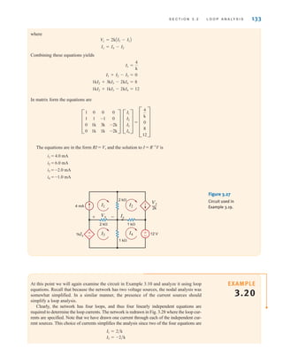
![128 C H A P T E R 3 N O D A L A N D L O O P A N A LY S I S T E C H N I Q U E S
-
+
4 mA
2 mA 3 V
2 k⍀
4 k⍀
6 k⍀
4 k⍀
Vo
+
-
I3
I1
I2
Figure 3.23
Circuit used in
Example 3.15.
What we have demonstrated in the previous example is the general approach for dealing
with independent current sources when writing KVL equations; that is, use one loop through
each current source. The number of “window panes” in the network tells us how many equa-
tions we need. Additional KVL equations are written to cover the remaining circuit elements
in the network. The following example illustrates this approach.
Let us find in the network in Fig. 3.24a.
First, we select two loop currents and such that passes directly through the 2-mA
source, and passes directly through the 4-mA source, as shown in Fig. 3.24b. Therefore,
two of our three linearly independent equations are
The remaining loop current must pass through the circuit elements not covered by the two
previous equations and cannot, of course, pass through the current sources. The path for this
remaining loop current can be obtained by open-circuiting the current sources, as shown in
Fig. 3.24c. When all currents are labeled on the original circuit, the KVL equation for this
last loop, as shown in Fig. 3.24d, is
Solving the equations yields
and therefore,
Next consider the supermesh technique. In this case the three mesh currents are specified
as shown in Fig. 3.24e, and since the voltage across the 4-mA current source is unknown,
it is assumed to be The mesh currents constrained by the current sources are
The KVL equations for meshes 2 and 3, respectively, are
-6 + 1kI3 + V
x + 1kAI3 - I1B = 0
2kI2 + 2kAI2 - I1B - V
x = 0
I2 - I3 = 4 * 10-3
I1 = 2 * 10-3
Vx.
Io = I1 - I2 - I3 =
-4
3
mA
I3 =
-2
3
mA
-6 + 1kI3 + 2kAI2 + I3B + 2kAI3 + I2 - I1B + 1kAI3 - I1B = 0
I3
I2 = 4 * 10-3
I1 = 2 * 10-3
I2
I1
I2
I1
Io
SOLUTION
In this case the 4-mA current
source is located on the
boundary between two mesh-
es. Thus, we will demonstrate
two techniques for dealing
with this type of situtation.
One is a special loop tech-
nique, and the other is known
as the supermesh approach.
[ h i n t ]
EXAMPLE
3.16
irwin03_101-155hr.qxd 30-06-2010 13:12 Page 128](https://image.slidesharecdn.com/basic-engineering-circuit-analysis-10th-irwin-220801002926-2b111212/85/basic-engineering-circuit-analysis-10th-Irwin-pdf-152-320.jpg)

![S U M M A R Y 179
facts imply that a new resistor value is needed and the output voltage should be shifted
down so that the minimum is zero. We begin by computing the necessary resistor value:
The resistor voltage will now range from to , or 1.25 to 6.25 V.
We must now design a circuit that shifts these voltage levels so that the range is 0 to 5 V.
One possible option for the level shifter circuit is the differential amplifier shown in
Fig. 4.30. Recall that the output voltage of this device is
Since we have already chosen R for a voltage span of 5 V, the gain of the amplifier should
be 1 (i.e., ). Clearly, the value of the required shift voltage is 1.25 V. However, we
can verify this value by inserting the minimum values into this last equation
and find
There is one caveat to this design. We don’t want the converter resistor, R, to affect
the differential amplifier, or vice versa. This means that the vast majority of the
4–20 mA current should flow entirely through R and not through the differential ampli-
fier resistors. If we choose and this requirement will be met. Therefore,
we might select so that their resistance values are more than 300
times that of R.
R1 = R2 = 100 k
R2 W R,
R1
V
shift = (312.5)(0.004) = 1.25 V
0 = [(312.5)(0.004) - V
shift]
R2
R1
R1 = R2
V
o = (V
I - V
shift)
R2
R1
(0.02)(312.5)
(0.004)(312.5)
R =
V
max - V
min
Imax - Imin
=
5 - 0
0.02 - 0.004
= 312.5
VI
Vshift
+
-
Vo
+
-
R2
R2
R1
R1
R
4–20 mA
Differential amplifier with shifter
±
–
–
±
Figure 4.30
A 4–20 mA to 0–5 V
converter circuit.
S U M M A R Y
■ Op-amps are characterized by
High-input resistance
Low-output resistance
Very high gain
■ The ideal op-amp is modeled using
■ Op-amp problems are typically analyzed by writing node
equations at the op-amp input terminals
■ The output of a comparator is dependent on the difference
in voltage at the input terminals
v+ = v-
i+ = i- = 0
•
irwin04-156-188hr.qxd 9-07-2010 14:17 Page 179](https://image.slidesharecdn.com/basic-engineering-circuit-analysis-10th-irwin-220801002926-2b111212/85/basic-engineering-circuit-analysis-10th-Irwin-pdf-203-320.jpg)

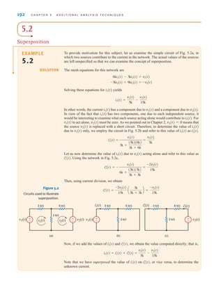

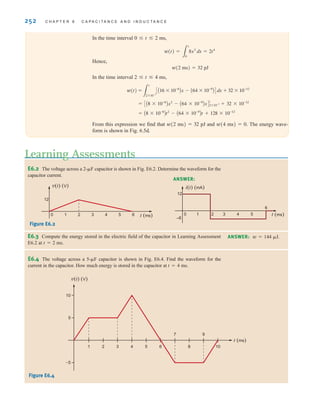
![6.1
Capacitors
A capacitor is a circuit element that consists of two conducting surfaces separated by a non-
conducting, or dielectric, material. A simplified capacitor and its electrical symbol are shown
in Fig. 6.1.
There are many different kinds of capacitors, and they are categorized by the type of
dielectric material used between the conducting plates. Although any good insulator can
serve as a dielectric, each type has characteristics that make it more suitable for particular
applications.
For general applications in electronic circuits (e.g., coupling between stages of amplifica-
tion), the dielectric material may be paper impregnated with oil or wax, mylar, polystyrene,
mica, glass, or ceramic.
Ceramic dielectric capacitors constructed of barium titanates have a large
capacitance-to-volume ratio because of their high dielectric constant. Mica, glass, and ceram-
ic dielectric capacitors will operate satisfactorily at high frequencies.
Aluminum electrolytic capacitors, which consist of a pair of aluminum plates separated
by a moistened borax paste electrolyte, can provide high values of capacitance in small vol-
umes. They are typically used for filtering, bypassing, and coupling, and in power supplies
and motor-starting applications. Tantalum electrolytic capacitors have lower losses and more
stable characteristics than those of aluminum electrolytic capacitors. Fig. 6.2 shows a variety
of typical discrete capacitors.
In addition to these capacitors, which we deliberately insert in a network for specific
applications, stray capacitance is present any time there is a difference in potential between
two conducting materials separated by a dielectric. Because this stray capacitance can cause
246 C H A P T E R 6 C A P A C I T A N C E A N D I N D U C T A N C E
Figure 6.2
Some typical capacitors.
(Courtesy of Mark Nelms and
Jo Ann Loden)
d
Dielectric
(a)
C
q(t)
v(t)
(b)
+
+
-
-
i=—
dq
dt
A
Figure 6.1
A capacitor and its
electrical symbol.
Note the use of the passive
sign convention.
[ h i n t ]
irwin06-245-295hr.qxd 9-07-2010 14:27 Page 246](https://image.slidesharecdn.com/basic-engineering-circuit-analysis-10th-irwin-220801002926-2b111212/85/basic-engineering-circuit-analysis-10th-Irwin-pdf-270-320.jpg)
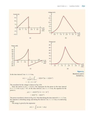
![S E C T I O N 6 . 3 C A P A C I T O R A N D I N D U C T O R C O M B I N A T I O N S 265
Determine the equivalent capacitance and the initial voltage for the circuit shown in Fig. 6.14.
Note that these capacitors must have been charged before they were connected in series or
else the charge of each would be equal and the voltages would be in the same direction.
The equivalent capacitance is
where all capacitance values are in microfarads.
Therefore, CS=1 F and, as seen from the figure, Note that the total
energy stored in the circuit is
However, the energy recoverable at the terminals is
= 4.5 J
=
1
2
C1 * 10-6
(-3)2
D
wCAt0B =
1
2
CSv2
(t)
= 31 J
wAt0B =
1
2
C2 * 10-6
(2)2
+ 3 * 10-6
(-4)2
+ 6 * 10-6
(-1)2
D
vAt0B = -3 V.
1
CS
=
1
2
+
1
3
+
1
6
SOLUTION
EXAMPLE
6.12
Therefore, Eq. (6.13) can be written as follows using Eq. (6.14):
6.15
6.16
where
and
6.17
Thus, the circuit in Fig. 6.13b is equivalent to that in Fig. 6.13a under the conditions stated
previously.
It is also important to note that since the same current flows in each of the series capaci-
tors, each capacitor gains the same charge in the same time period. The voltage across each
capacitor will depend on this charge and the capacitance of the element.
1
CS
= a
N
i=1
1
Ci
=
1
C1
+
1
C2
+ p +
1
CN
vAt0B = a
N
i=1
viAt0B
=
1
CS 3
t
t0
i(t)dt + vAt0B
v(t) = a a
N
i=1
1
Ci
b
3
t
t0
i(t)dt + a
N
i=1
viAt0B
4 V
3 F
2 F
6 F
v(t)
+
+
-
-
2 V
+ -
1 V
+ -
Figure 6.14
Circuit containing multiple
capacitors with initial
voltages.
Capacitors in series combine
like resistors in parallel.
[ h i n t ]
irwin06-245-295hr.qxd 9-07-2010 14:27 Page 265](https://image.slidesharecdn.com/basic-engineering-circuit-analysis-10th-irwin-220801002926-2b111212/85/basic-engineering-circuit-analysis-10th-Irwin-pdf-289-320.jpg)
![266 C H A P T E R 6 C A P A C I T A N C E A N D I N D U C T A N C E
Two previously uncharged capacitors are connected in series and then charged with a 12-V
source. One capacitor is 30 F and the other is unknown. If the voltage across the 30-F
capacitor is 8 V, find the capacitance of the unknown capacitor.
The charge on the 30-F capacitor is
Q=CV=(30 F)(8 V)=240 C
Since the same current flows in each of the series capacitors, each capacitor gains the same
charge in the same time period:
C =
Q
V
=
240 C
4V
= 60 F
SOLUTION
EXAMPLE
6.13
PARALLEL CAPACITORS To determine the equivalent capacitance of N capacitors
connected in parallel, we employ KCL. As can be seen from Fig. 6.15a,
6.18
6.19
where
Cp=C1+C2+C3+p+CN 6.20
= Cp
dv(t)
dt
= a a
N
i=1
Ci b
dv(t)
dt
= C1
dv(t)
dt
+ C2
dv(t)
dt
+ C3
dv(t)
dt
+ p + CN
dv(t)
dt
i(t) = i1(t) + i2(t) + i3(t) + p + iN(t)
v(t)
+
-
i1(t)
i(t)
v(t)
+
-
i(t)
C1 C2 C3 CN
i2(t) i3(t) iN(t)
(a) (b)
Cp
Figure 6.15
Equivalent circuit for
N capacitors connected
in parallel.
Determine the equivalent capacitance at terminals A-B of the circuit shown in Fig. 6.16.
Cp = 15 F
SOLUTION
EXAMPLE
6.14
v(t)
+
-
A
B
4 F 6 F 2 F 3 F
Figure 6.16
Circuit containing
multiple capacitors
in parallel.
Capacitors in parallel combine
like resistors in series.
[ h i n t ]
irwin06-245-295hr.qxd 9-07-2010 14:27 Page 266](https://image.slidesharecdn.com/basic-engineering-circuit-analysis-10th-irwin-220801002926-2b111212/85/basic-engineering-circuit-analysis-10th-Irwin-pdf-290-320.jpg)
![268 C H A P T E R 6 C A P A C I T A N C E A N D I N D U C T A N C E
where
6.24
Therefore, under this condition the network in Fig. 6.17b is equivalent to that in Fig. 6.17a.
LS = a
N
i=1
Li = L1 + L2 + p + LN
v(t)
L1
LN
L2 L3
+
+
-
-
i(t) v1(t)
- +
vN(t)
+ -
v2(t) + -
v3(t)
v(t) LS
+
-
i(t)
(a) (b)
Figure 6.17
Equivalent circuit
for N series-connected
inductors.
Find the equivalent inductance of the circuit shown in Fig. 6.18.
The equivalent inductance of the circuit shown in Fig. 6.18 is
LS=1H+2H+4H
=7H
SOLUTION
EXAMPLE
6.15
v(t) 4 H
1 H 2 H
+
-
Figure 6.18
Circuit containing
multiple inductors.
PARALLEL INDUCTORS Consider the circuit shown in Fig. 6.19a, which contains N
parallel inductors. Using KCL, we can write
i(t)=i1(t)+i2(t)+i3(t)+p+iN(t) 6.25
However,
6.26
Substituting this expression into Eq. (6.25) yields
6.27
6.28
=
1
Lp 3
t
t0
v(x)dx + iAt0B
i(t) = a a
N
j=1
1
Lj
b
3
t
t0
v(x)dx + a
N
j=1
ijAt0B
ij(t) =
1
Lj 3
t
t0
v(x)dx + ijAt0B
Inductors in series combine
like resistors in series.
[ h i n t ]
irwin06-245-295hr.qxd 9-07-2010 14:27 Page 268](https://image.slidesharecdn.com/basic-engineering-circuit-analysis-10th-irwin-220801002926-2b111212/85/basic-engineering-circuit-analysis-10th-Irwin-pdf-292-320.jpg)
![S E C T I O N 6 . 3 C A P A C I T O R A N D I N D U C T O R C O M B I N A T I O N S 269
Determine the equivalent inductance and the initial current for the circuit shown in
Fig. 6.20.
The equivalent inductance is
where all inductance values are in millihenrys:
Lp=2 mH
and the initial current is iAt0B = -1 A.
1
Lp
=
1
12
+
1
6
+
1
4
SOLUTION
EXAMPLE
6.16
where
6.29
and is equal to the current in Lp at t=t0. Thus, the circuit in Fig. 6.19b is equivalent to
that in Fig. 6.19a under the conditions stated previously.
iAt0B
1
Lp
=
1
L1
+
1
L2
+
1
L3
+ p +
1
LN
v(t)
+
-
i1(t)
i(t)
L1
i2(t)
L2
i3(t) iN(t)
L3 LN
v(t)
+
-
i(t)
Lp
(a) (b)
Figure 6.19
Equivalent circuits for
N inductors connected
in parallel.
v(t)
+
-
3 A
i(t)
12 mH
6 A
6 mH
2 A
4 mH
Figure 6.20
Circuit containing
multiple inductors with
initial currents.
The previous material indicates that capacitors combine like conductances, whereas
inductances combine like resistances.
E6.14 Determine the equivalent inductance of the network in Fig. E6.14 if all inductors
are 6 mH.
Learning Assessment
ANSWER: 9.429 mH.
Leq
Figure E6.14
Inductors in parallel combine
like resistors in parallel.
[ h i n t ]
irwin06-245-295hr.qxd 9-07-2010 14:27 Page 269](https://image.slidesharecdn.com/basic-engineering-circuit-analysis-10th-irwin-220801002926-2b111212/85/basic-engineering-circuit-analysis-10th-Irwin-pdf-293-320.jpg)
![272 C H A P T E R 6 C A P A C I T A N C E A N D I N D U C T A N C E
6.4
RC Operational
Amplifier Circuits
Two very important RC op-amp circuits are the differentiator and the integrator. These cir-
cuits are derived from the circuit for an inverting op-amp by replacing the resistors R1 and
R2, respectively, by a capacitor. Consider, for example, the circuit shown in Fig. 6.25a. The
circuit equations are
However, v–=0 and i–=0. Therefore,
6.30
vo(t) = -R2C1
dv1(t)
dt
C1
d
dt
Av1 - v-B +
vo - v-
R2
= i-
v–
±
–
R2
C1
v1(t)
v– i–
v± i±
vo
+
-
(a)
±
–
C2
R1
v1(t)
i–
v± i±
vo
+
-
(b)
-
+
-
+
Figure 6.25
Differentiator and integrator
operational amplifier circuits.
Thus, the output of the op-amp circuit is proportional to the derivative of the input.
The circuit equations for the op-amp configuration in Fig. 6.25b are
but since v–=0 and i–=0, the equation reduces to
or
6.31
If the capacitor is initially discharged, then vo(0)=0; hence,
6.32
Thus, the output voltage of the op-amp circuit is proportional to the integral of the input
voltage.
vo(t) =
-1
R1C2 3
t
0
v1(x)dx
=
-1
R1C2 3
t
0
v1(x)dx + vo(0)
vo(t) =
-1
R1C2 3
t
-q
v1(x)dx
v1
R1
= -C2
dvo
dt
v1 - v-
R1
+ C2
d
dt
Avo - v-B = i-
The properties of the ideal
op-amp are v⫹ ⫽ v⫺ and
i⫹ ⫽ i⫺ ⫽ 0.
[ h i n t ]
irwin06-245-295hr.qxd 9-07-2010 14:27 Page 272](https://image.slidesharecdn.com/basic-engineering-circuit-analysis-10th-irwin-220801002926-2b111212/85/basic-engineering-circuit-analysis-10th-Irwin-pdf-296-320.jpg)
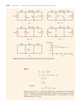
![we might call a free-body diagram of the right half of the network in Fig. 7.1a, as shown
in Fig. 7.1c (that is, a charged capacitor that is discharged through a resistor). When the
switch is closed, KCL for the circuit is
or
In the next section we will demonstrate that the solution of this equation is
Note that this function is a decaying exponential and the rate at which it decays is a function
of the values of R and C. The product RC is a very important parameter, and we will give it
a special name in the following discussions.
vC(t) = V
o e-t兾RC
dvC(t)
dt
+
1
RC
vC(t) = 0
C
dvC(t)
dt
+
vC(t)
R
= 0
298 C H A P T E R 7 F I R S T- A N D S E C O N D - O R D E R T R A N S I E N T C I R C U I T S
Discharge
time
Charge
time
Vo
(b)
vC(t)
t
RS
R
[(R) Xenon lamp]
VS
C
(a)
vC(t)
+
-
(c)
vC(t) R
C
+
-
Figure 7.1
Diagrams used to
describe a camera’s
flash circuit.
7.2
First-Order
Circuits
GENERAL FORM OF THE RESPONSE EQUATIONS In our study of first-order tran-
sient circuits we will show that the solution of these circuits (i.e., finding a voltage or cur-
rent) requires us to solve a first-order differential equation of the form
7.1
Although a number of techniques may be used for solving an equation of this type, we will
obtain a general solution that we will then employ in two different approaches to transient
analysis.
A fundamental theorem of differential equations states that if is any solution
to Eq. (7.1), and is any solution to the homogeneous equation
7.2
dx(t)
dt
+ ax(t) = 0
x(t) = xc(t)
x(t) = xp(t)
dx(t)
dt
+ ax(t) = f(t)
irwin07_296-368hr.qxd 28-07-2010 11:34 Page 298](https://image.slidesharecdn.com/basic-engineering-circuit-analysis-10th-irwin-220801002926-2b111212/85/basic-engineering-circuit-analysis-10th-Irwin-pdf-322-320.jpg)
![The Step-by-Step Approach In the previous analysis technique, we derived the differ-
ential equation for the capacitor voltage or inductor current, solved the differential equation,
and used the solution to find the unknown variable in the network. In the very methodical
technique that we will now describe, we will use the fact that Eq. (7.11) is the form of the
solution and we will employ circuit analysis to determine the constants and .
From Eq. (7.11) we note that as t S q, and Therefore, if the circuit
is solved for the variable x(t) in steady state (i.e., t S q) with the capacitor replaced by an
open circuit [v is constant and therefore ] or the inductor replaced by a
short circuit [i is constant and therefore ], then the variable
Note that since the capacitor or inductor has been removed, the circuit is a dc circuit with
constant sources and resistors, and therefore only dc analysis is required in the steady-state
solution.
The constant in Eq. (7.11) can also be obtained via the solution of a dc circuit in which
a capacitor is replaced by a voltage source or an inductor is replaced by a current source. The
value of the voltage source for the capacitor or the current source for the inductor is a known
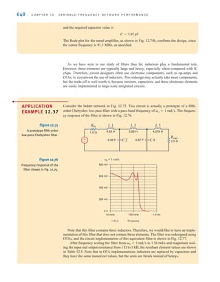
value at one instant of time. In general, we will use the initial condition value since it is gen-
erally the one known, but the value at any instant could be used. This value can be obtained
in numerous ways and is often specified as input data in a statement of the problem. However,
a more likely situation is one in which a switch is thrown in the circuit and the initial value
of the capacitor voltage or inductor current is determined from the previous circuit (i.e., the
circuit before the switch is thrown). It is normally assumed that the previous circuit has
reached steady state, and therefore the voltage across the capacitor or the current through the
inductor can be found in exactly the same manner as was used to find
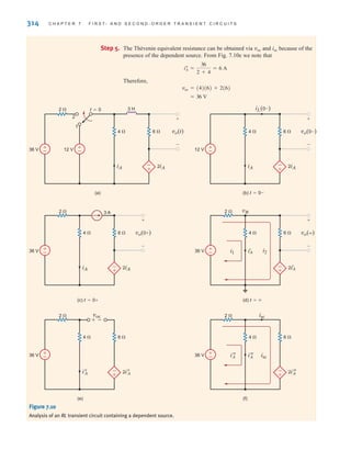
Finally, the value of the time constant can be found by determining the Thévenin equiva-
lent resistance at the terminals of the storage element. Then for an RC circuit, and
for an RL circuit.
Let us now reiterate this procedure in a step-by-step fashion.
= L兾RTh
= RThC
K1.
K2
x(t) = K1.
v = L(di兾dt) = 0
i = C(dv兾dt) = 0
x(t) = K1.
e-at
S 0
K1, K2,
306 C H A P T E R 7 F I R S T- A N D S E C O N D - O R D E R T R A N S I E N T C I R C U I T S
Step 1. We assume a solution for the variable x(t) of the form
Step 2. Assuming that the original circuit has reached steady state before a switch was
thrown (thereby producing a new circuit), draw this previous circuit with the
capacitor replaced by an open circuit or the inductor replaced by a short circuit.
Solve for the voltage across the capacitor, or the current through the
inductor, prior to switch action.
Step 3. Recall from Chapter 6 that voltage across a capacitor and the current flowing
through an inductor cannot change in zero time. Draw the circuit valid for
with the switches in their new positions. Replace a capacitor with a
voltage source or an inductor with a current source of value
Solve for the initial value of the variable
Step 4. Assuming that steady state has been reached after the switches are thrown,
draw the equivalent circuit, valid for by replacing the capacitor by
an open circuit or the inductor by a short circuit. Solve for the steady-state
value of the variable
Step 5. Since the time constant for all voltages and currents in the circuit will be the
same, it can be obtained by reducing the entire circuit to a simple series circuit
containing a voltage source, resistor, and a storage element (i.e., capacitor or
inductor) by forming a simple Thévenin equivalent circuit at the terminals of
x(t)|t75 ⬟ x(q)
t 7 5,
x(0+).
iL(0+) = iL(0-).
vC(0+) = vC(0-)
t = 0+
iL(0-),
vC(0-),
x(t) = K1 + K2e-t兾
.
Problem-Solving Strategy
Using the Step-by-
Step Approach
irwin07_296-368hr.qxd 28-07-2010 11:34 Page 306](https://image.slidesharecdn.com/basic-engineering-circuit-analysis-10th-irwin-220801002926-2b111212/85/basic-engineering-circuit-analysis-10th-Irwin-pdf-330-320.jpg)
![S E C T I O N 7 . 2 F I R S T- O R D E R C I R C U I T S 307
the storage element. This Thévenin equivalent circuit is obtained by looking
into the circuit from the terminals of the storage element. The time constant for
a circuit containing a capacitor is and for a circuit containing an
inductor it is
Step 6. Using the results of steps 3, 4, and 5, we can evaluate the constants in step 1 as
Therefore, and hence the solution is
Keep in mind that this solution form applies only to a first-order circuit having
dc sources. If the sources are not dc, the forced response will be different.
Generally, the forced response is of the same form as the forcing functions
(sources) and their derivatives.
x(t) = x(q) + [x(0+) - x(q)]e-t兾
K1 = x(q), K2 = x(0+) - x(q),
x(q) = K1
x(0+) = K1 + K2
= L兾RTh.
= RTh C,
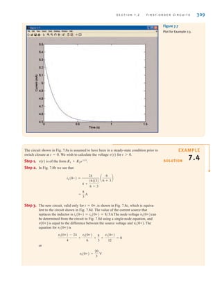
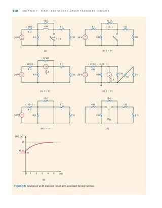
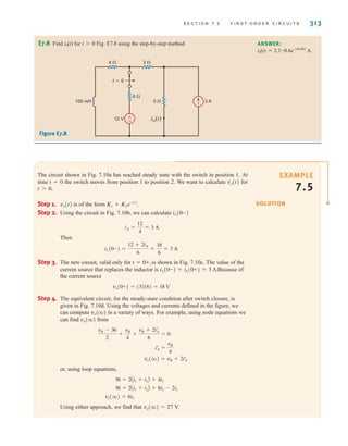
Consider the circuit shown in Fig. 7.6a. The circuit is in steady state prior to time t=0,
when the switch is closed. Let us calculate the current i(t) for
Step 1. i(t) is of the form
Step 2. The initial voltage across the capacitor is calculated from Fig. 7.6b as
Step 3. The new circuit, valid only for is shown in Fig. 7.6c. The value of the
voltage source that replaces the capacitor is Hence,
Step 4. The equivalent circuit, valid for is shown in Fig. 7.6d. The current i(q)
caused by the 36-V source is
Step 5. The Thévenin equivalent resistance, obtained by looking into the open-circuit
terminals of the capacitor in Fig. 7.6e, is
Therefore, the circuit time constant is
= 0.15 s
= a
3
2
b A103
B(100)A10-6
B
= RThC
RTh =
(2k)(6k)
2k + 6k
=
3
2
k⍀
=
9
2
mA
i(q) =
36
2k + 6k
t 7 5,
=
16
3
mA
i(0+) =
32
6k
vC(0-) = vC(0+) = 32 V.
t = 0+,
= 32 V
vC(0-) = 36 - (2)(2)
K1 + K2e-t兾
.
t 7 0.
SOLUTION
EXAMPLE
7.3
irwin07_296-368hr.qxd 28-07-2010 11:34 Page 307](https://image.slidesharecdn.com/basic-engineering-circuit-analysis-10th-irwin-220801002926-2b111212/85/basic-engineering-circuit-analysis-10th-Irwin-pdf-331-320.jpg)
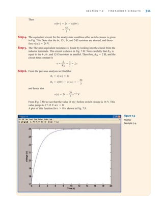
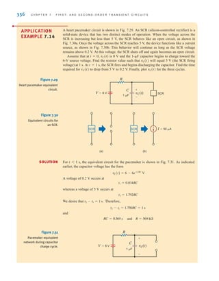
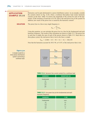
![S E C T I O N 7 . 5 D E S I G N E X A M P L E S 349
iL(t), we should reduce s1. Hence, let us choose s1=1. Since s1+s2 must equal 20,
s2=19. Under these conditions
and
Thus, the current is
which is shown in Fig. 7.51b. At 100 ms the current is 2.52 A. Also, at t=1.1 s, the cur-
rent is 1.11 A—above the 1-A requirement. Therefore, the choice of C=263 mF meets all
starter specifications.
iL(t) = 3.33Ce-t
- e-19t
D A
K1 =
60
s2 - s1
=
60
18
= 3.33
C =
1
Ls1s2
=
1
(0.2)(1)(19)
= 263 mF
A defibrillator is a device that is used to stop heart fibrillations—erratic uncoordinated
quivering of the heart muscle fibers—by delivering an electric shock to the heart. The Lown
defibrillator was developed by Dr. Bernard Lown in 1962. Its key feature, shown in Fig. 7.52a,
is its voltage waveform. A simplified circuit diagram that is capable of producing the Lown
waveform is shown in Fig. 7.52b. Let us find the necessary values for the inductor and
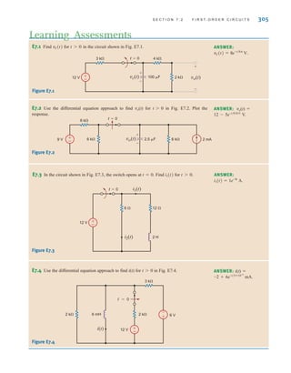
capacitor.
DESIGN
EXAMPLE 7.21
SOLUTION
(b)
3000
0 5 10
Time (milliseconds)
vo(t) (V)
(a)
vo(t)
VS
6000 V
R=50
patient
C
i(t)
L
t=0
+
-
Figure 7.52 Lown defibrillator waveform and simplified circuit. Reprinted with permission from John
Wiley Sons, Inc., Introduction to Biomedical Equipment Technology.
Since the Lown waveform is oscillatory in nature, we know that the circuit is underdamped
and the voltage applied to the patient is of the form
where
and
o =
1
1LC
= o 21 - 2
o =
R
2L
vo(t) = K1e-ot
sin[t]
( 6 1)
•
irwin07_296-368hr.qxd 28-07-2010 11:34 Page 349](https://image.slidesharecdn.com/basic-engineering-circuit-analysis-10th-irwin-220801002926-2b111212/85/basic-engineering-circuit-analysis-10th-Irwin-pdf-373-320.jpg)

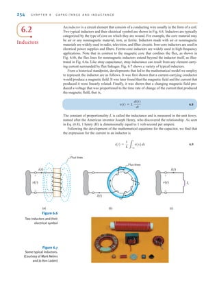
![8.1
Sinusoids
Let us begin our discussion of sinusoidal functions by considering the sine wave
8.1
where x(t) could represent either v(t) or i(t). XM is the amplitude, maximum value, or peak
value; is the radian or angular frequency; and t is the argument of the sine function. A
plot of the function in Eq. (8.1) as a function of its argument is shown in Fig. 8.1a. Obviously,
the function repeats itself every 2 radians. This condition is described mathematically as
, or in general for period T, as
8.2
meaning that the function has the same value at time t+T as it does at time t.
xC(t + T)D = x(t)
x(t + 2) = x(t)
x(t) = XM sint
370 C H A P T E R 8 A C S T E A D Y- S T A T E A N A LY S I S
The waveform can also be plotted as a function of time, as shown in Fig. 8.1b. Note that
this function goes through one period every T seconds. In other words, in 1 second it goes
through 1/T periods or cycles. The number of cycles per second, called Hertz, is the
frequency f, where
8.3
Now since as shown in Fig. 8.1a, we find that
8.4
which is, of course, the general relationship among period in seconds, frequency in Hertz,
and radian frequency.
Now that we have discussed some of the basic properties of a sine wave, let us consider
the following general expression for a sinusoidal function:
8.5
In this case is the argument of the sine function, and is called the phase angle.
A plot of this function is shown in Fig. 8.2, together with the original function in Eq. (8.1)
for comparison. Because of the presence of the phase angle, any point on the waveform
occurs radians earlier in time than the corresponding point on the wave-
form Therefore, we say that lags by radians. In the
more general situation, if
and
x2(t) = XM2
sin(t + )
x1(t) = XM1
sin(t + )
XM sin(t + )
XM sin t
XM sin t.
XM sin(t + )
(t + )
x(t) = XM sin(t + )
=
2
T
= 2f
T = 2,
f =
1
T
–XM
XM
–XM
XM
x(t)
—
2
——
2
3
2 t
(a)
x(t)
T
——
4
——
4
3T
T t
(b)
T
—
2
Figure 8.1
Plots of a sine wave as a
function of both and t.
t
The relationship between
frequency and period
[ h i n t ]
The relationship between
frequency, period, and radian
frequency
[ h i n t ]
Phase lag defined
[ h i n t ]
In phase and out of phase
defined
[ h i n t ]
irwin08_369-434hr.qxd 28-07-2010 12:03 Page 370](https://image.slidesharecdn.com/basic-engineering-circuit-analysis-10th-irwin-220801002926-2b111212/85/basic-engineering-circuit-analysis-10th-Irwin-pdf-394-320.jpg)
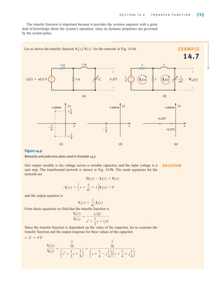
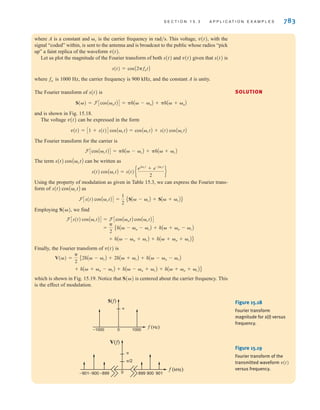
![S E C T I O N 8 . 1 S I N U S O I D S 371
then leads by - radians and lags by - radians. If =, the
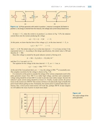
waveforms are identical and the functions are said to be in phase. If the functions are
out of phase.
The phase angle is normally expressed in degrees rather than radians. Therefore, at this
point we will simply state that we will use the two forms interchangeably; that is,
8.6
Rigorously speaking, since t is in radians, the phase angle should be as well. However, it is
common practice and convenient to use degrees for phase; therefore, that will be our practice
in this text.
In addition, it should be noted that adding to the argument integer multiples of either 2
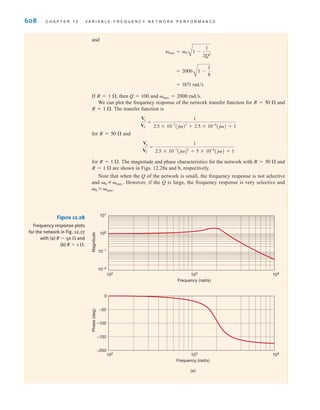
radians or 360° does not change the original function. This can easily be shown mathemati-
cally but is visibly evident when examining the waveform, as shown in Fig. 8.2.
Although our discussion has centered on the sine function, we could just as easily have
used the cosine function, since the two waveforms differ only by a phase angle; that is,
8.7
8.8
We are often interested in the phase difference between two sinusoidal functions. Three
conditions must be satisfied before we can determine the phase difference: (1) the
frequency of both sinusoids must be the same, (2) the amplitude of both sinusoids must be
positive, and (3) both sinusoids must be written as sine waves or cosine waves. Once
in this format, the phase angle between the functions can be computed as outlined
previously. Two other trigonometric identities that normally prove useful in phase angle
determination are
8.9
8.10
Finally, the angle-sum and angle-difference relationships for sines and cosines may be
useful in the manipulation of sinusoidal functions. These relations are
8.11
cos( - ) = cos cos + sin sin
sin( - ) = sin cos - cos sin
cos( + ) = cos cos - sin sin
sin( + ) = sin cos + cos sin
-sin(t) = sin(t ; 180°)
-cos(t) = cos(t ; 180°)
sint = cos at -
2
b
cost = sin at +
2
b
x(t) = XM sin at +
2
b = XM sin(t + 90°)
Z ,
x1(t)
x2(t)
x2(t)
x1(t)
x(t)
2 t
XM sin (t+)
XM sin t
Figure 8.2
Graphical illustration of
leading
by radians.
XM sint
XM sin˚(t + )
Phase lead graphically
illustrated
[ h i n t ]
A very important point
[ h i n t ]
Some trigonometric identities
that are useful in phase angle
calculations
[ h i n t ]
irwin08_369-434hr.qxd 28-07-2010 12:03 Page 371](https://image.slidesharecdn.com/basic-engineering-circuit-analysis-10th-irwin-220801002926-2b111212/85/basic-engineering-circuit-analysis-10th-Irwin-pdf-395-320.jpg)
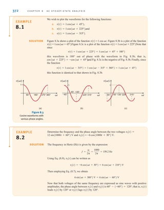
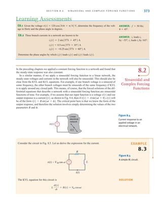
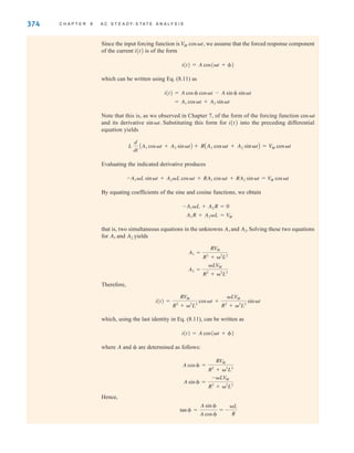
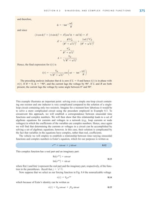
![376 C H A P T E R 8 A C S T E A D Y- S T A T E A N A LY S I S
The real and imaginary parts of this function are each realizable. We think of this complex
forcing function as two forcing functions, a real one and an imaginary one, and as a consequence
of linearity, the principle of superposition applies and thus the current response can be written as
8.16
where is the response due to and is the response
due to This expression for the current containing both a real and an imaginary
term can be written via Euler’s equation as
8.17
Because of the preceding relationships, we find that rather than apply the forcing function
and calculate the response we can apply the complex forcing
function and calculate the response the real part of which is the desired
response Although this procedure may initially appear to be more compli-
cated, it is not. It is through this technique that we will convert the differential equation to an
algebraic equation that is much easier to solve.
IM cos(t + ).
IMej(t+)
,
V
Mejt
IM cos(t + ),
V
M cost
i(t) = IMej(t+)
jV
M sint.
jIM sin(t + )
V
M cost
IM cos(t + )
i(t) = IM cos(t + ) + jIM sin(t + )
Once again, let us determine the current in the RL circuit examined in Example 8.3.
However, rather than apply , we will apply
The forced response will be of the form
where only and are unknown. Substituting v(t) and i(t) into the differential equation
for the circuit, we obtain
Taking the indicated derivative, we obtain
Dividing each term of the equation by the common factor yields
which is an algebraic equation with complex coefficients. This equation can be written as
Converting the right-hand side of the equation to exponential or polar form produces the
equation
(A quick refresher on complex numbers is given in the Appendix for readers who need to
sharpen their skills in this area.) The preceding form clearly indicates that the magnitude
and phase of the resulting current are
and
= -tan-1 L
R
IM =
V
M
2R2
+ 2
L2
IMej
=
V
M
2R2
+ 2
L2
ejC-tan-1
(L兾R)D
IMej
=
V
M
R + jL
RIMej
+ jLIMej
= V
M
ejt
RIMej(t+)
+ jLIMej(t+)
= V
Mejt
RIMej(t+)
+ L
d
dt
AIMej(t+)
B = V
Mejt
IM
i(t) = IMej(t+)
V
Mejt
.
VM cost
EXAMPLE
8.4 SOLUTION
Summary of complex number
relationships:
1
ej
= e-j
y = r sin
x = r cos
= tan-1
y
x
r = 2x2
+ y2
x + jy = rej
[ h i n t ]
irwin08_369-434hr.qxd 28-07-2010 12:03 Page 376](https://image.slidesharecdn.com/basic-engineering-circuit-analysis-10th-irwin-220801002926-2b111212/85/basic-engineering-circuit-analysis-10th-Irwin-pdf-400-320.jpg)
![S E C T I O N 8 . 3 P H A S O R S 377
However, since our actual forcing function was rather than our actual
response is the real part of the complex response:
Note that this is identical to the response obtained in the previous example by solving the
differential equation for the current i(t).
=
V
M
2R2
+ 2
L2
cos at - tan-1 L
R
b
i(t) = IM cos(t + )
V
Mejt
,
V
M cost
8.3
Phasors
Once again let us assume that the forcing function for a linear network is of the form
Then every steady-state voltage or current in the network will have the same form and the
same frequency ; for example, a current i(t) will be of the form
As we proceed in our subsequent circuit analyses, we will simply note the frequency and
then drop the factor since it is common to every term in the describing equations.
Dropping the term indicates that every voltage or current can be fully described by a mag-
nitude and phase. For example, a voltage v(t) can be written in exponential form as
8.18
or as a complex number
8.19
Since we are working with a complex forcing function, the real part of which is the
desired answer, and each term in the equation will contain we can drop Re(ⴢ) and
and work only with the complex number This complex representation is commonly
called a phasor. As a distinguishing feature, phasors will be written in boldface type. In
a completely identical manner a voltage and a
current = are written in phasor notation as
and respectively. Note that it is common practice to express pha-
sors with positive magnitudes.
I = IM /,
V = V
M /
ReCIMej(t+)
D
i(t) = IM cos (t + )
v(t) = V
M cos(t + ) = ReCV
Mej(t+)
D
V
M /.
ejt
ejt
,
v(t) = ReAV
M / ejt
B
v(t) = V
M cos(t + ) = ReCV
Mej(t+)
D
ejt
ejt
i(t) = IMej(t+)
.
v(t) = V
Mejt
If and
, then
in phasor notation
and
I = IM /
V = VM /
i(t) = IM cos(t + )
v(t) = VM cos(t + )
[ h i n t ]
Again, we consider the RL circuit in Example 8.3. Let us use phasors to determine the
expression for the current.
The differential equation is
The forcing function can be replaced by a complex forcing function that is written as
with phasor Similarly, the forced response component of the current
i(t) can be replaced by a complex function that is written as with phasor
From our previous discussions we recall that the solution of the differential equation is
the real part of this current.
I = IM /.
Iejt
V = V
M /0°.
Vejt
L
di(t)
dt
+ Ri(t) = VM cost
SOLUTION
EXAMPLE
8.5
irwin08_369-434hr.qxd 28-07-2010 12:03 Page 377](https://image.slidesharecdn.com/basic-engineering-circuit-analysis-10th-irwin-220801002926-2b111212/85/basic-engineering-circuit-analysis-10th-Irwin-pdf-401-320.jpg)
![378 C H A P T E R 8 A C S T E A D Y- S T A T E A N A LY S I S
Using the complex forcing function, we find that the differential equation becomes
Note that is a common factor and, as we have already indicated, can be eliminated, leaving
the phasors; that is,
Therefore,
Thus,
which once again is the function we obtained earlier.
i(t) =
VM
2R2
+ 2
L2
cos at - tan-1 L
R
b
I =
V
R + jL
= IM / =
V
M
2R2
+ 2
L2 ^-tan-1 L
R
jLI + RI = V
ejt
jLIejt
+ RIejt
= Vejt
L
d
dt
AIejt
B + RIejt
= Vejt
The differential equation is
reduced to a phasor equation.
[ h i n t ]
We define relations between phasors after the term has been eliminated as “phasor, or
frequency domain, analysis.” Thus, we have transformed a set of differential equations with
sinusoidal forcing functions in the time domain into a set of algebraic equations containing
complex numbers in the frequency domain. In effect, we are now faced with solving a set of
algebraic equations for the unknown phasors. The phasors are then simply
transformed back to the time domain to yield the solution of the original set of differential
equations. In addition, we note that the solution of sinusoidal steady-state circuits would be
relatively simple if we could write the phasor equation directly from the circuit description.
In Section 8.4 we will lay the groundwork for doing just that.
Note that in our discussions we have tacitly assumed that sinusoidal functions would be rep-
resented as phasors with a phase angle based on a cosine function. Therefore, if sine functions
are used, we will simply employ the relationship in Eq. (8.7) to obtain the proper phase angle.
In summary, while v(t) represents a voltage in the time domain, the phasor V represents
the voltage in the frequency domain. The phasor contains only magnitude and phase infor-
mation, and the frequency is implicit in this representation. The transformation from the time
domain to the frequency domain, as well as the reverse transformation, is shown in Table 8.1.
Recall that the phase angle is based on a cosine function and, therefore, if a sine function is
involved, a 90° shift factor must be employed, as shown in the table.
ejt
TABLE 8.1 Phasor representation
A/; - 90°
A sin(t ; )
A/;
A cos(t ; )
Step 1. Using phasors, transform a set of differential equations in the time domain into
a set of algebraic equations in the frequency domain.
Step 2. Solve the algebraic equations for the unknown phasors.
Step 3. Transform the now-known phasors back to the time domain.
Phasor Analysis
Problem-Solving Strategy
TIME DOMAIN FREQUENCY DOMAIN
irwin08_369-434hr.qxd 28-07-2010 12:03 Page 378](https://image.slidesharecdn.com/basic-engineering-circuit-analysis-10th-irwin-220801002926-2b111212/85/basic-engineering-circuit-analysis-10th-Irwin-pdf-402-320.jpg)
![S E C T I O N 8 . 4 P H A S O R R E L A T I O N S H I P S F O R C I R C U I T E L E M E N T S 379
E8.3 Convert the following voltage functions to phasors.
v2(t) = 18 sin(2513t + 4.2°) V
v1(t) = 12 cos(377t - 425°) V
Learning Assessments
ANSWER:
V2 = 18/-85.8° V.
V1 = 12/-425° V;
E8.4 Convert the following phasors to the time domain if the frequency is 400 Hz.
V2 = 12/-60° V
V1 = 10/20° V
ANSWER:
v2(t) = 12 cos(800t - 60°) V.
v1(t) = 10 cos(800t + 20°) V;
However, if a network contains only sine sources, there is no need to perform the 90° shift.
We simply perform the normal phasor analysis, and then the imaginary part of the time-
varying complex solution is the desired response. Simply put, cosine sources generate a
cosine response, and sine sources generate a sine response.
As we proceed in our development of the techniques required to analyze circuits in the sinu-
soidal steady state, we are now in a position to establish the phasor relationships between
voltage and current for the three passive elements R, L, and C.
In the case of a resistor as shown in Fig. 8.6a, the voltage–current relationship is known to be
8.20
Applying the complex voltage results in the complex current and there-
fore Eq. (8.20) becomes
which reduces to
8.21
Equation (8.21) can be written in phasor form as
8.22
where
From Eq. (8.21) we see that and thus the current and voltage for this circuit are in phase.
Historically, complex numbers have been represented as points on a graph in which the
x-axis represents the real axis and the y-axis the imaginary axis. The line segment connect-
ing the origin with the point provides a convenient representation of the magnitude and angle
when the complex number is written in a polar form. A review of the Appendix will indicate
how these complex numbers or line segments can be added, subtracted, and so on. Since
phasors are complex numbers, it is convenient to represent the phasor voltage and current
graphically as line segments. A plot of the line segments representing the phasors is called a
phasor diagram. This pictorial representation of phasors provides immediate information on
the relative magnitude of one phasor with another, the angle between two phasors, and the
relative position of one phasor with respect to another (i.e., leading or lagging). A phasor
diagram and the sinusoidal waveforms for the resistor are shown in Figs. 8.6c and d, res-
pectively. A phasor diagram will be drawn for each of the other circuit elements in the
remainder of this section.
v = i
V = V
Mejv
= V
M /v and I = IMeji
= IM/i
V = RI
V
Mejv
= RIMeji
V
MejAt+vB
= RIMejAt+iB
IMejAt+iB
,
V
MejAt+vB
v(t) = Ri(t)
8.4
Phasor
Relationships for
Circuit Elements
Current and voltage are in
phase.
[ h i n t ]
irwin08_369-434hr.qxd 28-07-2010 12:03 Page 379](https://image.slidesharecdn.com/basic-engineering-circuit-analysis-10th-irwin-220801002926-2b111212/85/basic-engineering-circuit-analysis-10th-Irwin-pdf-403-320.jpg)
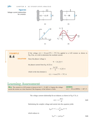
![S E C T I O N 8 . 4 P H A S O R R E L A T I O N S H I P S F O R C I R C U I T E L E M E N T S 381
The voltage is applied to a 20-mH inductor as shown in
Fig. 8.7a. Find the resultant current.
The phasor current is
or
i(t) = 1.59 cos(377t - 70°) A
= 1.59/-70° A
=
12/20°
(377)(20 * 10-3
)/90°
I =
V
jL
=
12/20°
L/90°
v(t) = 12 cos(377t + 20°) V
SOLUTION
EXAMPLE
8.7
Figure 8.7
Voltage–current relationships
for an inductor.
(a) (b)
(c) (d)
v(t), i(t)
t
v(t) i(t)
Im
Re
I
v=i +90°
i
90°
V
v(t)=L
di(t)
dt
–––
i(t)
L
+
-
V=jLI
I
+
-
L
Equation (8.24) in phasor notation is
8.25
Note that the differential equation in the time domain (8.23) has been converted to an alge-
braic equation with complex coefficients in the frequency domain. This relationship is
shown in Fig. 8.7b. Since the imaginary operator , Eq. (8.24)
can be written as
8.26
Therefore, the voltage and current are 90° out of phase, and in particular the voltage leads the
current by 90° or the current lags the voltage by 90°. The phasor diagram and the sinusoidal
waveforms for the inductor circuit are shown in Figs. 8.7c and d, respectively.
V
Mejv
= LIMejAi +90°B
j = 1ej90°
= 1/90° = 1-1
V = jLI
The derivative process yields
a frequency-dependent
function.
[ h i n t ]
The voltage leads the current
or the current lags the
voltage.
[ h i n t ]
Applying
x1 /1
x2 /2
=
x1
x2
/1 - 2
V = jLI
[ h i n t ]
irwin08_369-434hr.qxd 28-07-2010 12:03 Page 381](https://image.slidesharecdn.com/basic-engineering-circuit-analysis-10th-irwin-220801002926-2b111212/85/basic-engineering-circuit-analysis-10th-Irwin-pdf-405-320.jpg)
![382 C H A P T E R 8 A C S T E A D Y- S T A T E A N A LY S I S
E8.6 The current in a 0.05-H inductor is If the frequency of the cur-
rent is 60 Hz, determine the voltage across the inductor.
I = 4/-30° A.
Learning Assessment
The voltage–current relationship for our last passive element, the capacitor, as shown in
Fig. 8.8a, is
8.27
Once again employing the complex voltage and current, we obtain
which reduces to
8.28
In phasor notation this equation becomes
8.29
Eq. (8.27), a differential equation in the time domain, has been transformed into Eq. (8.29),
an algebraic equation with complex coefficients in the frequency domain. The phasor rela-
tionship is shown in Fig. 8.8b. Substituting into Eq. (8.28) yields
8.30
Note that the voltage and current are 90° out of phase. Eq. (8.30) states that the current
leads the voltage by 90° or the voltage lags the current by 90°. The phasor diagram and the
sinusoidal waveforms for the capacitor circuit are shown in Figs. 8.8c and d, respectively.
IMeji
= CV
MejAv +90°B
j = 1ej90°
I = jCV
IMeji
= jCV
Mejv
IMejAt+iB
= C
d
dt
V
MejAt+vB
i(t) = C
dv(t)
dt
Figure 8.8
Voltage–current relationships
for a capacitor.
90°
(a) (b)
(c) (d)
i=v +90°
Im
Re
V
v
I
v(t)
i(t)
v(t), i(t)
t
v(t)
i(t)=C
dv(t)
dt
–––
C
+
-
V
I=jCV
+
-
C
The current leads the voltage
or the voltage lags the
current.
[ h i n t ]
ANSWER:
vL(t) = 75.4 cos(377t + 60°) V.
irwin08_369-434hr.qxd 28-07-2010 12:03 Page 382](https://image.slidesharecdn.com/basic-engineering-circuit-analysis-10th-irwin-220801002926-2b111212/85/basic-engineering-circuit-analysis-10th-Irwin-pdf-406-320.jpg)
![8.5
Impedance and
Admittance
We have examined each of the circuit elements in the frequency domain on an individual
basis. We now wish to treat these passive circuit elements in a more general fashion. We
define the two-terminal input impedance Z, also referred to as the driving point impedance,
in exactly the same manner in which we defined resistance earlier. Later we will examine
another type of impedance, called transfer impedance.
Impedance is defined as the ratio of the phasor voltage V to the phasor current I:
8.31
at the two terminals of the element related to one another by the passive sign convention, as
illustrated in Fig. 8.9. Since V and I are complex, the impedance Z is complex and
8.32
Since Z is the ratio of V to I, the units of Z are ohms. Thus, impedance in an ac circuit is
analogous to resistance in a dc circuit. In rectangular form, impedance is expressed as
8.33
where is the real, or resistive, component and is the imaginary, or reactive,
component. In general, we simply refer to R as the resistance and X as the reactance. It is
X()
R()
Z() = R() + jX()
Z =
V
M /v
IM /i
=
V
M
IM
/v - i = Z/z
Z =
V
I
S E C T I O N 8 . 5 I M P E D A N C E A N D A D M I T T A N C E 383
The voltage is applied to a 100- F capacitor as shown in
Fig. 8.8a. Find the current.
The resultant phasor current is
Therefore, the current written as a time function is
i(t) = 3.14 cos(314t + 105°) A
= 3.14/105° A
= (314)A100 * 10-6
/90°BA100/15°B
I = jCA100/15° B
v(t) = 100 cos(314t + 15°) V
SOLUTION
EXAMPLE
8.8
Applying I = jCV
[ h i n t ]
E8.7 The current in a 150- F capacitor is If the frequency of the
current is 60 Hz, determine the voltage across the capacitor.
I = 3.6/-145° A.
Learning Assessment
ANSWER:
.
vC(t) = 63.66 cos(377t - 235°) V
±
– Z z
IM i
VM v
ac
circuit
Figure 8.9
General impedance
relationship.
irwin08_369-434hr.qxd 28-07-2010 12:03 Page 383](https://image.slidesharecdn.com/basic-engineering-circuit-analysis-10th-irwin-220801002926-2b111212/85/basic-engineering-circuit-analysis-10th-Irwin-pdf-407-320.jpg)
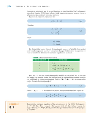
![386 C H A P T E R 8 A C S T E A D Y- S T A T E A N A LY S I S
E8.8 Find the current i(t) in the network in Fig. E8.8.
Learning Assessment
ANSWER:
i(t) = 3.88 cos(377t - 39.2°) A.
±
–
v(t)=120 sin
(377t+60°) V
i(t)
40 mH
20
50 F
Figure E8.8
Technique for taking the
reciprocal:
=
R - jX
R2
+ X2
1
R + jX
=
R - jX
(R + jX)(R - jX)
[ h i n t ]
Another quantity that is very useful in the analysis of ac circuits is the two-terminal input
admittance, which is the reciprocal of impedance; that is,
8.38
The units of Y are siemens, and this quantity is analogous to conductance in resistive dc
circuits. Since Z is a complex number, Y is also a complex number.
8.39
which is written in rectangular form as
8.40
where G and B are called conductance and susceptance, respectively. Because of the relation-
ship between Y and Z, we can express the components of one quantity as a function of the
components of the other. From the expression
8.41
we can show that
8.42
and in a similar manner, we can show that
8.43
It is very important to note that in general R and G are not reciprocals of one another. The
same is true for X and B. The purely resistive case is an exception. In the purely reactive case,
the quantities are negative reciprocals of one another.
The admittance of the individual passive elements are
8.44
YC = jC = C/90°
YL =
1
jL
= -
1
L
/90°
YR =
1
R
= G
R =
G
G2
+ B2
, X =
-B
G2
+ B2
G =
R
R2
+ X2
, B =
-X
R2
+ X2
G + jB =
1
R + jX
Y = G + jB
Y = Y
M /y
Y =
1
Z
=
I
V
irwin08_369-434hr.qxd 28-07-2010 12:03 Page 386](https://image.slidesharecdn.com/basic-engineering-circuit-analysis-10th-irwin-220801002926-2b111212/85/basic-engineering-circuit-analysis-10th-Irwin-pdf-410-320.jpg)
![S E C T I O N 8 . 5 I M P E D A N C E A N D A D M I T T A N C E 387
Calculate the equivalent admittance for the network in Fig. 8.11 and use it to determine
the current I if VS = 60/45° V.
Yp
SOLUTION
EXAMPLE
8.10
Once again, since KCL and KVL are valid in the frequency domain, we can show, using
the same approach outlined in Chapter 2 for conductance in resistive circuits, that the rules
for combining admittances are the same as those for combining conductances; that is, if
are connected in parallel, the equivalent admittance is
8.45
and if are connected in series, the equivalent admittance is
8.46
1
YS
=
1
Y1
+
1
Y2
+ p +
1
Yn
Y1, Y2, p , Yn
Yp = Y1 + Y2 + p + Yn
Y1, Y2, Y3, p , Yn
Figure 8.11
Example parallel
circuit.
±
–
VS Yp ZR=2 ZL=j4
I
From Fig. 8.11 we note that
Therefore,
and hence,
= 33.5/18.43° A
= a
1
2
- j
1
4
b A60/45°B
I = YpVS
Yp =
1
2
- j
1
4
S
YL =
1
ZL
=
-j
4
S
YR =
1
ZR
=
1
2
S
Admittances add in
parallel.
[ h i n t ]
E8.9 Find the current I in the network in Fig. E8.9.
Learning Assessments
ANSWER: I = 9.01/53.7°A.
±
– ZR=2 ZR=4
ZL=j2 ZC=–j1
I
V=10 20° V
Figure E8.9
irwin08_369-434hr.qxd 28-07-2010 12:03 Page 387](https://image.slidesharecdn.com/basic-engineering-circuit-analysis-10th-irwin-220801002926-2b111212/85/basic-engineering-circuit-analysis-10th-Irwin-pdf-411-320.jpg)
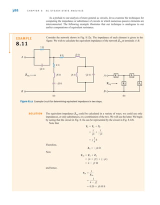
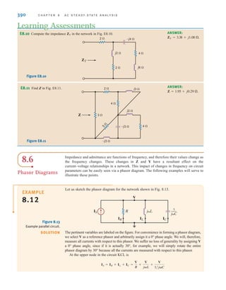
![S E C T I O N 8 . 6 P H A S O R D I A G R A M S 391
Since then
The phasor diagram that illustrates the phase relationship between V, IR , IL and IC is shown
in Fig. 8.14a. For small values of such that the magnitude of IL is greater than that of IC,
the phasor diagram for the currents is shown in Fig. 8.14b. In the case of large values of
—that is, those for which IC is greater than IL—the phasor diagram for the currents is
shown in Fig. 8.14c. Note that as increases, the phasor moves from to along a
locus of points specified by the dashed line shown in Fig. 8.14d.
Note that is in phase with V when or, in other words, when L=1/C.
Hence, the node voltage V is in phase with the current source when
This can also be seen from the KCL equation
I = c
1
R
+ jaC -
1
L
b dV
=
1
1LC
IS
IC = IL
IS
ISn
IS1
IS
IS =
V
M /0°
R
+
V
M /-90°
L
+ V
MC/90°
V = V
M /0°,
Figure 8.14
Phasor diagrams for the
circuit in Fig. 8.13.
(c) (d)
(a) (b)
V
IC
IL
IR
V
ISn
ISf
IS2
IS1
IR
V
IC
IL
IC+IL
IS
IR
V
IC
IL
IR
IS
IL+IC
From a graphical standpoint,
phasors can be manipulated
like vectors.
[ h i n t ]
Let us determine the phasor diagram for the series circuit shown in Fig. 8.15a.
KVL for this circuit is of the form
= IR + LI/90° +
I
C
/-90°
VS = VR + VL + VC
SOLUTION
EXAMPLE
8.13
irwin08_369-434hr.qxd 28-07-2010 12:03 Page 391](https://image.slidesharecdn.com/basic-engineering-circuit-analysis-10th-irwin-220801002926-2b111212/85/basic-engineering-circuit-analysis-10th-Irwin-pdf-415-320.jpg)
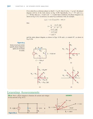
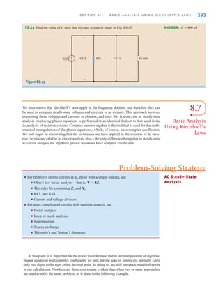
![394 C H A P T E R 8 A C S T E A D Y- S T A T E A N A LY S I S
We wish to calculate all the voltages and currents in the circuit shown in Fig. 8.16a.
Our approach will be as follows. We will calculate the total impedance seen by the source
Then we will use this to determine Knowing we can compute using KVL.
Knowing we can compute and and so on.
The total impedance seen by the source is
= 9.61/30.94°
= 4 + 4.24 + j4.94
= 4 +
24 + j48
8 + j2
Zeq = 4 +
(j6)(8 - j4)
j6 + 8 - j4
VS
I3,
I2
V1,
V1
I1,
I1.
VS.
Technique
1. Compute
2. Determine
Then and
Current and voltage
division are also applicable.
I3 =
V1
Z3
I2 =
V1
Z2
V1 = Vs - I1Z1
I1.
[ h i n t ]
I1
I1
V1
VS
VS
I2 I3
+
-
±
–
±
–
Z1
Z2 Z3
Figure 8.16 (a) Example ac circuit, (b) phasor diagram for the currents
(plots are not drawn to scale).
V2
+
-
V1
+
-
I1 I3
I2
±
–
I3
I1
I2
(b)
(a)
29.06°
–11.58°
105°
VS=24 60° V
4 8
j6 –j4
Then
can be determined using KVL:
Note that could also be computed via voltage division:
which from our previous calculation is
V1 =
VS
(j6)(8 - j4)
j6 + 8 - j4
4 +
(j6)(8 - j4)
j6 + 8 - 4
V
V1
= 16.26/78.43° V
= 3.26 + j15.93
= 24/60° - 10/29.06°
V1 = VS - 4I1
V1
= 2.5/29.06° A
I1 =
VS
Zeq
=
24/60°
9.61/30.94°
EXAMPLE
8.14 SOLUTION
irwin08_369-434hr.qxd 28-07-2010 12:03 Page 394](https://image.slidesharecdn.com/basic-engineering-circuit-analysis-10th-irwin-220801002926-2b111212/85/basic-engineering-circuit-analysis-10th-Irwin-pdf-418-320.jpg)
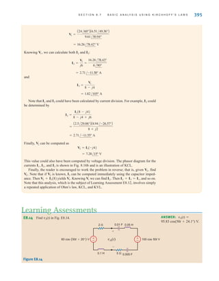
![396 C H A P T E R 8 A C S T E A D Y- S T A T E A N A LY S I S
E8.15 Find in Fig. E8.15.
Vo
ANSWER:
Vo = 2.98/-153.43° V.
Figure E8.15
Figure E8.16
E8.16 In the network in Fig. E8.16, is known to be Compute .
VS
8/45° V.
Vo ANSWER:
VS = 17.89/-18.43° V.
±
–
VS V1
I2
I3
I1
2
2
j2 Vo
–j2 +
+
-
-
In this section we revisit the circuit analysis methods that were successfully applied earlier
to dc circuits and illustrate their applicability to ac steady-state analysis. The vehicle we
employ to present these techniques is examples in which all the theorems, together with
nodal analysis and loop analysis, are used to obtain a solution.
Let us determine the current in the network in Fig. 8.17a using nodal analysis, loop analy-
sis, superposition, source exchange, Thévenin’s theorem, and Norton’s theorem.
1. Nodal Analysis We begin with a nodal analysis of the network. The KCL equation
for the supernode that includes the voltage source is
V1
1 + j
- 2/0° +
V2
1
+
V2
1 - j
= 0
Io
EXAMPLE
8.15
8.8
Analysis
Techniques
SOLUTION
Summing the current, leaving
the supernode. Outbound
currents have a positive sign.
[ h i n t ]
4 2
Vo
+
-
–j 2
–j 2 j 2
2 0° A
irwin08_369-434hr.qxd 28-07-2010 12:03 Page 396](https://image.slidesharecdn.com/basic-engineering-circuit-analysis-10th-irwin-220801002926-2b111212/85/basic-engineering-circuit-analysis-10th-Irwin-pdf-420-320.jpg)
![S E C T I O N 8 . 8 A N A LY S I S T E C H N I Q U E S 397
and the associated KVL constraint equation is
Solving for in the second equation and using this value in the first equation yields
or
Solving for we obtain
Therefore,
2. Loop Analysis The network in Fig. 8.17b is used to perform a loop analysis. Note
that one loop current is selected that passes through the independent current source.
The three loop equations are
Combining the first two equations yields
The third loop equation can be simplified to the form
Solving this last equation for and substituting the value into the previous equa-
tion yields
or
I3 =
-10 + 6j
4
I3 c
-4 + 2j
1 - j
+ 1 - jd = 8 + 2j
I2
I2(1 - j) + I3(2 - j) = 0
I2(2) + I3(1 - j) = 8 + 2j
1I3 + 1AI2 + I3B - j1AI2 + I3B = 0
1AI1 + I2B + j1AI1 + I2B - 6/0° + 1AI2 + I3B - j1AI2 + I3B = 0
I1 = -2/0°
Io =
4 + j
1 + j
= a
5
2
-
3
2
jb A
V2 = a
4 + j
1 + j
b V
V2,
V2 c
1
1 + j
+ 1 +
1
1 - j
d =
6 + 2 + 2j
1 + j
V2 - 6/0°
1 + j
- 2/0° + V2 +
V2
1 - j
= 0
V1
V1 + 6/0° = V2
Figure 8.17 Circuits used
in Example 8.15 for node
and loop analysis.
+
-
j1
–j1
1
1
V1 V2
Io
1
2 0° A
6 0° V
+
-
j1
–j1
1
1
Io
I3
I2
1
2 0° A
6 0° V
I1
(b)
(a)
Just as in a dc analysis, the
loop equations assume that a
decrease in potential level
is
and an increase is .
[ h i n t ]
irwin08_369-434hr.qxd 28-07-2010 12:03 Page 397](https://image.slidesharecdn.com/basic-engineering-circuit-analysis-10th-irwin-220801002926-2b111212/85/basic-engineering-circuit-analysis-10th-Irwin-pdf-421-320.jpg)
![398 C H A P T E R 8 A C S T E A D Y- S T A T E A N A LY S I S
Figure 8.18
Circuits used in Example
8.15 for a superposition
analysis.
j1
–j1
1
1
I'
o
1
2 0° A 2 0° A
(a)
1
I'
o
Z'
(b)
j1
–j1
1
1
I
o
V
1
1
6 0° V
+
-
+
-
(c)
and finally
3. Superposition In using superposition, we apply one independent source at a time.
The network in which the current source acts alone is shown in Fig. 8.18a. By combining
the two parallel impedances on each end of the network, we obtain the circuit in
Fig. 8.18b, where
Therefore, using current division,
The circuit in which the voltage source acts alone is shown in Fig. 8.18c. The voltage
obtained using voltage division is
and hence,
Then
4. Source Exchange As a first step in the source exchange approach, we exchange the
current source and parallel impedance for a voltage source in series with the imped-
ance, as shown in Fig. 8.19a.
Io = Iœ
o + Ifl
o = 1 +
6
4
(1 - j) = a
5
2
-
3
2
jb A
Ifl
0 =
6
4
(1 - j) A
=
6(1 - j)
4
V
Vfl
1 =
(6/0°)c
1(1 - j)
1 + 1 - j
d
1 + j + c
1(1 - j)
1 + 1 - j
d
Vfl
1
Iœ
o = 1/0° A
Z¿ =
(1 + j)(1 - j)
(1 + j) + (1 - j)
= 1
Io = -I3 = a
5
2
-
3
2
jb A
In applying superposition in
this case, each source is
applied independently, and
the results are added to
obtain the solution.
[ h i n t ]
irwin08_369-434hr.qxd 28-07-2010 12:03 Page 398](https://image.slidesharecdn.com/basic-engineering-circuit-analysis-10th-irwin-220801002926-2b111212/85/basic-engineering-circuit-analysis-10th-Irwin-pdf-422-320.jpg)
![S E C T I O N 8 . 8 A N A LY S I S T E C H N I Q U E S 399
j1
1
–j1
2(1+j) V 1
Io
1
6 0° V
+
-
(a)
±
–
–j1
(b)
1
1
1
j1
Io
6+2(1+j)
1+j
— A
c c
1
Io
Z
(c)
— A
8+2j
1+j
c c
Figure 8.19
Circuits used in
Example 8.15
for a source
exchange
analysis.
In source exchange, a voltage
source in series with an
impedance can be exchanged
for a current source in parallel
with the impedance and vice
versa. Repeated application
systematically reduces the
number of circuit elements.
[ h i n t ]
In this Thévenin analysis,
1. Remove the 1- load and
find the voltage across the
open terminals, .
2. Determine the impedance
ZTh at the open terminals
with all sources made zero.
3. Construct the following
circuit and determine .
Io
Voc
[ h i n t ]
±
–
ZTh
Voc 1
Io
Adding the two voltage sources and transforming them and the series impedance
into a current source in parallel with that impedance are shown in Fig. 8.19b.
Combining the two impedances that are in parallel with the 1- resistor produces
the network in Fig. 8.19c, where
Therefore, using current division,
5. Thévenin Analysis In applying Thévenin’s theorem to the circuit in Fig. 8.17a, we
first find the open-circuit voltage, as shown in Fig. 8.20a. To simplify the analysis,
we perform a source exchange on the left end of the network, which results in the
circuit in Fig. 8.20b. Now using voltage division,
or
The Thévenin equivalent impedance, obtained at the open-circuit terminals when
the current source is replaced with an open circuit and the voltage source is replaced
with a short circuit is shown in Fig. 8.20c and calculated to be
ZTh =
(1 + j)(1 - j)
1 + j + 1 - j
= 1
ZTh,
Voc = (5 - 3j) V
Voc = [6 + 2(1 + j)]c
1 - j
1 - j + 1 + j
d
Voc,
= a
5
2
-
3
2
jb A
Io = a
8 + 2j
1 + j
b a
1
2
b =
4 + j
1 + j
Z =
(1 + j)(1 - j)
1 + j + 1 - j
= 1
irwin08_369-434hr.qxd 28-07-2010 12:03 Page 399](https://image.slidesharecdn.com/basic-engineering-circuit-analysis-10th-irwin-220801002926-2b111212/85/basic-engineering-circuit-analysis-10th-Irwin-pdf-423-320.jpg)
![400 C H A P T E R 8 A C S T E A D Y- S T A T E A N A LY S I S
Figure 8.20
Circuits used in Example
8.15 for a Thévenin analysis.
1 ZTh
j1
–j1
1
(c)
±
–
ZTh=1
Voc=(5-3j) V 1
(d)
Io
+
-
6 0° V
2 0° A
Voc
j1
–j1
1
1
+
-
(a) (b)
+
-
6 0° V
Voc
j1
–j1
2(1+j) V
1
1
+
-
±
–
In this Norton analysis,
1. Remove the 1- load and
find the current through
the short-circuited termi-
nals.
2. Determine the impedance
ZTh at the open load
terminals with all sources
made zero.
3. Construct the following
circuit and determine .
Io
Isc
[ h i n t ]
1
Io
Isc ZTh
Figure 8.21
Circuits used in Example
8.15 for a Norton analysis.
+
-
6 0° V
2 0° A
Isc
j1
–j1
1
I1
1
(a)
ZTh=1
1
(b)
Io
Isc= — A
8+2j
1+j
r
r
Connecting the Thévenin equivalent circuit to the 1- resistor containing in the
original network yields the circuit in Fig. 8.20d. The current is then
6. Norton Analysis Finally, in applying Norton’s theorem to the circuit in Fig. 8.17a,
we calculate the short-circuit current, using the network in Fig. 8.21a. Note that
because of the short circuit, the voltage source is directly across the impedance in the
left-most branch. Therefore,
Then, using KCL,
= a
8 + 2j
1 + j
b A
Isc = I1 + 2/0° = 2 +
6
1 + j
I1 =
6/0°
1 + j
Isc,
Io = a
5
2
-
3
2
jb A
Io
Io
irwin08_369-434hr.qxd 28-07-2010 12:03 Page 400](https://image.slidesharecdn.com/basic-engineering-circuit-analysis-10th-irwin-220801002926-2b111212/85/basic-engineering-circuit-analysis-10th-Irwin-pdf-424-320.jpg)
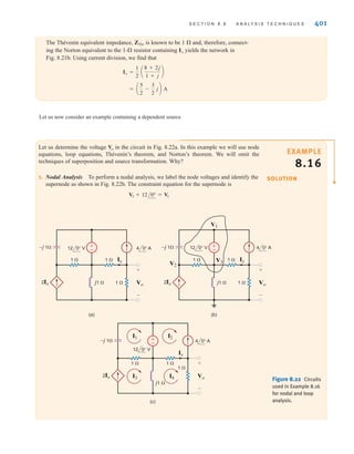
![402 C H A P T E R 8 A C S T E A D Y- S T A T E A N A LY S I S
and the KCL equations for the nodes of the network are
At this point we can solve the foregoing equations using a matrix analysis or, for exam-
ple, substitute the first and last equations into the remaining two equations, which yields
Solving these equations for yields
2. Loop Analysis The mesh currents for the network are defined in Fig. 8.22c. The
constraint equations for the circuit are
The KVL equations for mesh 1 and mesh 4 are
Note that if the constraint equations are substituted into the second KVL equation, the
only unknown in the equation is This substitution yields
and hence,
3. Thévenin’s Theorem In applying Thévenin’s theorem, we will find the open-circuit
voltage and then determine the Thévenin equivalent impedance using a test source at the
open-circuit terminals. We could determine the Thévenin equivalent impedance by calcu-
lating the short-circuit current; however, we will determine this current when we apply
Norton’s theorem.
The open-circuit voltage is determined from the network in Fig. 8.23a. Note that
and since flows through the inductor, the open-circuit voltage is
To determine the Thévenin equivalent impedance, we turn off the independent sources,
apply a test voltage source to the output terminals, and compute the current leaving the
test source. As shown in Fig. 8.23b, since flows in the test source, KCL requires
Ifl
x
= -4 + j8 V
Voc = -1A4/0°B + j1A2Iœ
xB
Voc
2Iœ
x
Iœ
x = 4/0° A
Vo = +4/143.13° V
I4 = +4/143.13° A
I4.
j1AI4 - I3B + 1AI4 - I2B + 1I4 = 0
-j1I1 + 1AI1 - I3B = -12/0°
I3 = 2Ix = 2I4 + 8/0°
Ix = I4 - I2 = I4 + 4/0°
I2 = -4/0°
= +4/143.13° V
Vo =
-(8 + j4)
1 + j2
Vo
-(4 + j2)Vo + (1 + j)V2 = 12 + j16
3Vo - (1 + j)V2 = -(4 + j12)
4/0° +
Vo - V3
1
+
Vo
1
= 0
V2 - V1
-j1
+
V2 - V3
1
- 2 a
V3 - Vo
1
b = 0
V1 - V2
-j1
+
V3 - V2
1
- 4/0° +
V3 - Vo
1
+
V3
j1
= 0
How does the presence of a
dependent source affect
superposition and source
exchange?
[ h i n t ]
irwin08_369-434hr.qxd 28-07-2010 12:03 Page 402](https://image.slidesharecdn.com/basic-engineering-circuit-analysis-10th-irwin-220801002926-2b111212/85/basic-engineering-circuit-analysis-10th-Irwin-pdf-426-320.jpg)
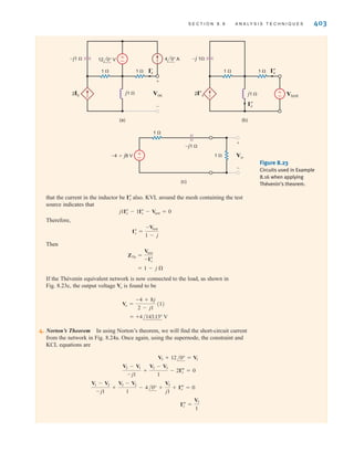
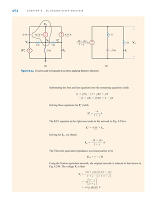
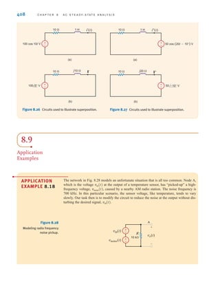
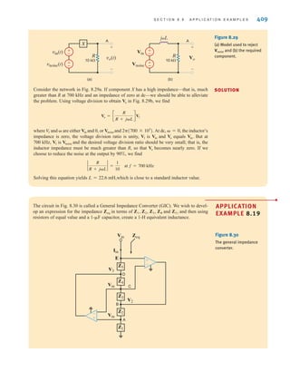
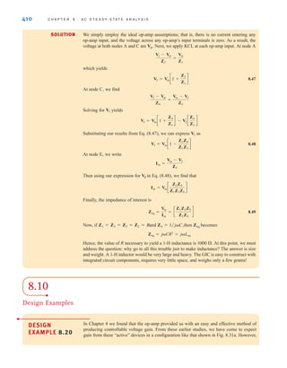
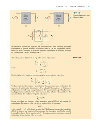
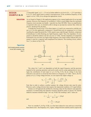
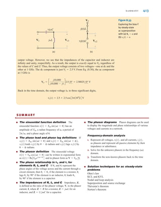
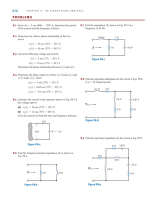
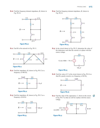
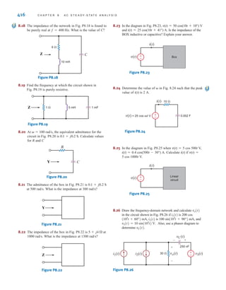
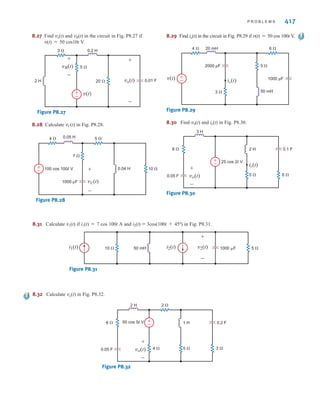
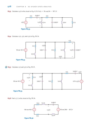
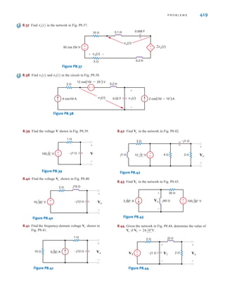
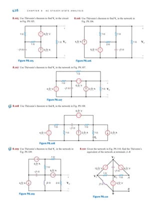
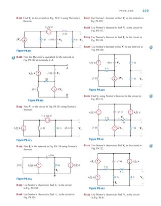
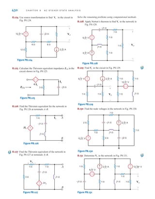
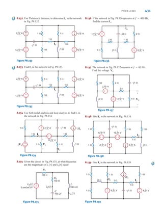
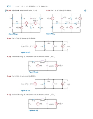
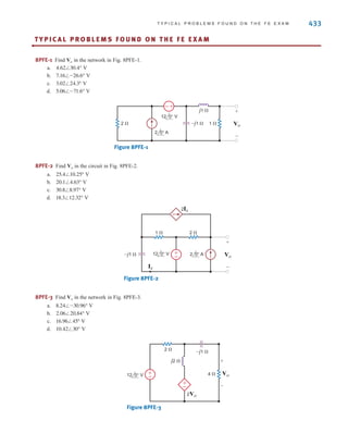
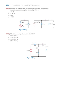

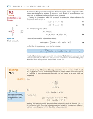
![EXAMPLE
9.1
SOLUTION
9.1
Instantaneous
Power
By employing the sign convention adopted in the earlier chapters, we can compute the instan-
taneous power supplied or absorbed by any device as the product of the instantaneous volt-
age across the device and the instantaneous current through it.
Consider the circuit shown in Fig. 9.1. In general, the steady-state voltage and current for
the network can be written as
9.1
9.2
The instantaneous power is then
9.3
Employing the following trigonometric identity,
9.4
we find that the instantaneous power can be written as
9.5
Note that the instantaneous power consists of two terms. The first term is a constant (i.e., it
is time independent), and the second term is a cosine wave of twice the excitation frequency.
We will examine this equation in more detail in Section 9.2.
p(t) =
V
MIM
2
CcosAv - iB + cosA2t + v + iBD
cos1 cos2 =
1
2
CcosA1 - 2B + cosA1 + 2BD
= V
MIM cosAt + vB cosAt + iB
p(t) = v(t)i(t)
i(t) = IM cosAt + iB
v(t) = V
M cosAt + vB
436 C H A P T E R 9 S T E A D Y- S T A T E P O W E R A N A LY S I S
±
– Z
v(t)
i(t)
Figure 9.1
Simple ac network.
The circuit in Fig. 9.1 has the following parameters: and
We wish to determine equations for the current and the instantaneous power
as a function of time and plot these functions with the voltage on a single graph for
comparison.
Since
then
From Eq. (9.5),
A plot of this function, together with plots of the voltage and current, is shown in Fig. 9.2.
As can be seen in this figure, the instantaneous power has a dc or constant term and a sec-
ond term whose frequency is twice that of the voltage or current.
= 3.46 + 4 cos(2t + 90°) W
p(t) = 4[cos(30°) + cos(2t + 90°)]
i(t) = 2 cos(t + 30°) A
= 2/30° A
I =
4/60°
2/30°
Z = 2/30° ⍀.
v(t) = 4 cos(t + 60°) V
Note that p(t) contains a dc
term and a cosine wave with
twice the frequency of v(t)
and i(t).
[ h i n t ]
irwin09_435-490hr.qxd 28-07-2010 12:00 Page 436](https://image.slidesharecdn.com/basic-engineering-circuit-analysis-10th-irwin-220801002926-2b111212/85/basic-engineering-circuit-analysis-10th-Irwin-pdf-461-320.jpg)
![S E C T I O N 9 . 2 A V E R A G E P O W E R 437
8.0
6.0
4.0
2.0
0.0
–2.0
–4.0
–6.0
–8.0
p(t)
i(t)
v(t)
0.000 0.003 0.006 0.009 0.012 0.015 0.018 0.021 0.024 0.027 0.030
t(s)
Figure 9.2
Plots of v(t), i(t), and p(t) for
the circuit in Example 9.1
using f ⫽ 60 Hz.
The average value of any periodic waveform (e.g., a sinusoidal function) can be computed by
integrating the function over a complete period and dividing this result by the period. Therefore,
if the voltage and current are given by Eqs. (9.1) and (9.2), respectively, the average power is
9.6
where is arbitrary, is the period of the voltage or current, and P is measured in
watts. Actually, we may average the waveform over any integral number of periods so that
Eq. (9.6) can also be written as
9.7
where n is a positive integer.
Employing Eq. (9.5) for the expression in (9.6), we obtain
9.8
We could, of course, plod through the indicated integration; however, with a little forethought
we can determine the result by inspection. The first term is independent of t, and therefore a con-
stant in the integration. Integrating the constant over the period and dividing by the period simply
results in the original constant. The second term is a cosine wave. It is well known that the aver-
age value of a cosine wave over one complete period or an integral number of periods is zero, and
therefore the second term in Eq. (9.8) vanishes. In view of this discussion, Eq. (9.8) reduces to
9.9
Note that since the argument for the cosine function can be either
or In addition, note that is the angle of the circuit impedance as
shown in Fig. 9.1. Therefore, for a purely resistive circuit,
9.10
P =
1
2
V
MIM
v - i
i - v.
v - i
cos(-) = cos(),
P =
1
2
V
MIM cosAv - iB
P =
1
T 3
t0 +T
t0
V
MIM
2
Ccos(v - i) + cos(2t + v + i)D dt
P =
1
nT 3
t0 +nT
t0
V
MIM cos(t + v) cos(t + i) dt
T = 2兾
t0
=
1
T 3
t0 +T
t0
V
MIM cosAt + vB cosAt + iB dt
P =
1
T 3
t0 +T
t0
p(t) dt
9.2
Average Power
A frequently used equation
for calculating the average
power.
[ h i n t ]
irwin09_435-490hr.qxd 28-07-2010 12:00 Page 437](https://image.slidesharecdn.com/basic-engineering-circuit-analysis-10th-irwin-220801002926-2b111212/85/basic-engineering-circuit-analysis-10th-Irwin-pdf-462-320.jpg)
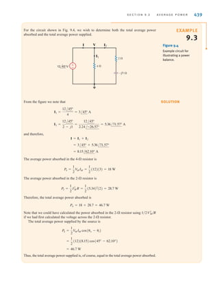
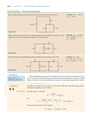
![440 C H A P T E R 9 S T E A D Y- S T A T E P O W E R A N A LY S I S
When determining average power, if more than one source is present in a network, we can use
any of our network analysis techniques to find the necessary voltage and/or current to compute
the power. However, we must remember that in general we cannot apply superposition to power.
E9.1 Find the average power absorbed by each resistor in the network in Fig. E9.1.
Learning Assessments
ANSWER:
P4⍀ = 7.20 W.
P2⍀ = 7.20 W;
E9.2 Given the network in Fig. E9.2, find the average power absorbed by each passive circuit
element and the total average power supplied by the current source.
ANSWER:
PCS = 90.50 W.
PL = 0;
P4⍀ = 33.96 W;
P3⍀ = 56.60 W;
±
–
2 ⍀
4 ⍀ –j4 ⍀
12 60° V
Figure E9.1
3 ⍀
4 ⍀
j2 ⍀
10 30° A
Figure E9.2
Superposition is not
applicable to power. Why?
[ h i n t ]
E9.3 Find the power supplied and the power absorbed by each element in Fig. E9.3.
–j2 ⍀ –j2 ⍀
2 ⍀
4 ⍀
j2 ⍀
2 0° A
Figure E9.3
EXAMPLE
9.4
SOLUTION
Consider the network shown in Fig. 9.5. We wish to determine the total average power
absorbed and supplied by each element.
From the figure we note that
and
The power absorbed by the 2-⍀ resistor is
P2 =
1
2
V
MIM =
1
2
(12)(6) = 36 W
I3 =
12/30° - 6/0°
j1
=
4.39 + j6
j1
= 7.44/-36.21° A
I2 =
12/30°
2
= 6/30° A
ANSWER: PC = 0 W;
PL = 0 W; P4⍀ = 1.78 W;
P2⍀ = 2.22 W; PCS = -4 W.
irwin09_435-490hr.qxd 28-07-2010 12:00 Page 440](https://image.slidesharecdn.com/basic-engineering-circuit-analysis-10th-irwin-220801002926-2b111212/85/basic-engineering-circuit-analysis-10th-Irwin-pdf-465-320.jpg)
![S E C T I O N 9 . 2 A V E R A G E P O W E R 441
±
–
±
–
2 ⍀
j1 ⍀
I1 I3
I2
12 30° V 6 0° V
Figure 9.5
Example RL circuit with
two sources.
Under the following condition:
if P ⫽ IV is positive, power is
being absorbed.
If P ⫽ IV is negative, power is
being generated.
±
–
I
V
[ h i n t ]
According to the direction of I3, the source is absorbing power. The power it
absorbs is given by
At this point an obvious question arises: how do we know whether the source is
supplying power to the remainder of the network or absorbing it? The answer to this question
is actually straightforward. If we employ our passive sign convention that was adopted in the
earlier chapters—that is, if the current reference direction enters the positive terminal of
the source and the answer is positive—the source is absorbing power. If the answer is negative,
the source is supplying power to the remainder of the circuit. A generator sign convention could
have been used, and under this condition the interpretation of the sign of the answer would be
reversed. Note that once the sign convention is adopted and used, the sign for average power
will be negative only if the angle difference is greater than 90°
To obtain the power supplied to the network, we compute I1 as
Therefore, the power supplied by the source using the generator sign convention is
and hence the power absorbed is equal to the power supplied.
= 54 W
PS =
1
2
(12)(11.29) cos(30° + 7.10°)
12/30°-V
= 11.29/-7.10° A
= 6/30° + 7.44/-36.21°
I1 = I2 + I3
Ai.e., @v - i @ 7 90°B.
6/0°-V
= 18 W
=
1
2
(6)(7.44) cos[0° - (-36.21°)]
P6/0° =
1
2
V
MIM cos(v - i)
6/0°-V
E9.4 Determine the total average power absorbed and supplied by each element in the network
in Fig. E9.4.
Learning Assessments
ANSWER:
PC = 0.
P4⍀ = 49.6 W;
PVS = 19.8 W;
PCS = -69.4 W;
±
–
12 0° A 4 30° V
–j2 ⍀
4 ⍀
Figure E9.4
irwin09_435-490hr.qxd 28-07-2010 12:00 Page 441](https://image.slidesharecdn.com/basic-engineering-circuit-analysis-10th-irwin-220801002926-2b111212/85/basic-engineering-circuit-analysis-10th-Irwin-pdf-466-320.jpg)
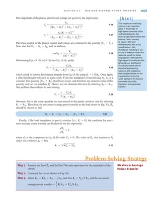
![S E C T I O N 9 . 3 M A X I M U M A V E R A G E P O W E R T R A N S F E R 443
The magnitude of the phasor current and voltage are given by the expressions
9.16
9.17
The phase angles for the phasor current and voltage are contained in the quantity
Note also that and, in addition,
9.18
Substituting Eqs. (9.16) to (9.18) into Eq. (9.11) yields
9.19
which could, of course, be obtained directly from Eq. (9.16) using Once again,
a little forethought will save us some work. From the standpoint of maximizing is a
constant. The quantity absorbs no power, and therefore any nonzero value of this
quantity only serves to reduce Hence, we can eliminate this term by selecting XL = -XTh.
Our problem then reduces to maximizing
9.20
However, this is the same quantity we maximized in the purely resistive case by selecting
Therefore, for maximum average power transfer to the load shown in Fig. 9.6, ZL
should be chosen so that
9.21
Finally, if the load impedance is purely resistive the condition for maxi-
mum average power transfer can be derived via the expression
where is the expression in Eq. (9.19) with XL=0. The value of that maximizes
under the condition XL=0 is
9.22
RL = 2R2
Th + X2
Th
PL
RL
PL
dPL
dRL
= 0
Ai.e., XL = 0B,
ZL = RL + jXL = RTh - jXTh = Z*
Th
RL = RTh.
PL =
1
2
V2
ocRL
ARL + RThB
2
PL.
AXTh + XLB
V
oc
PL,
PL = 1
2 I2
LRL.
PL =
1
2
V2
ocRL
ARTh + RLB
2
+ AXTh + XLB
2
cosZL
=
RL
AR2
L + X2
LB
1兾2
vL
- iL
= ZL
AvL
- iL
B.
V
L =
V
ocAR2
L + X2
LB
1兾2
CARTh + RLB
2
+ AXTh + XLB
2
D1兾2
IL =
Voc
CARTh + RLB
2
+ AXTh + XLB
2
D1兾2
This impedance-matching
concept is an important
issue in the design of
high-speed computer chips
and motherboards. For
today’s high-speed chips with
internal clocks running
at about 3 GHz and
motherboards with a bus
speed above 1 GHz,
impedance matching is nec-
essary in order to obtain the
required speed for signal
propagation. Although this
high-speed transmission line
is based on a distributed
circuit (discussed later in
electrical engineering
courses), the impedance-
matching technique for the
transmission line is the
same as that of the lumped
parameter circuit for
maximum average power
transfer.
[ h i n t ]
Step 1. Remove the load ZL and find the Thévenin equivalent for the remainder of the
circuit.
Step 2. Construct the circuit shown in Fig. 9.6.
Step 3. Select and then and the maximum
average power transfer =
1
2
I2
LRTh = V2
oc兾8 RTh.
IL = Voc兾2 RTh
ZL = Z*
Th = RTh - jXTh,
Problem-Solving Strategy
Maximum Average
Power Transfer
irwin09_435-490hr.qxd 28-07-2010 12:00 Page 443](https://image.slidesharecdn.com/basic-engineering-circuit-analysis-10th-irwin-220801002926-2b111212/85/basic-engineering-circuit-analysis-10th-Irwin-pdf-468-320.jpg)
![444 C H A P T E R 9 S T E A D Y- S T A T E P O W E R A N A LY S I S
In this Thévenin analysis,
1. Remove ZL and find the
voltage across the open
terminals, Voc .
2. Determine the impedance
ZTh at the open terminals
with all independent
sources made zero.
3. Construct the following
circuit and determine I and
PL.
[ h i n t ]
±
–
ZTh
I
Voc ZTh
*
(a) (b)
(c)
ZL
j1 ⍀
2 ⍀ 4 ⍀
4 0° A
j1 ⍀
2 ⍀ 4 ⍀
4 0° A
ZTh
j1 ⍀
2 ⍀ 4 ⍀
Voc
+
-
Figure 9.7
Circuits for illustrating
maximum average
power transfer.
EXAMPLE
9.5
SOLUTION
Given the circuit in Fig. 9.7a, we wish to find the value of ZL for maximum average power
transfer. In addition, we wish to find the value of the maximum average power delivered to
the load.
To solve the problem, we form a Thévenin equivalent at the load. The circuit in Fig. 9.7b is
used to compute the open-circuit voltage
The Thévenin equivalent impedance can be derived from the circuit in Fig. 9.7c. As shown
in the figure,
Therefore, ZL for maximum average power transfer is
With ZL as given previously, the current in the load is
Therefore, the maximum average power transferred to the load is
PL =
1
2
I2
MRL =
1
2
(1.87)2
(1.41) = 2.47 W
I =
5.26/-9.46°
2.82
= 1.87/-9.46° A
ZL = 1.41 - j0.43 ⍀
ZTh =
4(2 + j1)
6 + j1
= 1.41 + j0.43 ⍀
Voc =
4/0° (2)
6 + j1
(4) = 5.26/-9.46° V
EXAMPLE
9.6
SOLUTION
For the circuit shown in Fig. 9.8a, we wish to find the value of ZL for maximum average
power transfer. In addition, let us determine the value of the maximum average power deliv-
ered to the load.
We will first reduce the circuit, with the exception of the load, to a Thévenin equivalent circuit.
The open-circuit voltage can be computed from Fig. 9.8b. The equations for the circuit are
Vœ
x = -2I1
Vœ
x + 4 = (2 + j4)I1
irwin09_435-490hr.qxd 28-07-2010 12:00 Page 444](https://image.slidesharecdn.com/basic-engineering-circuit-analysis-10th-irwin-220801002926-2b111212/85/basic-engineering-circuit-analysis-10th-Irwin-pdf-469-320.jpg)
![S E C T I O N 9 . 3 M A X I M U M A V E R A G E P O W E R T R A N S F E R 445
When there is a dependent
source, both Voc and Isc must
be found and ZTh computed
from the equation
ZTh =
Voc
Isc
[ h i n t ]
Solving for I1, we obtain
The open-circuit voltage is then
The short-circuit current can be derived from Fig. 9.8c. The equations for this circuit are
Solving these equations for Isc yields
The Thévenin equivalent impedance is then
Therefore, for maximum average power transfer the load impedance should be
The current in this load ZL is then
Hence, the maximum average power transferred to the load is
= 1.25 W
PL =
1
2
(1.58)2
(1)
IL =
Voc
ZTh + ZL
=
-3 - j1
2
= 1.58/-161.57° A
ZL = 1 + j1 ⍀
ZTh =
Voc
Isc
=
3 + j1
1 + j2
= 1 - j1 ⍀
Isc = -(1 + j2) A
Vfl
x = -2AI - IscB
-4 = -2I + (2 - j2)Isc
Vfl
x + 4 = (2 + j4)I - 2Isc
= +3.16/-161.57° V
= -3 - j1
= 22/-45° - 4/0°
Voc = 2I1 - 4/0°
I1 =
1/-45°
12
(a)
4 0° V
j4 ⍀
2 ⍀
–j2 ⍀
±
– ZL
±
–
Vx
Vx
-
+
(b)
4 0° V
j4 ⍀
2 ⍀
–j2 ⍀
±
–
±
–
I1
V'
x Voc
+
-
V'
x
(c)
4 0° V
j4 ⍀ –j2 ⍀
±
–
±
–
Isc
I
V
x
2 ⍀
V
x
-
+
-
+
Figure 9.8
Circuits for illustrating maximum average power transfer.
irwin09_435-490hr.qxd 28-07-2010 12:00 Page 445](https://image.slidesharecdn.com/basic-engineering-circuit-analysis-10th-irwin-220801002926-2b111212/85/basic-engineering-circuit-analysis-10th-Irwin-pdf-470-320.jpg)
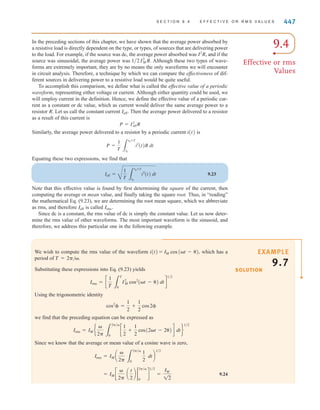
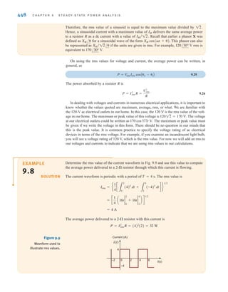
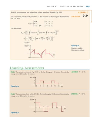
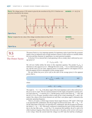
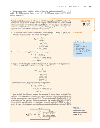
![S E C T I O N 9 . 5 T H E P O W E R F A C T O R 451
EXAMPLE
9.10
SOLUTION
In a similar manner, an RL load has a lagging pf; therefore, load impedances of ZL = 1 - j1 ⍀
and ZL = 2 + j1 ⍀ have power factors of cos(-45°) = 0.707 leading and cos(26.57°) = 0.894
lagging, respectively.
An industrial load consumes 88 kW at a pf of 0.707 lagging from a 480-V rms line. The
transmission line resistance from the power company’s transformer to the plant is 0.08 ⍀.
Let us determine the power that must be supplied by the power company (a) under present
conditions and (b) if the pf is somehow changed to 0.90 lagging. (It is economically advan-
tageous to have a power factor as close to one as possible.)
a. The equivalent circuit for these conditions is shown in Fig. 9.11. Using Eq. (9.27), we
obtain the magnitude of the rms current into the plant:
The power that must be supplied by the power company is
b. Suppose now that the pf is somehow changed to 0.90 lagging but the voltage remains
constant at 480 V. The rms load current for this condition is
Under these conditions, the power company must generate
Note carefully the difference between the two cases. A simple change in the pf of the
load from 0.707 lagging to 0.90 lagging has had an interesting effect. Note that in the first
case the power company must generate 93.38 kW in order to supply the plant with 88 kW
of power because the low power factor means that the line losses will be high—5.38 kW.
However, in the second case the power company need only generate 91.32 kW in order to
supply the plant with its required power, and the corresponding line losses are only 3.32 kW.
= 91.32 kW
= 88,000 + (0.08)(203.7)2
PS = PL + (0.08)I2
rms
= 203.7 A rms
=
(88)A103
B
(0.90)(480)
Irms =
PL
(pf)AVrmsB
= 93.38 kW
= 88,000 + (0.08)(259.3)2
PS = PL + (0.08)I2
rms
= 259.3 A rms
=
(88)A103
B
(0.707)(480)
Irms =
PL
(pf)AVrmsB
±
–
PL=88 kW
pf=0.707 lagging
Irms
VS 480 V rms
0.08 ⍀ Figure 9.11
Example circuit for
examining changes in
power factor.
Technique
1. Given PL, pf, and Vrms,
determine Irms.
2. Then Rline,
where Rline is the line
resistance.
PS = PL + I2
rms
[ h i n t ]
irwin09_435-490hr.qxd 28-07-2010 12:00 Page 451](https://image.slidesharecdn.com/basic-engineering-circuit-analysis-10th-irwin-220801002926-2b111212/85/basic-engineering-circuit-analysis-10th-Irwin-pdf-476-320.jpg)
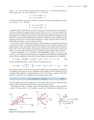
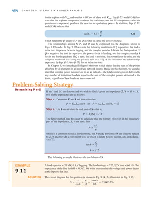
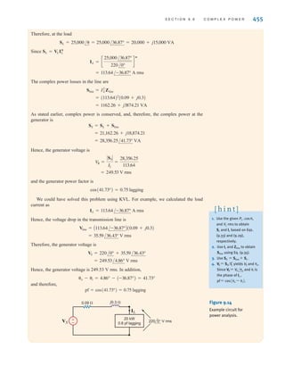
![S E C T I O N 9 . 6 C O M P L E X P O W E R 455
Therefore, at the load
Since
The complex power losses in the line are
As stated earlier, complex power is conserved, and, therefore, the complex power at the
generator is
Hence, the generator voltage is
and the generator power factor is
We could have solved this problem using KVL. For example, we calculated the load
current as
Hence, the voltage drop in the transmission line is
Therefore, the generator voltage is
Hence, the generator voltage is 249.53 V rms. In addition,
and therefore,
pf = cos(41.73°) = 0.75 lagging
v - i = 4.86° - (-36.87°) = 41.73°
= 249.53/4.86° V rms
VS = 220/0° + 35.59/36.43°
= 35.59/36.43° V rms
Vline = A113.64/-36.87°B(0.09 + j0.3)
IL = 113.64/-36.87° A rms
cos(41.73°) = 0.75 lagging
= 249.53 V rms
V
S =
@SS @
IL
=
28,356.25
113.64
= 28,356.25/41.73° VA
= 21,162.26 + j18,874.21
SS = SL + Sline
= 1162.26 + j3874.21 VA
= (113.64)2
(0.09 + j0.3)
Sline = I2
LZline
= 113.64/-36.87° A rms
IL = c
25,000/36.87°
220/0°
d
*
SL = VLI*
L
SL = 25,000/ = 25,000/36.87° = 20,000 + j15,000 VA
±
–
20 kW
0.8 pf lagging
IL
VS
0.09 ⍀ j0.3 ⍀
220 0° V rms
Figure 9.14
Example circuit for
power analysis.
1. Use the given ,
and rms to obtain
SL and IL based on Eqs.
(9.33) and (9.29),
respectively.
2. Use IL and Zline to obtain
Sline using Eq. (9.35).
3. Use SS = Sline + SL.
4. VS = SS yields VS and v.
Since VS = VS and i is
the phase of IL ,
pf = cos Av - iB.
/v
兾I*
L
VL
PL, cos
[ h i n t ]
irwin09_435-490hr.qxd 28-07-2010 12:00 Page 455](https://image.slidesharecdn.com/basic-engineering-circuit-analysis-10th-irwin-220801002926-2b111212/85/basic-engineering-circuit-analysis-10th-Irwin-pdf-480-320.jpg)
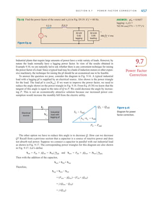
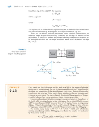
![Recall from Eqs. (9.36) and (9.37) that in general
S = V2
rms/Z*
and for a capacitor
Z* = -1/jC
so that
Scap = Qcap = -jCV2
rms
This equation can be used to find the required value of C in order to achieve the new speci-
fied power factor defined by the new power factor angle illustrated in Fig. 9.17.
Hence, we can obtain a particular power factor for the total load (industrial load and
capacitor) simply by judiciously selecting a capacitor and placing it in parallel with the
original load. In general, we want the power factor to be large, and therefore the power fac-
tor angle must be small [i.e., the larger the desired power factor, the smaller the angle
].
AvL
- iT
B
458 C H A P T E R 9 S T E A D Y- S T A T E P O W E R A N A LY S I S
Electrical
source
Industrial
load with
lagging pf
VL
IT IL
C
+
-
vL
– iL
=old
PL=Pold
SL=Sold
QL=Qold
Qcap
new
vL
– iT
=new
PL=Pold
Snew
Qnew
Figure 9.17
Power factor correction
diagram including capacitor.
EXAMPLE
9.13
Every month our electrical energy provider sends us a bill for the amount of electrical
energy that we have consumed. The rate is often expressed in cents per kWh and consists
of at least two components: (1) the demand charge, which covers the cost of lines, poles,
transformers, and so on, and (2) the energy charge, which covers the cost to produce elec-
tric energy at power plants. The energy charge is the subject of the deregulation of the elec-
tric utility industry where you, as a customer, choose your energy provider.
It is common for an industrial facility operating at a poor power factor to be charged more by
the electric utility providing electrical service. Let’s suppose that our industrial facility operates
at and requires 500 kW at a power factor of 0.75 lagging. Assume an energy charge
of 2¢ per kWh and a demand charge of $3.50 per kW per month if the power factor is between
0.9 lagging and unity and $5 per kVA per month if the power factor is less than 0.9 lagging.
The monthly energy charge is Let’s calculate the
monthly demand charge with the 0.75 lagging power factor. The complex power absorbed
by the industrial facility is
Sold =
500
0.75
/cos-1
(0.75) = 666.67/41.4° = 500 + j441 kVA
500 * 24 * 30 * $0.02 = $7200.
277 V rms
irwin09_435-490hr.qxd 28-07-2010 12:00 Page 458](https://image.slidesharecdn.com/basic-engineering-circuit-analysis-10th-irwin-220801002926-2b111212/85/basic-engineering-circuit-analysis-10th-Irwin-pdf-483-320.jpg)
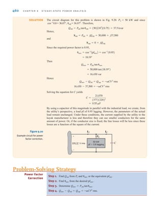
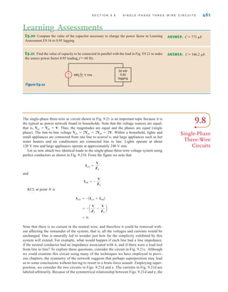
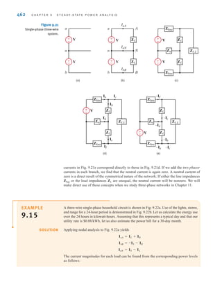
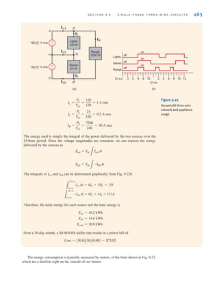

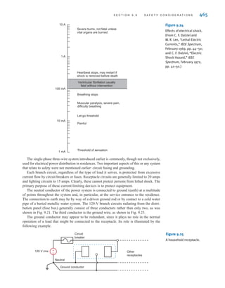
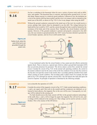
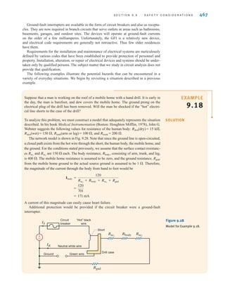
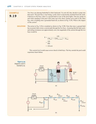
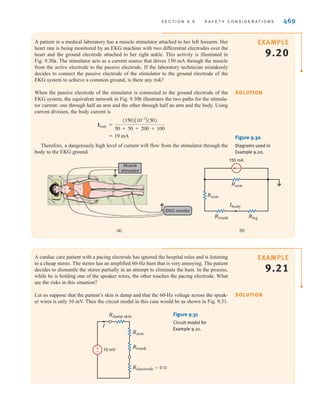
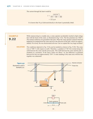

![S E C T I O N 9 . 9 S A F E T Y C O N S I D E R A T I O N S 471
The examples of this section have been provided in an attempt to illustrate some of the
potential dangers that exist when working or playing around electric power. In the worst case,
failure to prevent an electrical accident can result in death. However, even nonlethal electrical
contacts can cause such things as burns or falls. Therefore, we must always be alert to ensure
not only our own safety, but also that of others who work and play with us.
The following guidelines will help minimize the chances of injury:
1. Avoid working on energized electrical systems.
2. Always assume that an electrical system is energized unless you can absolutely verify
that it is not.
3. Never make repairs or alterations that are not in compliance with the provisions of the
prevailing code.
4. Do not work on potentially hazardous electrical systems alone.
5. If another person is “frozen” to an energized electrical circuit, deenergize the circuit, if
possible. If that cannot be done, use nonconductive material such as dry wooden
boards, sticks, belts, and articles of clothing to separate the body from the contact. Act
quickly but take care to protect yourself.
6. When handling long metallic equipment, such as ladders, antennas, and so on,
outdoors, be continuously aware of overhead power lines and avoid any possibility of
contact with them.
Safety guidelines.
[ h i n t ]
E9.22 A woman is driving her car in a violent rainstorm. While she is waiting at an intersec-
tion, a power line falls on her car and makes contact. The power line voltage is 7200 V.
(a) Assuming that the resistance of the car is negligible, what is the potential current
through her body if, while holding the door handle with a dry hand, she steps out
onto the wet ground?
(b) If she remained in the car, what would happen?
Learning Assessment
ANSWER: (a) I = 463 mA,
extremely dangerous;
(b) she should be safe.
Safety when working with electric power must always be a primary consideration.
Regardless of how efficient or expedient an electrical network is for a particular application,
it is worthless if it is also hazardous to human life.
The safety device shown in Fig. 9.33, which is also used for troubleshooting, is a
proximity-type sensor that will indicate whether a circuit is energized by simply touching the
conductor on the outside of the insulation. This device is typically carried by all electricians
and is helpful when working on electric circuits.
In addition to the numerous deaths that occur each year due to electrical accidents, fire
damage that results from improper use of electrical wiring and distribution equipment
amounts to millions of dollars per year.
To prevent loss of life and damage to property, very detailed procedures and specifications
have been established for the construction and operation of electrical systems to ensure their
safe operation. The National Electrical Code ANSI C1 (ANSI—American National
Figure 9.33
A modern safety or
troubleshooting device.
(Courtesy of Fluke
Corporation. Reproduced
with permission.)
irwin09_435-490hr.qxd 28-07-2010 12:00 Page 471](https://image.slidesharecdn.com/basic-engineering-circuit-analysis-10th-irwin-220801002926-2b111212/85/basic-engineering-circuit-analysis-10th-Irwin-pdf-496-320.jpg)
![S E C T I O N 9 . 1 0 A P P L I C A T I O N E X A M P L E S 473
SOLUTION
APPLICATION
EXAMPLE 9.25
If cord is the length of the extension cord, then for 16-gauge wire we find
and for 14-gauge wire
/cord =
Rcord
0.0025
= 152.8 feet
/cord =
Rcord
0.004
= 95.5 feet
/
120 V rms 110 V rms
Mower
13.1 A rms
Rcord
Vcord=5 V rms
Vcord=5 V rms
Rcord
±
–
± –
±
–
±
–
Figure 9.35
Circuit model in
Example 9.24.
While sitting in a house reading a book, we notice that every time the air conditioner
comes on, the lights momentarily dim. Let us investigate this phenomenon using the
single-phase three-wire circuit shown in Fig. 9.36a and some typical current requirements
for a 10,000-Btu/h air conditioner, assuming a line resistance of 0.5 ⍀.
The 60-W light bulb can be roughly modeled by its equivalent resistance:
or
When the air conditioner unit first turns on, the current requirement is 40 A, as shown in
Fig. 9.36b. As the compressor motor comes up to speed, the current requirement drops
quickly to a steady-state value of 10 A, as shown in Fig. 9.36c. We will compare the volt-
age across the light fixture, both at turn-on and in steady state.
Using superposition, let us first find that portion of caused by the voltage sources.
The appropriate circuit is shown in Fig. 9.36d. Using voltage division, we find that
or
Figure 9.36e will yield the contribution to caused by the 10-A steady-state current.
Using current division to calculate the current through the light bulb, we find that
or
Therefore, the steady-state value of is
At start-up, our expression for can be used with which yields
The resulting value for is
The voltage delivered to the light fixture at startup is 13% lower than the steady-state value,
resulting in a momentary dimming of the lights.
VAN = V
AN1 + V
AN2 = 119.50 - 19.92 = 99.58 V rms
V
AN
V
AN2 = -19.92 V rms.
IAB = 40 A,
VAN2
V
AN = V
AN1 + V
AN2 = 114.52 V rms
V
AN
V
AN2 = -4.98 V rms
V
AN2 = - eIAB a
RL
Rbulb + 2RL
b fRbulb
V
AN
V
AN1 = 119.50 V rms
V
AN1 = V
AN a
Rbulb
Rbulb + 2RL
b
V
AN
V
AN,
Rbulb = 240 ⍀
Pbulb =
V2
an
Rbulb
Technique
1. Find the resistance of the
light bulb.
2. Use a large current source
to represent the transient
current of the air condi-
tioner and a small current
source to represent the
steady-state current.
3. Find the voltage drop
across the light bulb dur-
ing both the transient and
steady-state operations.
[ h i n t ]
irwin09_435-490hr.qxd 28-07-2010 12:00 Page 473](https://image.slidesharecdn.com/basic-engineering-circuit-analysis-10th-irwin-220801002926-2b111212/85/basic-engineering-circuit-analysis-10th-Irwin-pdf-498-320.jpg)
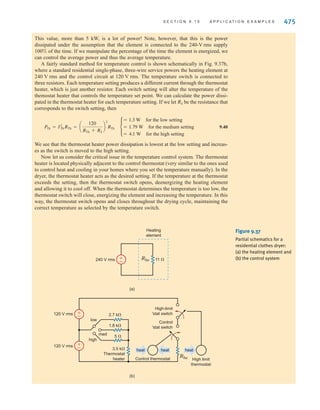
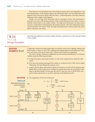
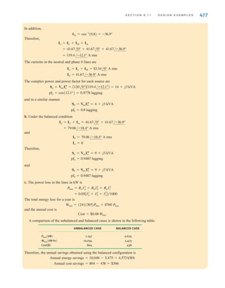
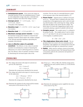
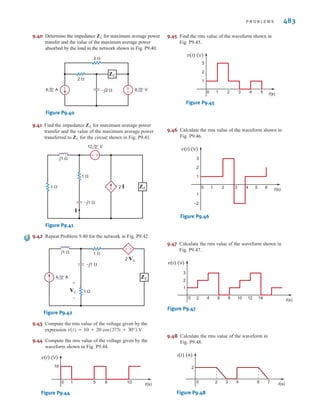
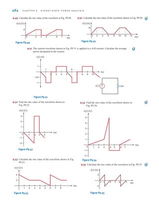
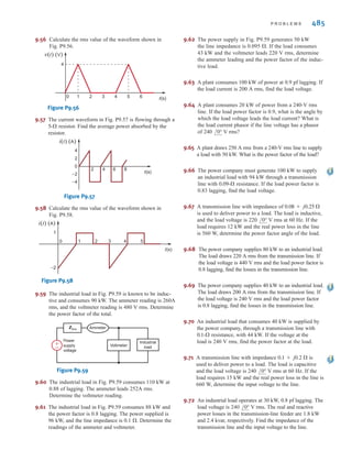
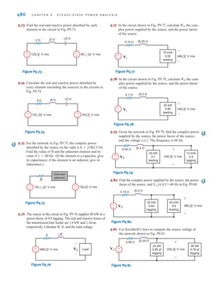
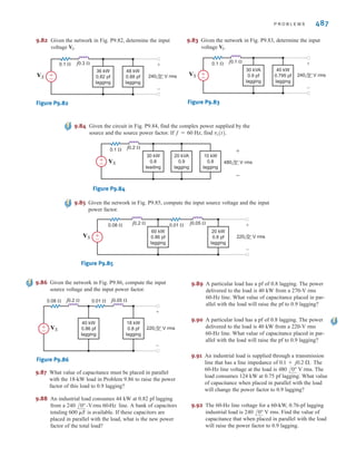
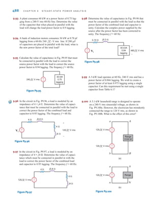
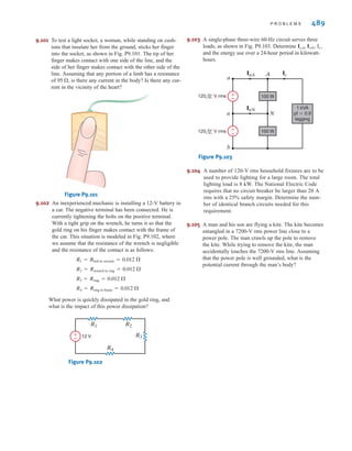
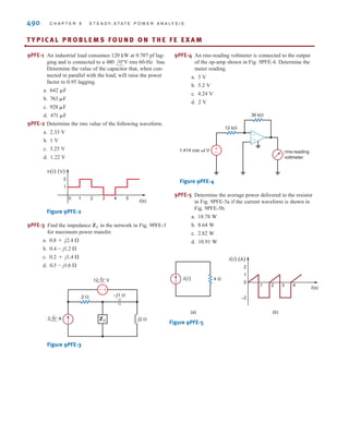

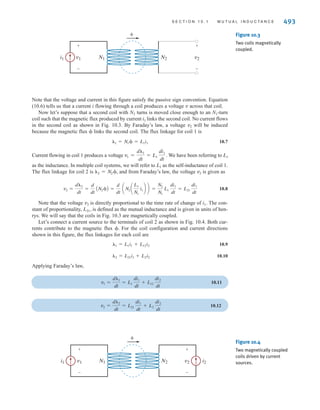
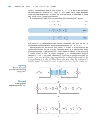
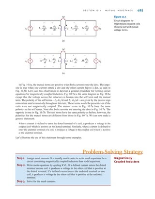
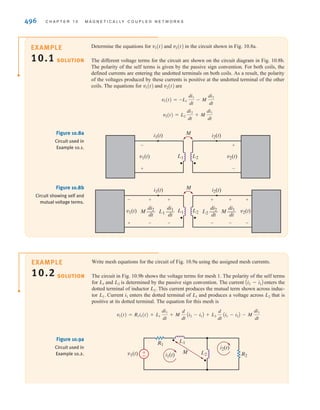
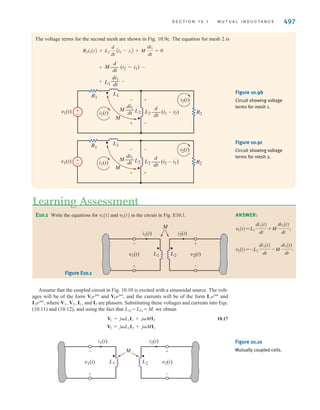
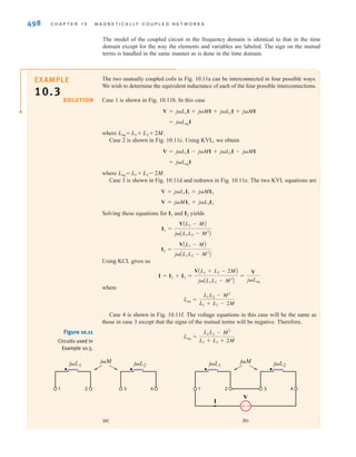
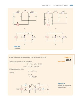
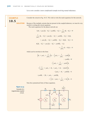
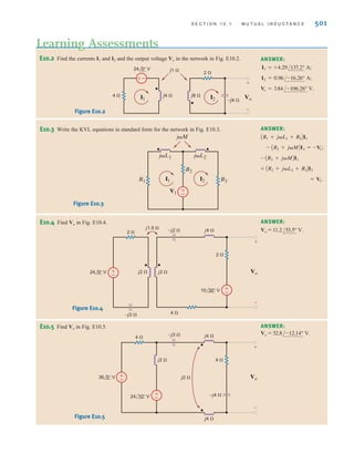
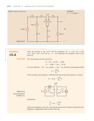
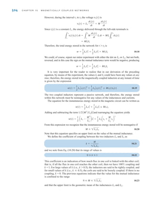
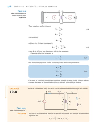
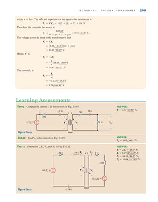
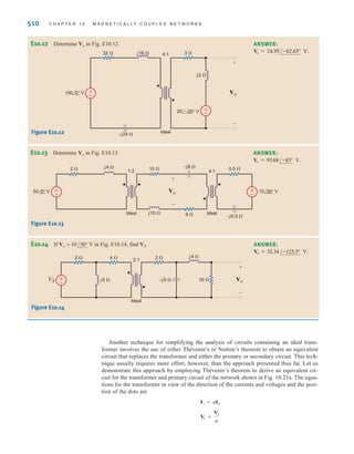
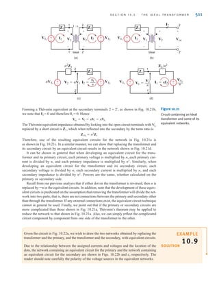
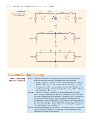
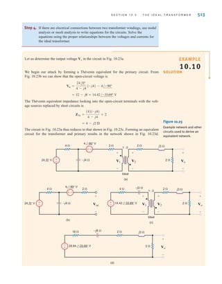
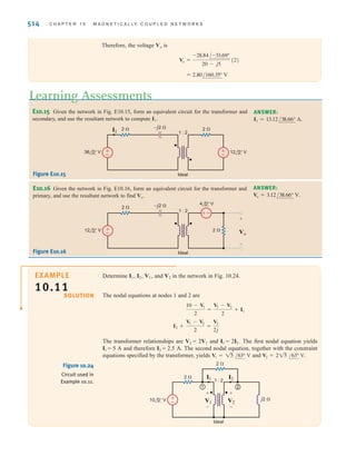
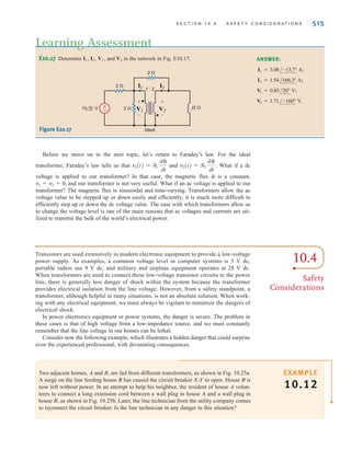
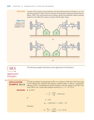
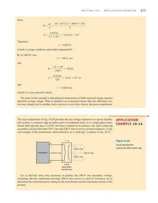
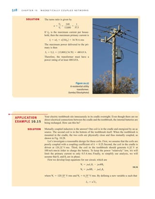
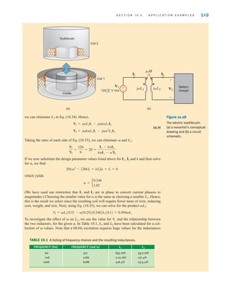
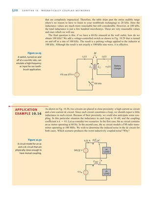
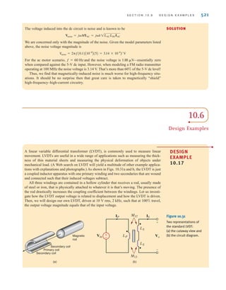
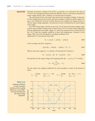
![522 C H A P T E R 1 0 M A G N E T I C A L LY C O U P L E D N E T W O R K S
Typically, the primary winding of the LVDT is excited by an ac sinusoid in the range of
3 to 30 V rms at frequencies between 400 and 5000 Hz. Since we only need to measure the
output voltage directly with a voltmeter, no external load is necessary.
The null position for the rod is dead center between the secondary windings. In that posi-
tion the coupling between the primary and each secondary is identical, and the output volt-
age is zero. Should the rod move in either direction, the coupling will change linearly, as
will the output voltage magnitude. The direction of travel is indicated by the relative phase
of the output.
Our LVDT design begins with the circuit in Fig. 10.31b where the mutual coupling coeffi-
cient for each secondary winding varies as shown in Fig. 10.32. To create a linear relationship
between displacement and output voltage, we restrict the nominal travel to that portion of
Fig. 10.32 where the coupling coefficient is linear with displacement. Therefore, in this
design, 100% travel will correspond to a coupling coefficient of 0.8.
Applying KVL to the primary loop yields
10.36
At the secondary, the KVL equation is
10.37
With no load at the output, and Eqs. (10.36) and (10.37) reduce to
10.38
Solving these for the output voltage and recognizing that we obtain
10.39
We can express the coupling coefficients for each secondary in terms of the percent of
travel:
k12 = b
0.008x
0
for 0 6 x 6 100
for x 6 0
k13 = b
0.008x
0
for -100 6 x 6 0
for x 7 0
Vo = Vin
B
LS
LP
Ck12 - k13 D
MlX = klX CLPLS D
0.5
,
Vin = jLPIP and Vo = IPjCM12 - M13 D
IS= 0
2AjLSBIS + jM13IP - jM12IP + Vo = 0
Vin = jLPIP + jM13IS - jM12IS
[k12-k13]
k13 k12
1.2
1
0.8
0.6
0.4
0.2
0
–0.2
–200 –150 –100 –50 0 50 100 150 200
Coupling
Coefficient
Travel
Figure 10.32
Coupling coefficients
for each secondary
winding and the coupling
difference. It is the differ-
ence that will determine
the output voltage
magnitude.
SOLUTION
irwin10_491-540hr.qxd 28-07-2010 12:10 Page 522](https://image.slidesharecdn.com/basic-engineering-circuit-analysis-10th-irwin-220801002926-2b111212/85/basic-engineering-circuit-analysis-10th-Irwin-pdf-547-320.jpg)
![S E C T I O N 1 0 . 6 D E S I G N E X A M P L E S 523
And, finally, assuming that the input voltage has zero phase angle, the output voltage can be
expressed as
10.40
Note the phase angle difference for positive versus negative travel.
To complete our analysis, we must determine a value for the secondary to primary induc-
tance ratio. At 100% travel, the magnitudes of the input and output voltages are equal and
Using this information in Eq. (10.40), we find that the inductor ratio must be
To determine actual values for the inductances, we must consider the input current we will
tolerate at the primary. We would prefer a relatively small current, because a large current would
require large-diameter wire in the primary winding. Let us choose a primary current of
25 mA rms with an excitation of 10 V rms at 2000 Hz. From Eq. (10.38), the primary inductance
will be
which yields a secondary inductance of
The selection of the two inductances completes this design.
LS = 1.5625LP = 49.7 mH
LP =
Vin
IP
=
10
2(2000)(0.025)
= 31.8 mH
LS兾LP = 1.252
= 1.5625.
k = 0.8.
Vo = Vin
B
LS
LP
[-0.008x] = Vin
B
LS
LP
[+0.008x]/-180° -100 6 x 6 0
Vo = Vin
B
LS
LP
[0.008x] = Vin
B
LS
LP
[0.008x]/0° 0 6 x 6 100
The next example illustrates a technique for employing a transformer in a configuration that
will extend the life of a set of Christmas tree lights.
DESIGN
EXAMPLE
10.18
The bulbs in a set of Christmas tree lights normally operate at 120 V rms. However, they last
much longer if they are instead connected to 108 V rms. Using a 120 V-12 V transformer,
let us design an autotransformer that will provide 108 V rms to the bulbs.
The two-winding transformers we have presented thus far provide electrical isolation
between primary and secondary windings, as shown in Fig. 10.33a. It is possible, howev-
er, to interconnect primary and secondary windings serially, creating a three-terminal
device, known as an autotransformer, as shown in Fig. 10.33b and represented in
Fig. 10.33c. As we shall see, this arrangement offers certain practical advantages over the
isolated case. Note that the three-terminal arrangement is essentially one continuous
winding with an internal tap.
To reduce the voltage from 120 V rms to 108 V rms, the two coils must be connected such
that their voltages are in opposition to each other, corresponding to a subtractive connection
(in Fig. 10.33b), as shown in Fig. 10.34. In this arrangement, the voltage across both coils is
and the lights are simply connected across both coils.
V
o = V
1 - V
2 = 120 - 12 = 108 V rms
SOLUTION
irwin10_491-540hr.qxd 28-07-2010 12:10 Page 523](https://image.slidesharecdn.com/basic-engineering-circuit-analysis-10th-irwin-220801002926-2b111212/85/basic-engineering-circuit-analysis-10th-Irwin-pdf-548-320.jpg)
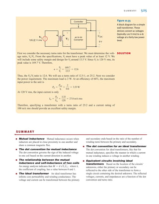
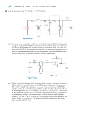
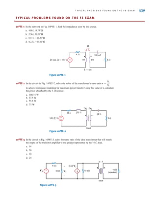
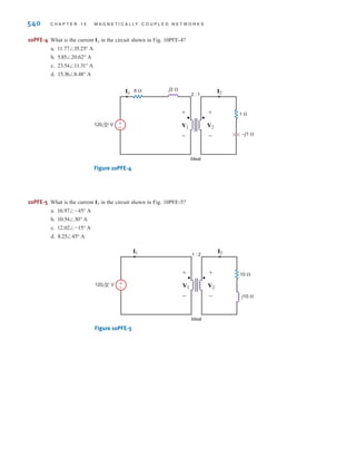

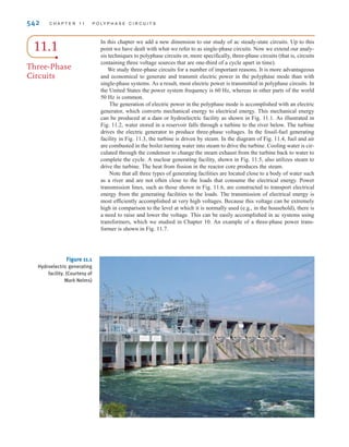
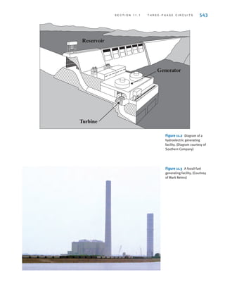
![546 C H A P T E R 1 1 P O LY P H A S E C I R C U I T S
Our double-subscript notation is exactly the same as that employed in the earlier
chapters; that is, means the voltage at point a with respect to point n. We will also
employ the double-subscript notation for currents; that is, Ian is used to represent the cur-
rent from a to n. However, we must be very careful in this case to describe the precise path,
since in a circuit there will be more than one path between the two points. For example, in
the case of a single loop the two possible currents in the two paths will be 180° out of phase
with each other.
The preceding phasor voltages can be expressed in the time domain as
11.2
These time functions are shown in Fig. 11.8b.
Finally, let us examine the instantaneous power generated by a three-phase system.
Assume that the voltages in Fig. 11.8 are
11.3
If the load is balanced, the currents produced by the sources are
11.4
The instantaneous power produced by the system is
11.5
Using the trigonometric identity,
11.6
Eq. (11.5) becomes
11.7
which can be written as
11.8
There exists a trigonometric identity that allows us to simplify the preceding expression.
The identity, which we will prove later using phasors, is
11.9
If we employ this identity, the expression for the power becomes
11.10
p(t) = 3
V
mIm
2
cos W
cos + cos( - 120°) + cos( + 120°) = 0
+ cos(2t - - 120°) + cos(2t - + 120°)D
p(t) =
V
mIm
2
C3 cos + cos(2t - )
+ cos(2t - - 240°) + cos + cos(2t - - 480°)D
p(t) =
V
mIm
2
Ccos + cos(2t - ) + cos
cos cos =
1
2
Ccos( - ) + cos( + )D
+ cos(t - 240°) cos(t - - 240°)]
= V
mIm[cost cos(t - ) + cos(t - 120°) cos(t - - 120°)
p(t) = pa(t) + pb(t) + pc(t)
ic(t) = Im cos(t - - 240°) A
ib(t) = Im cos(t - - 120°) A
ia(t) = Im cos(t - ) A
vcn(t) = V
m cos(t - 240°) V
vbn(t) = V
m cos(t - 120°) V
van(t) = V
m cost V
vcn(t) = 12012 cos(t - 240°) V
vbn(t) = 12012 cos(t - 120°) V
van(t) = 12012 cost V
Van
irwin11_541-576hr.qxd 6-08-2010 15:11 Page 546](https://image.slidesharecdn.com/basic-engineering-circuit-analysis-10th-irwin-220801002926-2b111212/85/basic-engineering-circuit-analysis-10th-Irwin-pdf-571-320.jpg)
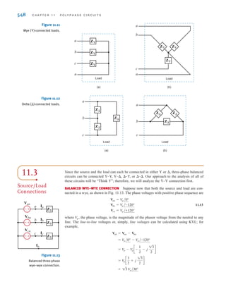
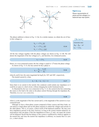
![S E C T I O N 1 1 . 3 S O U R C E / L O A D C O N N E C T I O N S 549
The phasor addition is shown in Fig. 11.14a. In a similar manner, we obtain the set of line-
to-line voltages as
11.14
All the line voltages together with the phase voltages are shown in Fig. 11.14b. We will
denote the magnitude of the line voltages as and therefore, for a balanced system,
11.15
Hence, in a wye-connected system, the line voltage is equal to times the phase voltage.
As shown in Fig. 11.13, the line current for the a phase is
11.16
where Ib and Ic have the same magnitude but lag Ia by 120° and 240°, respectively.
The neutral current In is then
11.17
Since there is no current in the neutral, this conductor could contain any impedance or it
could be an open or a short circuit, without changing the results found previously.
As illustrated by the wye–wye connection in Fig. 11.13, the current in the line connecting
the source to the load is the same as the phase current flowing through the impedance ZY.
Therefore, in a wye–wye connection,
11.18
where is the magnitude of the line current and is the magnitude of the current in a wye-
connected load.
Although we have a three-phase system composed of three sources and three loads, we
can analyze a single phase and use the phase sequence to obtain the voltages and currents in
the other phases. This is, of course, a direct result of the balanced condition. We may even
have impedances present in the lines; however, as long as the system remains balanced, we
need analyze only one phase. If the line impedances in lines a, b, and c are equal, the system
will be balanced. Recall that the balance of the system is unaffected by whatever appears in
the neutral line, and since the neutral line impedance is arbitrary, we assume that it is zero
(i.e., a short circuit).
IY
IL
IL = IY
In = AIa + Ib + IcB = 0
Ia =
Van
ZY
=
V
p /0°
ZY
13
V
L = 13 V
p
V
L,
Vca = 13 V
p /-210°
Vbc = 13 V
p /-90°
Vab = 13 V
p /30°
Figure 11.14
Phasor representation of
phase and line voltages in a
balanced wye–wye system.
Vab
Vbn
Vcn
Van
Vab
Van
Vbn
Vbc
Vcn
Vca
30° 30°
(a) (b)
Conversion rules:
Vab = 23 Van
/Vab = /Van + 30°
[ h i n t ]
irwin11_541-576hr.qxd 6-08-2010 15:11 Page 549](https://image.slidesharecdn.com/basic-engineering-circuit-analysis-10th-irwin-220801002926-2b111212/85/basic-engineering-circuit-analysis-10th-Irwin-pdf-574-320.jpg)
![550 C H A P T E R 1 1 P O LY P H A S E C I R C U I T S
EXAMPLE
11.1
SOLUTION
EXAMPLE
11.2
SOLUTION
An abc-sequence three-phase voltage source connected in a balanced wye has a line volt-
age of We wish to determine the phase voltages.
The magnitude of the phase voltage is given by the expression
The phase relationships between the line and phase voltages are shown in Fig. 11.14. From
this figure we note that
The magnitudes of these voltages are quite common, and one often hears that the electric
service in a building, for example, is three-phase 208/120 V rms.
Vcn = 120/+60° V rms
Vbn = 120/-180° V rms
Van = 120/-60° V rms
= 120 V rms
V
p =
208
13
Vab = 208/-30° V rms.
A three-phase wye-connected load is supplied by an abc-sequence balanced three-phase
wye-connected source with a phase voltage of 120 V rms. If the line impedance and load
impedance per phase are 1+j1 and 20+j10 , respectively, we wish to determine the
value of the line currents and the load voltages.
The phase voltages are
The per-phase circuit diagram is shown in Fig. 11.15. The line current for the a phase is
The load voltage for the a phase, which we call is
= 113.15/-1.08° V rms
VAN = A5.06/-27.65°B(20 + j10)
VAN,
= 5.06/-27.65° A rms
IaA =
120/0°
21 + j11
Vcn = 120/+120° V rms
Vbn = 120/-120° V rms
Van = 120/0° V rms
Figure 11.15
Per-phase circuit diagram
for the problem in
Example 11.2.
±
–
VAN
Van
IaA
N
n
a A
20 ⍀
1 ⍀ j1 ⍀
j10 ⍀
The phase of
Van = /Van = /Vab - 30°
[ h i n t ]
/IcC = /IaA + 120°
/IbB = /IaA - 120°
[ h i n t ]
irwin11_541-576hr.qxd 6-08-2010 15:11 Page 550](https://image.slidesharecdn.com/basic-engineering-circuit-analysis-10th-irwin-220801002926-2b111212/85/basic-engineering-circuit-analysis-10th-Irwin-pdf-575-320.jpg)
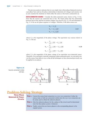
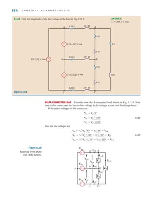
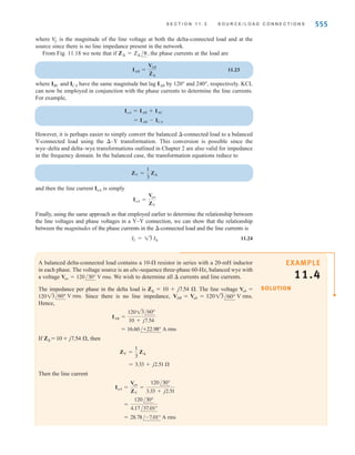
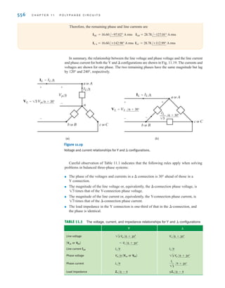
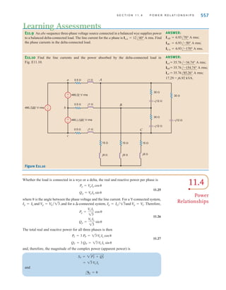
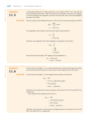
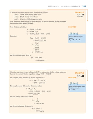
![S E C T I O N 1 1 . 4 P O W E R R E L A T I O N S H I P S 559
EXAMPLE
11.7
SOLUTION
A balanced three-phase source serves three loads, as follows:
Load 1: 24 kW at 0.6 lagging power factor
Load 2: 10 kW at unity power factor
Load 3: 12 k at 0.8 leading power factor
If the line voltage at the loads is 208 V rms at 60 Hz, we wish to determine the line current and
the combined power factor of the loads.
From the data we find that
Therefore,
and the combined power factor is
= 0.869 lagging
pfload = cos29.63°
IL = 139.23 A rms
=
50,160
20813
IL =
@Sload @
13 V
L
= 50,160/29.63° VA
Sload = 43,600 + j24,800
S3 = 12,000/-36.9° = 9600 - j7200
S2 = 10,000 + j0
S1 = 24,000 + j32,000
VA
The sum of three complex
powers;
Sload = S1 + S2 + S3
[ h i n t ]
EXAMPLE
11.8
SOLUTION
Given the three-phase system in Example 11.7, let us determine the line voltage and power
factor at the source if the line impedance is Zline = 0.05 + j0.02 .
The complex power absorbed by the line impedances is
The complex power delivered by the source is then
The line voltage at the source is then
and the power factor at the source is
= 0.873 lagging
pfS = cos29.17°
= 220.87 V rms
V
LS
=
SS
13 IL
= 53,264/29.17° VA
= 43,600 + j24,800 + 2908 + j1163
SS = Sload + Sline
= 2908 + j1163 VA
Sline = 3ARlineI2
L + jXlineI2
LB
Recall that the complex power
for all three lines is
Sline = 3I2
LZline
[ h i n t ]
irwin11_541-576hr.qxd 6-08-2010 15:11 Page 559](https://image.slidesharecdn.com/basic-engineering-circuit-analysis-10th-irwin-220801002926-2b111212/85/basic-engineering-circuit-analysis-10th-Irwin-pdf-584-320.jpg)
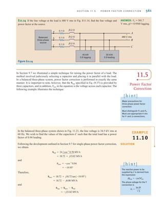
![S E C T I O N 1 1 . 5 P O W E R F A C T O R C O R R E C T I O N 561
E11.14 If the line voltage at the load is 480 V rms in Fig. E11.14, find the line voltage and
power factor at the source.
ANSWER: VL = 501.7
V rms, pf = 0.9568 lagging.
a
b
c
40 kW
0.8 lagging
Balanced
three-phase
source
0.1 j0.2
0.1 j0.2
0.1 j0.2
A
B
C
30 kVA
0.9 leading
+
–
480 V rms
In Section 9.7 we illustrated a simple technique for raising the power factor of a load. The
method involved judiciously selecting a capacitor and placing it in parallel with the load.
In a balanced three-phase system, power factor correction is performed in exactly the same
manner. It is important to note, however, that the Scap specified in Eq. (9.37) is provided by
three capacitors, and in addition, in the equation is the voltage across each capacitor. The
following example illustrates the technique.
Vrms
11.5
Power Factor
Correction
Major precautions for
three-phase power factor
correction:
Must distinguish PT and PP.
Must use appropriate V rms
for Y- and -connections.
[ h i n t ]
EXAMPLE
11.10
SOLUTION
In the balanced three-phase system shown in Fig. 11.21, the line voltage is 34.5 kV rms at
60 Hz. We wish to find the values of the capacitors C such that the total load has a power
factor of 0.94 leading.
Following the development outlined in Section 9.7 for single-phase power factor correction,
we obtain
and
Therefore,
and
= -j21.82 MVA
Scap = Snew - Sold
= 18.72 - j6.80 MVA
Snew = 18.72 + j18.72 tan(-19.95°)
= -19.95°
new = -cos-1
0.94
= 18.72 + j15.02 MVA
Sold = 24/cos-1
0.78 MVA
Figure E11.14
The reactive power to be
supplied by C is derived from
the expression
The phase voltage for the Y
connection is
VY =
34.5k
13
jQcap = -jCV2
rms
[ h i n t ]
irwin11_541-576hr.qxd 6-08-2010 15:11 Page 561](https://image.slidesharecdn.com/basic-engineering-circuit-analysis-10th-irwin-220801002926-2b111212/85/basic-engineering-circuit-analysis-10th-Irwin-pdf-586-320.jpg)
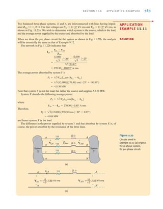
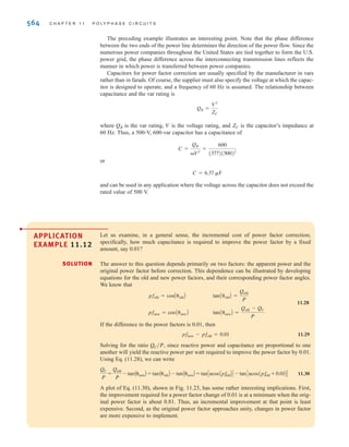
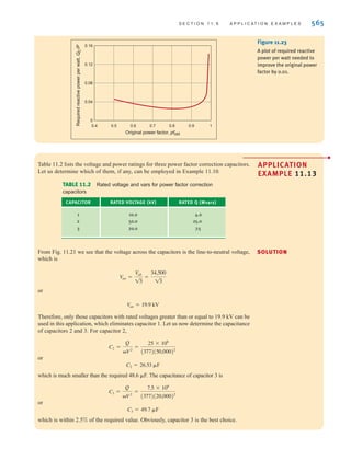
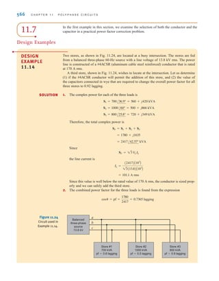
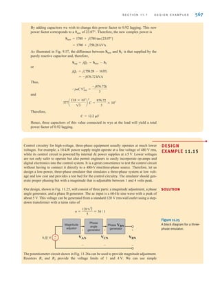
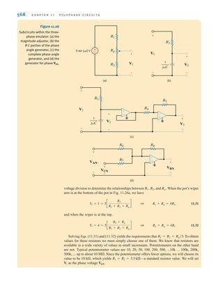
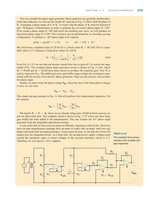
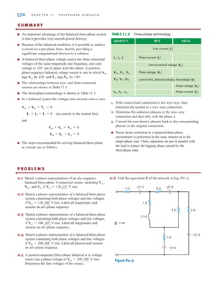
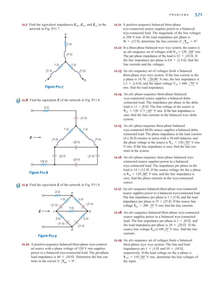
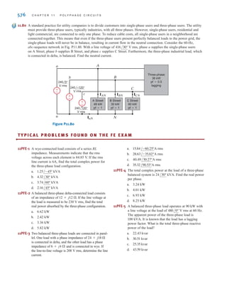

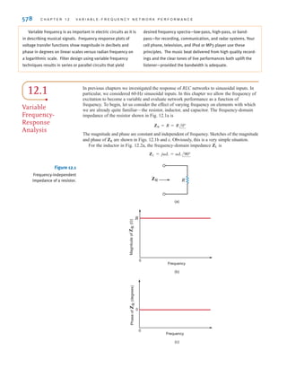
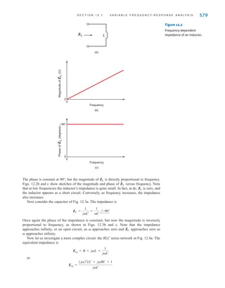
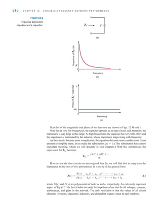
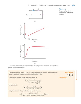
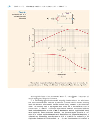
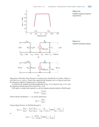
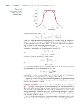
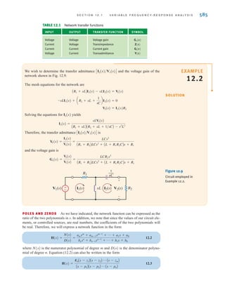
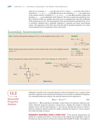
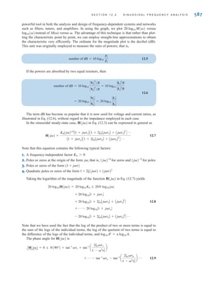
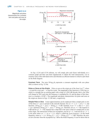
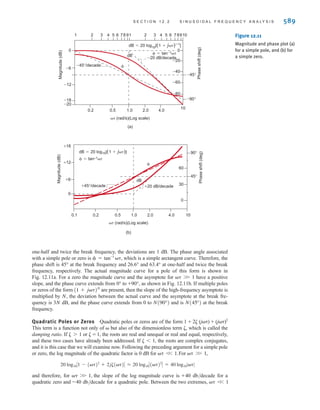
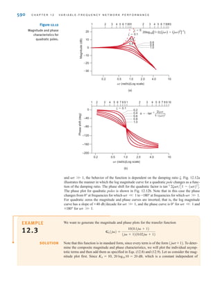
![and the behavior of the function is dependent on the damping ratio . Fig. 12.12a
illustrates the manner in which the log magnitude curve for a quadratic pole changes as a func-
tion of the damping ratio. The phase shift for the quadratic factor is
The phase plot for quadratic poles is shown in Fig. 12.12b. Note that in this case the phase
changes from 0° at frequencies for which to –180° at frequencies for which
For quadratic zeros the magnitude and phase curves are inverted; that is, the log magnitude
curve has a slope of +40 db/decade for and the phase curve is 0° for and
for W 1.
+180°
V 1
W 1,
W 1.
V 1
tan-1
2兾C1 - ()2
D.
W 1,
590 C H A P T E R 1 2 V A R I A B L E - F R E Q U E N C Y N E T W O R K P E R F O R M A N C E
0.2 0.5 1.0 2.0 4.0 10
(rad/s)(Log scale)
0
–200
–160
–120
Phase
shift
(deg)
(b)
10
9
8
7
6
5
4
3
2
1
9
8
7
6
5
4
3
2
1
–40
–80
=0.1
=–tan–1
—
2
1–()2
0.2
0.4
0.6
0.8
1.0
=0
0.2 0.5 1.0 2.0 4.0 10
(rad/s)(Log scale)
20
–30
–20
–10
Magnitude
(dB)
(a)
10
9
8
7
6
5
4
3
2
1
9
8
7
6
5
4
3
2
1
10
0
20log10|[1±2(j)+(j)2
]–1
|
0.2
0.4 0.6
0.8
1.0
=0.1
Figure 12.12
Magnitude and phase
characteristics for
quadratic poles.
EXAMPLE
12.3
SOLUTION
We want to generate the magnitude and phase plots for the transfer function
Note that this function is in standard form, since every term is of the form (j + 1). To deter-
mine the composite magnitude and phase characteristics, we will plot the individual asymp-
totic terms and then add them as specified in Eqs. (12.8) and (12.9). Let us consider the mag-
nitude plot first. Since K0=10, which is a constant independent of
20 log10 10 = 20 dB,
Gv(j) =
10(0.1j + 1)
(j + 1)(0.02j + 1)
irwin12_577-666hr.qxd 6-08-2010 15:14 Page 590](https://image.slidesharecdn.com/basic-engineering-circuit-analysis-10th-irwin-220801002926-2b111212/85/basic-engineering-circuit-analysis-10th-Irwin-pdf-615-320.jpg)