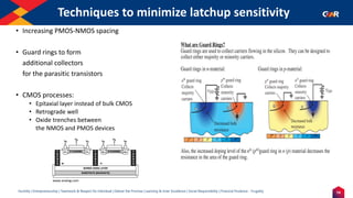
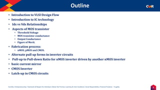
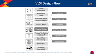
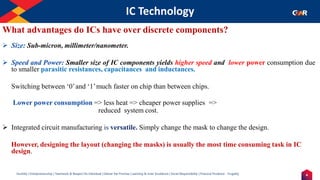
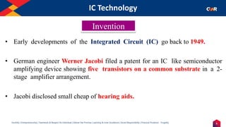
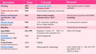
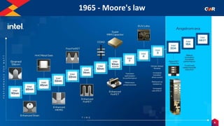
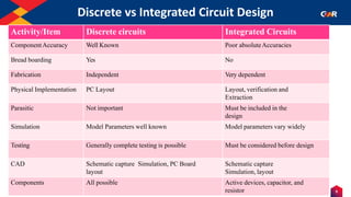
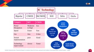
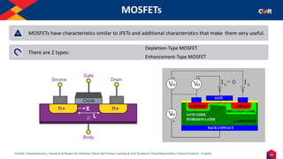
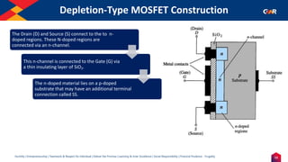
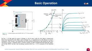
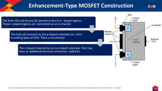
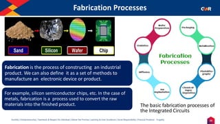
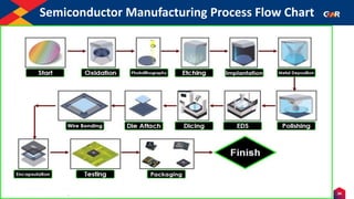
This document presents an introduction to VLSI design and integrated circuit (IC) technology, highlighting key concepts such as MOS transistor properties, fabrication processes, and historical developments in IC design. It discusses advantages of ICs over discrete components, including size and efficiency, and covers the fundamental principles of MOSFETs and their applications. Additionally, the document outlines the steps involved in IC fabrication, emphasizing processes like oxidation, photolithography, and ion implantation.


![37
Humility | Entrepreneurship | Teamwork & Respect for Individual | Deliver the Promise | Learning & Inner Excellence | Social Responsibility | Financial Prudence - Frugality
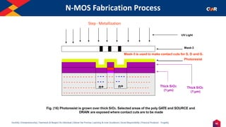
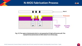
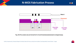
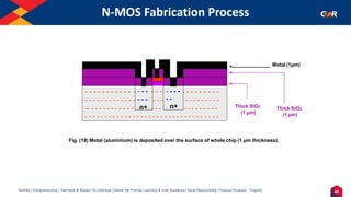
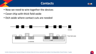
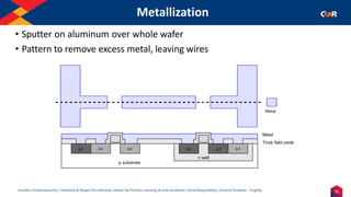
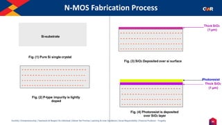
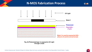
N-MOS Fabrication Process
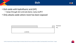
Fig. (6) Etching [HF acid is used] will remove SiO2 layer
which is in direct contact with etching solution
Thick SiO2
(1 µm)
- - - - - - - - - - - - - - - - - - - - - - - - - - - - - - -
- - - - - - - - - - - - - - - - - - - - - - - - - - - - - - - - - -
-- - - - - - - - - - - - - - - - - - - - - - - - - - - - - - - - -
- - - - - - - - - - - - - - - - - - - - - - - - - - - - - - - - - -
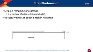
Fig. (7) unpolymerised photoresist is also etched away
[using H2SO4]
- - - - - - - - - - - - - - - - - - - - - - - - - - - - - - -
- - - - - - - - - - - - - - - - - - - - - - - - - - - - - - - - - -
-- - - - - - - - - - - - - - - - - - - - - - - - - - - - - - - - -
- - - - - - - - - - - - - - - - - - - - - - - - - - - - - - - - - -
Thick SiO2
(1 µm)](https://image.slidesharecdn.com/module-1-250127041003-398c0b5b/85/Basic-electrical-properties-of-MOSFET-circuits-pdf-37-320.jpg)