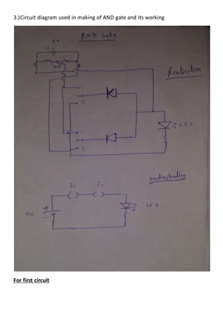
Aim
To understand the working of AND gate using p-n junction diodes and to design
a circuit of AND gate using diodes, LED, push button type toggle switches and
suitable resistances.
Introduction
AND gate is an Boolean operator based on the mathematical function of
multiplication.
It works on digital signals as its input which have only two states of voltages, low
as 0V and high as 5V.
AND gate consists of electonic circuit of p-n junction diodes having two input
digital signals which can take four different combinations on voltages, for each
combination of voltages there is a predefined output according to multiplication
rule.
Apparatus used
p-n junction diode (IN 4007)
Circuit board
Wires
9V battery and battery connector
LED (5mm, 1.5V)
Resistors
Push button type toggle switch
Push buttons
Theory and working
1.)Working of p-n junction diode in forward and reverse biasing
2.)Understanding the functioning of AND gate and its realisation
Realisation of AND gate
3.)Circuit diagram used in making of AND gate and its working
For first circuit
When the push button is in ‘released state’ then terminal ‘2’ is connected to
terminal ‘3’, when push button is in ‘active or pressed’ then terminal ‘2’ is
connected to terminal ‘1’.
The push button connected to first diode is ‘button 1’ and the other one is
‘button 2’.
When ‘button 1’ is released and ‘button 2’ is released then it is equivalent to
A(0), B(0). In this state, first and second diodes are forward biased, current
flows through diodes to negative terminal of battery but does not flow through
LED.
When ‘button 1’ is pressed and ‘button 2’ is released then it is equivalent to
A(1), B(0). In this state, first diode is reverse biased and second diode is forward
biased, current flows through second diode to negative of battery but does not
flows through LED.
When ‘button 2’ is pressed and ‘button 1’ is released then it is equivalent to
A(0), B(1). In this state, first diode is forward biased and second diode is reverse
biased, current flows through first diode to negative of battery but does not
flows through LED.
When ‘button 1’ is pressed and also ‘button 2’ is pressed then it is equivalent to
A(1), B(1). In this state, first diode and second diode are reverse biased, current
flows through LED.
Conclusion
The output of AND gate for four combinations of inputs clearly shows the
expected output according to the truth table.
Sources of errors
Write yourself
Precautions
Do not connect any electronic component without resistance in series, it can
burn the component.
Bibliography
NCERT textbook of class 12
Physics by S.L.Arora
Circuits available on internet

And gate

  • 1.
    Aim To understand theworking of AND gate using p-n junction diodes and to design a circuit of AND gate using diodes, LED, push button type toggle switches and suitable resistances.
  • 2.
    Introduction AND gate isan Boolean operator based on the mathematical function of multiplication. It works on digital signals as its input which have only two states of voltages, low as 0V and high as 5V. AND gate consists of electonic circuit of p-n junction diodes having two input digital signals which can take four different combinations on voltages, for each combination of voltages there is a predefined output according to multiplication rule.
  • 3.
    Apparatus used p-n junctiondiode (IN 4007) Circuit board Wires 9V battery and battery connector LED (5mm, 1.5V) Resistors Push button type toggle switch Push buttons
  • 4.
    Theory and working 1.)Workingof p-n junction diode in forward and reverse biasing
  • 5.
    2.)Understanding the functioningof AND gate and its realisation
  • 8.
  • 9.
    3.)Circuit diagram usedin making of AND gate and its working For first circuit
  • 10.
    When the pushbutton is in ‘released state’ then terminal ‘2’ is connected to terminal ‘3’, when push button is in ‘active or pressed’ then terminal ‘2’ is connected to terminal ‘1’. The push button connected to first diode is ‘button 1’ and the other one is ‘button 2’. When ‘button 1’ is released and ‘button 2’ is released then it is equivalent to A(0), B(0). In this state, first and second diodes are forward biased, current flows through diodes to negative terminal of battery but does not flow through LED. When ‘button 1’ is pressed and ‘button 2’ is released then it is equivalent to A(1), B(0). In this state, first diode is reverse biased and second diode is forward biased, current flows through second diode to negative of battery but does not flows through LED. When ‘button 2’ is pressed and ‘button 1’ is released then it is equivalent to A(0), B(1). In this state, first diode is forward biased and second diode is reverse biased, current flows through first diode to negative of battery but does not flows through LED. When ‘button 1’ is pressed and also ‘button 2’ is pressed then it is equivalent to A(1), B(1). In this state, first diode and second diode are reverse biased, current flows through LED.
  • 11.
    Conclusion The output ofAND gate for four combinations of inputs clearly shows the expected output according to the truth table. Sources of errors Write yourself Precautions Do not connect any electronic component without resistance in series, it can burn the component. Bibliography NCERT textbook of class 12 Physics by S.L.Arora Circuits available on internet