Downloaded 140 times


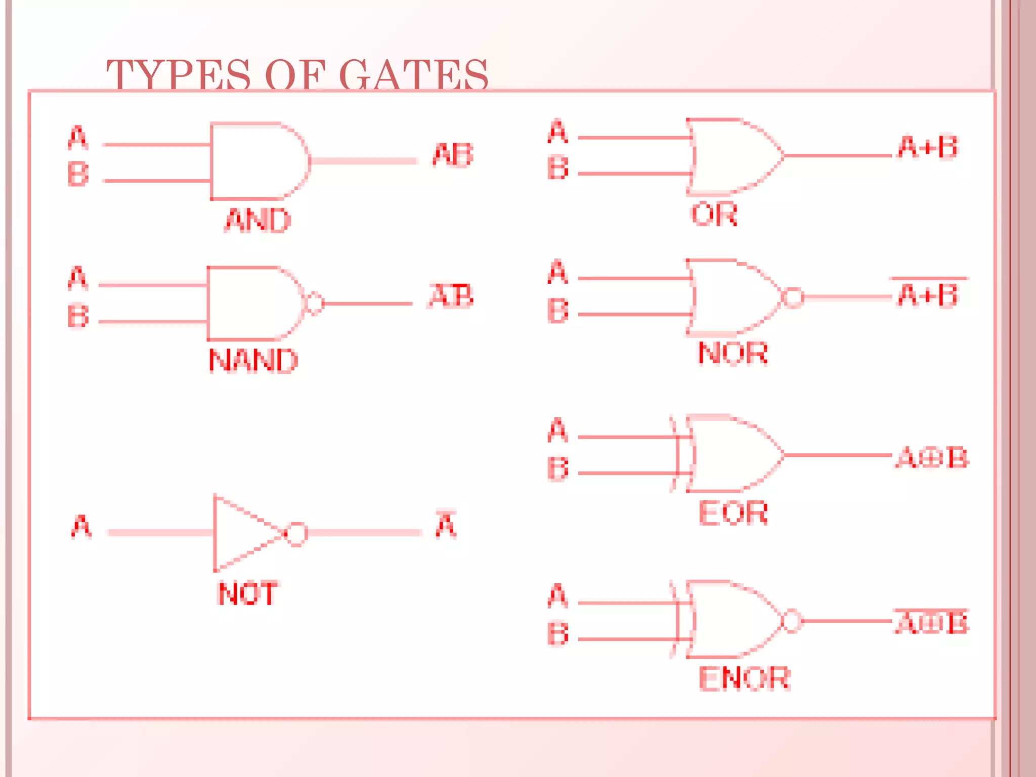


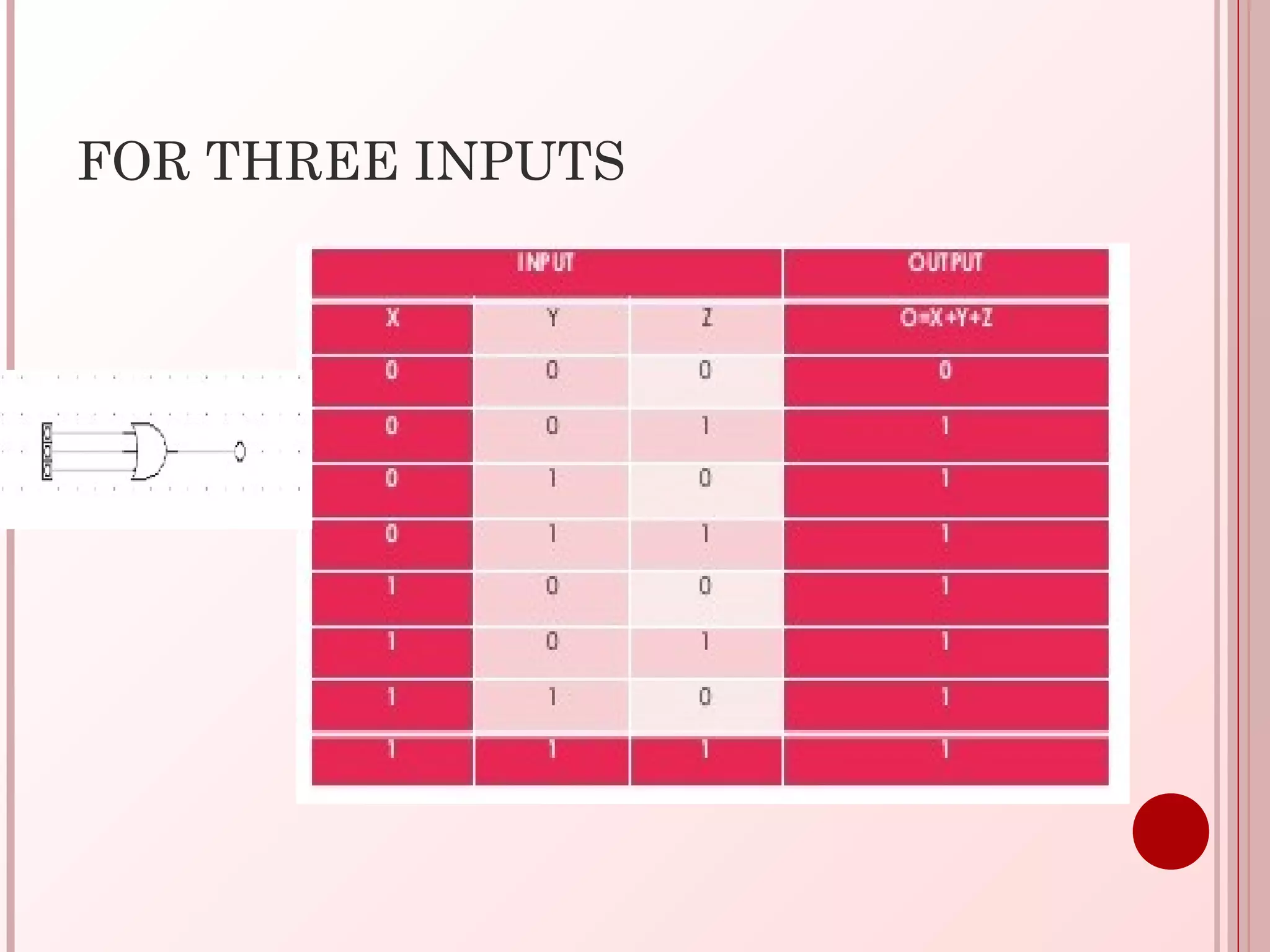


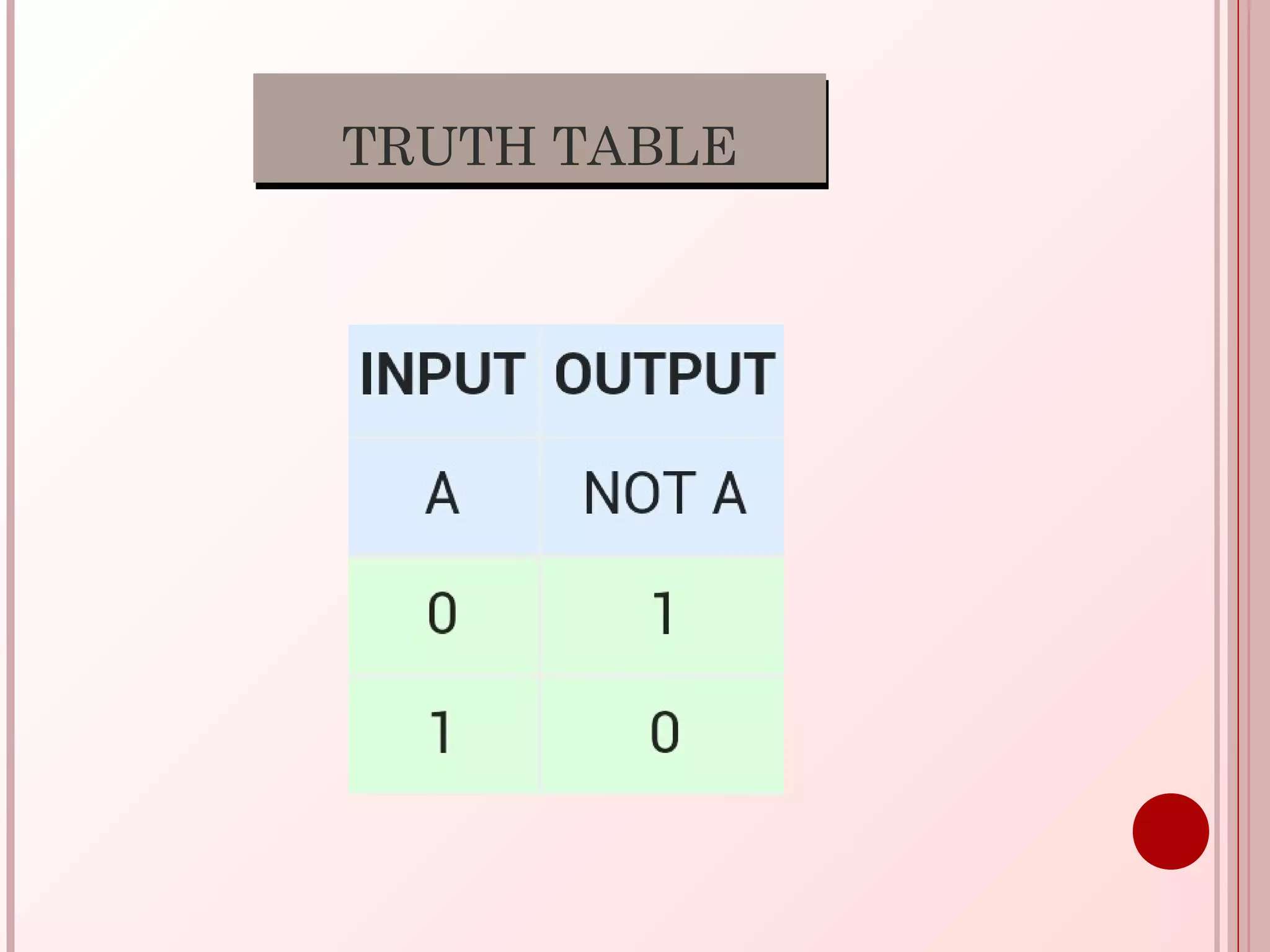


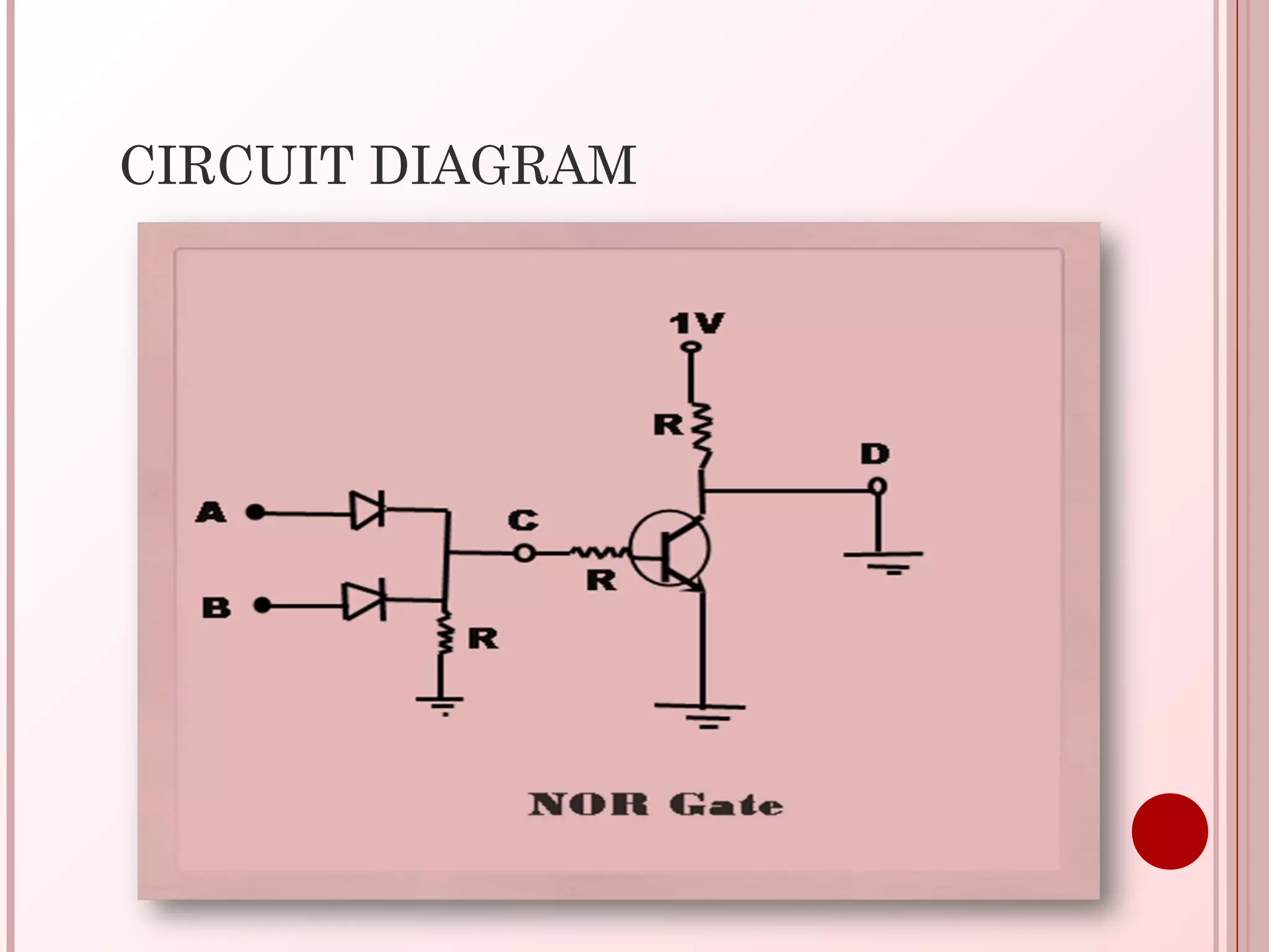


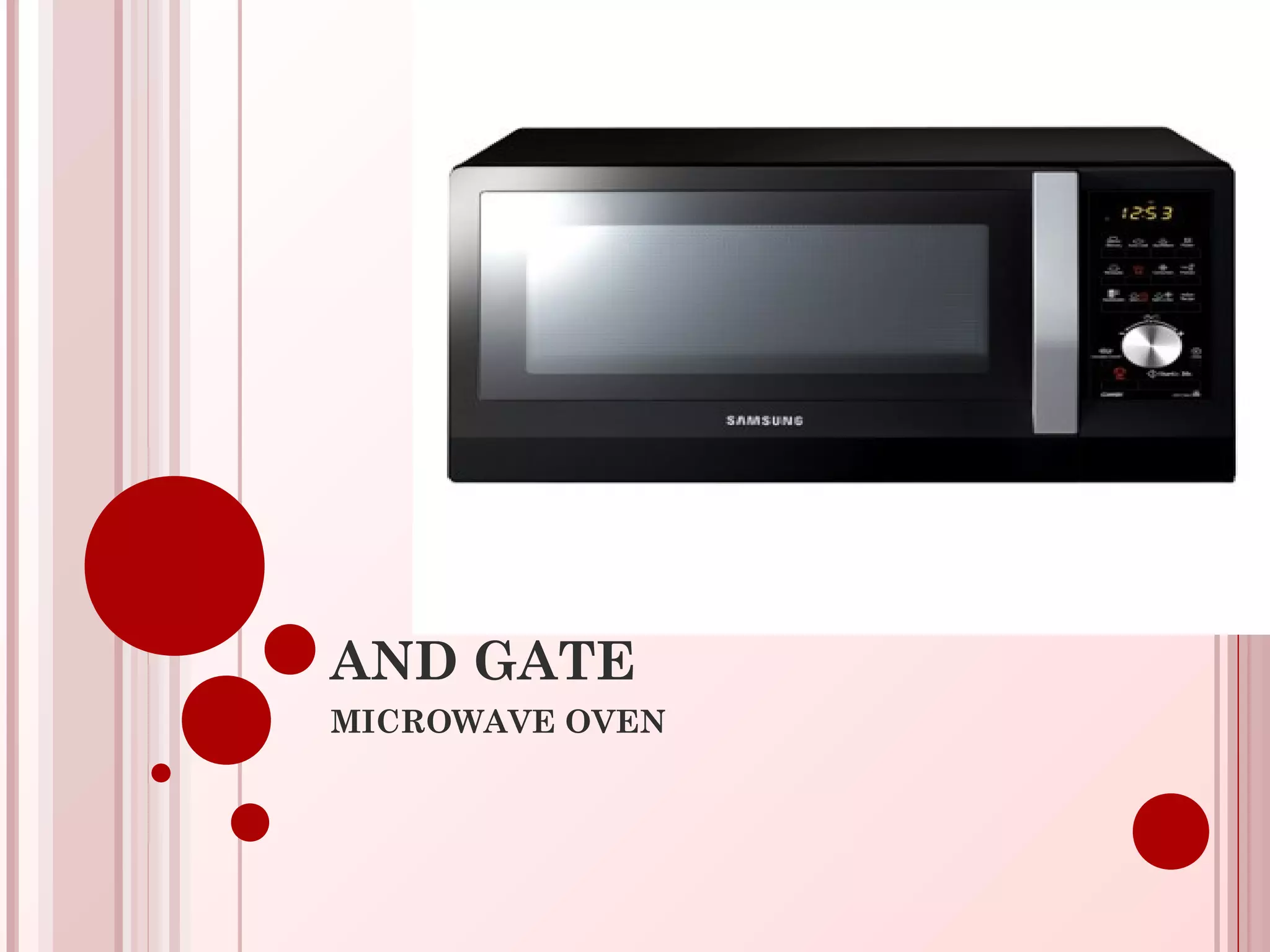

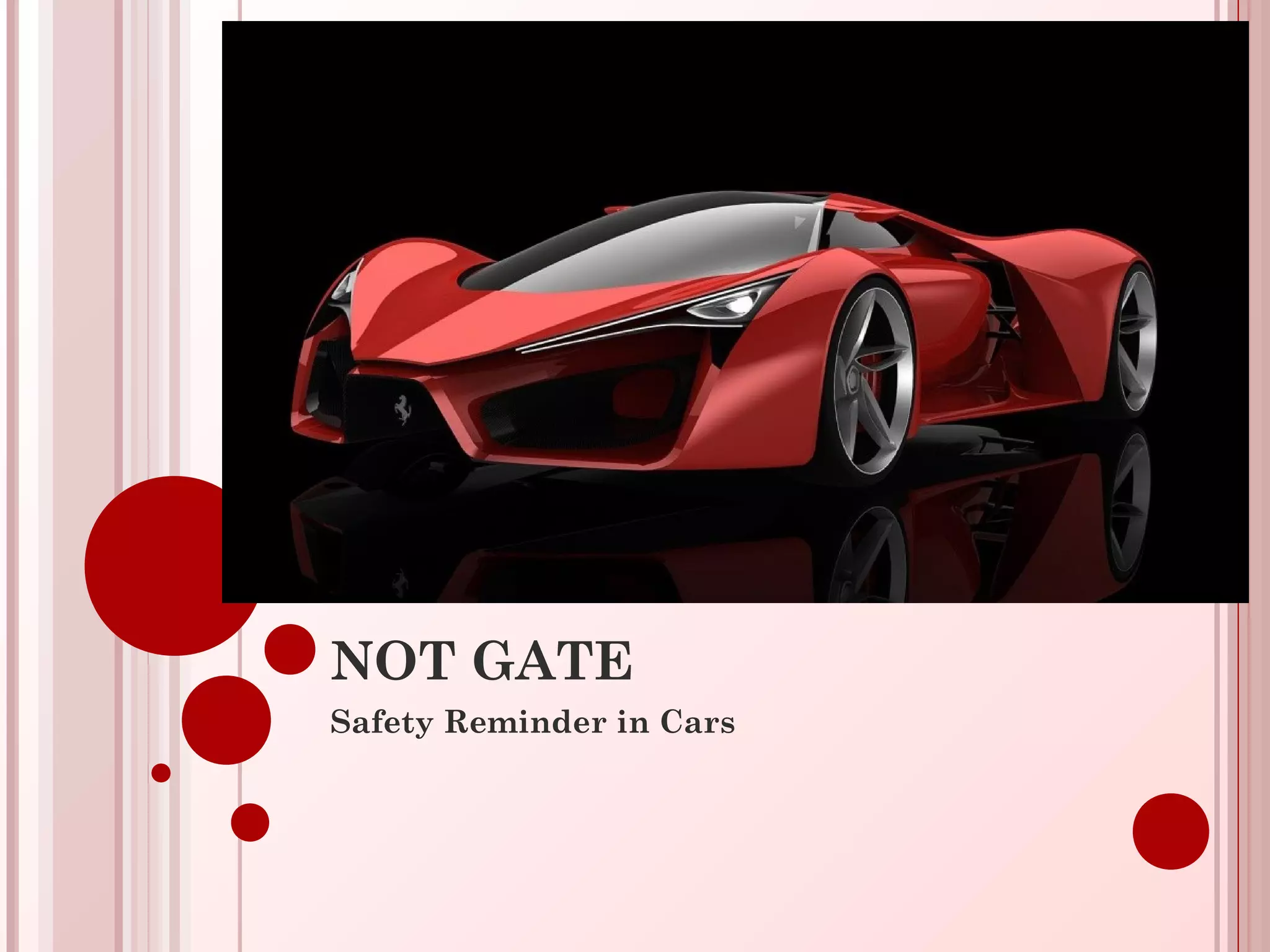


This document provides information about logic gates. It discusses the history of logic gates and binary systems. It then defines common logic gates like OR, AND, NOT, NAND, and NOR gates. For each gate, it provides the symbolic representation, truth table, and examples of how the gate works. It also discusses applications of each gate type in contexts like industrial plants, microwave ovens, car safety systems, freezers, and home security systems. The document is authored by six group members and contains detailed information about the key concepts and components of logic gates.