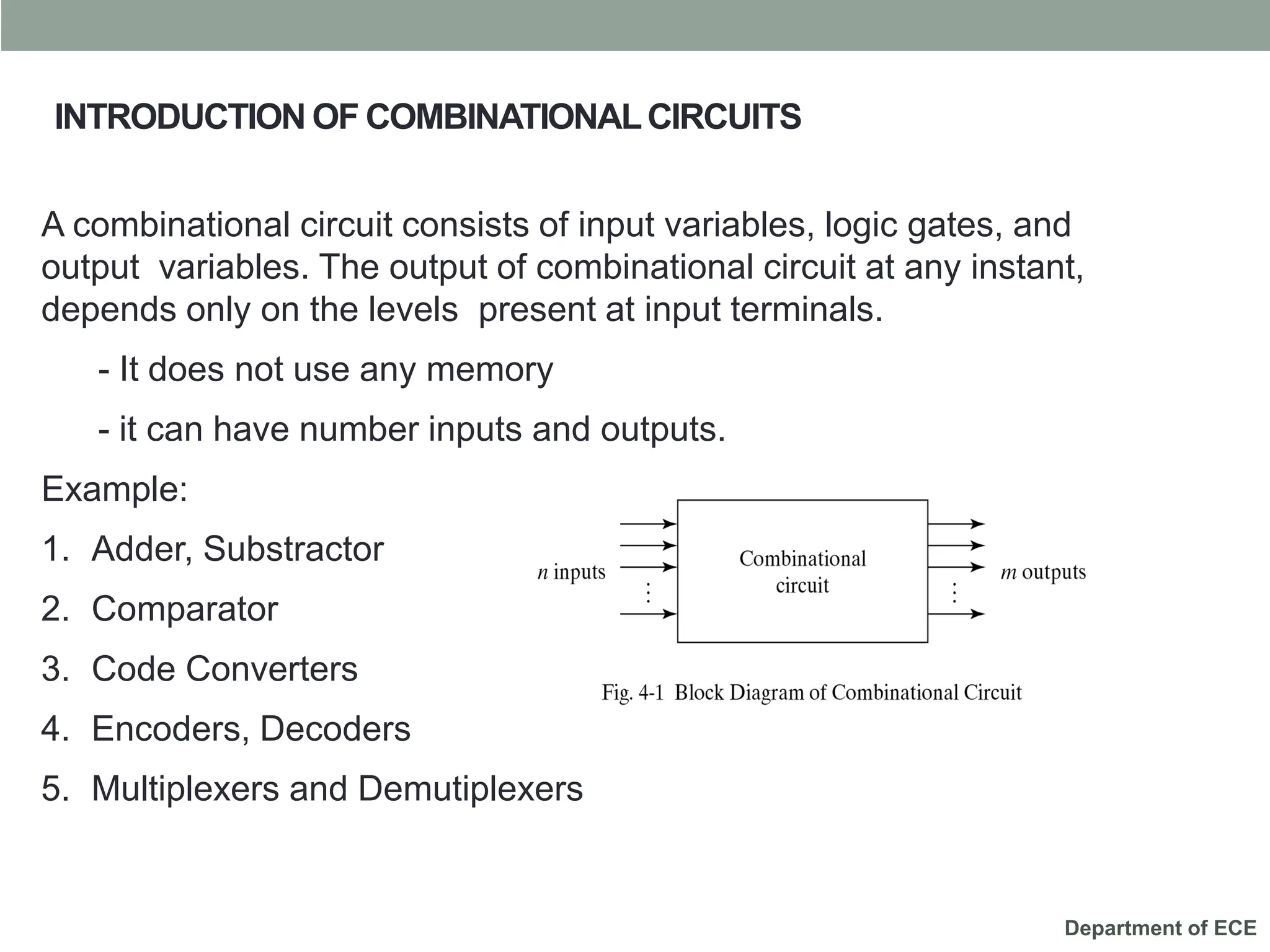
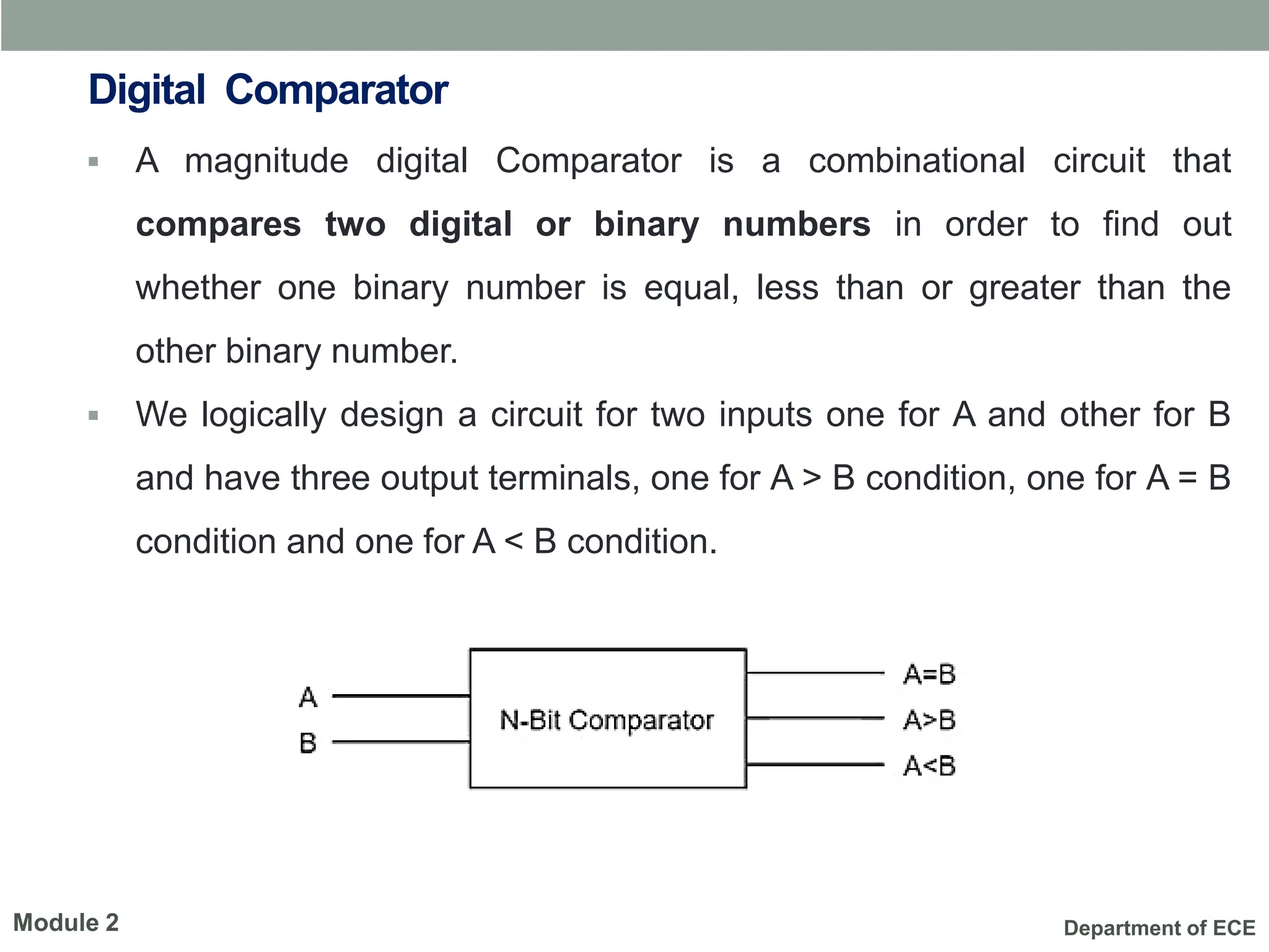
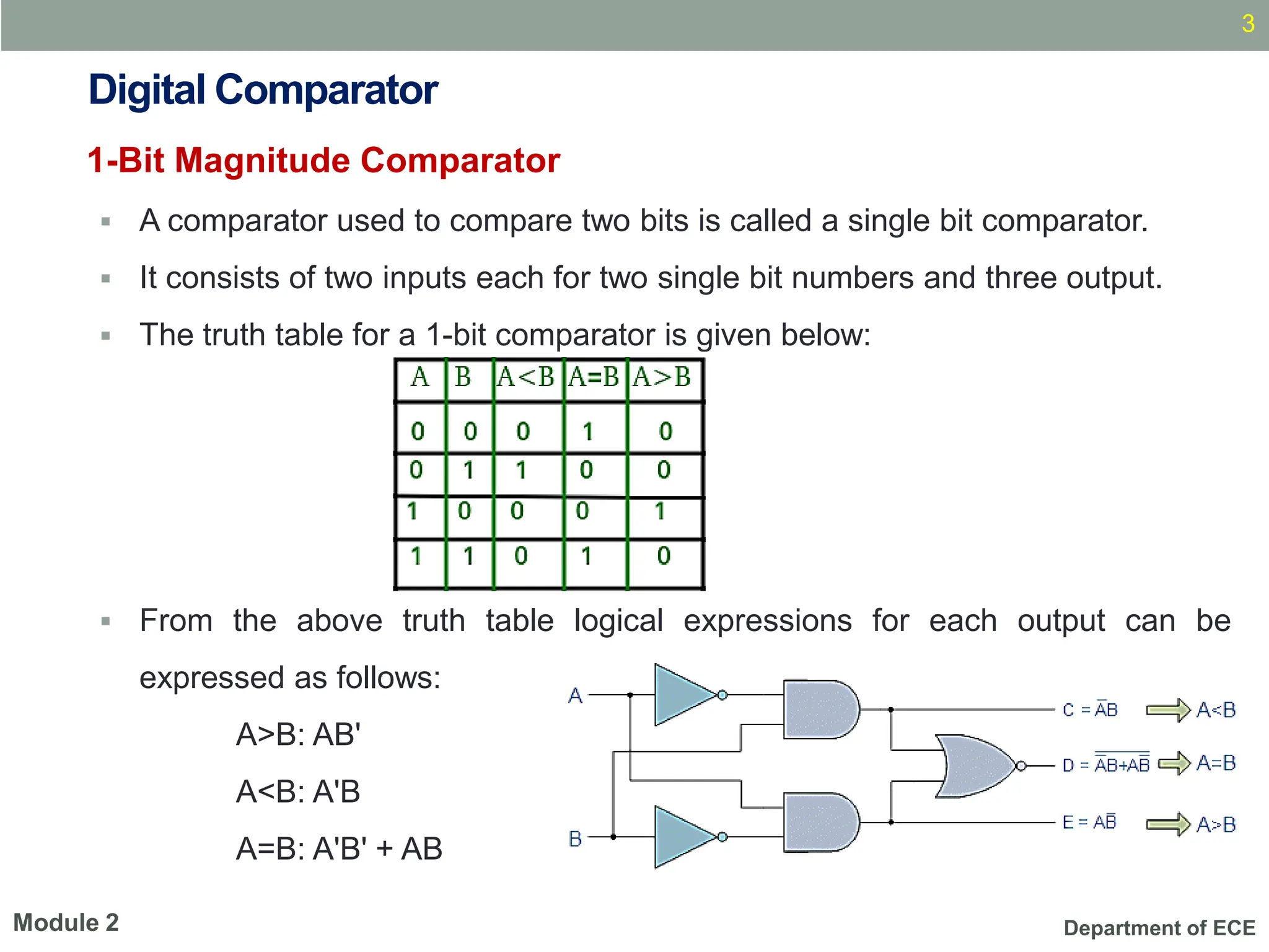
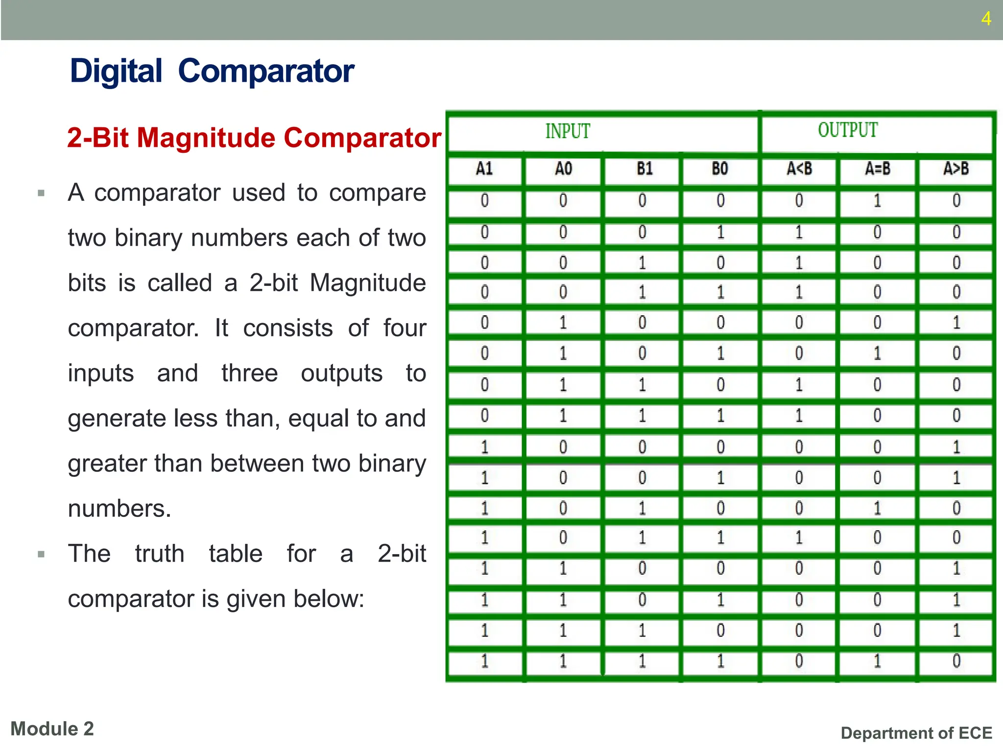
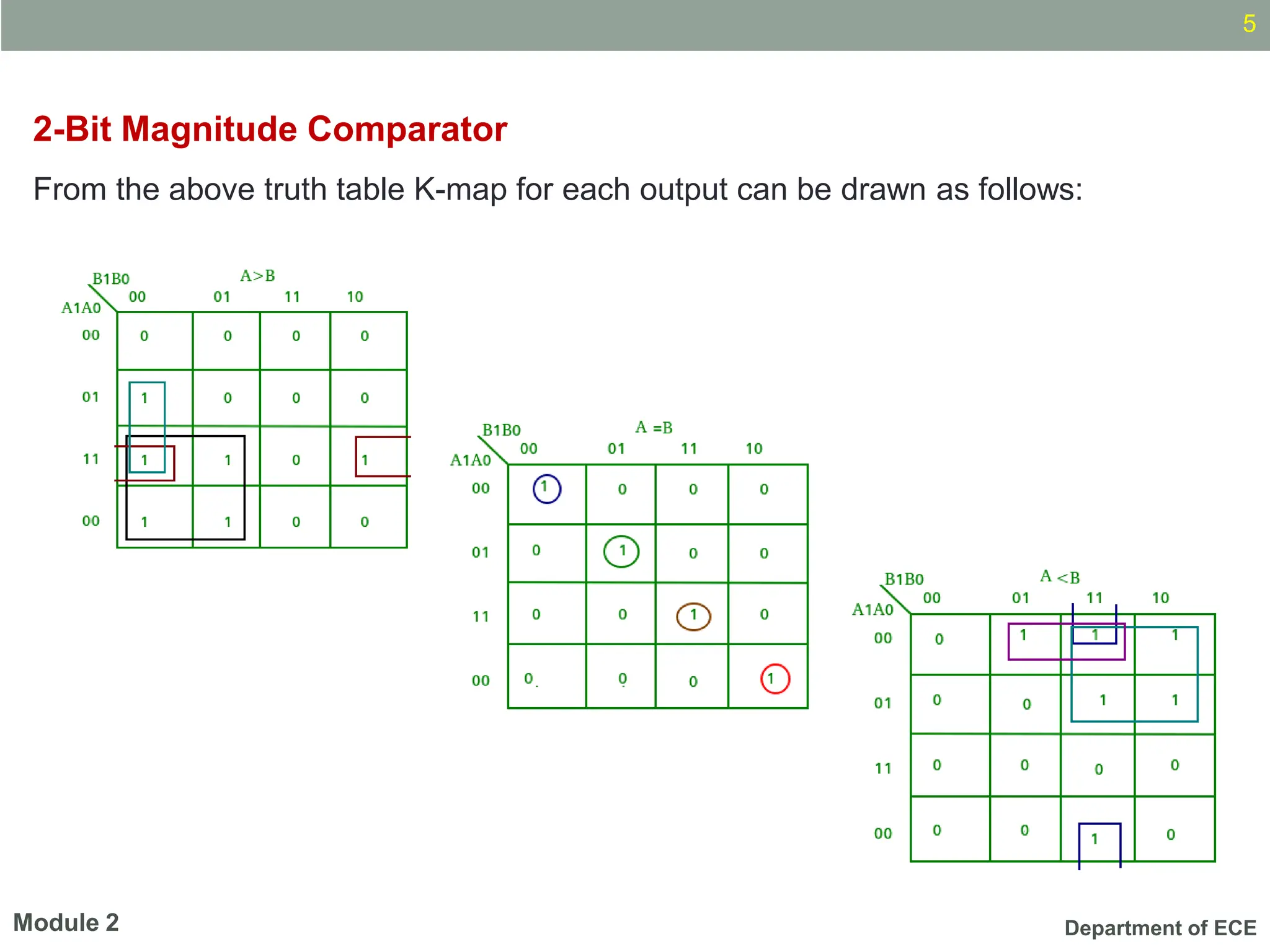
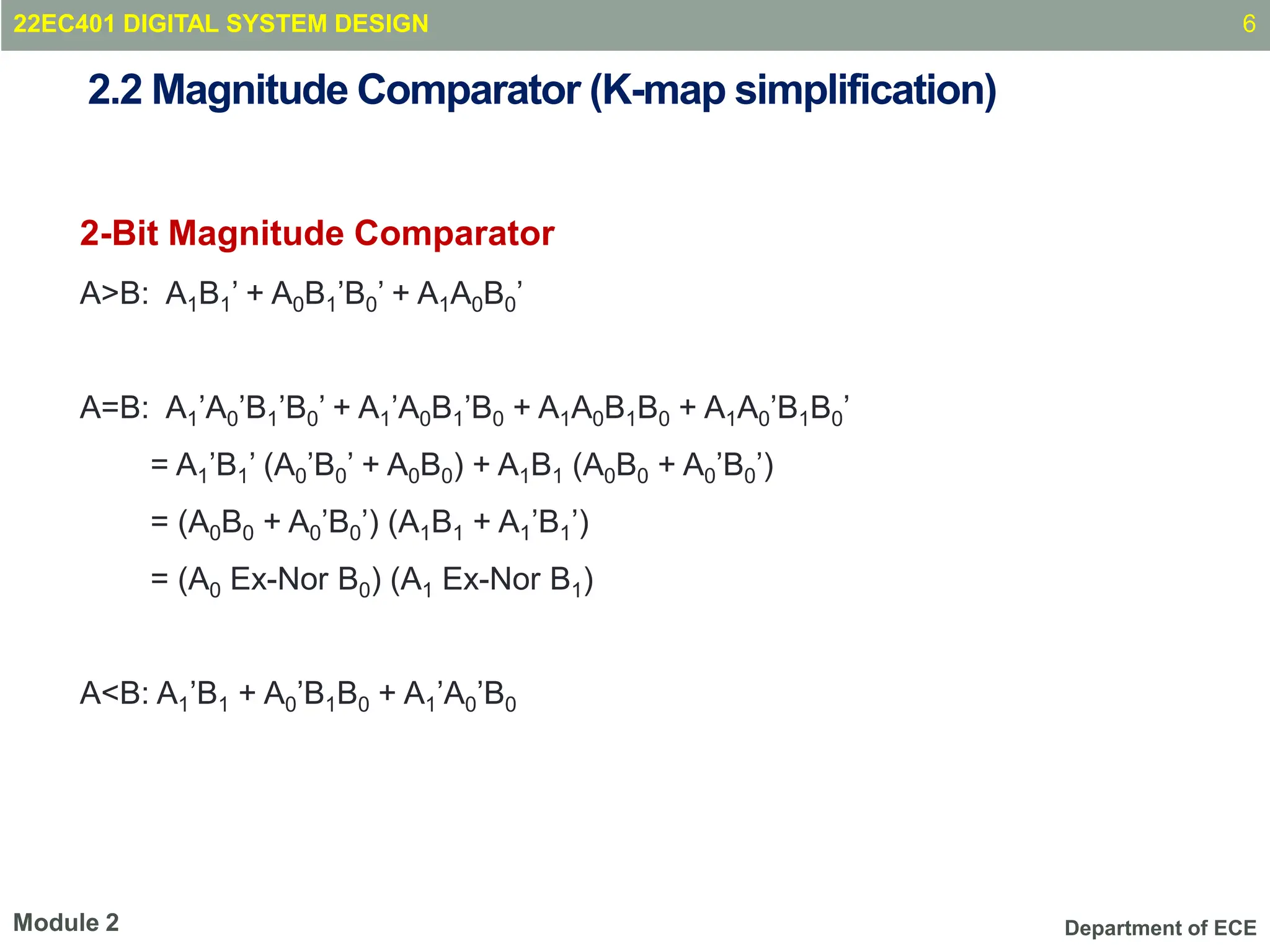
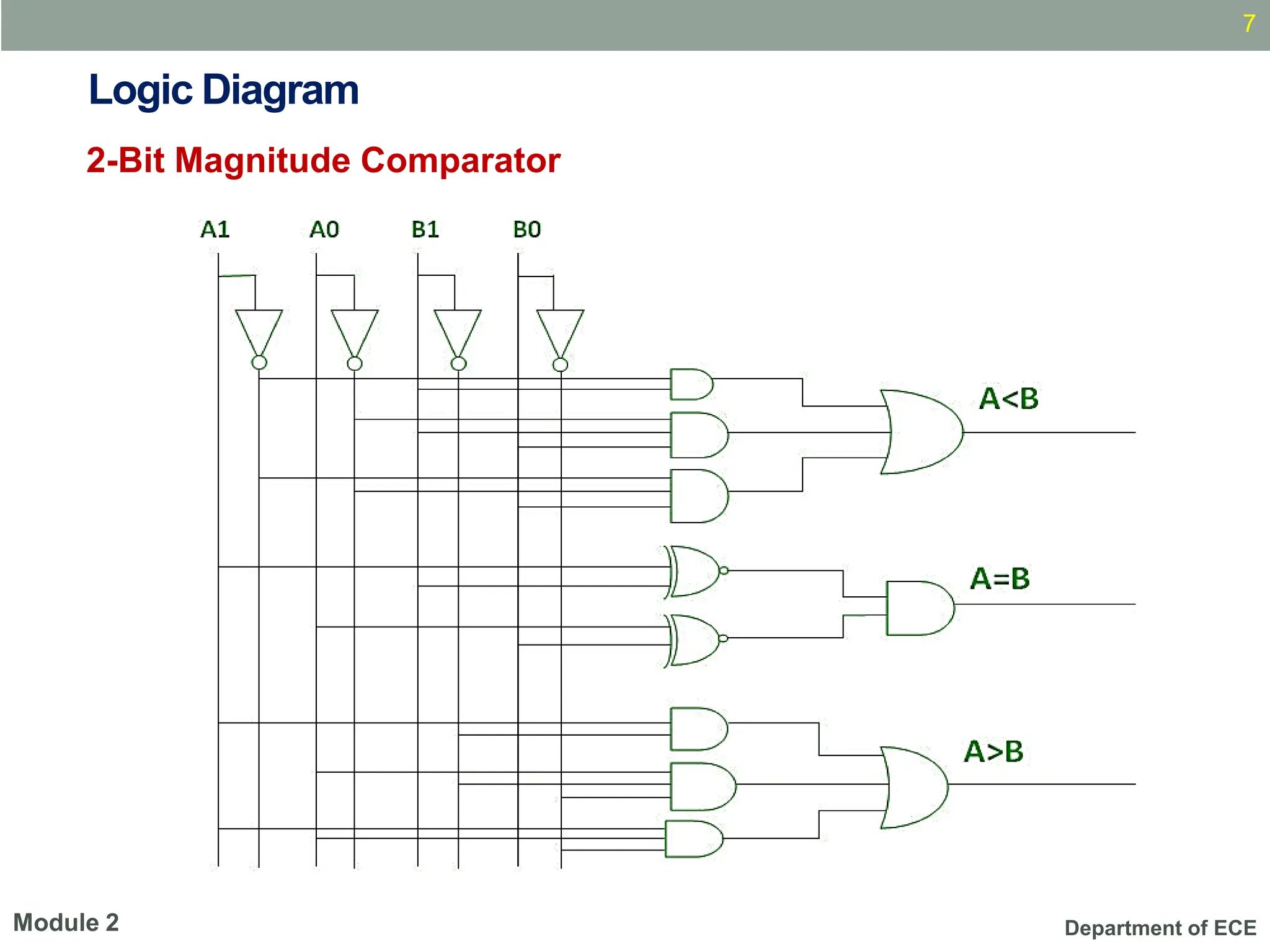
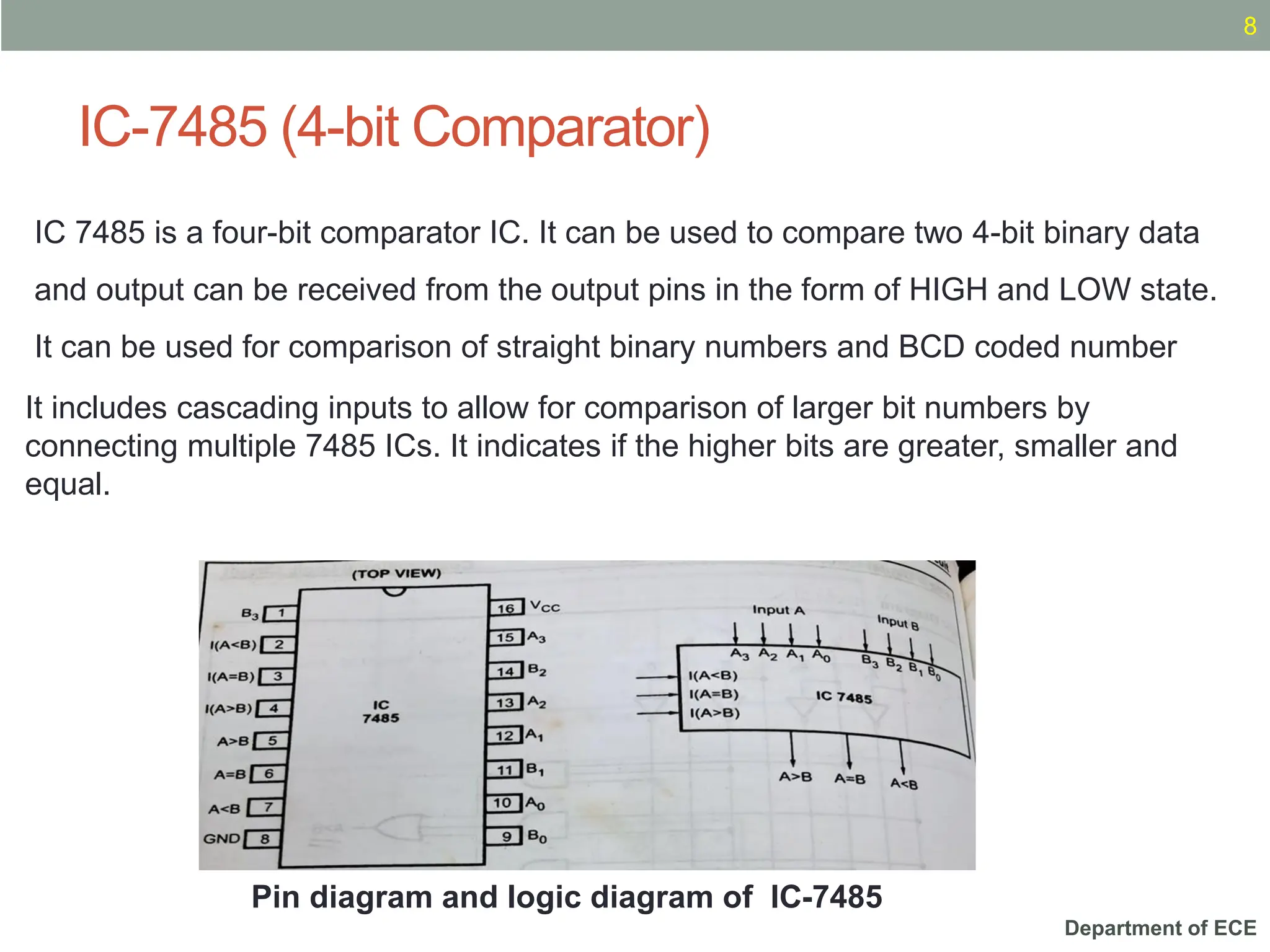
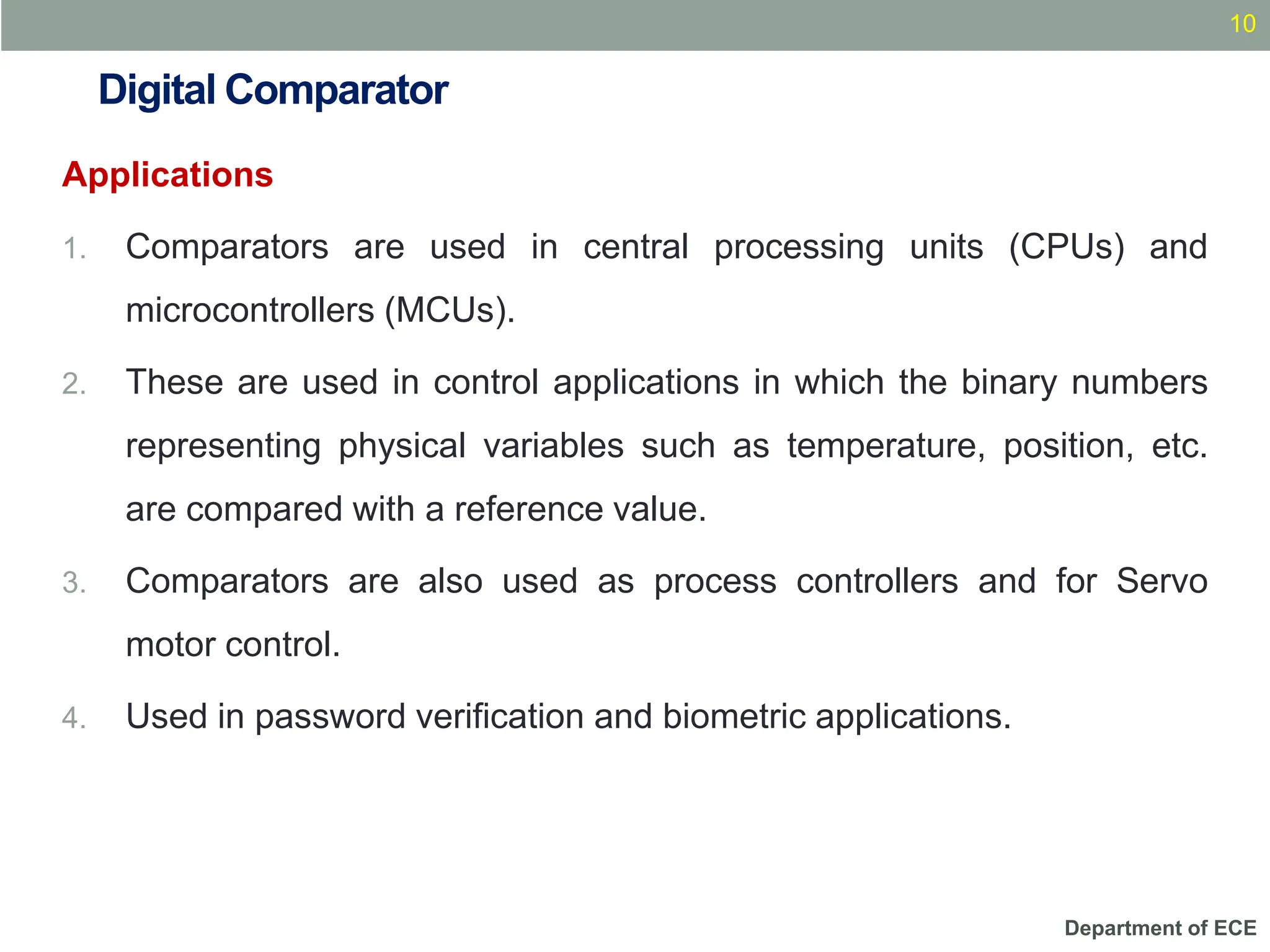
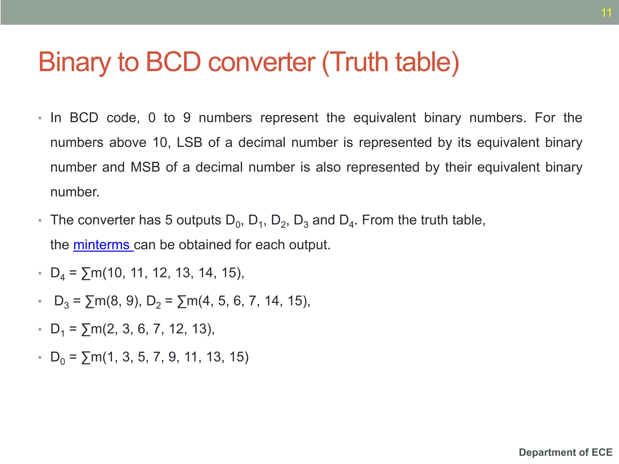
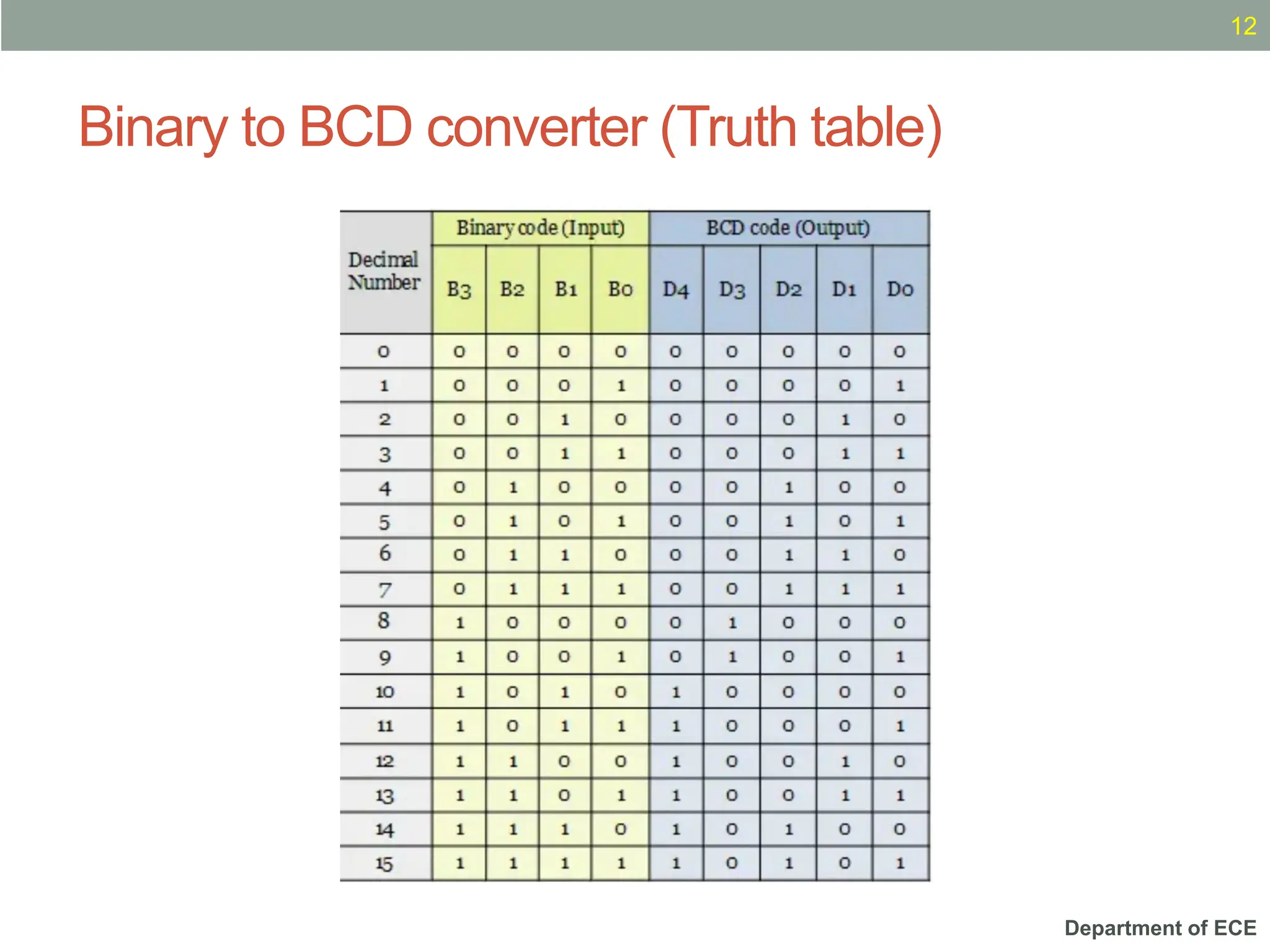
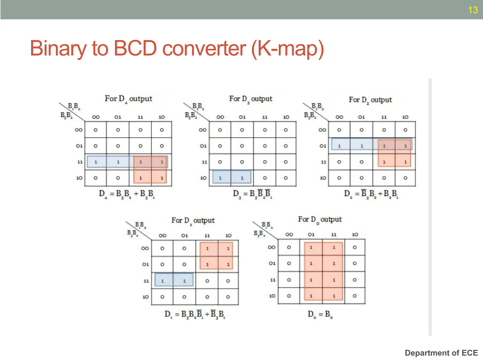
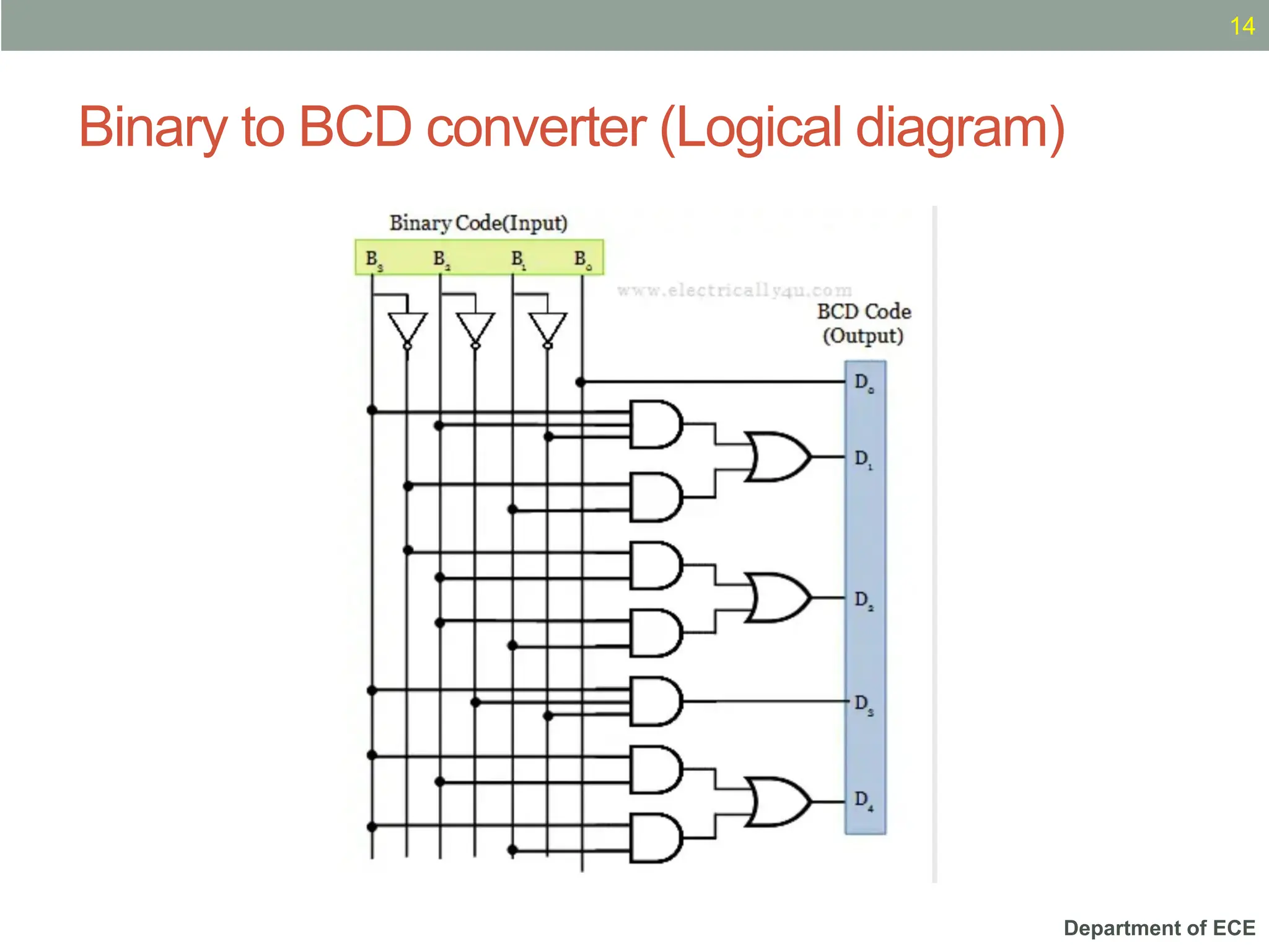
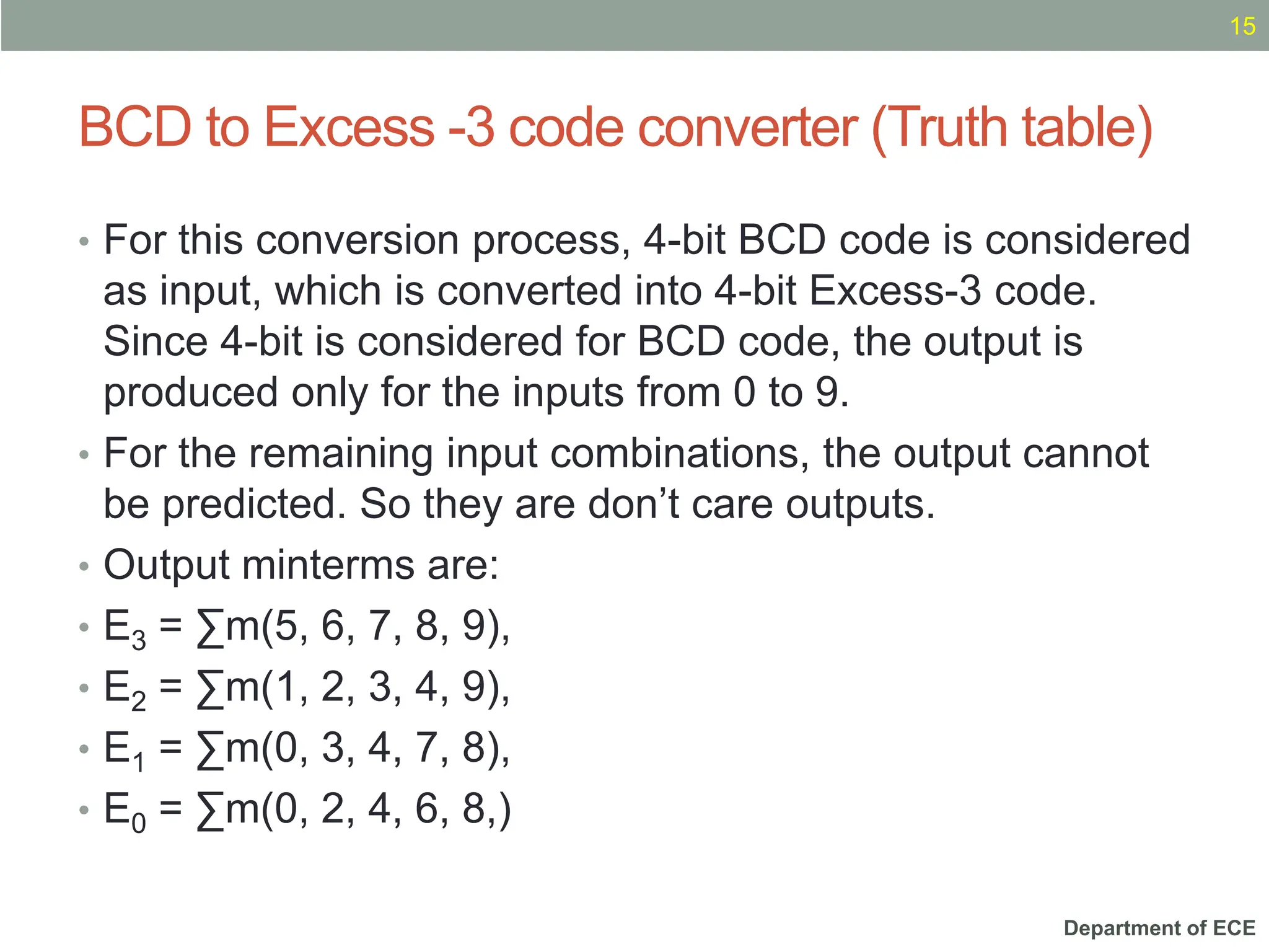
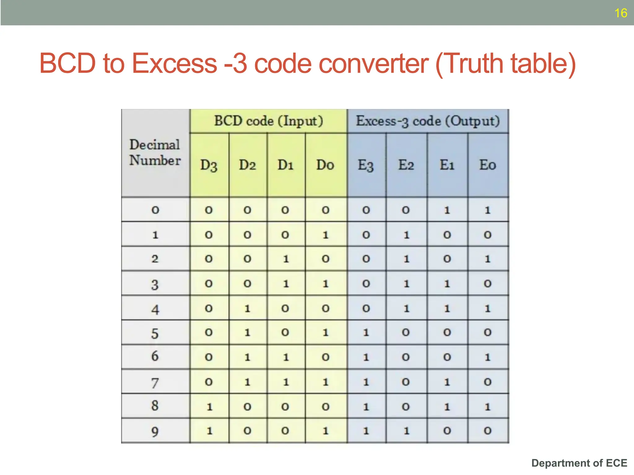
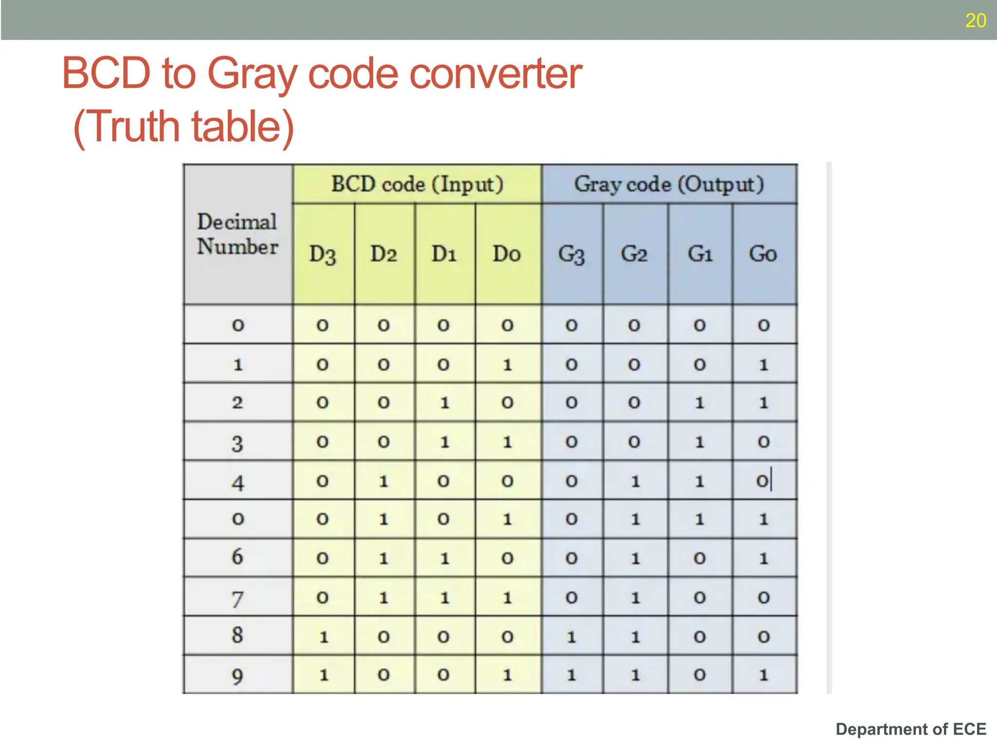
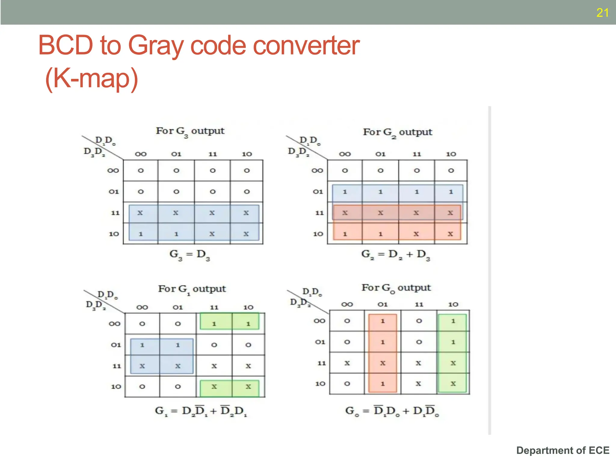
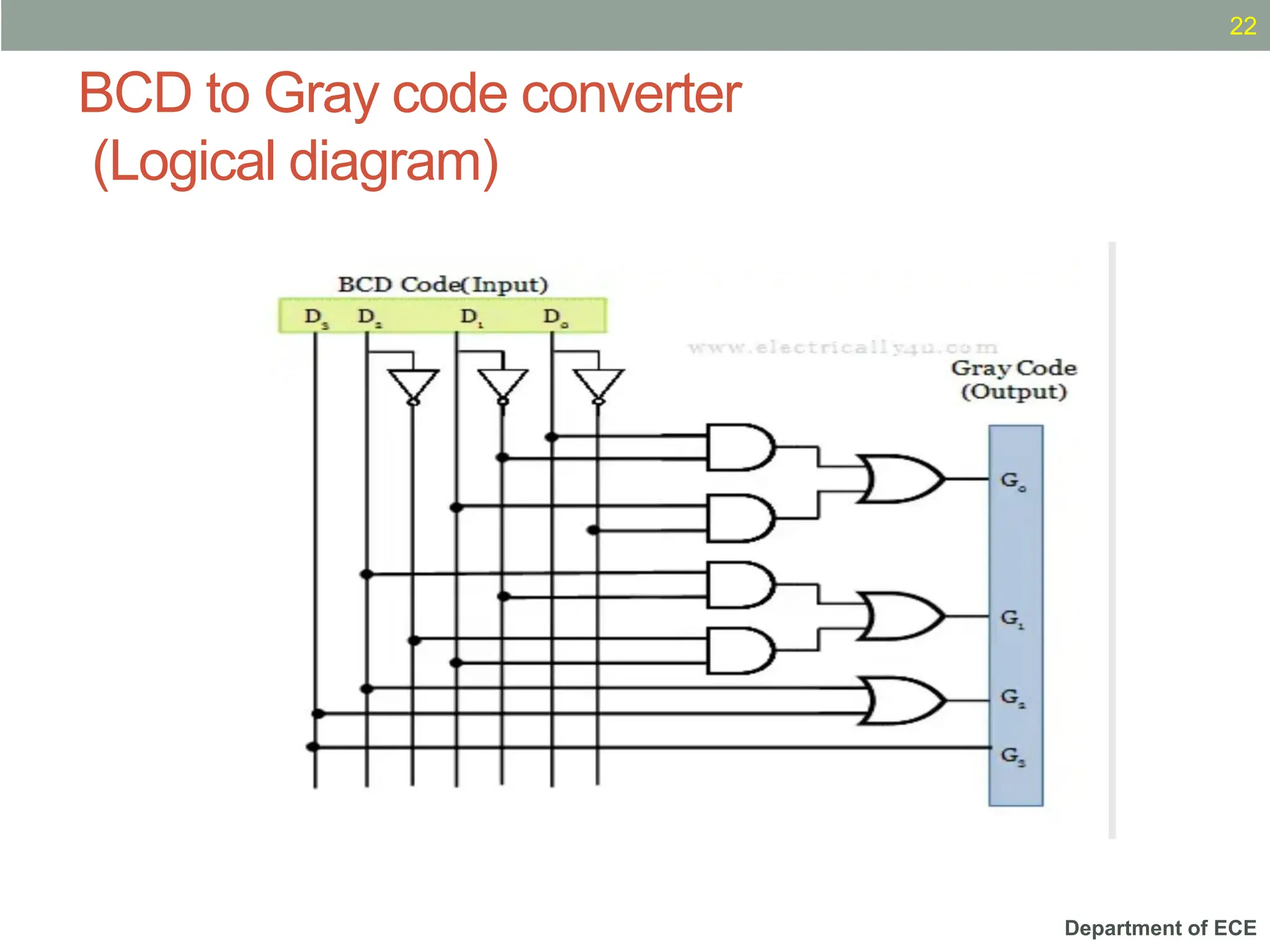
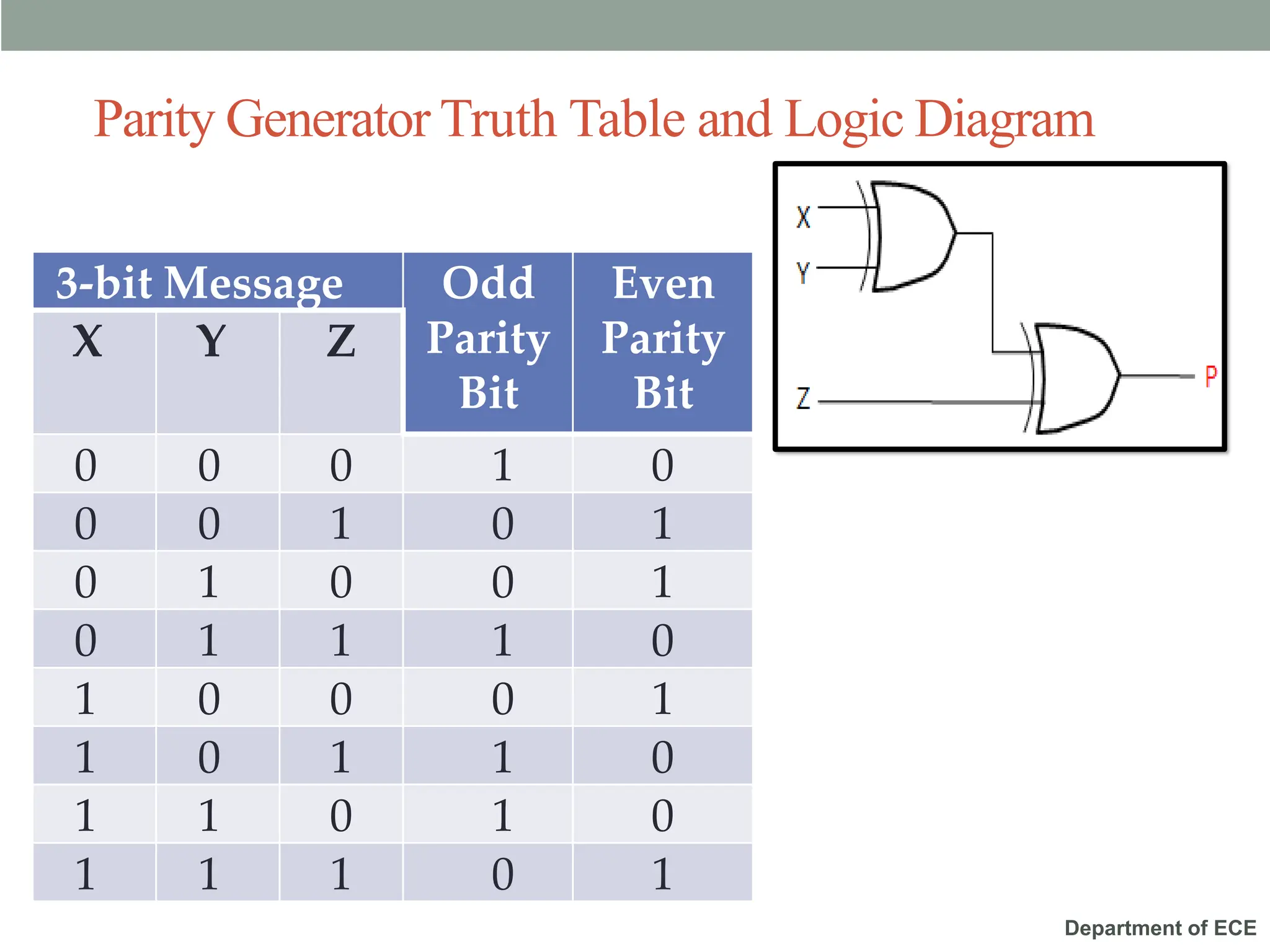
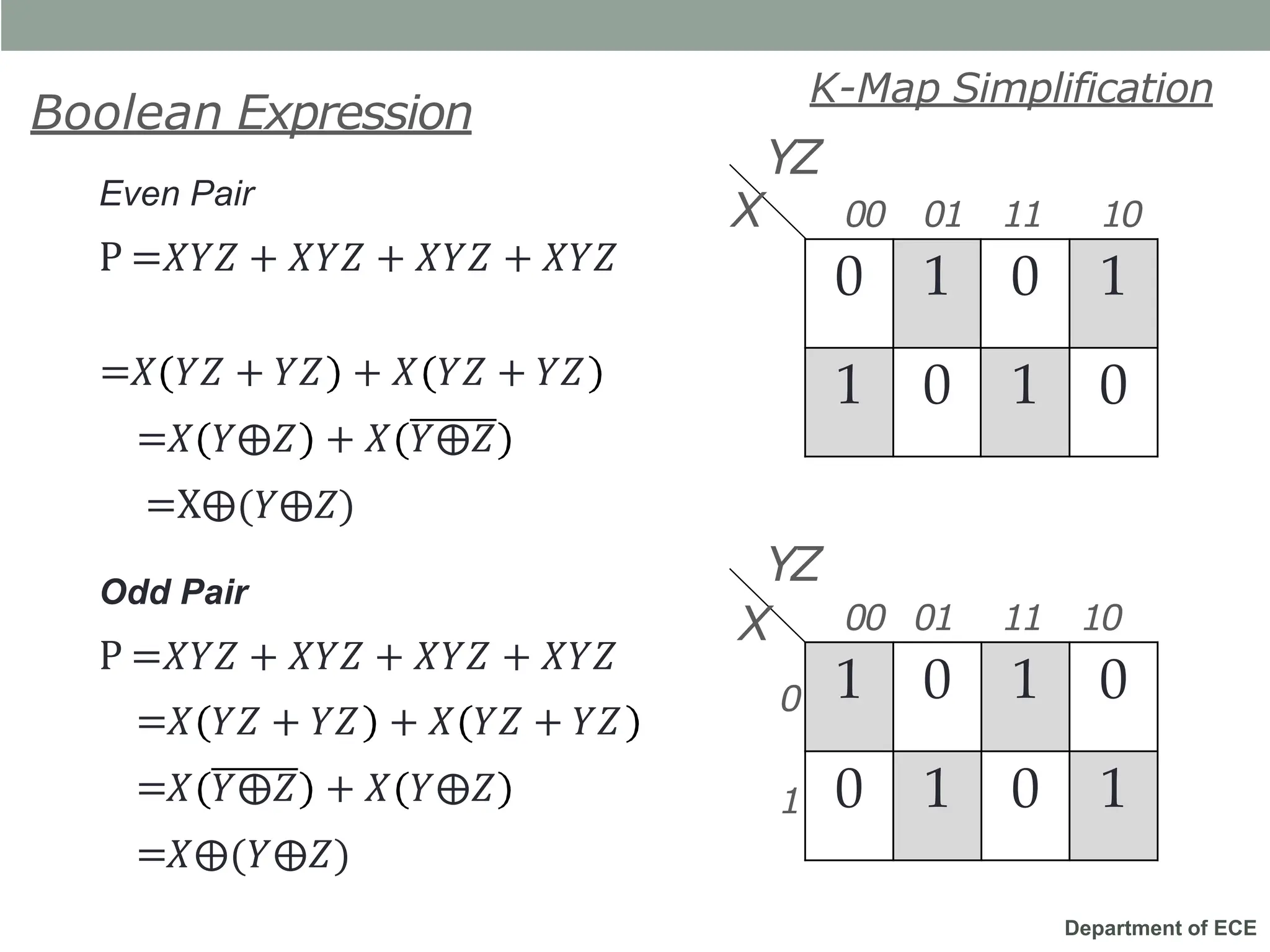
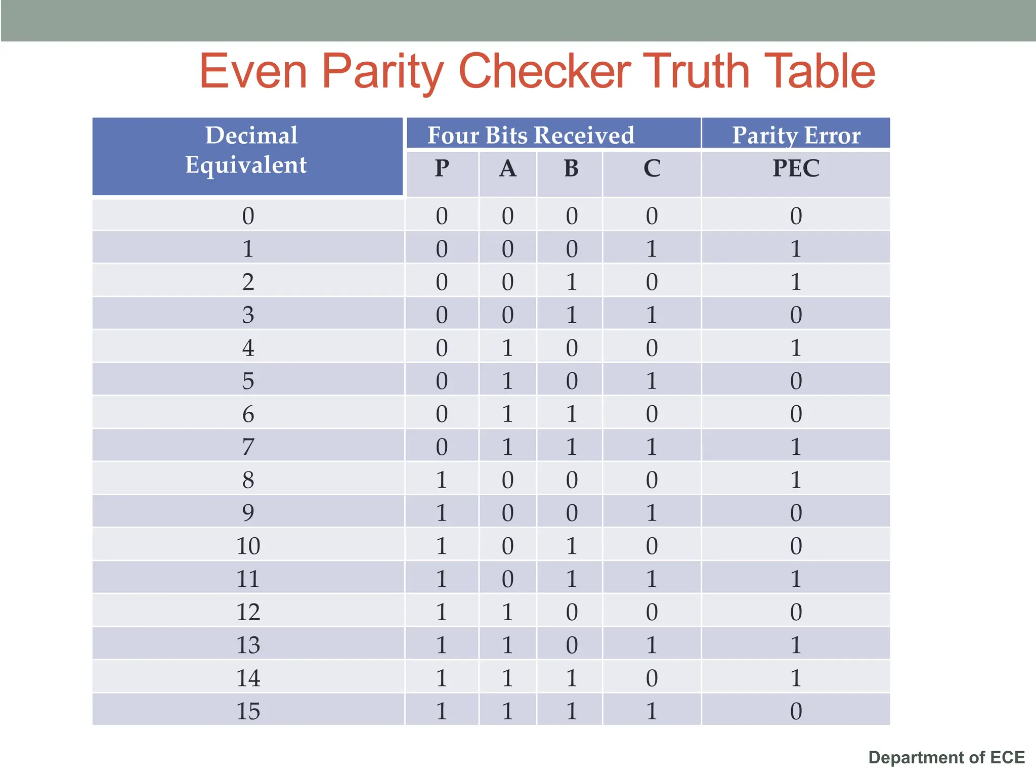
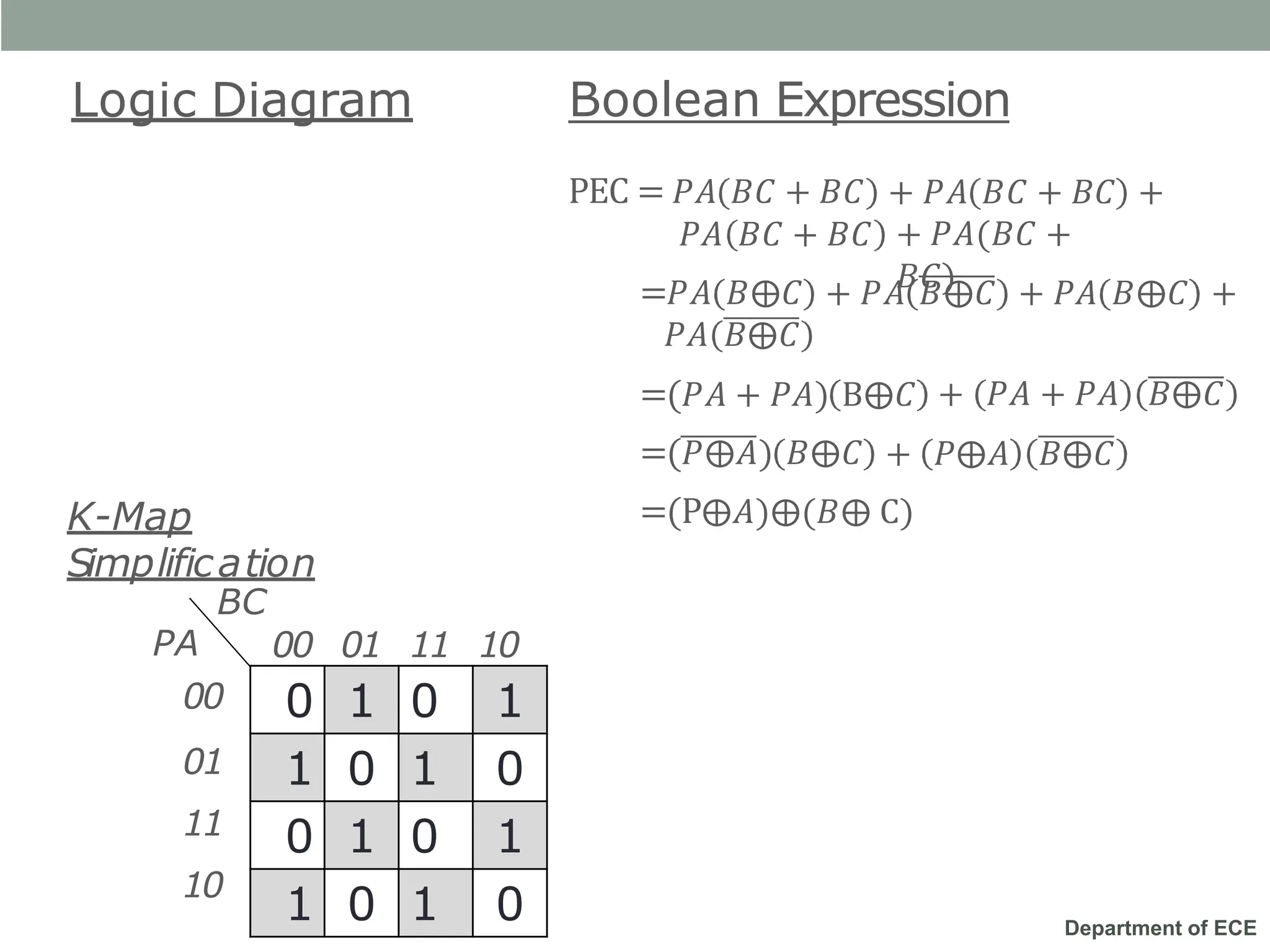
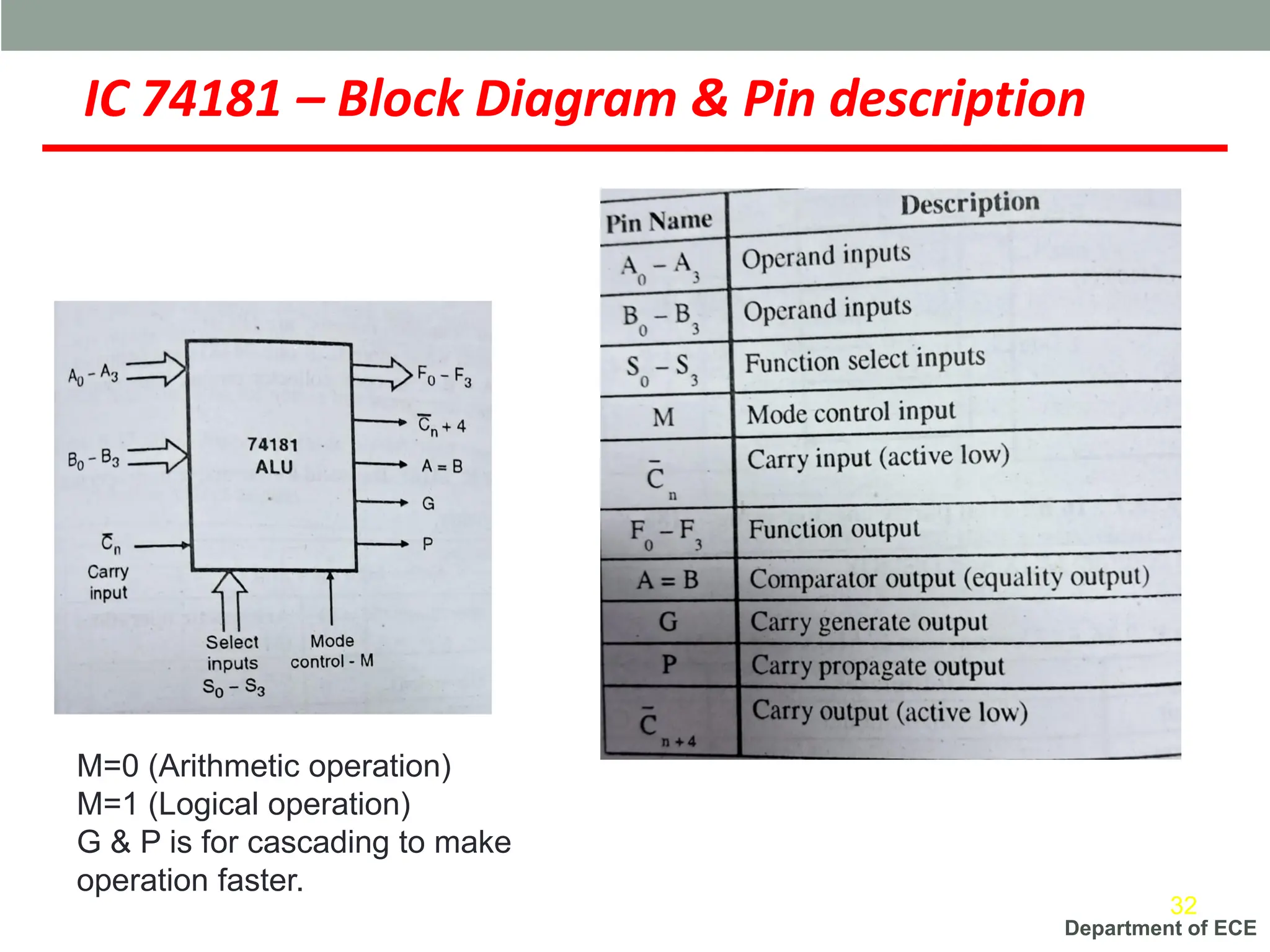
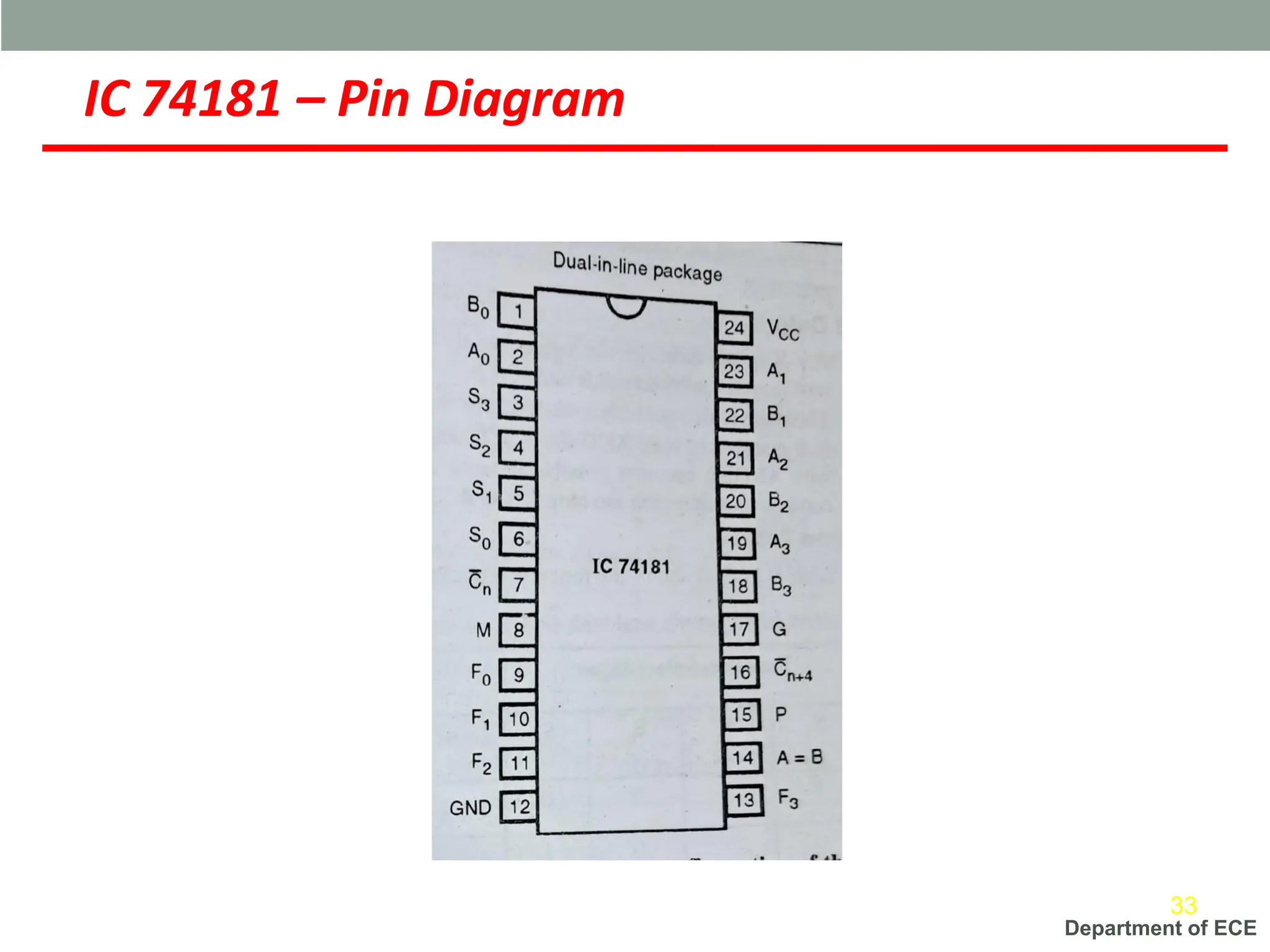
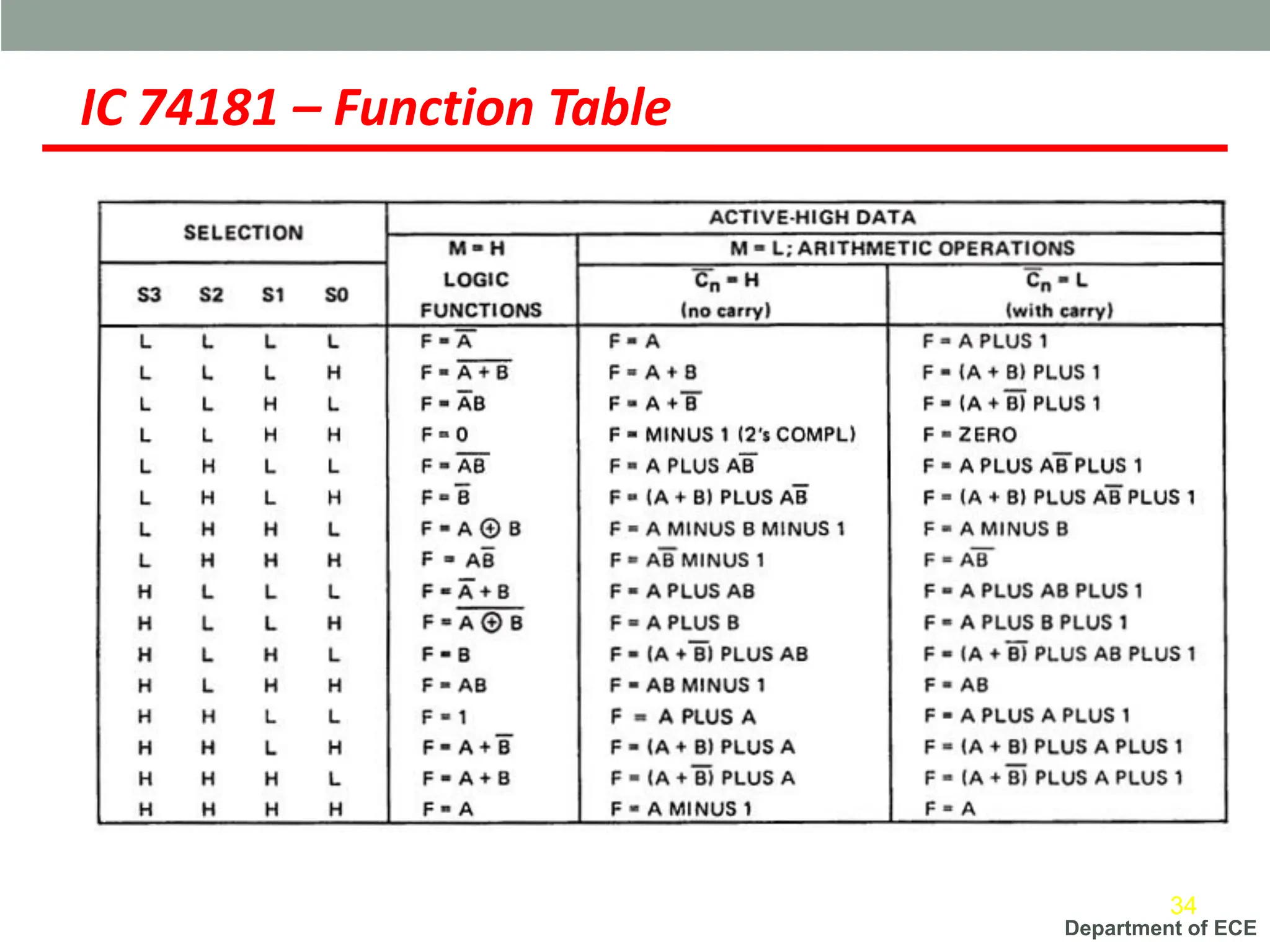
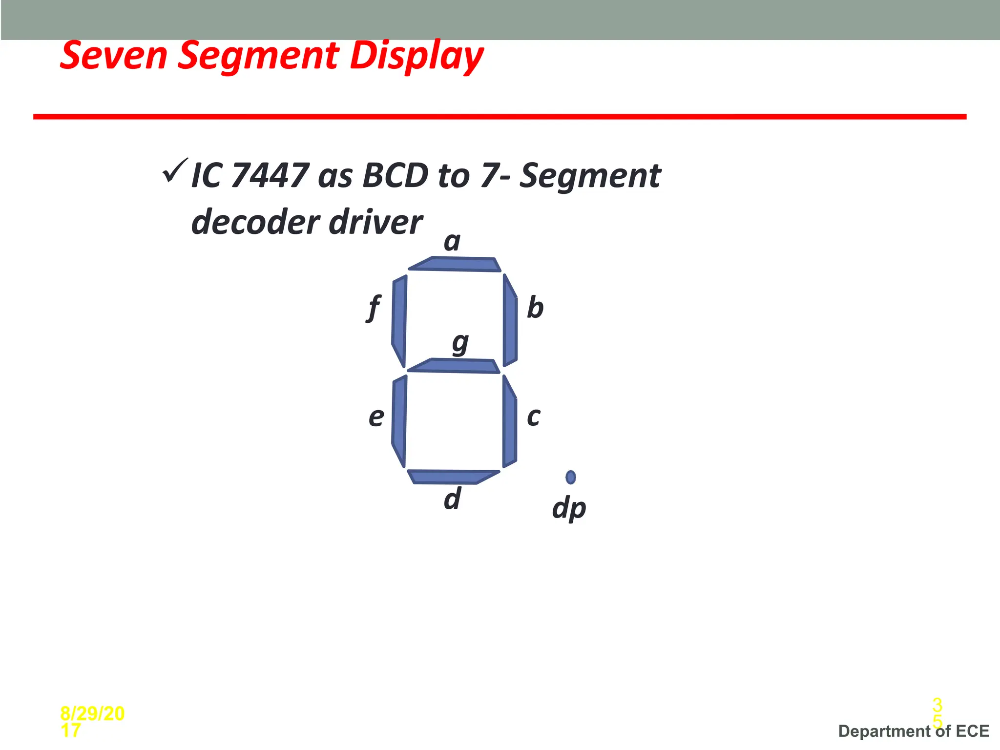
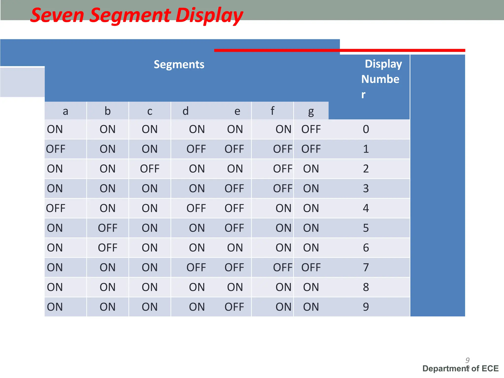
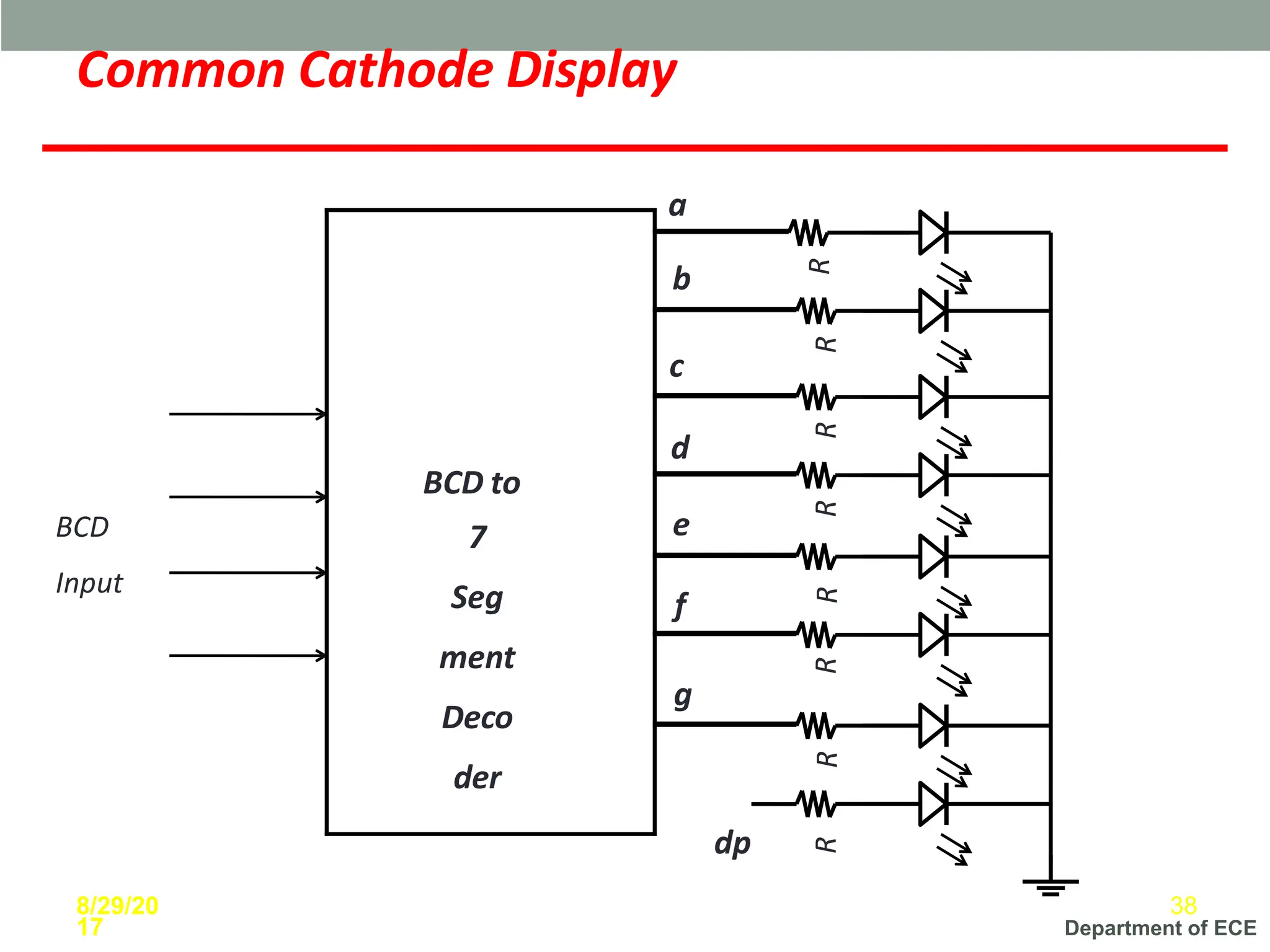
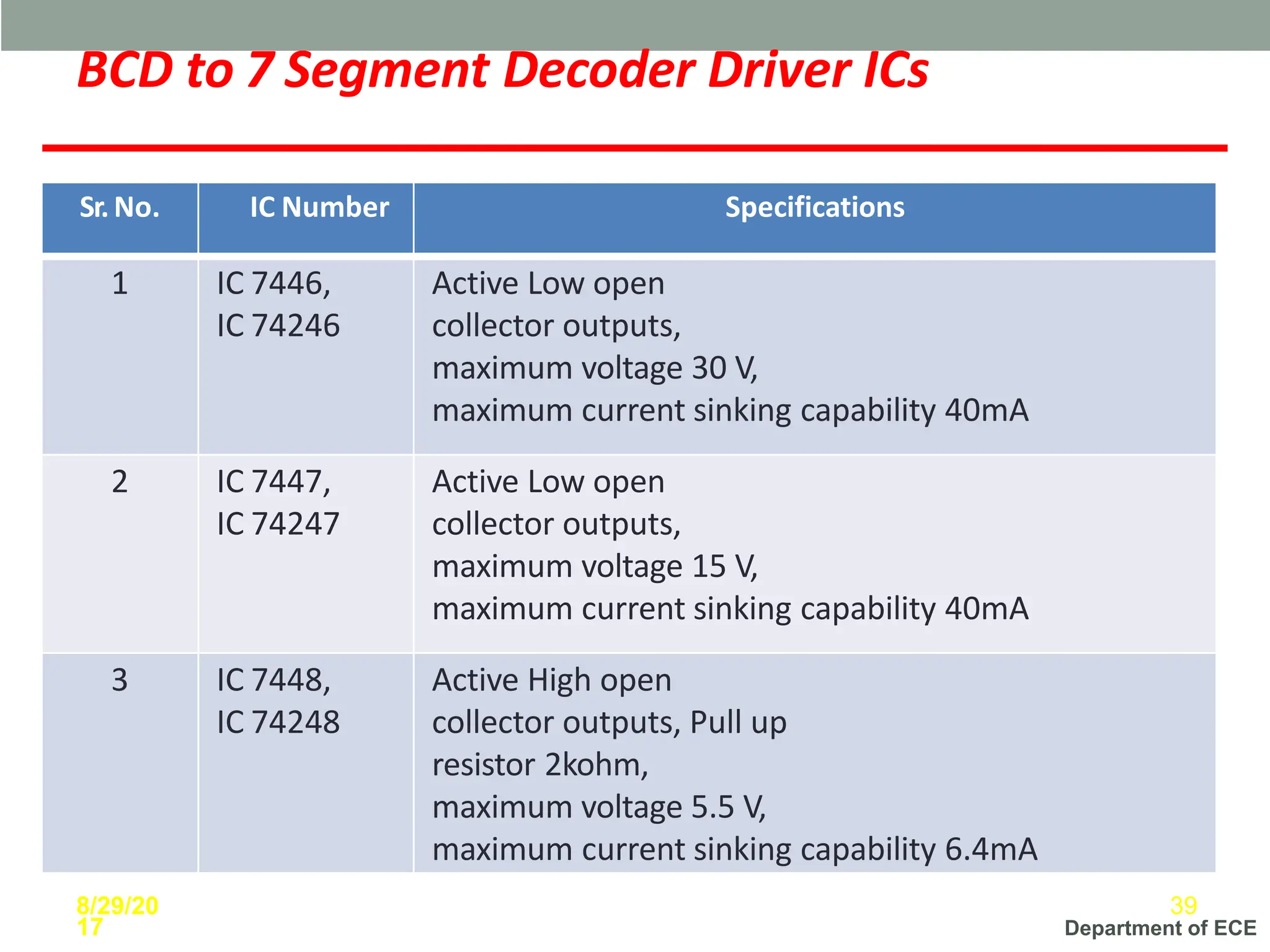
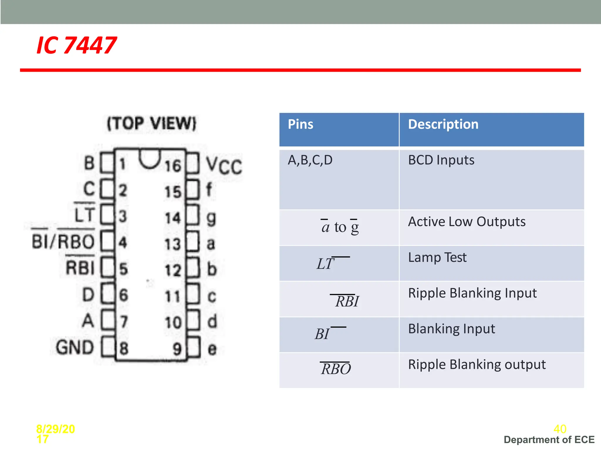
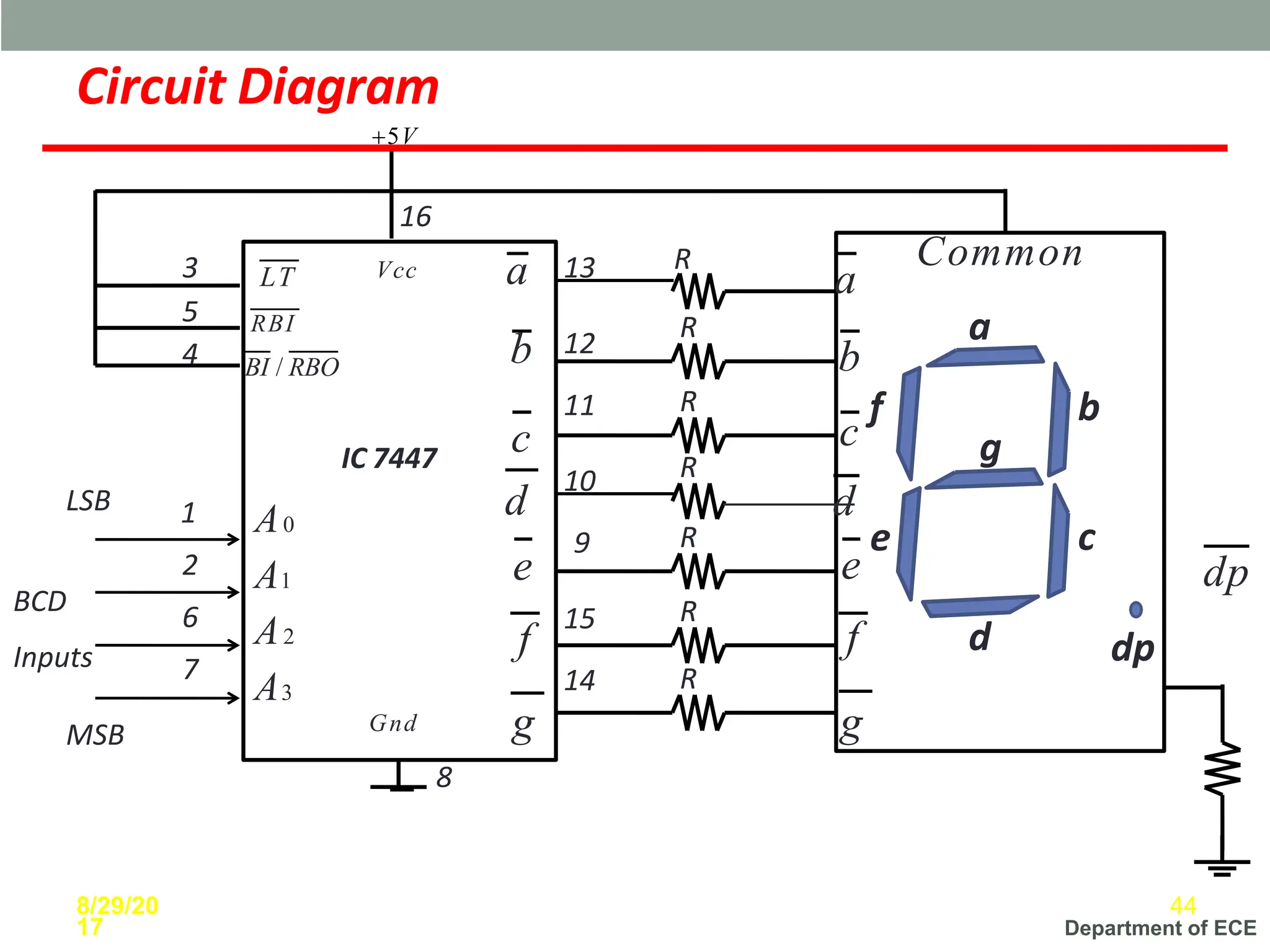
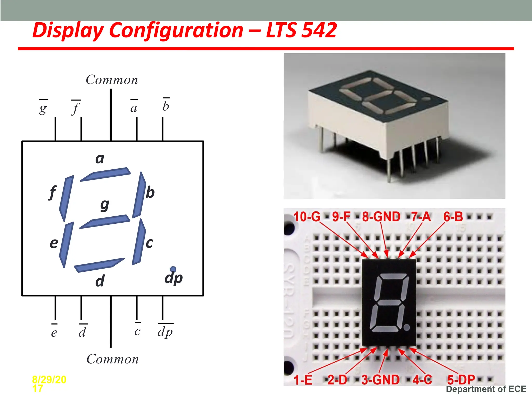
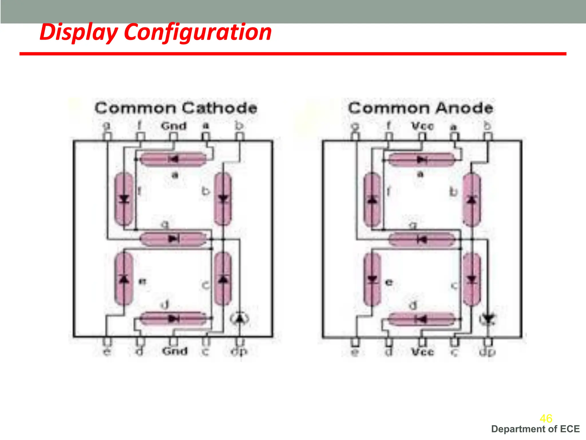
Department of ECE
INTRODUCTION OF COMBINATIONALCIRCUITS
A combinational circuit consists of input variables, logic gates, and
output variables. The output of combinational circuit at any instant,
depends only on the levels present at input terminals.
- It does not use any memory
- it can have number inputs and outputs.
Example:
1. Adder, Substractor
2. Comparator
3. Code Converters
4. Encoders, Decoders
5. Multiplexers and Demutiplexers
Department of ECE
Digital Comparator
▪ A magnitude digital Comparator is a combinational circuit that
compares two digital or binary numbers in order to find out
whether one binary number is equal, less than or greater than the
other binary number.
▪ We logically design a circuit for two inputs one for A and other for B
and have three output terminals, one for A > B condition, one for A = B
condition and one for A < B condition.
Module 2
Department of ECE
Digital Comparator
1-Bit Magnitude Comparator
▪ A comparator used to compare two bits is called a single bit comparator.
▪ It consists of two inputs each for two single bit numbers and three output.
▪ The truth table for a 1-bit comparator is given below:
▪ From the above truth table logical expressions for each output can be
expressed as follows:
A>B: AB'
A<B: A'B
A=B: A'B' + AB
3
Module 2
Department of ECE
Digital Comparator
▪ A comparator used to compare
two binary numbers each of two
bits is called a 2-bit Magnitude
comparator. It consists of four
inputs and three outputs to
generate less than, equal to and
greater than between two binary
numbers.
▪ The truth table for a 2-bit
comparator is given below:
4
Module 2
2-Bit Magnitude Comparator
Department of ECE
2-Bit Magnitude Comparator
From the above truth table K-map for each output can be drawn as follows:
5
Module 2
Department of ECE
2.2 Magnitude Comparator (K-map simplification)
2-Bit Magnitude Comparator
A>B: A1B1’ + A0B1’B0’ + A1A0B0’
A=B: A1’A0’B1’B0’ + A1’A0B1’B0 + A1A0B1B0 + A1A0’B1B0’
= A1’B1’ (A0’B0’ + A0B0) + A1B1 (A0B0 + A0’B0’)
= (A0B0 + A0’B0’) (A1B1 + A1’B1’)
= (A0 Ex-Nor B0) (A1 Ex-Nor B1)
A<B: A1’B1 + A0’B1B0 + A1’A0’B0
6
Module 2
22EC401 DIGITAL SYSTEM DESIGN
Department of ECE
Logic Diagram
2-Bit Magnitude Comparator
7
Module 2
Department of ECE
IC-7485 (4-bit Comparator)
8
Pin diagram and logic diagram of IC-7485
IC 7485 is a four-bit comparator IC. It can be used to compare two 4-bit binary data
and output can be received from the output pins in the form of HIGH and LOW state.
It can be used for comparison of straight binary numbers and BCD coded number
It includes cascading inputs to allow for comparison of larger bit numbers by
connecting multiple 7485 ICs. It indicates if the higher bits are greater, smaller and
equal.
Department of ECE
IC-7485 (4-bit Comparator)
9
Functional table for IC-7485
Comparing 8 bit number by cascading two 7485 IC’s-
Department of ECE
Digital Comparator
Applications
1. Comparators are used in central processing units (CPUs) and
microcontrollers (MCUs).
2. These are used in control applications in which the binary numbers
representing physical variables such as temperature, position, etc.
are compared with a reference value.
3. Comparators are also used as process controllers and for Servo
motor control.
4. Used in password verification and biometric applications.
10
Department of ECE
Binary to BCD converter (Truth table)
11
• In BCD code, 0 to 9 numbers represent the equivalent binary numbers. For the
numbers above 10, LSB of a decimal number is represented by its equivalent binary
number and MSB of a decimal number is also represented by their equivalent binary
number.
• The converter has 5 outputs D0, D1, D2, D3 and D4. From the truth table,
the minterms can be obtained for each output.
• D4 = ∑m(10, 11, 12, 13, 14, 15),
• D3 = ∑m(8, 9), D2 = ∑m(4, 5, 6, 7, 14, 15),
• D1 = ∑m(2, 3, 6, 7, 12, 13),
• D0 = ∑m(1, 3, 5, 7, 9, 11, 13, 15)
Department of ECE
Binary to BCD converter (Truth table)
12
Department of ECE
Binary to BCD converter (K-map)
13
Department of ECE
Binary to BCD converter (Logical diagram)
14
Department of ECE
BCD to Excess -3 code converter (Truth table)
15
• For this conversion process, 4-bit BCD code is considered
as input, which is converted into 4-bit Excess-3 code.
Since 4-bit is considered for BCD code, the output is
produced only for the inputs from 0 to 9.
• For the remaining input combinations, the output cannot
be predicted. So they are don’t care outputs.
• Output minterms are:
• E3 = ∑m(5, 6, 7, 8, 9),
• E2 = ∑m(1, 2, 3, 4, 9),
• E1 = ∑m(0, 3, 4, 7, 8),
• E0 = ∑m(0, 2, 4, 6, 8,)
Department of ECE
BCD to Excess -3 code converter (Truth table)
16
Department of ECE
BCD to Excess -3 code converter
(K-map)
17
Department of ECE
BCD to Excess -3 code converter
(Logical diagram)
18
Department of ECE
BCD to Gray code converter
(Truth table)
19
• The truth table having the conversion from BCD code to
gray code is shown below. Since the BCD code has only
4 bits, a total of 9 BCD digits have been considered. The
output is unpredictable for other input combinations.
Department of ECE
BCD to Gray code converter
(Truth table)
20
Department of ECE
BCD to Gray code converter
(K-map)
21
Department of ECE
BCD to Gray code converter
(Logical diagram)
22
Department of ECE
What is Parity Generator?
• AParity Generator is a Combinational Logic Circuit that
Generates the Parity bit in the Transmitter.
• AParity bit is used for the purpose of detecting errors during
transmissions of binary information.
• It is an extra bit included with the binary message to make
the number of 1’s either Odd or Even.
Department of ECE
Two Types of Parity
• In Even Parity, the added Parity bit will Make the Total
Number of 1’s an EvenAmount.
• In Odd Parity, the added Parity bit will Make the Total
Number of 1’s an OddAmount.
Department of ECE
Parity Generator Truth Table and Logic Diagram
3-bit Message Odd
Parity
Bit
Even
Parity
Bit
X Y Z
0 0 0 1 0
0 0 1 0 1
0 1 0 0 1
0 1 1 1 0
1 0 0 0 1
1 0 1 1 0
1 1 0 1 0
1 1 1 0 1
Department of ECE
Even Pair
P =𝑋𝑌𝑍 + 𝑋𝑌𝑍 + 𝑋𝑌𝑍 + 𝑋𝑌𝑍
+ 𝑋 𝑌𝑍 + 𝑌𝑍
=𝑋 𝑌𝑍 + 𝑌𝑍
=𝑋 𝑌⨁𝑍 + 𝑋 𝑌⨁𝑍
0 1 0 1
1 0 1 0
YZ
X 00 01 11 10
0
1
Boolean Expression
K-Map Simplification
=X⨁(𝑌⨁𝑍)
Odd Pair
P =𝑋𝑌𝑍 + 𝑋𝑌𝑍 + 𝑋𝑌𝑍 + 𝑋𝑌𝑍
=𝑋 𝑌𝑍 + 𝑌𝑍 + 𝑋 𝑌𝑍 + 𝑌𝑍
=𝑋 𝑌⨁𝑍 + 𝑋 𝑌⨁𝑍
=𝑋⨁(𝑌⨁𝑍)
1 0 1 0
0 1 0 1
X
YZ
00 01 11 10
Department of ECE
Parity Checker
• ACircuit that Checks the Parity in the Receiver is called
Parity Checker.
• The Parity Checker circuit checks for possible errors in the
Transmission.
• Since the Information Transmitted with Even Parity, the
Receiver must have an even number of 1’s.If it has odd
number of 1’s, it indicates that there is an error occurred
during Transmission.
• The Output of the Parity Checker is denoted by PEC(Parity
Error Checker).If there is error, that is,if it has odd number of
1’s, it will indicate 1.If no then PEC will indicate 0.
Department of ECE
Decimal
Equivalent
Four Bits Received Parity Error
P A B C PEC
0 0 0 0 0 0
1 0 0 0 1 1
2 0 0 1 0 1
3 0 0 1 1 0
4 0 1 0 0 1
5 0 1 0 1 0
6 0 1 1 0 0
7 0 1 1 1 1
8 1 0 0 0 1
9 1 0 0 1 0
10 1 0 1 0 0
11 1 0 1 1 1
12 1 1 0 0 0
13 1 1 0 1 1
14 1 1 1 0 1
15 1 1 1 1 0
Even Parity Checker Truth Table
Department of ECE
Logic Diagram Boolean Expression
+ 𝑃𝐴 𝐵𝐶 + 𝐵𝐶 +
PEC = 𝑃𝐴 𝐵𝐶 + 𝐵𝐶
𝑃𝐴 𝐵𝐶 + 𝐵𝐶 + 𝑃𝐴(𝐵𝐶 +
𝐵𝐶)
=𝑃𝐴 𝐵⨁𝐶 + 𝑃𝐴 𝐵⨁𝐶 + 𝑃𝐴 𝐵⨁𝐶 +
𝑃𝐴 𝐵⨁𝐶
=(𝑃𝐴 + 𝑃𝐴) B⨁𝐶
=(𝑃⨁𝐴) 𝐵⨁𝐶
+ 𝑃𝐴 + 𝑃𝐴 𝐵⨁𝐶
+ 𝑃⨁𝐴 𝐵⨁𝐶
=(P⨁𝐴)⨁(𝐵⨁ C)
0 1 0 1
1 0 1 0
0 1 0 1
1 0 1 0
00 01 11 10
00
01
11
10
PA
K-Map
Simplification
BC
Department of ECE
IC 74181 – Arithmetic Logic Unit
➢A very popular & widely used combinational
circuit is ALU which is capable of performing
arithmetic as well as logical operation.
➢Arithmetic Operating Modes:
✓Addition
✓Subtraction
✓Shift Operation
✓Magnitude Comparison
✓12 other arithmetic operations
8/29/20
17
30
Department of ECE
IC 74381 – 4 Bit Arithmetic Logic Unit
➢Features:
✓Low input loading minimizes drive requirements
✓Performs sixteen arithmetic and 16 logical
functions
✓Carry generate and propagate outputs for use
with carry look ahead generator
31
Department of ECE
IC 74181 – Block Diagram & Pin description
32
M=0 (Arithmetic operation)
M=1 (Logical operation)
G & P is for cascading to make
operation faster.
Department of ECE
IC 74181 – Pin Diagram
33
Department of ECE
IC 74181 – Function Table
34
Department of ECE
Seven Segment Display
a
b
c
d
e
f
g
dp
8/29/20
17
3
5
✓IC 7447 as BCD to 7- Segment
decoder driver
Department of ECE
Seven Segment Display
9
9
Segments Display
Numbe
r
a b c d e f g
ON ON ON ON ON ON OFF 0
OFF ON ON OFF OFF OFF OFF 1
ON ON OFF ON ON OFF ON 2
ON ON ON ON OFF OFF ON 3
OFF ON ON OFF OFF ON ON 4
ON OFF ON ON OFF ON ON 5
ON OFF ON ON ON ON ON 6
ON ON ON OFF OFF OFF OFF 7
ON ON ON ON ON ON ON 8
ON ON ON ON OFF ON ON 9
Department of ECE
Types of Seven Segment Display
➢Common Cathode Display
➢Common Anode Display
8/29/20
17
37
Department of ECE
Common Cathode Display
BCD
Input
R
8/29/20
17
38
R
R
R
R
R
R
R
a
BCD to
7
Seg
ment
Deco
der
b
c
d
e
f
g
dp
Department of ECE
BCD to 7 Segment Decoder Driver ICs
Sr.No. IC Number Specifications
1 IC 7446,
IC 74246
Active Low open
collector outputs,
maximum voltage 30 V,
maximum current sinking capability 40mA
2 IC 7447,
IC 74247
Active Low open
collector outputs,
maximum voltage 15 V,
maximum current sinking capability 40mA
3 IC 7448,
IC 74248
Active High open
collector outputs, Pull up
resistor 2kohm,
maximum voltage 5.5 V,
maximum current sinking capability 6.4mA
8/29/20
17
39
Department of ECE
IC 7447
Pins Description
A,B,C,D BCD Inputs
a to g Active Low Outputs
LT Lamp Test
RBI
Ripple Blanking Input
BI Blanking Input
RBO Ripple Blanking output
8/29/20
17
40
Department of ECE
– Blanking Input
✓If BI is connected to 0, then the display will be
switched off irrespective of the BCD input.
✓This feature is used in the multiplexed display
in order to save power.
✓In the non-multiplexed displays this input is
permanently connected to Vcc(1)
BI/RBO
41
Department of ECE
✓This pin can be used to check whether all the
segments of the display are working properly
or not.
✓If LT is forced low with RBO at logic 1 or open ,
then all the output terminals will be forced to
their active state.
LT - Lamp Test
8/29/20
17
42
Department of ECE
- Ripple Blanking Input
✓For the normal decoding operation, this input
should be connected to logic 1.
✓If RBI is connected to ground, then it switches
off the display when BCD inputs
corresponding to 0.(0 0 0 0)
✓For non-zero BCD inputs, the decoder output
will be normal and the BCD number will be
displayed.
✓RBI=0 is connected for blanking out the
RBI
107
leading zeros in multidigit displays.
Department of ECE
a
b
c
d
e
g
dp
R
R
R
R
R
R
1
2
6
7
3
5
4
13 R
12
11
10
9
15
16
14
8
BCD
Inputs
LSB
MSB
IC 7447
a
b
c
d
e
f
g
dp
LT
RBI
BI / RBO
Vcc
Gnd
A0
A1
A2
A3
Circuit Diagram
+5V
a
b
c
f
d
e
f
g
8/29/20
17
44
Common
Department of ECE
Display Configuration – LTS 542
11
2
a
b
c
d
e
f
g
dp
a b
c
e d
f
g
dp
8/29/20
17
Common
Common
Department of ECE
Display Configuration
46
Department of ECE
References
✓Digital Principles by
Malvino Leach
✓Modern Digital
Electronics by R.P. Jain
✓Digital Electronics,
Principles and Integrated
Circuits by Anil K. Maini
✓Digital Techniques by A.
Anand Kumar
47

Analogue & Digital Electronics on Comparators

  • 1.
    Department of ECE INTRODUCTIONOF COMBINATIONALCIRCUITS A combinational circuit consists of input variables, logic gates, and output variables. The output of combinational circuit at any instant, depends only on the levels present at input terminals. - It does not use any memory - it can have number inputs and outputs. Example: 1. Adder, Substractor 2. Comparator 3. Code Converters 4. Encoders, Decoders 5. Multiplexers and Demutiplexers
  • 2.
    Department of ECE DigitalComparator ▪ A magnitude digital Comparator is a combinational circuit that compares two digital or binary numbers in order to find out whether one binary number is equal, less than or greater than the other binary number. ▪ We logically design a circuit for two inputs one for A and other for B and have three output terminals, one for A > B condition, one for A = B condition and one for A < B condition. Module 2
  • 3.
    Department of ECE DigitalComparator 1-Bit Magnitude Comparator ▪ A comparator used to compare two bits is called a single bit comparator. ▪ It consists of two inputs each for two single bit numbers and three output. ▪ The truth table for a 1-bit comparator is given below: ▪ From the above truth table logical expressions for each output can be expressed as follows: A>B: AB' A<B: A'B A=B: A'B' + AB 3 Module 2
  • 4.
    Department of ECE DigitalComparator ▪ A comparator used to compare two binary numbers each of two bits is called a 2-bit Magnitude comparator. It consists of four inputs and three outputs to generate less than, equal to and greater than between two binary numbers. ▪ The truth table for a 2-bit comparator is given below: 4 Module 2 2-Bit Magnitude Comparator
  • 5.
    Department of ECE 2-BitMagnitude Comparator From the above truth table K-map for each output can be drawn as follows: 5 Module 2
  • 6.
    Department of ECE 2.2Magnitude Comparator (K-map simplification) 2-Bit Magnitude Comparator A>B: A1B1’ + A0B1’B0’ + A1A0B0’ A=B: A1’A0’B1’B0’ + A1’A0B1’B0 + A1A0B1B0 + A1A0’B1B0’ = A1’B1’ (A0’B0’ + A0B0) + A1B1 (A0B0 + A0’B0’) = (A0B0 + A0’B0’) (A1B1 + A1’B1’) = (A0 Ex-Nor B0) (A1 Ex-Nor B1) A<B: A1’B1 + A0’B1B0 + A1’A0’B0 6 Module 2 22EC401 DIGITAL SYSTEM DESIGN
  • 7.
    Department of ECE LogicDiagram 2-Bit Magnitude Comparator 7 Module 2
  • 8.
    Department of ECE IC-7485(4-bit Comparator) 8 Pin diagram and logic diagram of IC-7485 IC 7485 is a four-bit comparator IC. It can be used to compare two 4-bit binary data and output can be received from the output pins in the form of HIGH and LOW state. It can be used for comparison of straight binary numbers and BCD coded number It includes cascading inputs to allow for comparison of larger bit numbers by connecting multiple 7485 ICs. It indicates if the higher bits are greater, smaller and equal.
  • 9.
    Department of ECE IC-7485(4-bit Comparator) 9 Functional table for IC-7485 Comparing 8 bit number by cascading two 7485 IC’s-
  • 10.
    Department of ECE DigitalComparator Applications 1. Comparators are used in central processing units (CPUs) and microcontrollers (MCUs). 2. These are used in control applications in which the binary numbers representing physical variables such as temperature, position, etc. are compared with a reference value. 3. Comparators are also used as process controllers and for Servo motor control. 4. Used in password verification and biometric applications. 10
  • 11.
    Department of ECE Binaryto BCD converter (Truth table) 11 • In BCD code, 0 to 9 numbers represent the equivalent binary numbers. For the numbers above 10, LSB of a decimal number is represented by its equivalent binary number and MSB of a decimal number is also represented by their equivalent binary number. • The converter has 5 outputs D0, D1, D2, D3 and D4. From the truth table, the minterms can be obtained for each output. • D4 = ∑m(10, 11, 12, 13, 14, 15), • D3 = ∑m(8, 9), D2 = ∑m(4, 5, 6, 7, 14, 15), • D1 = ∑m(2, 3, 6, 7, 12, 13), • D0 = ∑m(1, 3, 5, 7, 9, 11, 13, 15)
  • 12.
    Department of ECE Binaryto BCD converter (Truth table) 12
  • 13.
    Department of ECE Binaryto BCD converter (K-map) 13
  • 14.
    Department of ECE Binaryto BCD converter (Logical diagram) 14
  • 15.
    Department of ECE BCDto Excess -3 code converter (Truth table) 15 • For this conversion process, 4-bit BCD code is considered as input, which is converted into 4-bit Excess-3 code. Since 4-bit is considered for BCD code, the output is produced only for the inputs from 0 to 9. • For the remaining input combinations, the output cannot be predicted. So they are don’t care outputs. • Output minterms are: • E3 = ∑m(5, 6, 7, 8, 9), • E2 = ∑m(1, 2, 3, 4, 9), • E1 = ∑m(0, 3, 4, 7, 8), • E0 = ∑m(0, 2, 4, 6, 8,)
  • 16.
    Department of ECE BCDto Excess -3 code converter (Truth table) 16
  • 17.
    Department of ECE BCDto Excess -3 code converter (K-map) 17
  • 18.
    Department of ECE BCDto Excess -3 code converter (Logical diagram) 18
  • 19.
    Department of ECE BCDto Gray code converter (Truth table) 19 • The truth table having the conversion from BCD code to gray code is shown below. Since the BCD code has only 4 bits, a total of 9 BCD digits have been considered. The output is unpredictable for other input combinations.
  • 20.
    Department of ECE BCDto Gray code converter (Truth table) 20
  • 21.
    Department of ECE BCDto Gray code converter (K-map) 21
  • 22.
    Department of ECE BCDto Gray code converter (Logical diagram) 22
  • 23.
    Department of ECE Whatis Parity Generator? • AParity Generator is a Combinational Logic Circuit that Generates the Parity bit in the Transmitter. • AParity bit is used for the purpose of detecting errors during transmissions of binary information. • It is an extra bit included with the binary message to make the number of 1’s either Odd or Even.
  • 24.
    Department of ECE TwoTypes of Parity • In Even Parity, the added Parity bit will Make the Total Number of 1’s an EvenAmount. • In Odd Parity, the added Parity bit will Make the Total Number of 1’s an OddAmount.
  • 25.
    Department of ECE ParityGenerator Truth Table and Logic Diagram 3-bit Message Odd Parity Bit Even Parity Bit X Y Z 0 0 0 1 0 0 0 1 0 1 0 1 0 0 1 0 1 1 1 0 1 0 0 0 1 1 0 1 1 0 1 1 0 1 0 1 1 1 0 1
  • 26.
    Department of ECE EvenPair P =𝑋𝑌𝑍 + 𝑋𝑌𝑍 + 𝑋𝑌𝑍 + 𝑋𝑌𝑍 + 𝑋 𝑌𝑍 + 𝑌𝑍 =𝑋 𝑌𝑍 + 𝑌𝑍 =𝑋 𝑌⨁𝑍 + 𝑋 𝑌⨁𝑍 0 1 0 1 1 0 1 0 YZ X 00 01 11 10 0 1 Boolean Expression K-Map Simplification =X⨁(𝑌⨁𝑍) Odd Pair P =𝑋𝑌𝑍 + 𝑋𝑌𝑍 + 𝑋𝑌𝑍 + 𝑋𝑌𝑍 =𝑋 𝑌𝑍 + 𝑌𝑍 + 𝑋 𝑌𝑍 + 𝑌𝑍 =𝑋 𝑌⨁𝑍 + 𝑋 𝑌⨁𝑍 =𝑋⨁(𝑌⨁𝑍) 1 0 1 0 0 1 0 1 X YZ 00 01 11 10
  • 27.
    Department of ECE ParityChecker • ACircuit that Checks the Parity in the Receiver is called Parity Checker. • The Parity Checker circuit checks for possible errors in the Transmission. • Since the Information Transmitted with Even Parity, the Receiver must have an even number of 1’s.If it has odd number of 1’s, it indicates that there is an error occurred during Transmission. • The Output of the Parity Checker is denoted by PEC(Parity Error Checker).If there is error, that is,if it has odd number of 1’s, it will indicate 1.If no then PEC will indicate 0.
  • 28.
    Department of ECE Decimal Equivalent FourBits Received Parity Error P A B C PEC 0 0 0 0 0 0 1 0 0 0 1 1 2 0 0 1 0 1 3 0 0 1 1 0 4 0 1 0 0 1 5 0 1 0 1 0 6 0 1 1 0 0 7 0 1 1 1 1 8 1 0 0 0 1 9 1 0 0 1 0 10 1 0 1 0 0 11 1 0 1 1 1 12 1 1 0 0 0 13 1 1 0 1 1 14 1 1 1 0 1 15 1 1 1 1 0 Even Parity Checker Truth Table
  • 29.
    Department of ECE LogicDiagram Boolean Expression + 𝑃𝐴 𝐵𝐶 + 𝐵𝐶 + PEC = 𝑃𝐴 𝐵𝐶 + 𝐵𝐶 𝑃𝐴 𝐵𝐶 + 𝐵𝐶 + 𝑃𝐴(𝐵𝐶 + 𝐵𝐶) =𝑃𝐴 𝐵⨁𝐶 + 𝑃𝐴 𝐵⨁𝐶 + 𝑃𝐴 𝐵⨁𝐶 + 𝑃𝐴 𝐵⨁𝐶 =(𝑃𝐴 + 𝑃𝐴) B⨁𝐶 =(𝑃⨁𝐴) 𝐵⨁𝐶 + 𝑃𝐴 + 𝑃𝐴 𝐵⨁𝐶 + 𝑃⨁𝐴 𝐵⨁𝐶 =(P⨁𝐴)⨁(𝐵⨁ C) 0 1 0 1 1 0 1 0 0 1 0 1 1 0 1 0 00 01 11 10 00 01 11 10 PA K-Map Simplification BC
  • 30.
    Department of ECE IC74181 – Arithmetic Logic Unit ➢A very popular & widely used combinational circuit is ALU which is capable of performing arithmetic as well as logical operation. ➢Arithmetic Operating Modes: ✓Addition ✓Subtraction ✓Shift Operation ✓Magnitude Comparison ✓12 other arithmetic operations 8/29/20 17 30
  • 31.
    Department of ECE IC74381 – 4 Bit Arithmetic Logic Unit ➢Features: ✓Low input loading minimizes drive requirements ✓Performs sixteen arithmetic and 16 logical functions ✓Carry generate and propagate outputs for use with carry look ahead generator 31
  • 32.
    Department of ECE IC74181 – Block Diagram & Pin description 32 M=0 (Arithmetic operation) M=1 (Logical operation) G & P is for cascading to make operation faster.
  • 33.
    Department of ECE IC74181 – Pin Diagram 33
  • 34.
    Department of ECE IC74181 – Function Table 34
  • 35.
    Department of ECE SevenSegment Display a b c d e f g dp 8/29/20 17 3 5 ✓IC 7447 as BCD to 7- Segment decoder driver
  • 36.
    Department of ECE SevenSegment Display 9 9 Segments Display Numbe r a b c d e f g ON ON ON ON ON ON OFF 0 OFF ON ON OFF OFF OFF OFF 1 ON ON OFF ON ON OFF ON 2 ON ON ON ON OFF OFF ON 3 OFF ON ON OFF OFF ON ON 4 ON OFF ON ON OFF ON ON 5 ON OFF ON ON ON ON ON 6 ON ON ON OFF OFF OFF OFF 7 ON ON ON ON ON ON ON 8 ON ON ON ON OFF ON ON 9
  • 37.
    Department of ECE Typesof Seven Segment Display ➢Common Cathode Display ➢Common Anode Display 8/29/20 17 37
  • 38.
    Department of ECE CommonCathode Display BCD Input R 8/29/20 17 38 R R R R R R R a BCD to 7 Seg ment Deco der b c d e f g dp
  • 39.
    Department of ECE BCDto 7 Segment Decoder Driver ICs Sr.No. IC Number Specifications 1 IC 7446, IC 74246 Active Low open collector outputs, maximum voltage 30 V, maximum current sinking capability 40mA 2 IC 7447, IC 74247 Active Low open collector outputs, maximum voltage 15 V, maximum current sinking capability 40mA 3 IC 7448, IC 74248 Active High open collector outputs, Pull up resistor 2kohm, maximum voltage 5.5 V, maximum current sinking capability 6.4mA 8/29/20 17 39
  • 40.
    Department of ECE IC7447 Pins Description A,B,C,D BCD Inputs a to g Active Low Outputs LT Lamp Test RBI Ripple Blanking Input BI Blanking Input RBO Ripple Blanking output 8/29/20 17 40
  • 41.
    Department of ECE –Blanking Input ✓If BI is connected to 0, then the display will be switched off irrespective of the BCD input. ✓This feature is used in the multiplexed display in order to save power. ✓In the non-multiplexed displays this input is permanently connected to Vcc(1) BI/RBO 41
  • 42.
    Department of ECE ✓Thispin can be used to check whether all the segments of the display are working properly or not. ✓If LT is forced low with RBO at logic 1 or open , then all the output terminals will be forced to their active state. LT - Lamp Test 8/29/20 17 42
  • 43.
    Department of ECE -Ripple Blanking Input ✓For the normal decoding operation, this input should be connected to logic 1. ✓If RBI is connected to ground, then it switches off the display when BCD inputs corresponding to 0.(0 0 0 0) ✓For non-zero BCD inputs, the decoder output will be normal and the BCD number will be displayed. ✓RBI=0 is connected for blanking out the RBI 107 leading zeros in multidigit displays.
  • 44.
    Department of ECE a b c d e g dp R R R R R R 1 2 6 7 3 5 4 13R 12 11 10 9 15 16 14 8 BCD Inputs LSB MSB IC 7447 a b c d e f g dp LT RBI BI / RBO Vcc Gnd A0 A1 A2 A3 Circuit Diagram +5V a b c f d e f g 8/29/20 17 44 Common
  • 45.
    Department of ECE DisplayConfiguration – LTS 542 11 2 a b c d e f g dp a b c e d f g dp 8/29/20 17 Common Common
  • 46.
    Department of ECE DisplayConfiguration 46
  • 47.
    Department of ECE References ✓DigitalPrinciples by Malvino Leach ✓Modern Digital Electronics by R.P. Jain ✓Digital Electronics, Principles and Integrated Circuits by Anil K. Maini ✓Digital Techniques by A. Anand Kumar 47