Download to read offline
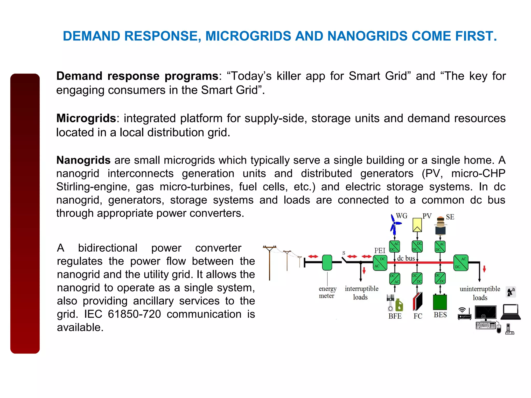

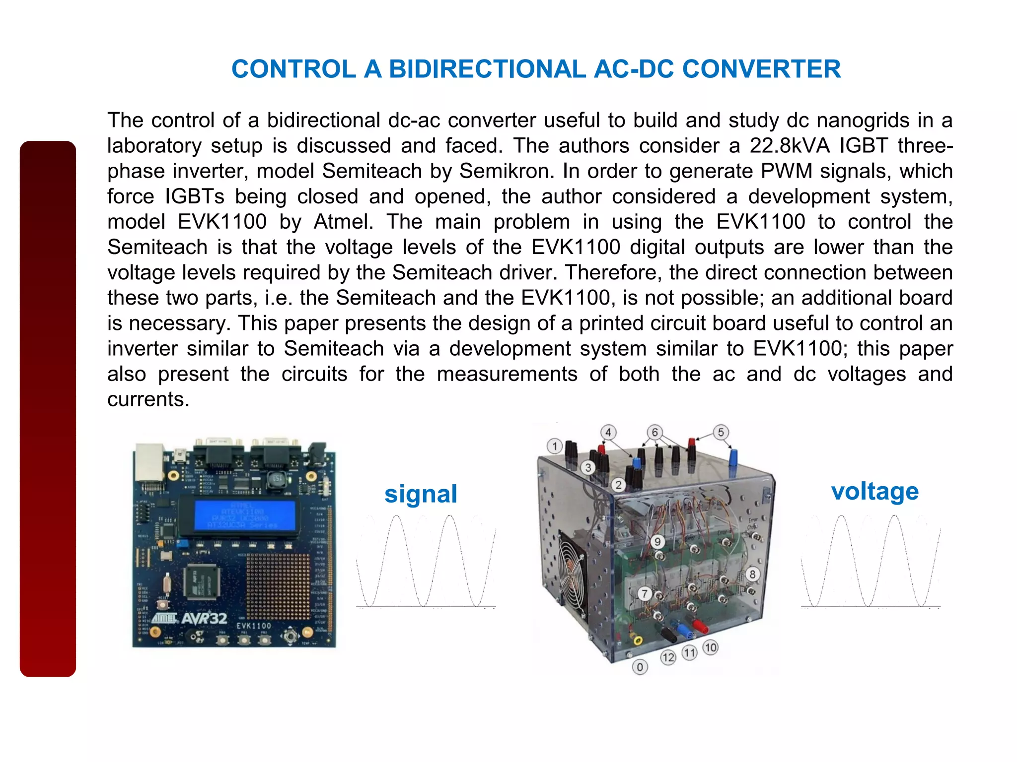
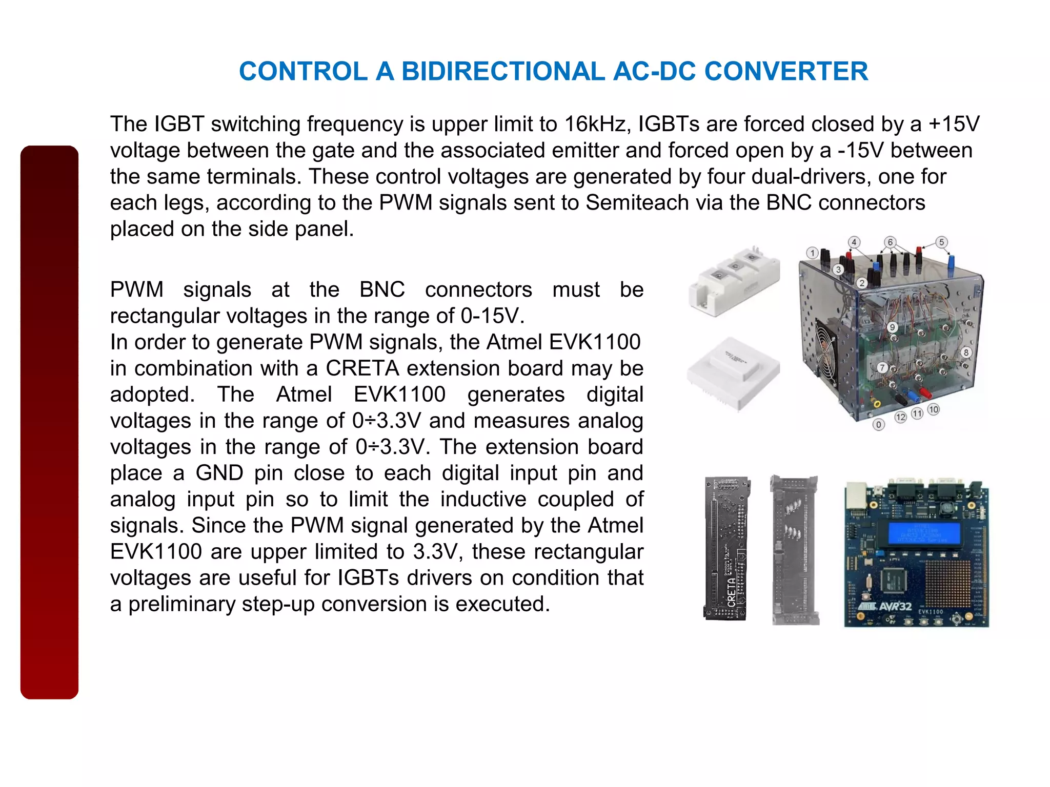

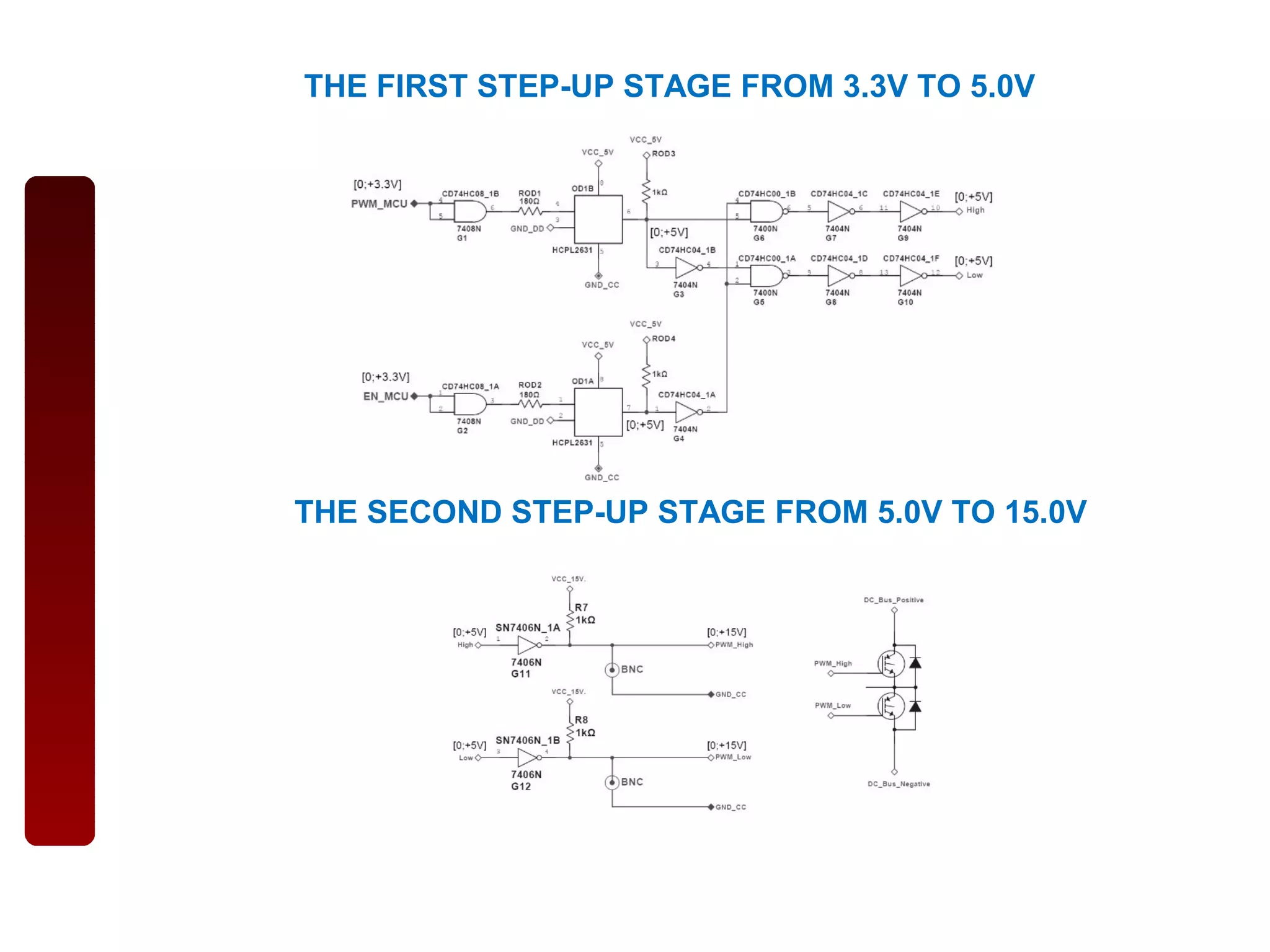
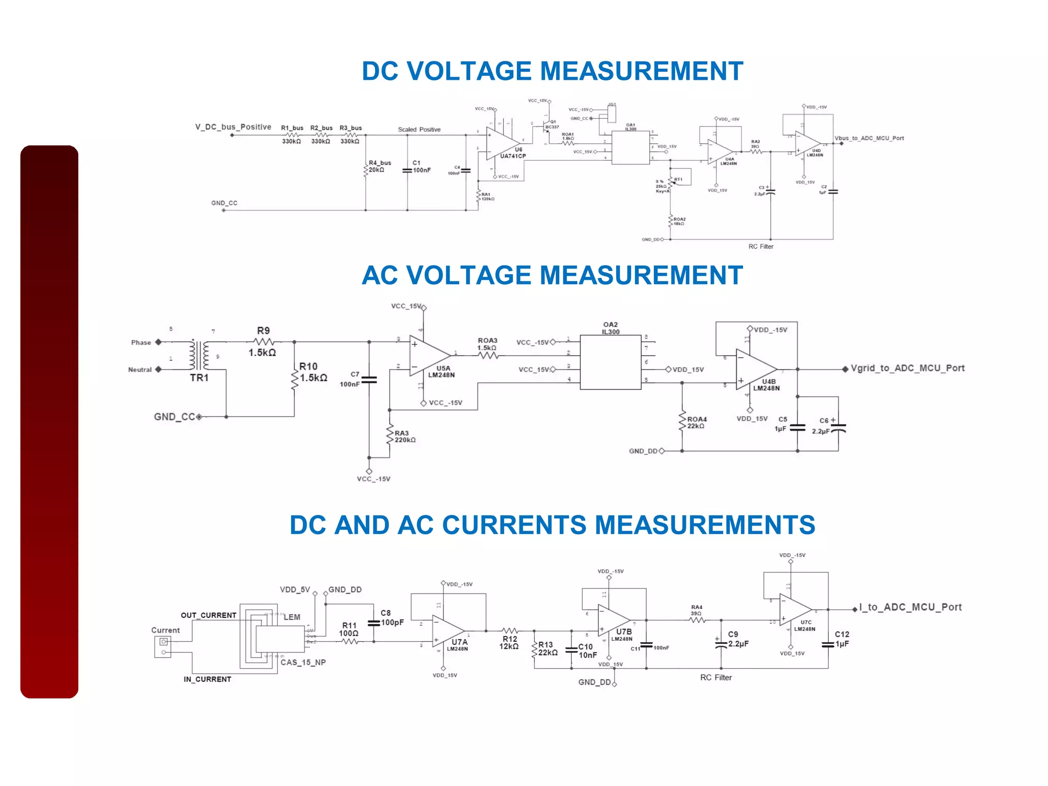
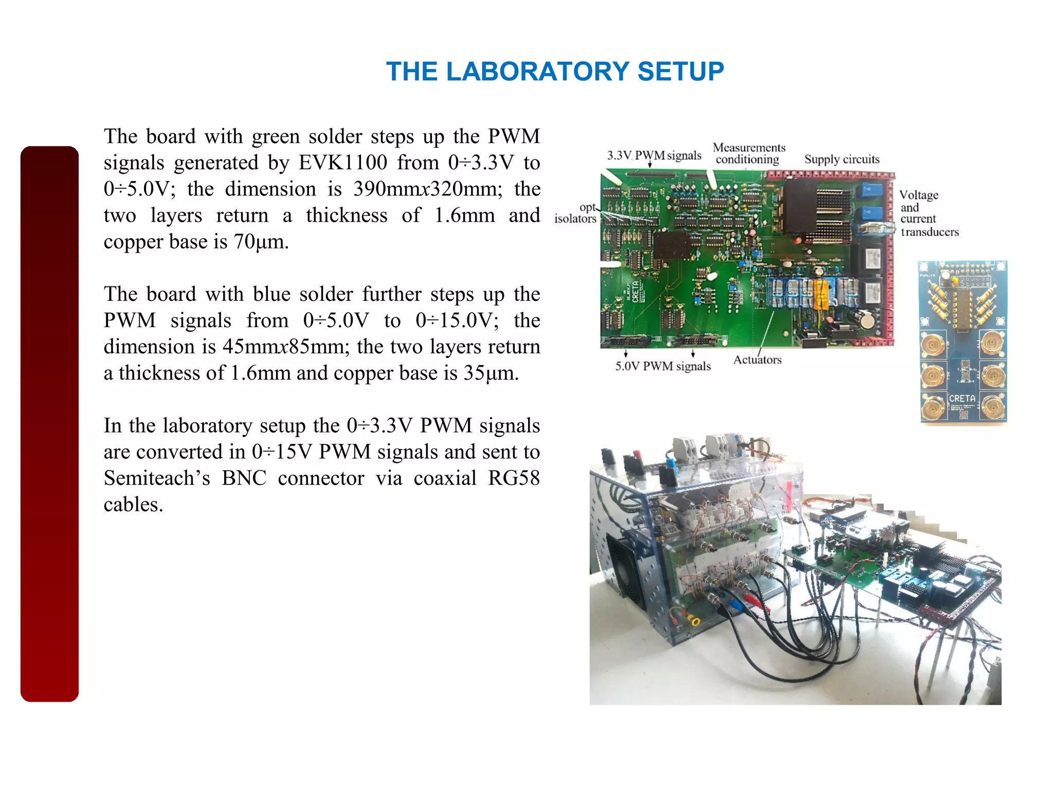
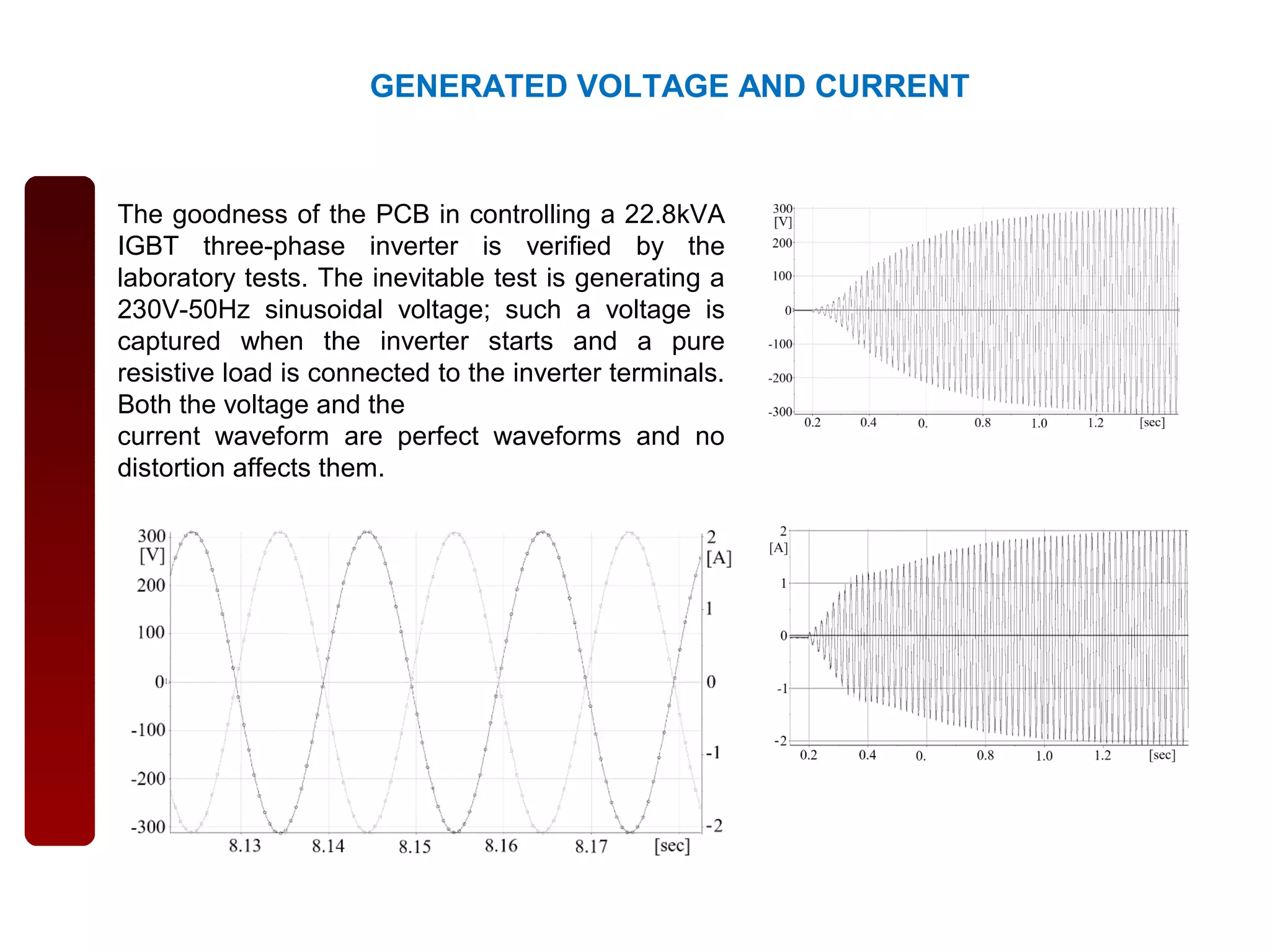


The document discusses the design and implementation of a printed circuit board for controlling a 22.8kVA IGBT three-phase inverter in a laboratory setting focused on DC nanogrids. It highlights the integration of various energy sources within microgrids and nanogrids, emphasizing the role of collaborative energy systems and demand response programs in engaging consumers. Key technical details are provided regarding signal control, circuit design, and the successful laboratory tests verifying the performance of the developed inverter control system.