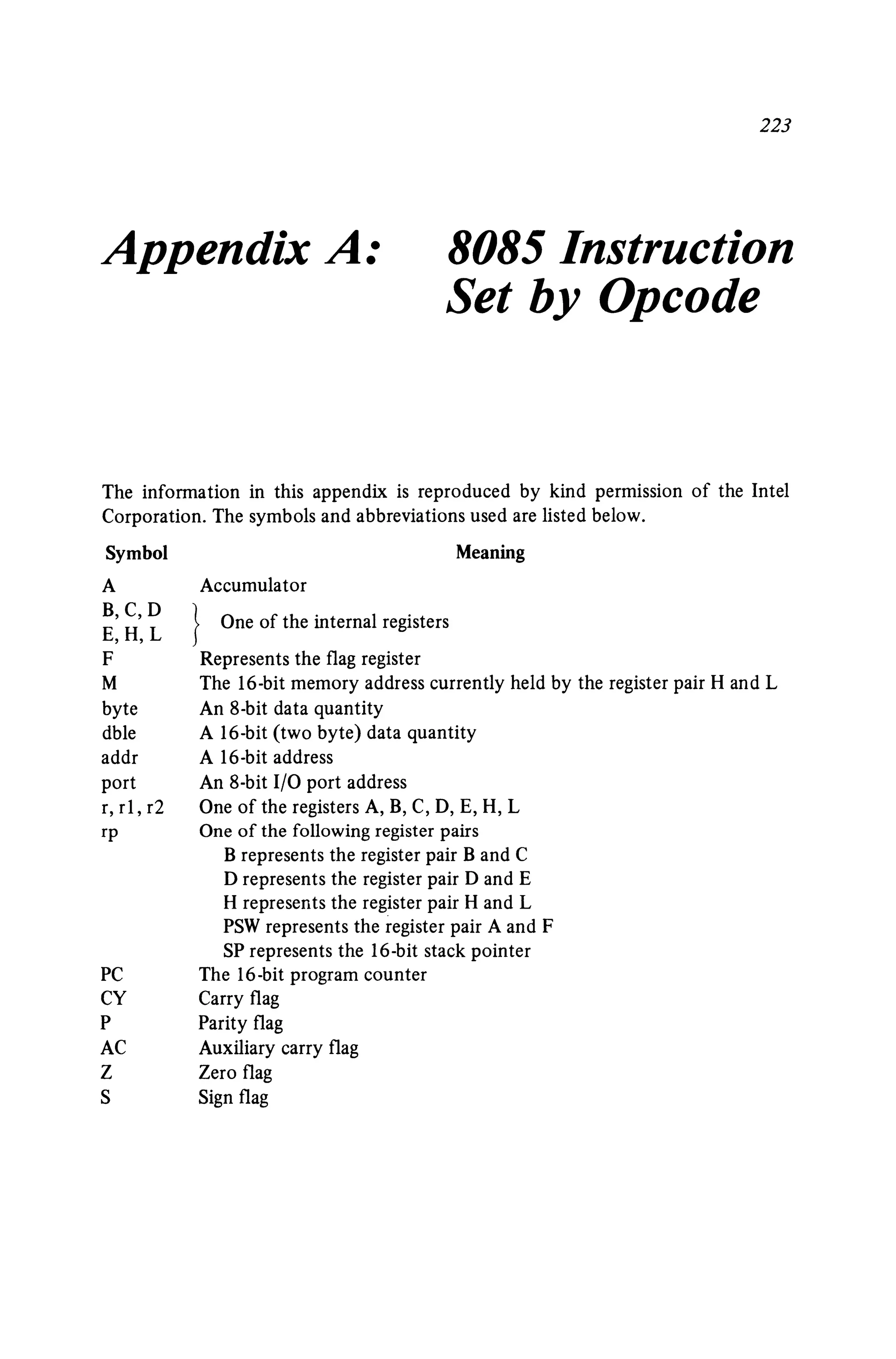
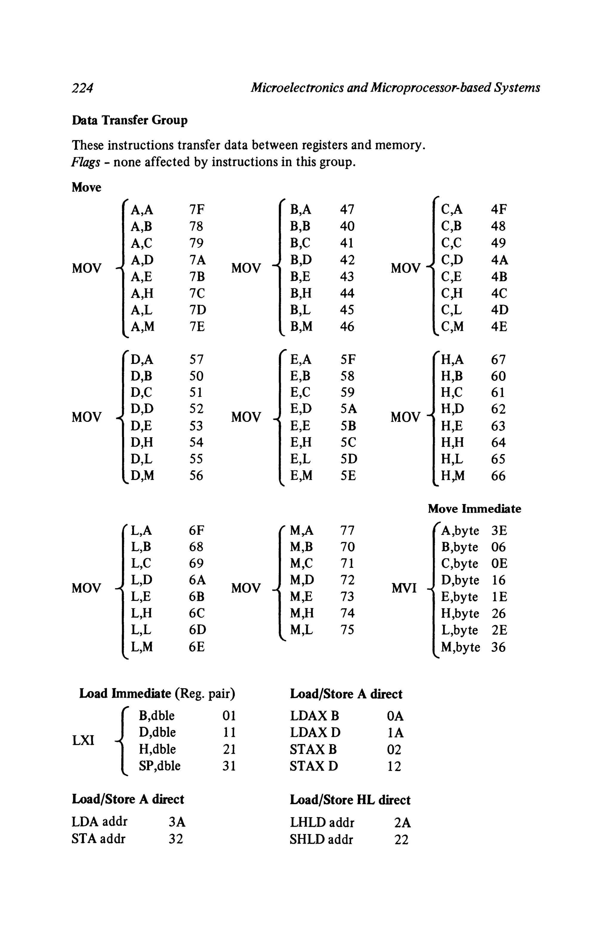
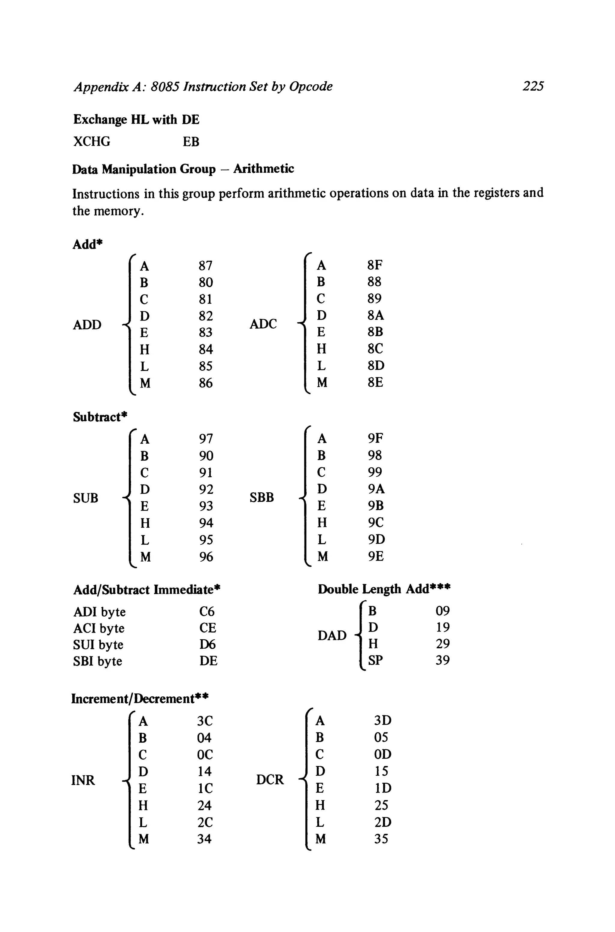
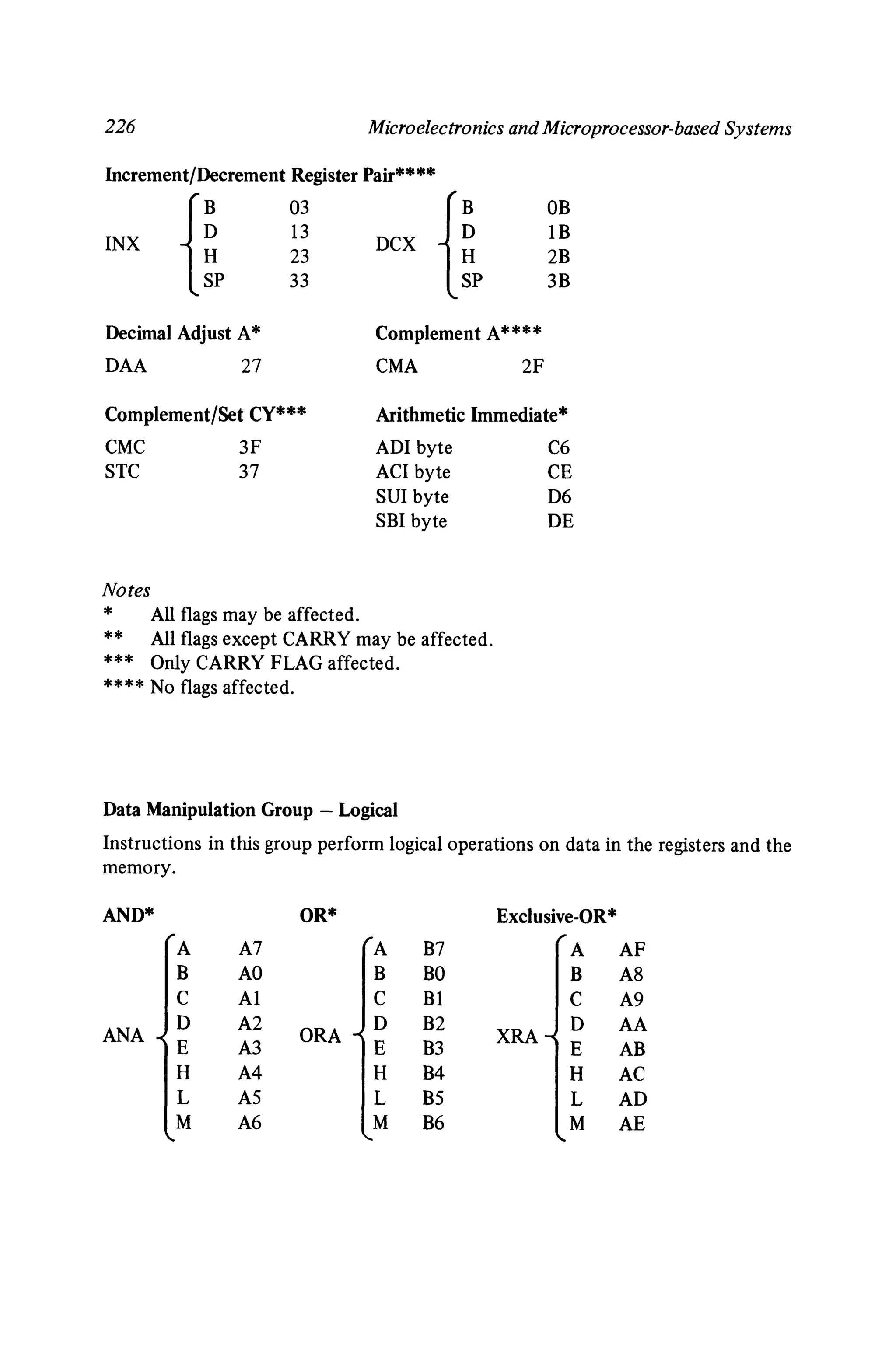
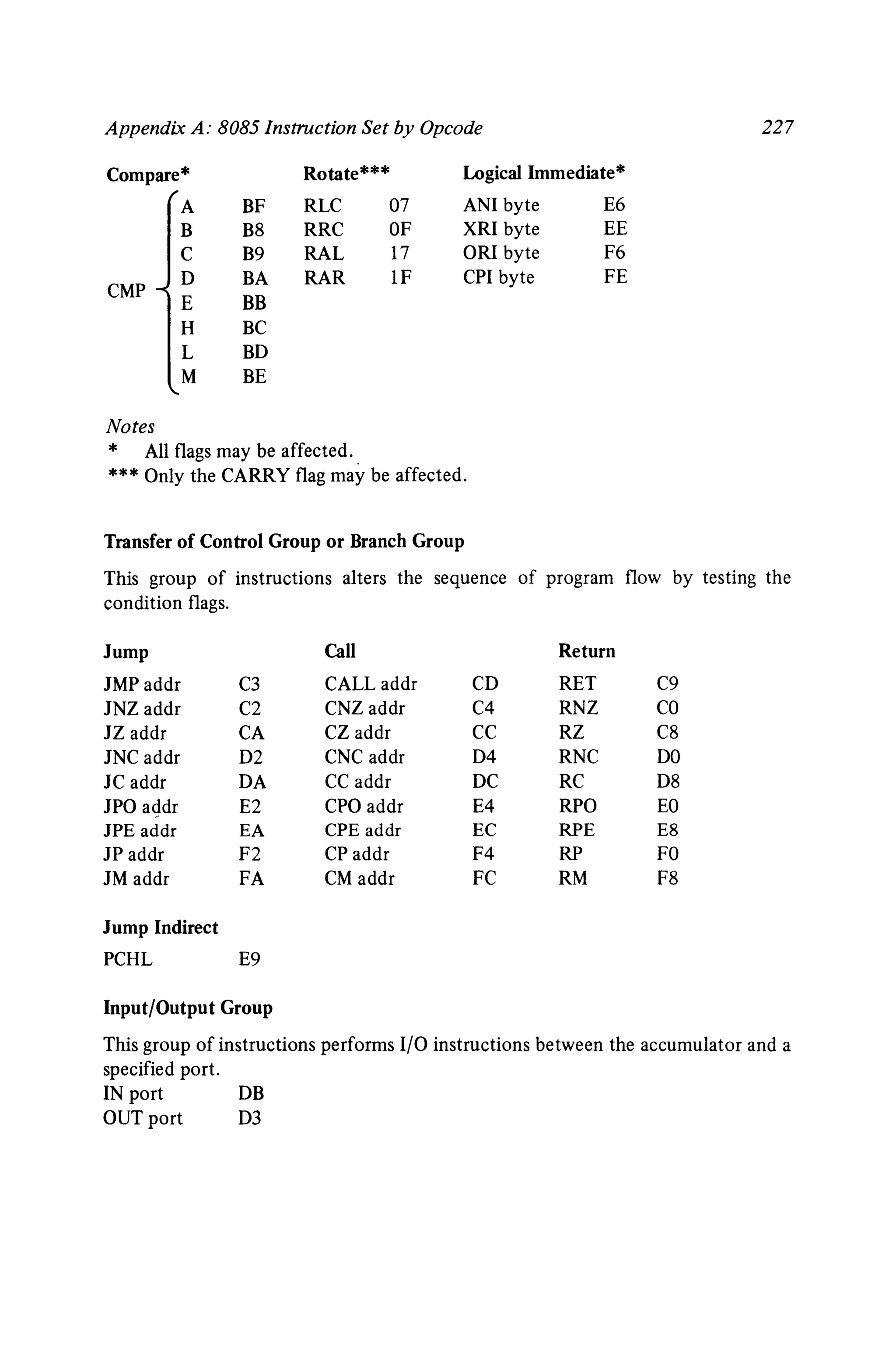
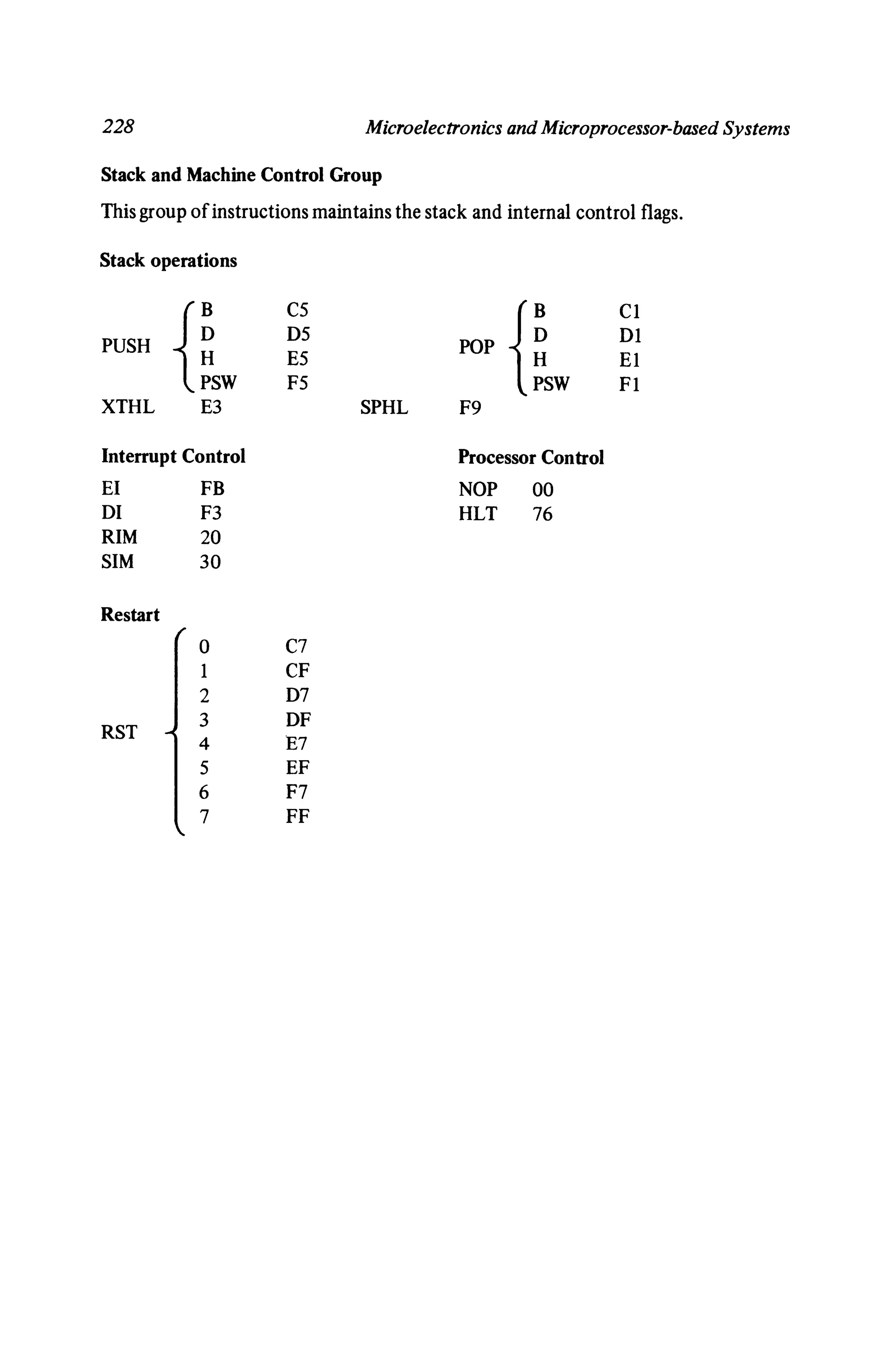
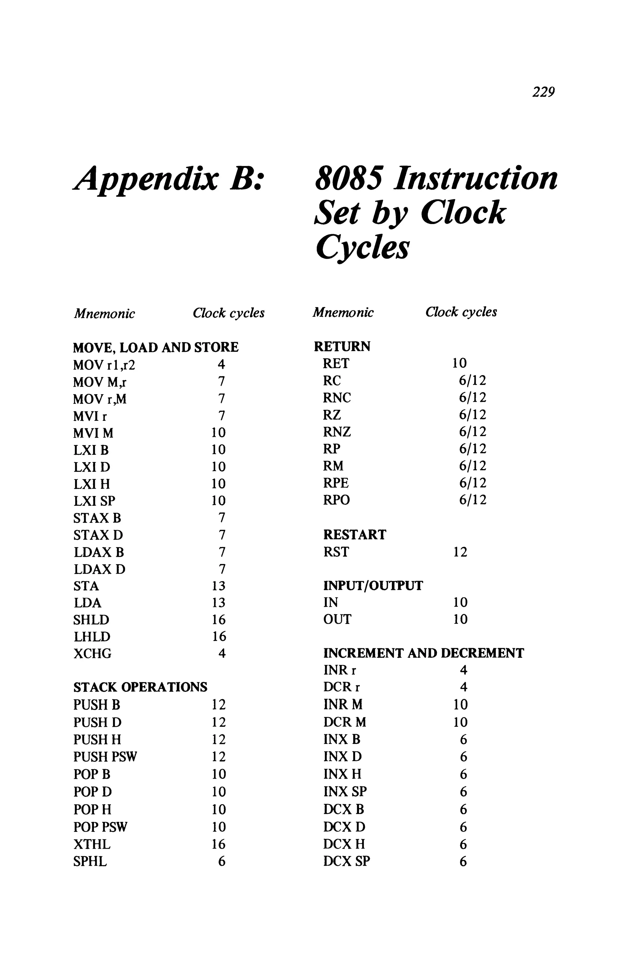
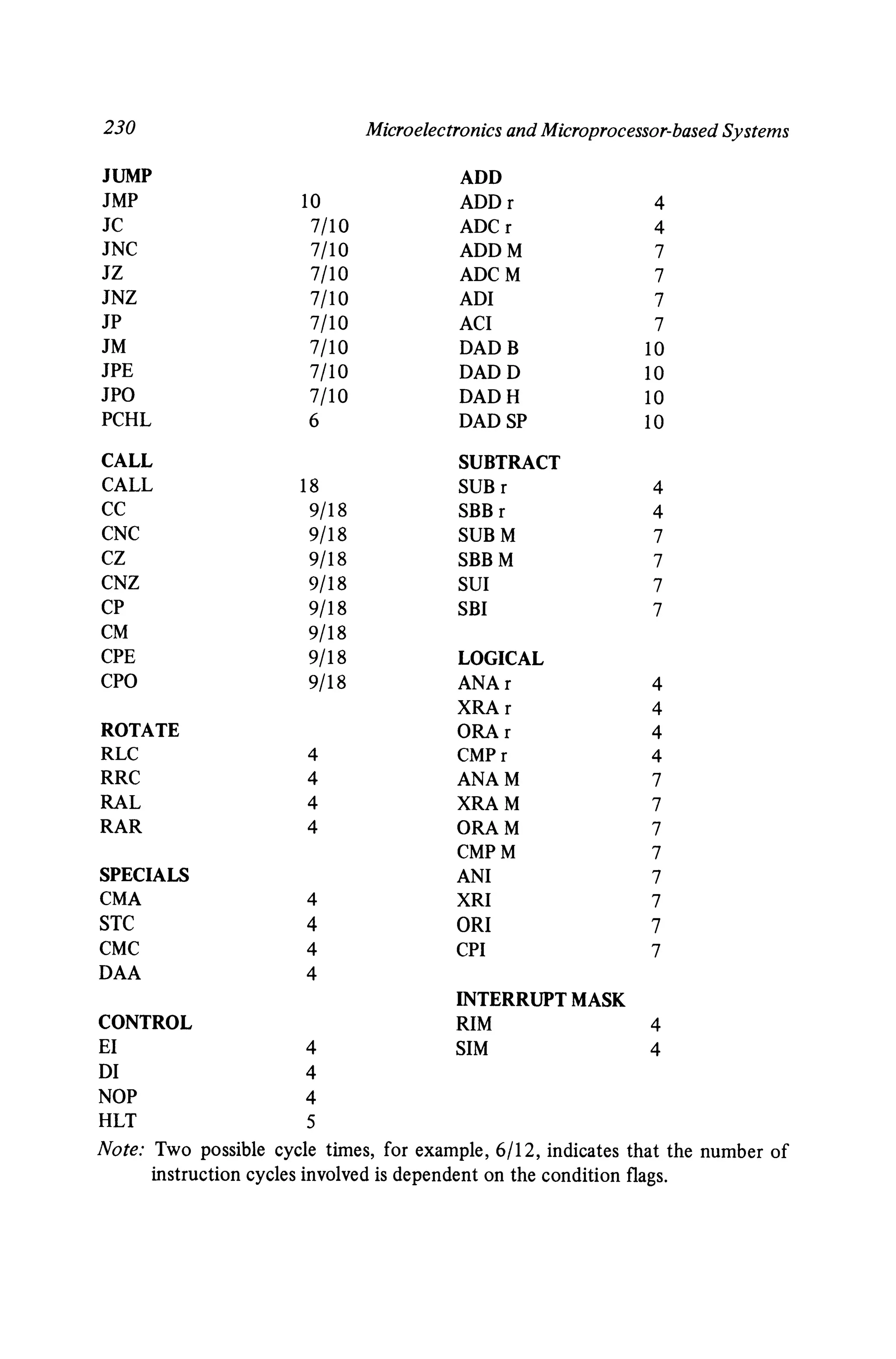
SlideShare a Scribd company logo
1 of 16
Download to read offline
Appendix A:
223
8085 Instruction
Set by Opcode
The information in this appendix is reproduced by kind permission of the Intel
Corporation. The symbols and abbreviations used are listed below.
Symbol
A
B,C,D
E,H,L
F
M
byte
dbIe
addr
port
r, rl, r2
rp
PC
CY
P
AC
Z
S
Meaning
Accumulator
} One of the internal registers
Represents the flag register
The 16-bit memory address currently held by the register pair Hand L
An 8-bit data quantity
A 16-bit (two byte) data quantity
A 16-bit address
An 8-bit I/O port address
One of the registers A, B, C, D, E, H, L
One of the following register pairs
B represents the register pair Band C
D represents the register pair D and E
H represents the register pair Hand L
PSW represents the register pair A and F
SP represents the 16-bit stack pointer
The 16-bit program counter
Carry flag
Parity flag
Auxiliary carry flag
Zero flag
Sign flag
224 Microelectronics andMicroprocessor-based Systems
Data Transfer Group
These instructions transfer data between registers and memory.
Flags - none affected by instructions in this group.
Move
A,A 7F B,A 47 C,A 4F
A,B 78 B,B 40 C,B 48
A,C 79 B,C 41 C,C 49
MaV
A,D 7A
MaV
B,D 42
MaV
C,D 4A
A,E 7B B,E 43 C,E 4B
A,H 7C B,H 44 C,H 4C
A,L 7D B,L 45 C,L 4D
A,M 7E B,M 46 C,M 4E
D,A 57 E,A SF H,A 67
D,B 50 E,B 58 H,B 60
D,C 51 E,C 59 H,C 61
MaV
D,D 52
MaV
E,D SA
MaV
H,D 62
D,E 53 E,E 5B H,E 63
D,H 54 E,H 5C H,H 64
D,L 55 E,L 5D H,L 65
D,M 56 E,M 5E H,M 66
Move Immediate
L,A 6F M,A 77 A,byte 3E
L,B 68 M,B 70 B,byte 06
L,C 69 M,C 71 C,byte OE
MaV
L,D 6A
MaV
M,D 72
MYI
D,byte 16
L,E 6B M,E 73 E,byte IE
L,H 6C M,H 74 H,byte 26
L,L 6D M,L 75 L,byte 2E
L,M 6E M,byte 36
Load Immediate (Reg. pair) Load/Store A direct
{ B,db!, 01 LDAXB OA
LXI
D,dble 11 LDAXD lA
H,dble 21 STAXB 02
SP,dble 31 STAXD 12
Load/Store A direct Load/Store HL direct
LDA addr 3A LHLD addr 2A
STA addr 32 SHLDaddr 22
Appendix A: 8085 Instruction Set by Opcode 225
Exchange HL with DE
XCHG EB
Data Manipulation Group - Arithmetic
Instructions in this group perform arithmetic operations on data in the registers and
the memory.
Add*
A 87 A 8F
B 80 B 88
C 81 C 89
ADD
D 82
ADC
D 8A
E 83 E 8B
H 84 H 8C
L 85 L 8D
M 86 M 8E
Subtract*
A 97 A 9F
B 90 B 98
C 91 C 99
SUB
D 92
SBB
D 9A
E 93 E 9B
H 94 H 9C
L 95 L 9D
M 96 M 9E
Add/Subtract Immediate* Double Length Add***
ADI byte C6
DAD {~
09
ACI byte CE 19
SUI byte D6 29
SBI byte DE SP 39
Increment/Decrement**
A 3C A 3D
B 04 B 05
C OC C OD
INR
D 14
DCR
D 15
E lC E 10
H 24 H 25
L 2C L 2D
M 34 M 35
226 Microelectronics and Microprocessor-based Systems
Increment/Decrement Register Pair****
U
03
Hp
OB
INX
13
DCX
IB
23 2B
33 3B
Complement AU**
Decimal Adjust A*
DAA 27 CMA 2F
Complement/Set CY***
CMC 3F
STC 37
Arithmetic Immediate*
AD! byte C6
ACI byte CE
SUI byte D6
SBI byte DE
Notes
* All flags may be affected.
** All flags except CARRY may be affected.
*** Only CARRY FLAG affected.
**** No flags affected.
Data Manipulation Group - Logical
Instructions in this group perform logical operations on data in the registers and the
memory.
AND* OR* Exclusive-OR*
A A7 A B7 A AF
B AO B BO B A8
C Al C Bl C A9
ANA
D A2
ORA
D B2
XRA
D AA
E A3 E B3 E AB
H A4 H B4 H AC
L AS L B5 L AD
M A6 M B6 M AE
Appendix A: 8085 Instruction Set by Opcode 227
CMP
Compare*
A
B
C
D
E
H
L
M
BF
B8
B9
BA
BB
BC
BD
BE
Rotate***
RLC 07
RRC OF
RAL 17
RAR IF
Logical Immediate*
ANI byte E6
XRI byte EE
ORI byte F6
CPI byte FE
Notes
* All flags may be affected.
*** Only the CARRY flag may be affected.
Transfer of Control Group or Branch Group
This group of instructions alters the sequence of program flow by testing the
condition flags.
Jump Call Return
IMP addr C3 CALL addr CD RET C9
INZ addr C2 CNZ addr C4 RNZ CO
IZ addr CA CZ addr CC RZ C8
INC addr D2 CNC addr D4 RNC DO
IC addr DA CC addr DC RC D8
IPO addr E2 CPO addr E4 RPO EO
JPE addr EA CPE addr EC RPE E8
IP addr F2 CP addr F4 RP FO
1M addr FA CM addr FC RM F8
Jump Indirect
PCHL E9
Input/Output Group
This group of instructions performs I/O instructions between the accumulator and a
specified port.
IN port DB
OUT port D3
228 Microelectronics and Microprocessor-based Systems
Stack and Machine Control Group
Thisgroup ofinstructions maintains the stack and internal control flags.
Stack operations
{L
C5
{L
CI
PUSH
D5
POP
D1
E5 EI
F5 FI
XTHL E3 SPHL F9
Interrupt Control Processor Control
EI FB NOP 00
DI F3 HLT 76
RIM 20
SIM 30
Restart
0 C7
1 CF
2 D7
RST
3 DF
4 E7
5 EF
6 F7
7 FF
Appendix B:
229
8085 Instruction
Set by Clock
Cycles
STACK OPERATIONS
PUSH B 12
PUSH D 12
PUSH H 12
PUSH PSW 12
POP B 10
POP D 10
POP H 10
POPPSW 10
XTHL 16
SPHL 6
MOVE, LOAD AND STORE
MOV rl,r2 4
MOVM,r 7
MOVr,M 7
MVI r 7
MVI M 10
LXI B 10
LXID 10
LXI H 10
LXI SP 10
STAXB 7
STAXD 7
LDAX B 7
LDAX D 7
STA 13
LDA 13
SHLD 16
LHLD 16
XCHG 4
Mnemonic Clock cycles Mnemonic Clock cycles
RETURN
RET 10
RC 6/12
RNC 6/12
RZ 6/12
RNZ 6/12
RP 6/12
RM 6/12
RPE 6/12
RPO 6/12
RESTART
RST 12
INPUT/OUTPUT
IN 10
OUT 10
INCREMENT AND DECREMENT
INRr 4
DCRr 4
INR M 10
DCRM 10
INXB 6
INXD 6
INXH 6
INX SP 6
DCXB 6
DCXD 6
DCXH 6
DCX SP 6
230 Microelectronics and Microprocessor-based Systems
JUMP ADD
1MP 10 ADDr 4
1C 7/10 ADCr 4
1NC 7/10 ADDM 7
1Z 7/10 ADCM 7
1NZ 7/10 ADI 7
1P 7/10 ACI 7
1M 7/10 DADB 10
1PE 7/10 DADD 10
1PO 7/10 DADH 10
PCHL 6 DADSP 10
CALL SUBTRACT
CALL 18 SUBr 4
CC 9/18 SBB r 4
CNC 9/18 SUBM 7
CZ 9/18 SBBM 7
CNZ 9/18 SUI 7
CP 9/1 8 SBI 7
CM 9/18
CPE 9/18 LOGICAL
CPO 9/18 ANAr 4
XRAr 4
ROTATE ORAr 4
RLC 4 CMP r 4
RRC 4 ANAM 7
RAL 4 XRA M 7
RAR 4 ORAM 7
CMP M 7
SPECIALS ANI 7
CMA 4 XRI 7
STC 4 ORI 7
CMC 4 CPI 7
DAA 4
INTERRUPTMASK
CONTROL RIM 4
EI 4 SIM 4
DI 4
NOP 4
HLT 5
No te: Two possible cycle times, for example, 6/12, indicates that the number of
instruction cycles involved is dependent on the condition flags.
231
Solutions to Problems
l.l (a) 3548 , (b) 0111011002 , (c) OECH.
1.2 (a) 1110112 , (b) 153l8,(c) 1245H.
1.3 (a) 2730 , (b) 156, (c) 85.
1.4 (a) 10001000010002 , (b) 104108 , (c) 1108H.
1.5 (a) - 86, (b) - 85.
1.6 (a) 00000101 , (b) 111110ll ,(c) Ill00110,(d) 10110000.
1.7 (a) 65 535, (b) +32767 and - 32 768.
1.8 Both the carry and overflow flags are 'set' to '1'.
2.9 4K locations.
2.11 ROM A = ROM B = tK.
RAM C =RAM D =RAM E =RAM F =tK.
System expansion blocks = lK each.
5.5 (a) 2K, (b) (i) OOOOH, (b) (ii) 07FFH.
5.6 (a) F800H, (b) FFFFH.
7.2 219100rDBH.
7.3 3.28 ms.
9.15 MVI H,OO
MVI L,byte
LXI D,2000H
DADD
MOV A,M
STA 200FH
HLT
; HIGH BYTE OF INDEX ADDRESS =OOH
; LOWBYTE OF INDEX ADDRESS IN L
; BASE ADDRESS OF TABLE IN D AND E
; FORM EFFECTIVE ADDRESS OF RESULT
; GET PETHERICK CODE FROM TABLE
; STORE IT IN 200FH
; HALT
10.4 COUNT 1 = 21910 or DBH, COUNT 2 = 19910 or C7H.
(Note: in general the value of the product COUNT 1 x COUNT 2 =43 581 10 ,)
11.7 (a)
PC 2060
SP 20AE
(b)
2080
20AC
(c) (d)
20AO 208C
20AA 20AC
(e)
2068
20AE
(f)
2025
20BO
232 Microelectronics and Microprocessor-based Systems
12.3
Address Byte Label Instruction Comment
mnemonic
I 2 3
2010 3EOl MYI A,OlH
2012 D3 20 OUT20H ; INITIALISE PIO
2014 31 BO 20 LXI SP,20BOH ; INITIALISE STACK POINTER
2017 DB 22 IN 20H ; READ SWITCHES
2019 2F CMA ; COMPLEMENT DATA
20 l A 3200 20 LOOP: STA 2000H ; STORE DATA IN 2000H
20 ID D3 21 OUT 21H ; DISPLAY DATA ON LEDs
20 l F CD 09 03 CALL TIME ; CALL TIME DELAY
2022 DBn IN22H ; READ SWITCHES
2024 A7 ANA A ; SET FLAGS
2025 C2 IA 20 JNZ LOOP ; RETURN TO LOOP IF ANY
; SWITCH = I
2028 D3 21 OUT 21H ; EXTINGUISH LEDS
202A 76 HLT ; HALT PROGRAM
12.4
Label
START:
Instruction
mnemonic
LXI SP,20BOH
MYI A,OIH
OUT 20H
IN 22H
STA 2000H
CALL 03DFH
LDA 2000H
XRIOFH
OUT 21H
JMPSTART
Comment
; INITIALISE STACK POINTER
; INITIALISE PIO
; READ STATE OF SWITCHES
; STORE DATA IN LOCATION
2000H
; DISPLAY DATA ON YDU
; RECALL DATA
; INVERT LOW BYTE OF DATA
; DISPLAY RESULT ON LEDS
; READ SWITCHES ONCE AGAIN
14.5 0010H, 0020H , 0024H , 003CH.
14.6 Yes.
14.8 LXI SP,20BOH ; INITIALISE STACK POINTER
MYI A,OCH ; UNMASK RST 6.5 AND 5.5
SIM
EI ; ENABLE INTERRUPTS
Solutions to Problems
14.9
233
Address Byte
1 2 3
Label Instruction
mnemonic
Comment
2020 0604
2022 21 0020
2025 97
2026 86
2027 23
2028 05
2029 C2 26 20
202C 320420
202F 76
2030 C3 3020
MVI B,04H ; LOAD COUNTER
LXI H,2000H ; POINTER M = 2000H
SUB A ; CLEAR ACCUMULATOR
LOOP: ADD M ; FORM SUM IN ACCUMULATOR
INX H ; INCREMENT POINTER
OCR B ; DECREMENT COUNTER
JNZ LOOP ; JUMP IF SUM NOT COMPLETE
STA 2004H ; STORE SUM
HLT ; WAIT FOR INTERRUPT
STOP: JMP STOP ; TERMINATE PROGRAM
2080 3A 0420
2083 07
2084 07
2085 E6 FC
2087 320520
208B C9
INTR: LDA 2004H
RLC
RLC
ANIFC
STA 2005H
RET
; GET SUM
; ROTATE DATA LEFT TWICE
; TO MULTIPLY BY FOUR
; MASK OUT NON-SIGNIFICANT BITS
; STORE PRODUCT
; INTERRUPT NEED NOT BE RE-
ENABLED
; RETURN TO MAIN PROGRAM
14.10 (a) 5.325 ms (b) 21.3 ms.
234
Index of Useful Programs
Table
9.4
9.5
9.7
10.1
10.4
10.5
11.6
11.8
12.2
12.3
12.5
12.6
12.11
13.2
13.3
13.4
13.6
14.2
14.3
14.6
14.7
14.8
14.9
14.10
Program
Hexadecimal addition program
Decimal addition program
'Squares' program using a lookup table
Program that adds five hex values
Short time delay program
Nested time delay
Simple subroutine
Simple nested subroutines
Digital input and output of data
Flashing light sequence
Direct control of a stepper motor
Stepper motor control using a special 'driver' integrated circuit
Handshake program using two handshake lines
Square wave program
Ramp waveform program
Generating a waveform using a 'lookup' table
Program for a successive approximation ADC
Typical RST 6.5 initialisation procedure
A program containing an interrupt (RST 6.5)
An elapsed time interrupt
A handshake data transfer - polled interrupts
Interrupt-driven handshake, main program
Interrupt-driven handshake, input handshake (RST 5.5)
Interrupt-driven handshake, output handshake (RST 6.5)
112
113
115
120
127
129
138
142
150
151
155
158
168
176
177
179
187
203
206
213
218
220
220
220
Index
Accumulator 28
Accumulator I/O addressing 24
Addition 6
binary 7
double-length 88
hexadecimal 8
Address 18
Address bus I 8
Address decoding 45-58
Address field III
Address/data bus 32
Addressing mode 102
direct 105
extended 105
immediate 102
implied 104
indexed 106, 114
indirect 106
inherent 104
register direct 106
register indirect 107
relative 109
stack 106
zero page 106
Algorithm 82
Analogue-to-digital convertor (ADC)
179
continuous balance 182
interfacing to 188-94
successive-approximation 183-8
Architecture of CPU 28
Arithmetic and logic instructions 96
Arithmetic and logic unit (ALU) 14, 30
Arithmetic shift 100
Assembier statement 110
Assembly language 94, 110
Auxiliary carry flag 30
235
Base I
Baud rate 74
Bidirectional data bus 18
Binary digit (bit) 2
Binary number I
Bit time 74
Branch instructions see Jump
instructions
Break point 93
Buffer 60
Bus system 18, 26
Byte 12
Call instruction 132
Carry flag 9, 29 , 30
auxiliary 30
Central processing unit (CPU) 14
Chip IS
Chip enable pin 20 ,25
Chip select pin 20, 46 , 47
Clock oscillator 16, 31, 35
Code conversion 116
Comment, in program III
Comparison instruction 98
Complement, binary 9
Conditional call instructions 132
Conditional jump instructions 101
Conditional return instructions 132
Control and timing section 31
Control bus 18
Control unit of CPU 14
CIS register of PIO 147
command aspect of 147,148,
164
status aspect of 166
236
Data bus 18
Data manipulation instructions 95
Data rate 76
Data transfer instructions 95
Debugging 90
Decimal adjustment instruction 112 ,
113
Decoder 46-57
Dedicated microcomputer 14
Delay (time) routine 78-80, 125-9
Device enable pin 20
Device select pin 20
Digital computer 14
Digital input and output 148
Digital-to-analogue convertor (DAC)
173-9
waveform generation using 175
Direct digital control (DDC) 152
Displacement 108
Dual-in-line package (DIP) IS
Dynamic RAM 44
Effective address 108 , 114
EPROM 16, 17
Fetch--execute cycle 33
Field structure, of assembly language
instruction 110-13
FIFO store 44
Firmware 18
Flag 9,29
Flag register 9, 29
Flip-flop 9
Flowchart 82
Foldback, on memory map 57
Full-adder 7
General-purpose computer 14
Half-carry flag see Auxiliary carry flag
Handshake 42 , 159-69
implementing 161
input 160 ,163
output 160 , 163
Hardware 17
Hexadecimal numbers 3
Index (in addressing mode) 114
Index register 108
Input/output port 17,20, 23
bidirectional 22
dedicated 17
programmable 17, 145-8
unidirectional 22
Instruction decoder 31
Instruction register 30
Instruction set 94,223,229
Integrated circuit IS
Interface 17, 60
Interrupt 41 , 196
handshake 214-21
maskable 196
multilevel 206
non-maskable 41 , 196
polled 197 , 217
priority of 200
timer (PIO) 209
vectored 197 , 199
8085 198
Interrupt flag 197
Interrupt handling 202
Interrupt mask (I register) 200
Interrupt routine 41
Interval timer 78
I/O control module 148, 149
I/O read 39
I/O timing 39
I/O write 37
Jump instructions 101
Keyboard 67-73
Label , in program 86 ,94, III
Latched I/O port 63-7,70
LED,7-segment 63-8
LIFO store 44 , 106 , 134
Listener, in handshake 160
Index
Index
Logical instructions 96-100
Logical shift 100
Lookuptable 113-16,178,179
Loop, in program 118
Machine code instruction 94,95,109
Machine cycle 35
Mainframe computer 14
Maskable interrupt 196
Memory 14
Memory access time 39
Memory map 23
Memory read 38
Memory register 28
Memory write 36
Memory-mapped address 24
Memory-mapped I/O 24
Microcomputer 14
Microcycle 35
Microprocessor-based system 14, 18
minimal 17
Minicomputer 14
Monitor program 92
Multiplexing 32
Negative flag 30
Negative number, binary 9, 10
Non-maskable interrupt 41 , 196
Non-volatile memory 44
Number conversion 4-6
Octal number 2
Offset 108, 114
One's complement 9, 10
Opcode 30 ,90, III
Operand 14
Operand field , in assembly program
III
Operation code 30,90
Output port 20-3
Overflow 12
Overflow flag 12
23 7
Page 23
Parallel I/O port 20-3
Parameter passing 143
Parity flag 29,30
Peripheral 17
Pointer register 28,105
Polling 40, 217
POP instruction 135-7
Port 17,20,33,145
Processor status word (PSW) 137
Program 14, 17,82
Program counter 28
Programmable I/O port 17, 145-8
timer in 209
Programmable timer 80
Pseudo-operation 112
PUSH instruction 135-7
Radix 1
RAM (random-access memory) 16,44
Read signal 31
Read-write memory 16
Real-time clock 78
Register 28
Return instruction 132
Rollover (keyboard) protection 70
ROM (read-only memory) 16,47
Rotate instruction 98
Serial I/O port 20,23,73
Seven-segment display 63-8
Sign bit 9
Sign flag 30
Signed binary num ber 9
Single stepping 93
Software 17
Stack 134
Stack pointer 29, 135
State, timing 35
Static RAM 44
Status register see Flag register
Stepper motor 152-9
Store 14
Strobed data transfer 159
Structured programming 82-7
23 8
Subroutine 132 ,149
nested 140
Subroutine call 102
Subroutine return 102
Subroutine structure 133
Subtraction, binary 10, 11
Successive-approximation ADC 183-8
Symbolic address (lab el) 86 ,94
Talker, in handshake 159
Test and bran ch instructions 101
Three-stat e (tri-state) gate 24-6 ,60
Time delay program 78-80 ,125-7,
151
nested I27-9
Timer (PIO or hardware) 209
Timing sequences 78
Trace rou tine 90
Index
Trace table 89 ,92,139
T-state 35
Two's complement 10, II
UART 73
Unconditional jump instruction 101
Unsigned binary number 8, 11
Vectored interrupt 197 ,199
Video display unit (V DU) 18
Volatile memory 44
Write signal 31
Zero flag 30

More Related Content

Similar to Here are some of the most useful programs from the index:- Hexadecimal addition program (Table 9.4) - Demonstrates adding two hex numbers in memory locations. Useful for learning hex arithmetic. - Decimal addition program (Table 9.5) - Same as above but for decimal numbers, good for reinforcement.- 'Squares' program using a lookup table (Table 9.7) - Shows how to use a pre-calculated table to look up values, like for mathematical functions. - Short time delay program (Table 10.5) - Basic timing/delay functionality needed for many programs. - Digital input and output of data (Table 12.2) - Simple I/O to

74LS47 / DM74LS47 Datasheet PDF
74LS47 / DM74LS47 Datasheet PDF74LS47 / DM74LS47 Datasheet PDF
74LS47 / DM74LS47 Datasheet PDFDatasheet
 
Microprocessor lab manual
Microprocessor lab manualMicroprocessor lab manual
Microprocessor lab manualDhaval Shukla
 
1203 Ppi 8155
1203 Ppi 81551203 Ppi 8155
1203 Ppi 8155techbed
 
TRAFFIC LIGHT CONTROL SYSTEM USING 8085 MICROPROCESSOR
TRAFFIC LIGHT CONTROL SYSTEM USING 8085 MICROPROCESSORTRAFFIC LIGHT CONTROL SYSTEM USING 8085 MICROPROCESSOR
TRAFFIC LIGHT CONTROL SYSTEM USING 8085 MICROPROCESSORSubash Sambath Kumar
 
Assembly Language Programming Of 8085
Assembly Language Programming Of 8085Assembly Language Programming Of 8085
Assembly Language Programming Of 8085techbed
 
Basic programming of 8085
Basic programming of 8085 Basic programming of 8085
Basic programming of 8085 vijaydeepakg
 
7447_datasheet.pdf© 2001 Fairchild Semiconductor Corporati.docx
7447_datasheet.pdf© 2001 Fairchild Semiconductor Corporati.docx7447_datasheet.pdf© 2001 Fairchild Semiconductor Corporati.docx
7447_datasheet.pdf© 2001 Fairchild Semiconductor Corporati.docxalinainglis
 
Microprocessorandmicroconrollermcq3 121116120640-phpapp02
Microprocessorandmicroconrollermcq3 121116120640-phpapp02Microprocessorandmicroconrollermcq3 121116120640-phpapp02
Microprocessorandmicroconrollermcq3 121116120640-phpapp02Yazeed Khalid
 
microp-8085 74 instructions for mct-A :P
microp-8085 74 instructions for mct-A :Pmicrop-8085 74 instructions for mct-A :P
microp-8085 74 instructions for mct-A :PJathin Kanumuri
 
8085 Paper Presentation slides,ppt,microprocessor 8085 ,guide, instruction set
8085 Paper Presentation slides,ppt,microprocessor 8085 ,guide, instruction set8085 Paper Presentation slides,ppt,microprocessor 8085 ,guide, instruction set
8085 Paper Presentation slides,ppt,microprocessor 8085 ,guide, instruction setSaumitra Rukmangad
 
microp-8085 74 instructions for mct-A :P-2
microp-8085 74 instructions for mct-A :P-2microp-8085 74 instructions for mct-A :P-2
microp-8085 74 instructions for mct-A :P-2Jathin Kanumuri
 
8085 instruction set
8085 instruction set8085 instruction set
8085 instruction setJLoknathDora
 
2. 8085-Microprocessor.pptx
2. 8085-Microprocessor.pptx2. 8085-Microprocessor.pptx
2. 8085-Microprocessor.pptxISMT College
 

Similar to Here are some of the most useful programs from the index:- Hexadecimal addition program (Table 9.4) - Demonstrates adding two hex numbers in memory locations. Useful for learning hex arithmetic. - Decimal addition program (Table 9.5) - Same as above but for decimal numbers, good for reinforcement.- 'Squares' program using a lookup table (Table 9.7) - Shows how to use a pre-calculated table to look up values, like for mathematical functions. - Short time delay program (Table 10.5) - Basic timing/delay functionality needed for many programs. - Digital input and output of data (Table 12.2) - Simple I/O to (20)

74LS47 / DM74LS47 Datasheet PDF
74LS47 / DM74LS47 Datasheet PDF74LS47 / DM74LS47 Datasheet PDF
74LS47 / DM74LS47 Datasheet PDF
 
Microprocessor lab manual
Microprocessor lab manualMicroprocessor lab manual
Microprocessor lab manual
 
Instruction set of 8086
Instruction set of 8086Instruction set of 8086
Instruction set of 8086
 
1203 Ppi 8155
1203 Ppi 81551203 Ppi 8155
1203 Ppi 8155
 
TRAFFIC LIGHT CONTROL SYSTEM USING 8085 MICROPROCESSOR
TRAFFIC LIGHT CONTROL SYSTEM USING 8085 MICROPROCESSORTRAFFIC LIGHT CONTROL SYSTEM USING 8085 MICROPROCESSOR
TRAFFIC LIGHT CONTROL SYSTEM USING 8085 MICROPROCESSOR
 
8085 instruction-set part 1
8085 instruction-set part 18085 instruction-set part 1
8085 instruction-set part 1
 
Assembly Language Programming Of 8085
Assembly Language Programming Of 8085Assembly Language Programming Of 8085
Assembly Language Programming Of 8085
 
Diljit.pdf
Diljit.pdfDiljit.pdf
Diljit.pdf
 
Basic programming of 8085
Basic programming of 8085 Basic programming of 8085
Basic programming of 8085
 
Emb day2 8051
Emb day2 8051Emb day2 8051
Emb day2 8051
 
7447_datasheet.pdf© 2001 Fairchild Semiconductor Corporati.docx
7447_datasheet.pdf© 2001 Fairchild Semiconductor Corporati.docx7447_datasheet.pdf© 2001 Fairchild Semiconductor Corporati.docx
7447_datasheet.pdf© 2001 Fairchild Semiconductor Corporati.docx
 
Microprocessorandmicroconrollermcq3 121116120640-phpapp02
Microprocessorandmicroconrollermcq3 121116120640-phpapp02Microprocessorandmicroconrollermcq3 121116120640-phpapp02
Microprocessorandmicroconrollermcq3 121116120640-phpapp02
 
8255
82558255
8255
 
microp-8085 74 instructions for mct-A :P
microp-8085 74 instructions for mct-A :Pmicrop-8085 74 instructions for mct-A :P
microp-8085 74 instructions for mct-A :P
 
8085 Paper Presentation slides,ppt,microprocessor 8085 ,guide, instruction set
8085 Paper Presentation slides,ppt,microprocessor 8085 ,guide, instruction set8085 Paper Presentation slides,ppt,microprocessor 8085 ,guide, instruction set
8085 Paper Presentation slides,ppt,microprocessor 8085 ,guide, instruction set
 
microp-8085 74 instructions for mct-A :P-2
microp-8085 74 instructions for mct-A :P-2microp-8085 74 instructions for mct-A :P-2
microp-8085 74 instructions for mct-A :P-2
 
8085 instruction set
8085 instruction set8085 instruction set
8085 instruction set
 
2. 8085-Microprocessor.pptx
2. 8085-Microprocessor.pptx2. 8085-Microprocessor.pptx
2. 8085-Microprocessor.pptx
 
8085 instruction set
8085 instruction set8085 instruction set
8085 instruction set
 
Chapter6-mikroprocessor
Chapter6-mikroprocessorChapter6-mikroprocessor
Chapter6-mikroprocessor
 

Recently uploaded

“Oh GOSH! Reflecting on Hackteria's Collaborative Practices in a Global Do-It...
“Oh GOSH! Reflecting on Hackteria's Collaborative Practices in a Global Do-It...“Oh GOSH! Reflecting on Hackteria's Collaborative Practices in a Global Do-It...
“Oh GOSH! Reflecting on Hackteria's Collaborative Practices in a Global Do-It...Marc Dusseiller Dusjagr
 
Accessible design: Minimum effort, maximum impact
Accessible design: Minimum effort, maximum impactAccessible design: Minimum effort, maximum impact
Accessible design: Minimum effort, maximum impactdawncurless
 
Hybridoma Technology ( Production , Purification , and Application )
Hybridoma Technology  ( Production , Purification , and Application  ) Hybridoma Technology  ( Production , Purification , and Application  )
Hybridoma Technology ( Production , Purification , and Application ) Sakshi Ghasle
 
BASLIQ CURRENT LOOKBOOK LOOKBOOK(1) (1).pdf
BASLIQ CURRENT LOOKBOOK  LOOKBOOK(1) (1).pdfBASLIQ CURRENT LOOKBOOK  LOOKBOOK(1) (1).pdf
BASLIQ CURRENT LOOKBOOK LOOKBOOK(1) (1).pdfSoniaTolstoy
 
Kisan Call Centre - To harness potential of ICT in Agriculture by answer farm...
Kisan Call Centre - To harness potential of ICT in Agriculture by answer farm...Kisan Call Centre - To harness potential of ICT in Agriculture by answer farm...
Kisan Call Centre - To harness potential of ICT in Agriculture by answer farm...Krashi Coaching
 
CARE OF CHILD IN INCUBATOR..........pptx
CARE OF CHILD IN INCUBATOR..........pptxCARE OF CHILD IN INCUBATOR..........pptx
CARE OF CHILD IN INCUBATOR..........pptxGaneshChakor2
 
mini mental status format.docx
mini    mental       status     format.docxmini    mental       status     format.docx
mini mental status format.docxPoojaSen20
 
The basics of sentences session 2pptx copy.pptx
The basics of sentences session 2pptx copy.pptxThe basics of sentences session 2pptx copy.pptx
The basics of sentences session 2pptx copy.pptxheathfieldcps1
 
How to Make a Pirate ship Primary Education.pptx
How to Make a Pirate ship Primary Education.pptxHow to Make a Pirate ship Primary Education.pptx
How to Make a Pirate ship Primary Education.pptxmanuelaromero2013
 
Introduction to AI in Higher Education_draft.pptx
Introduction to AI in Higher Education_draft.pptxIntroduction to AI in Higher Education_draft.pptx
Introduction to AI in Higher Education_draft.pptxpboyjonauth
 
Industrial Policy - 1948, 1956, 1973, 1977, 1980, 1991
Industrial Policy - 1948, 1956, 1973, 1977, 1980, 1991Industrial Policy - 1948, 1956, 1973, 1977, 1980, 1991
Industrial Policy - 1948, 1956, 1973, 1977, 1980, 1991RKavithamani
 
A Critique of the Proposed National Education Policy Reform
A Critique of the Proposed National Education Policy ReformA Critique of the Proposed National Education Policy Reform
A Critique of the Proposed National Education Policy ReformChameera Dedduwage
 
POINT- BIOCHEMISTRY SEM 2 ENZYMES UNIT 5.pptx
POINT- BIOCHEMISTRY SEM 2 ENZYMES UNIT 5.pptxPOINT- BIOCHEMISTRY SEM 2 ENZYMES UNIT 5.pptx
POINT- BIOCHEMISTRY SEM 2 ENZYMES UNIT 5.pptxSayali Powar
 
Call Girls in Dwarka Mor Delhi Contact Us 9654467111
Call Girls in Dwarka Mor Delhi Contact Us 9654467111Call Girls in Dwarka Mor Delhi Contact Us 9654467111
Call Girls in Dwarka Mor Delhi Contact Us 9654467111Sapana Sha
 
_Math 4-Q4 Week 5.pptx Steps in Collecting Data
_Math 4-Q4 Week 5.pptx Steps in Collecting Data_Math 4-Q4 Week 5.pptx Steps in Collecting Data
_Math 4-Q4 Week 5.pptx Steps in Collecting DataJhengPantaleon
 
Arihant handbook biology for class 11 .pdf
Arihant handbook biology for class 11 .pdfArihant handbook biology for class 11 .pdf
Arihant handbook biology for class 11 .pdfchloefrazer622
 
Presiding Officer Training module 2024 lok sabha elections
Presiding Officer Training module 2024 lok sabha electionsPresiding Officer Training module 2024 lok sabha elections
Presiding Officer Training module 2024 lok sabha electionsanshu789521
 
Alper Gobel In Media Res Media Component
Alper Gobel In Media Res Media ComponentAlper Gobel In Media Res Media Component
Alper Gobel In Media Res Media ComponentInMediaRes1
 

Recently uploaded (20)

“Oh GOSH! Reflecting on Hackteria's Collaborative Practices in a Global Do-It...
“Oh GOSH! Reflecting on Hackteria's Collaborative Practices in a Global Do-It...“Oh GOSH! Reflecting on Hackteria's Collaborative Practices in a Global Do-It...
“Oh GOSH! Reflecting on Hackteria's Collaborative Practices in a Global Do-It...
 
Accessible design: Minimum effort, maximum impact
Accessible design: Minimum effort, maximum impactAccessible design: Minimum effort, maximum impact
Accessible design: Minimum effort, maximum impact
 
Hybridoma Technology ( Production , Purification , and Application )
Hybridoma Technology  ( Production , Purification , and Application  ) Hybridoma Technology  ( Production , Purification , and Application  )
Hybridoma Technology ( Production , Purification , and Application )
 
BASLIQ CURRENT LOOKBOOK LOOKBOOK(1) (1).pdf
BASLIQ CURRENT LOOKBOOK  LOOKBOOK(1) (1).pdfBASLIQ CURRENT LOOKBOOK  LOOKBOOK(1) (1).pdf
BASLIQ CURRENT LOOKBOOK LOOKBOOK(1) (1).pdf
 
Kisan Call Centre - To harness potential of ICT in Agriculture by answer farm...
Kisan Call Centre - To harness potential of ICT in Agriculture by answer farm...Kisan Call Centre - To harness potential of ICT in Agriculture by answer farm...
Kisan Call Centre - To harness potential of ICT in Agriculture by answer farm...
 
CARE OF CHILD IN INCUBATOR..........pptx
CARE OF CHILD IN INCUBATOR..........pptxCARE OF CHILD IN INCUBATOR..........pptx
CARE OF CHILD IN INCUBATOR..........pptx
 
mini mental status format.docx
mini    mental       status     format.docxmini    mental       status     format.docx
mini mental status format.docx
 
The basics of sentences session 2pptx copy.pptx
The basics of sentences session 2pptx copy.pptxThe basics of sentences session 2pptx copy.pptx
The basics of sentences session 2pptx copy.pptx
 
How to Make a Pirate ship Primary Education.pptx
How to Make a Pirate ship Primary Education.pptxHow to Make a Pirate ship Primary Education.pptx
How to Make a Pirate ship Primary Education.pptx
 
Introduction to AI in Higher Education_draft.pptx
Introduction to AI in Higher Education_draft.pptxIntroduction to AI in Higher Education_draft.pptx
Introduction to AI in Higher Education_draft.pptx
 
Industrial Policy - 1948, 1956, 1973, 1977, 1980, 1991
Industrial Policy - 1948, 1956, 1973, 1977, 1980, 1991Industrial Policy - 1948, 1956, 1973, 1977, 1980, 1991
Industrial Policy - 1948, 1956, 1973, 1977, 1980, 1991
 
A Critique of the Proposed National Education Policy Reform
A Critique of the Proposed National Education Policy ReformA Critique of the Proposed National Education Policy Reform
A Critique of the Proposed National Education Policy Reform
 
Código Creativo y Arte de Software | Unidad 1
Código Creativo y Arte de Software | Unidad 1Código Creativo y Arte de Software | Unidad 1
Código Creativo y Arte de Software | Unidad 1
 
POINT- BIOCHEMISTRY SEM 2 ENZYMES UNIT 5.pptx
POINT- BIOCHEMISTRY SEM 2 ENZYMES UNIT 5.pptxPOINT- BIOCHEMISTRY SEM 2 ENZYMES UNIT 5.pptx
POINT- BIOCHEMISTRY SEM 2 ENZYMES UNIT 5.pptx
 
Staff of Color (SOC) Retention Efforts DDSD
Staff of Color (SOC) Retention Efforts DDSDStaff of Color (SOC) Retention Efforts DDSD
Staff of Color (SOC) Retention Efforts DDSD
 
Call Girls in Dwarka Mor Delhi Contact Us 9654467111
Call Girls in Dwarka Mor Delhi Contact Us 9654467111Call Girls in Dwarka Mor Delhi Contact Us 9654467111
Call Girls in Dwarka Mor Delhi Contact Us 9654467111
 
_Math 4-Q4 Week 5.pptx Steps in Collecting Data
_Math 4-Q4 Week 5.pptx Steps in Collecting Data_Math 4-Q4 Week 5.pptx Steps in Collecting Data
_Math 4-Q4 Week 5.pptx Steps in Collecting Data
 
Arihant handbook biology for class 11 .pdf
Arihant handbook biology for class 11 .pdfArihant handbook biology for class 11 .pdf
Arihant handbook biology for class 11 .pdf
 
Presiding Officer Training module 2024 lok sabha elections
Presiding Officer Training module 2024 lok sabha electionsPresiding Officer Training module 2024 lok sabha elections
Presiding Officer Training module 2024 lok sabha elections
 
Alper Gobel In Media Res Media Component
Alper Gobel In Media Res Media ComponentAlper Gobel In Media Res Media Component
Alper Gobel In Media Res Media Component
 

Here are some of the most useful programs from the index:- Hexadecimal addition program (Table 9.4) - Demonstrates adding two hex numbers in memory locations. Useful for learning hex arithmetic. - Decimal addition program (Table 9.5) - Same as above but for decimal numbers, good for reinforcement.- 'Squares' program using a lookup table (Table 9.7) - Shows how to use a pre-calculated table to look up values, like for mathematical functions. - Short time delay program (Table 10.5) - Basic timing/delay functionality needed for many programs. - Digital input and output of data (Table 12.2) - Simple I/O to

  • 1. Appendix A: 223 8085 Instruction Set by Opcode The information in this appendix is reproduced by kind permission of the Intel Corporation. The symbols and abbreviations used are listed below. Symbol A B,C,D E,H,L F M byte dbIe addr port r, rl, r2 rp PC CY P AC Z S Meaning Accumulator } One of the internal registers Represents the flag register The 16-bit memory address currently held by the register pair Hand L An 8-bit data quantity A 16-bit (two byte) data quantity A 16-bit address An 8-bit I/O port address One of the registers A, B, C, D, E, H, L One of the following register pairs B represents the register pair Band C D represents the register pair D and E H represents the register pair Hand L PSW represents the register pair A and F SP represents the 16-bit stack pointer The 16-bit program counter Carry flag Parity flag Auxiliary carry flag Zero flag Sign flag
  • 2. 224 Microelectronics andMicroprocessor-based Systems Data Transfer Group These instructions transfer data between registers and memory. Flags - none affected by instructions in this group. Move A,A 7F B,A 47 C,A 4F A,B 78 B,B 40 C,B 48 A,C 79 B,C 41 C,C 49 MaV A,D 7A MaV B,D 42 MaV C,D 4A A,E 7B B,E 43 C,E 4B A,H 7C B,H 44 C,H 4C A,L 7D B,L 45 C,L 4D A,M 7E B,M 46 C,M 4E D,A 57 E,A SF H,A 67 D,B 50 E,B 58 H,B 60 D,C 51 E,C 59 H,C 61 MaV D,D 52 MaV E,D SA MaV H,D 62 D,E 53 E,E 5B H,E 63 D,H 54 E,H 5C H,H 64 D,L 55 E,L 5D H,L 65 D,M 56 E,M 5E H,M 66 Move Immediate L,A 6F M,A 77 A,byte 3E L,B 68 M,B 70 B,byte 06 L,C 69 M,C 71 C,byte OE MaV L,D 6A MaV M,D 72 MYI D,byte 16 L,E 6B M,E 73 E,byte IE L,H 6C M,H 74 H,byte 26 L,L 6D M,L 75 L,byte 2E L,M 6E M,byte 36 Load Immediate (Reg. pair) Load/Store A direct { B,db!, 01 LDAXB OA LXI D,dble 11 LDAXD lA H,dble 21 STAXB 02 SP,dble 31 STAXD 12 Load/Store A direct Load/Store HL direct LDA addr 3A LHLD addr 2A STA addr 32 SHLDaddr 22
  • 3. Appendix A: 8085 Instruction Set by Opcode 225 Exchange HL with DE XCHG EB Data Manipulation Group - Arithmetic Instructions in this group perform arithmetic operations on data in the registers and the memory. Add* A 87 A 8F B 80 B 88 C 81 C 89 ADD D 82 ADC D 8A E 83 E 8B H 84 H 8C L 85 L 8D M 86 M 8E Subtract* A 97 A 9F B 90 B 98 C 91 C 99 SUB D 92 SBB D 9A E 93 E 9B H 94 H 9C L 95 L 9D M 96 M 9E Add/Subtract Immediate* Double Length Add*** ADI byte C6 DAD {~ 09 ACI byte CE 19 SUI byte D6 29 SBI byte DE SP 39 Increment/Decrement** A 3C A 3D B 04 B 05 C OC C OD INR D 14 DCR D 15 E lC E 10 H 24 H 25 L 2C L 2D M 34 M 35
  • 4. 226 Microelectronics and Microprocessor-based Systems Increment/Decrement Register Pair**** U 03 Hp OB INX 13 DCX IB 23 2B 33 3B Complement AU** Decimal Adjust A* DAA 27 CMA 2F Complement/Set CY*** CMC 3F STC 37 Arithmetic Immediate* AD! byte C6 ACI byte CE SUI byte D6 SBI byte DE Notes * All flags may be affected. ** All flags except CARRY may be affected. *** Only CARRY FLAG affected. **** No flags affected. Data Manipulation Group - Logical Instructions in this group perform logical operations on data in the registers and the memory. AND* OR* Exclusive-OR* A A7 A B7 A AF B AO B BO B A8 C Al C Bl C A9 ANA D A2 ORA D B2 XRA D AA E A3 E B3 E AB H A4 H B4 H AC L AS L B5 L AD M A6 M B6 M AE
  • 5. Appendix A: 8085 Instruction Set by Opcode 227 CMP Compare* A B C D E H L M BF B8 B9 BA BB BC BD BE Rotate*** RLC 07 RRC OF RAL 17 RAR IF Logical Immediate* ANI byte E6 XRI byte EE ORI byte F6 CPI byte FE Notes * All flags may be affected. *** Only the CARRY flag may be affected. Transfer of Control Group or Branch Group This group of instructions alters the sequence of program flow by testing the condition flags. Jump Call Return IMP addr C3 CALL addr CD RET C9 INZ addr C2 CNZ addr C4 RNZ CO IZ addr CA CZ addr CC RZ C8 INC addr D2 CNC addr D4 RNC DO IC addr DA CC addr DC RC D8 IPO addr E2 CPO addr E4 RPO EO JPE addr EA CPE addr EC RPE E8 IP addr F2 CP addr F4 RP FO 1M addr FA CM addr FC RM F8 Jump Indirect PCHL E9 Input/Output Group This group of instructions performs I/O instructions between the accumulator and a specified port. IN port DB OUT port D3
  • 6. 228 Microelectronics and Microprocessor-based Systems Stack and Machine Control Group Thisgroup ofinstructions maintains the stack and internal control flags. Stack operations {L C5 {L CI PUSH D5 POP D1 E5 EI F5 FI XTHL E3 SPHL F9 Interrupt Control Processor Control EI FB NOP 00 DI F3 HLT 76 RIM 20 SIM 30 Restart 0 C7 1 CF 2 D7 RST 3 DF 4 E7 5 EF 6 F7 7 FF
  • 7. Appendix B: 229 8085 Instruction Set by Clock Cycles STACK OPERATIONS PUSH B 12 PUSH D 12 PUSH H 12 PUSH PSW 12 POP B 10 POP D 10 POP H 10 POPPSW 10 XTHL 16 SPHL 6 MOVE, LOAD AND STORE MOV rl,r2 4 MOVM,r 7 MOVr,M 7 MVI r 7 MVI M 10 LXI B 10 LXID 10 LXI H 10 LXI SP 10 STAXB 7 STAXD 7 LDAX B 7 LDAX D 7 STA 13 LDA 13 SHLD 16 LHLD 16 XCHG 4 Mnemonic Clock cycles Mnemonic Clock cycles RETURN RET 10 RC 6/12 RNC 6/12 RZ 6/12 RNZ 6/12 RP 6/12 RM 6/12 RPE 6/12 RPO 6/12 RESTART RST 12 INPUT/OUTPUT IN 10 OUT 10 INCREMENT AND DECREMENT INRr 4 DCRr 4 INR M 10 DCRM 10 INXB 6 INXD 6 INXH 6 INX SP 6 DCXB 6 DCXD 6 DCXH 6 DCX SP 6
  • 8. 230 Microelectronics and Microprocessor-based Systems JUMP ADD 1MP 10 ADDr 4 1C 7/10 ADCr 4 1NC 7/10 ADDM 7 1Z 7/10 ADCM 7 1NZ 7/10 ADI 7 1P 7/10 ACI 7 1M 7/10 DADB 10 1PE 7/10 DADD 10 1PO 7/10 DADH 10 PCHL 6 DADSP 10 CALL SUBTRACT CALL 18 SUBr 4 CC 9/18 SBB r 4 CNC 9/18 SUBM 7 CZ 9/18 SBBM 7 CNZ 9/18 SUI 7 CP 9/1 8 SBI 7 CM 9/18 CPE 9/18 LOGICAL CPO 9/18 ANAr 4 XRAr 4 ROTATE ORAr 4 RLC 4 CMP r 4 RRC 4 ANAM 7 RAL 4 XRA M 7 RAR 4 ORAM 7 CMP M 7 SPECIALS ANI 7 CMA 4 XRI 7 STC 4 ORI 7 CMC 4 CPI 7 DAA 4 INTERRUPTMASK CONTROL RIM 4 EI 4 SIM 4 DI 4 NOP 4 HLT 5 No te: Two possible cycle times, for example, 6/12, indicates that the number of instruction cycles involved is dependent on the condition flags.
  • 9. 231 Solutions to Problems l.l (a) 3548 , (b) 0111011002 , (c) OECH. 1.2 (a) 1110112 , (b) 153l8,(c) 1245H. 1.3 (a) 2730 , (b) 156, (c) 85. 1.4 (a) 10001000010002 , (b) 104108 , (c) 1108H. 1.5 (a) - 86, (b) - 85. 1.6 (a) 00000101 , (b) 111110ll ,(c) Ill00110,(d) 10110000. 1.7 (a) 65 535, (b) +32767 and - 32 768. 1.8 Both the carry and overflow flags are 'set' to '1'. 2.9 4K locations. 2.11 ROM A = ROM B = tK. RAM C =RAM D =RAM E =RAM F =tK. System expansion blocks = lK each. 5.5 (a) 2K, (b) (i) OOOOH, (b) (ii) 07FFH. 5.6 (a) F800H, (b) FFFFH. 7.2 219100rDBH. 7.3 3.28 ms. 9.15 MVI H,OO MVI L,byte LXI D,2000H DADD MOV A,M STA 200FH HLT ; HIGH BYTE OF INDEX ADDRESS =OOH ; LOWBYTE OF INDEX ADDRESS IN L ; BASE ADDRESS OF TABLE IN D AND E ; FORM EFFECTIVE ADDRESS OF RESULT ; GET PETHERICK CODE FROM TABLE ; STORE IT IN 200FH ; HALT 10.4 COUNT 1 = 21910 or DBH, COUNT 2 = 19910 or C7H. (Note: in general the value of the product COUNT 1 x COUNT 2 =43 581 10 ,) 11.7 (a) PC 2060 SP 20AE (b) 2080 20AC (c) (d) 20AO 208C 20AA 20AC (e) 2068 20AE (f) 2025 20BO
  • 10. 232 Microelectronics and Microprocessor-based Systems 12.3 Address Byte Label Instruction Comment mnemonic I 2 3 2010 3EOl MYI A,OlH 2012 D3 20 OUT20H ; INITIALISE PIO 2014 31 BO 20 LXI SP,20BOH ; INITIALISE STACK POINTER 2017 DB 22 IN 20H ; READ SWITCHES 2019 2F CMA ; COMPLEMENT DATA 20 l A 3200 20 LOOP: STA 2000H ; STORE DATA IN 2000H 20 ID D3 21 OUT 21H ; DISPLAY DATA ON LEDs 20 l F CD 09 03 CALL TIME ; CALL TIME DELAY 2022 DBn IN22H ; READ SWITCHES 2024 A7 ANA A ; SET FLAGS 2025 C2 IA 20 JNZ LOOP ; RETURN TO LOOP IF ANY ; SWITCH = I 2028 D3 21 OUT 21H ; EXTINGUISH LEDS 202A 76 HLT ; HALT PROGRAM 12.4 Label START: Instruction mnemonic LXI SP,20BOH MYI A,OIH OUT 20H IN 22H STA 2000H CALL 03DFH LDA 2000H XRIOFH OUT 21H JMPSTART Comment ; INITIALISE STACK POINTER ; INITIALISE PIO ; READ STATE OF SWITCHES ; STORE DATA IN LOCATION 2000H ; DISPLAY DATA ON YDU ; RECALL DATA ; INVERT LOW BYTE OF DATA ; DISPLAY RESULT ON LEDS ; READ SWITCHES ONCE AGAIN 14.5 0010H, 0020H , 0024H , 003CH. 14.6 Yes. 14.8 LXI SP,20BOH ; INITIALISE STACK POINTER MYI A,OCH ; UNMASK RST 6.5 AND 5.5 SIM EI ; ENABLE INTERRUPTS
  • 11. Solutions to Problems 14.9 233 Address Byte 1 2 3 Label Instruction mnemonic Comment 2020 0604 2022 21 0020 2025 97 2026 86 2027 23 2028 05 2029 C2 26 20 202C 320420 202F 76 2030 C3 3020 MVI B,04H ; LOAD COUNTER LXI H,2000H ; POINTER M = 2000H SUB A ; CLEAR ACCUMULATOR LOOP: ADD M ; FORM SUM IN ACCUMULATOR INX H ; INCREMENT POINTER OCR B ; DECREMENT COUNTER JNZ LOOP ; JUMP IF SUM NOT COMPLETE STA 2004H ; STORE SUM HLT ; WAIT FOR INTERRUPT STOP: JMP STOP ; TERMINATE PROGRAM 2080 3A 0420 2083 07 2084 07 2085 E6 FC 2087 320520 208B C9 INTR: LDA 2004H RLC RLC ANIFC STA 2005H RET ; GET SUM ; ROTATE DATA LEFT TWICE ; TO MULTIPLY BY FOUR ; MASK OUT NON-SIGNIFICANT BITS ; STORE PRODUCT ; INTERRUPT NEED NOT BE RE- ENABLED ; RETURN TO MAIN PROGRAM 14.10 (a) 5.325 ms (b) 21.3 ms.
  • 12. 234 Index of Useful Programs Table 9.4 9.5 9.7 10.1 10.4 10.5 11.6 11.8 12.2 12.3 12.5 12.6 12.11 13.2 13.3 13.4 13.6 14.2 14.3 14.6 14.7 14.8 14.9 14.10 Program Hexadecimal addition program Decimal addition program 'Squares' program using a lookup table Program that adds five hex values Short time delay program Nested time delay Simple subroutine Simple nested subroutines Digital input and output of data Flashing light sequence Direct control of a stepper motor Stepper motor control using a special 'driver' integrated circuit Handshake program using two handshake lines Square wave program Ramp waveform program Generating a waveform using a 'lookup' table Program for a successive approximation ADC Typical RST 6.5 initialisation procedure A program containing an interrupt (RST 6.5) An elapsed time interrupt A handshake data transfer - polled interrupts Interrupt-driven handshake, main program Interrupt-driven handshake, input handshake (RST 5.5) Interrupt-driven handshake, output handshake (RST 6.5) 112 113 115 120 127 129 138 142 150 151 155 158 168 176 177 179 187 203 206 213 218 220 220 220
  • 13. Index Accumulator 28 Accumulator I/O addressing 24 Addition 6 binary 7 double-length 88 hexadecimal 8 Address 18 Address bus I 8 Address decoding 45-58 Address field III Address/data bus 32 Addressing mode 102 direct 105 extended 105 immediate 102 implied 104 indexed 106, 114 indirect 106 inherent 104 register direct 106 register indirect 107 relative 109 stack 106 zero page 106 Algorithm 82 Analogue-to-digital convertor (ADC) 179 continuous balance 182 interfacing to 188-94 successive-approximation 183-8 Architecture of CPU 28 Arithmetic and logic instructions 96 Arithmetic and logic unit (ALU) 14, 30 Arithmetic shift 100 Assembier statement 110 Assembly language 94, 110 Auxiliary carry flag 30 235 Base I Baud rate 74 Bidirectional data bus 18 Binary digit (bit) 2 Binary number I Bit time 74 Branch instructions see Jump instructions Break point 93 Buffer 60 Bus system 18, 26 Byte 12 Call instruction 132 Carry flag 9, 29 , 30 auxiliary 30 Central processing unit (CPU) 14 Chip IS Chip enable pin 20 ,25 Chip select pin 20, 46 , 47 Clock oscillator 16, 31, 35 Code conversion 116 Comment, in program III Comparison instruction 98 Complement, binary 9 Conditional call instructions 132 Conditional jump instructions 101 Conditional return instructions 132 Control and timing section 31 Control bus 18 Control unit of CPU 14 CIS register of PIO 147 command aspect of 147,148, 164 status aspect of 166
  • 14. 236 Data bus 18 Data manipulation instructions 95 Data rate 76 Data transfer instructions 95 Debugging 90 Decimal adjustment instruction 112 , 113 Decoder 46-57 Dedicated microcomputer 14 Delay (time) routine 78-80, 125-9 Device enable pin 20 Device select pin 20 Digital computer 14 Digital input and output 148 Digital-to-analogue convertor (DAC) 173-9 waveform generation using 175 Direct digital control (DDC) 152 Displacement 108 Dual-in-line package (DIP) IS Dynamic RAM 44 Effective address 108 , 114 EPROM 16, 17 Fetch--execute cycle 33 Field structure, of assembly language instruction 110-13 FIFO store 44 Firmware 18 Flag 9,29 Flag register 9, 29 Flip-flop 9 Flowchart 82 Foldback, on memory map 57 Full-adder 7 General-purpose computer 14 Half-carry flag see Auxiliary carry flag Handshake 42 , 159-69 implementing 161 input 160 ,163 output 160 , 163 Hardware 17 Hexadecimal numbers 3 Index (in addressing mode) 114 Index register 108 Input/output port 17,20, 23 bidirectional 22 dedicated 17 programmable 17, 145-8 unidirectional 22 Instruction decoder 31 Instruction register 30 Instruction set 94,223,229 Integrated circuit IS Interface 17, 60 Interrupt 41 , 196 handshake 214-21 maskable 196 multilevel 206 non-maskable 41 , 196 polled 197 , 217 priority of 200 timer (PIO) 209 vectored 197 , 199 8085 198 Interrupt flag 197 Interrupt handling 202 Interrupt mask (I register) 200 Interrupt routine 41 Interval timer 78 I/O control module 148, 149 I/O read 39 I/O timing 39 I/O write 37 Jump instructions 101 Keyboard 67-73 Label , in program 86 ,94, III Latched I/O port 63-7,70 LED,7-segment 63-8 LIFO store 44 , 106 , 134 Listener, in handshake 160 Index
  • 15. Index Logical instructions 96-100 Logical shift 100 Lookuptable 113-16,178,179 Loop, in program 118 Machine code instruction 94,95,109 Machine cycle 35 Mainframe computer 14 Maskable interrupt 196 Memory 14 Memory access time 39 Memory map 23 Memory read 38 Memory register 28 Memory write 36 Memory-mapped address 24 Memory-mapped I/O 24 Microcomputer 14 Microcycle 35 Microprocessor-based system 14, 18 minimal 17 Minicomputer 14 Monitor program 92 Multiplexing 32 Negative flag 30 Negative number, binary 9, 10 Non-maskable interrupt 41 , 196 Non-volatile memory 44 Number conversion 4-6 Octal number 2 Offset 108, 114 One's complement 9, 10 Opcode 30 ,90, III Operand 14 Operand field , in assembly program III Operation code 30,90 Output port 20-3 Overflow 12 Overflow flag 12 23 7 Page 23 Parallel I/O port 20-3 Parameter passing 143 Parity flag 29,30 Peripheral 17 Pointer register 28,105 Polling 40, 217 POP instruction 135-7 Port 17,20,33,145 Processor status word (PSW) 137 Program 14, 17,82 Program counter 28 Programmable I/O port 17, 145-8 timer in 209 Programmable timer 80 Pseudo-operation 112 PUSH instruction 135-7 Radix 1 RAM (random-access memory) 16,44 Read signal 31 Read-write memory 16 Real-time clock 78 Register 28 Return instruction 132 Rollover (keyboard) protection 70 ROM (read-only memory) 16,47 Rotate instruction 98 Serial I/O port 20,23,73 Seven-segment display 63-8 Sign bit 9 Sign flag 30 Signed binary num ber 9 Single stepping 93 Software 17 Stack 134 Stack pointer 29, 135 State, timing 35 Static RAM 44 Status register see Flag register Stepper motor 152-9 Store 14 Strobed data transfer 159 Structured programming 82-7
  • 16. 23 8 Subroutine 132 ,149 nested 140 Subroutine call 102 Subroutine return 102 Subroutine structure 133 Subtraction, binary 10, 11 Successive-approximation ADC 183-8 Symbolic address (lab el) 86 ,94 Talker, in handshake 159 Test and bran ch instructions 101 Three-stat e (tri-state) gate 24-6 ,60 Time delay program 78-80 ,125-7, 151 nested I27-9 Timer (PIO or hardware) 209 Timing sequences 78 Trace rou tine 90 Index Trace table 89 ,92,139 T-state 35 Two's complement 10, II UART 73 Unconditional jump instruction 101 Unsigned binary number 8, 11 Vectored interrupt 197 ,199 Video display unit (V DU) 18 Volatile memory 44 Write signal 31 Zero flag 30