The 555 timer IC is a versatile integrated circuit used for timer and oscillator applications thanks to its low cost and stability. It was first released in 1971 and contains over 20 transistors, 2 diodes, and 15 resistors on a silicon chip. The 555 comes in several variants including the 556 with two 555 timers on one chip and the 558 with four timers. It can operate in monostable, astable, and bistable modes for applications like timers, oscillators, and switches. The output pulse width in monostable mode is determined by an RC circuit.
![555 TIMER
The 555 timer IC is an integrated circuit (chip) used in a variety of timer, pulse generation and
oscillator applications. The part is still in widespread use, thanks to its ease of use, low price and
good stability.
Design
The IC design was proposed in 1970 by Hans R. Camenzind and Jim Ball. After prototyping, the
design was ported to the Monochip analogue array, incorporating detailed design by Wayne
Foletta and others from Qualidyne Semiconductors. Signetics (later acquired by Philips) took
over the design and production, and released the first 555s in 1971.
Depending on the manufacturer, the standard 555 package includes over 20 transistors, 2 diodes
and 15 resistors on a silicon chip installed in an 8-pin mini dual-in-line package (DIP-8).[2]
Variants available include the 556 (a 14-pin DIP combining two 555s on one chip), and the 558
(a 16-pin DIP combining four slightly modified 555s with DIS & THR connected internally, and
TR is falling edge sensitive instead of level sensitive).
The NE555 parts were commercial temperature range, 0 °C to +70 °C, and the SE555 part
number designated the military temperature range, −55 °C to +125 °C. These were available in
both high-reliability metal can (T package) and inexpensive epoxy plastic (V package) packages.
Thus the full part numbers were NE555V, NE555T, SE555V, and SE555T. It has been
hypothesized that the 555 got its name from the three 5 kΩ resistors used within,[3]
but Hans
Camenzind has stated that the number was arbitrary.[1]
Low-power versions of the 555 are also available, such as the 7555 and CMOS TLC555.[4]
The
7555 is designed to cause less supply glitching than the classic 555 and the manufacturer claims
that it usually does not require a "control" capacitor and in many cases does not require a
decoupling capacitor on the power supply. Such a practice should nevertheless be avoided,
because noise produced by the timer or variation in power supply voltage might interfere with
other parts of a circuit or influence its threshold voltages.](https://image.slidesharecdn.com/555timer-170804145304/75/555-timer-1-2048.jpg)
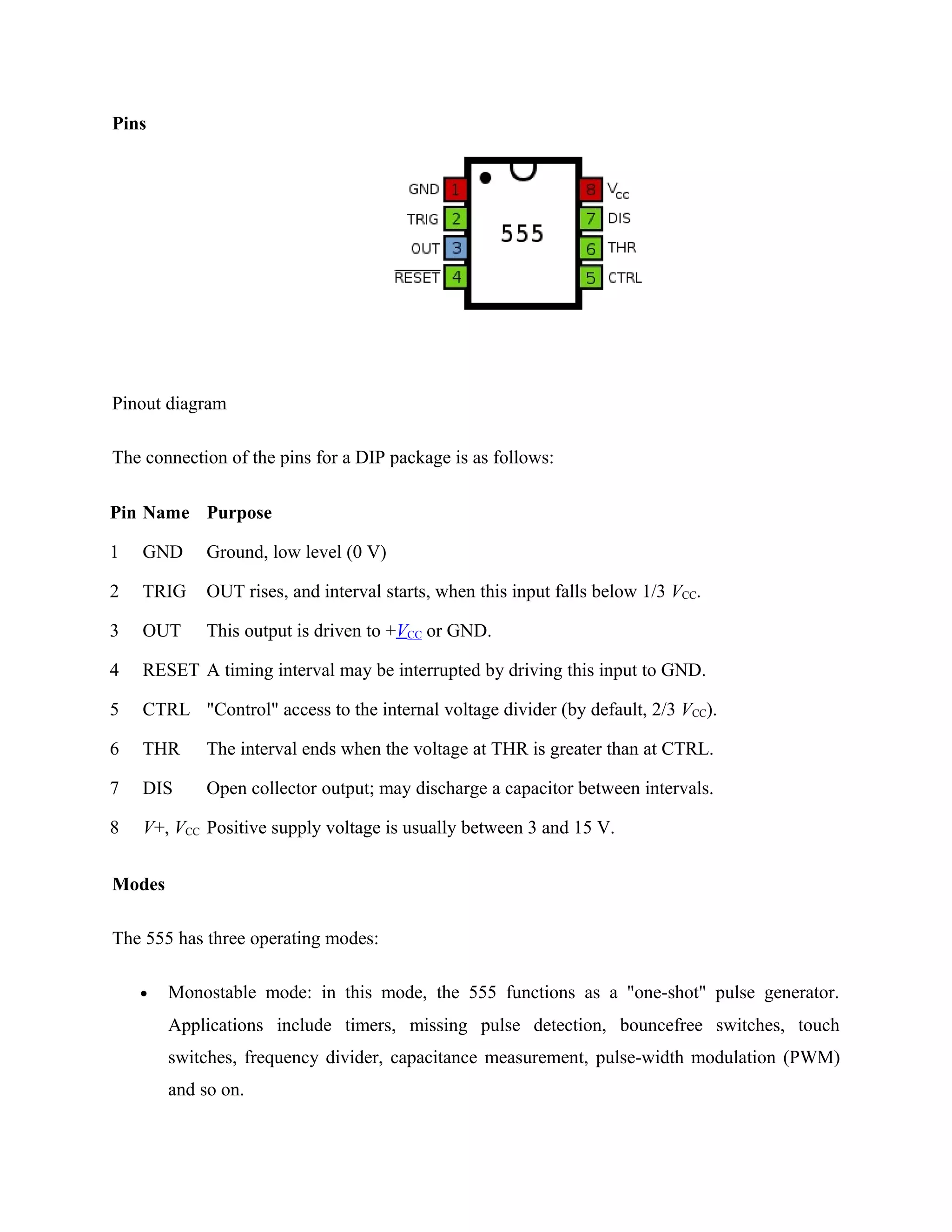

![In the monostable mode, the 555 timer acts as a “one-shot” pulse generator. The pulse begins
when the 555 timer receives a signal at the trigger input that falls below a third of the voltage
supply. The width of the output pulse is determined by the time constant of an RC network,
which consists of a capacitor (C) and a resistor (R). The output pulse ends when the voltage on
the capacitor equals 2/3 of the supply voltage. The output pulse width can be lengthened or
shortened to the need of the specific application by adjusting the values of R and C.[5]
The output pulse width of time t, which is the time it takes to charge C to 2/3 of the supply
voltage, is given by
where t is in seconds, R is in ohms and C is in farads. See RC circuit for an explanation of this
effect.
Bistable
In bistable mode, the 555 timer acts as a basic flip-flop. The trigger and reset inputs (pins 2 and 4
respectively on a 555) are held high via Pull-up resistors while the threshold input (pin 6) is
simply grounded. Thus configured, pulling the trigger momentarily to ground acts as a 'set' and
transitions the output pin (pin 3) to Vcc (high state). Pulling the reset input to ground acts as a
'reset' and transitions the output pin to ground (low state). No capacitors are required in a bistable
configuration. Pin 5 (control) is connected to ground via a small-value capacitor (usually 0.01 to
0.1 uF); pin 7 (discharge) is left floating.](https://image.slidesharecdn.com/555timer-170804145304/75/555-timer-4-2048.jpg)