Electronic Circuit Diode Wave Shaping
•
4 likes•4,365 views

1. The document discusses the principles of operation of p-n junction diodes and their use in analog electronic circuits. It describes how a diode only conducts current in one direction when forward biased and acts as an open switch when reverse biased. 2. Diode clipper circuits are introduced which can clip off portions of an input signal by only allowing the signal to pass through the diode when above or below a certain threshold set by a bias voltage. Parallel and series clipper configurations are examined along with their input-output characteristics. 3. Double-ended clipper circuits are described which can clip both the positive and negative portions of a signal simultaneously using two back-to-back diodes biased to conduct only

Recommended
More Related Content
What's hot
What's hot (20)
Viewers also liked
Viewers also liked (20)
Similar to Electronic Circuit Diode Wave Shaping
Similar to Electronic Circuit Diode Wave Shaping (20)
More from mohamed albanna
More from mohamed albanna (15)
Recently uploaded
Recently uploaded (20)
Electronic Circuit Diode Wave Shaping
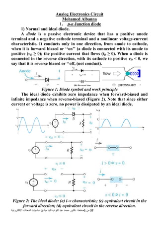
- 1. اﻻﻟﻜﺘﺮوﻧﻴﺔ اﻟﻤﻌﺪات اﺳﺎﺳﻴﺎت ﻣﺒﺎدئ اﻟﺒﻨﺎ اﻟﺘﻮاب ﻋﺒﺪ ﻣﺤﻤﺪ دآﺘﻮر 1ﺻﻔﺤﺔ ﻣﻦ 37 Analog Electronics Circuit Mohamed Albanna 1. p-n Junction diode 1) Normal and ideal diode. A diode is a passive electronic device that has a positive anode terminal and a negative cathode terminal and a nonlinear voltage-current characteristic. It conducts only in one direction, from anode to cathode, when it is forward biased or ‘‘on’’ (a diode is connected with its anode to positive (vD ≥ 0); the positive current that flows (iD ≥ 0). When a diode is connected in the reverse direction, with its cathode to positive vD < 0, we say that it is reverse biased or ‘‘off, (not conduct). Figure 1: Diode symbol and work principle The ideal diode exhibits zero impedance when forward-biased and infinite impedance when reverse-biased (Figure 2). Note that since either current or voltage is zero, no power is dissipated by an ideal diode. Figure 2: The ideal diode: (a) i–v characteristic; (c) equivalent circuit in the forward direction; (d) equivalent circuit in the reverse direction.
- 2. اﻻﻟﻜﺘﺮوﻧﻴﺔ اﻟﻤﻌﺪات اﺳﺎﺳﻴﺎت ﻣﺒﺎدئ اﻟﺒﻨﺎ اﻟﺘﻮاب ﻋﺒﺪ ﻣﺤﻤﺪ دآﺘﻮر 2ﺻﻔﺤﺔ ﻣﻦ 37 A practical application of diode Diode Wave Shaping There are two types of diode wave shaping circuits: clippers and clampers. Clipper: Separate an input signal at a particular dc level (clip off) and pass to the output, without distortion, the remaining upper or lower portion of the input waveform. This property can be used to limit the amplitude of a signal or to eliminate noise from an existing signal. A diode will not conduct until the forward bias voltage is at least as the forward break over voltage, (Ge diode 0.3V; Si diode 0.6V). For the ideal diode the transition between states will occur at Vd = 0 V and Id = 0 A. Applying the Id = 0 A at Vd = 0 V to the network of Figure 3 will result in the configuration of the next figure, where it is recognized that the level of vi that will cause a transition in state is For an input voltage greater than VB volts the diode is in the short-circuit state, while for input voltages less than VB volts it is in the open-circuit or “off” state. Figure 3: Determining the transition and Vo. When the diode is in the short-circuit state, the output voltage Vo can be determined by applying Kirchhoff’s voltage law in the clockwise direction Vi – VB – Vo = 0. 1- Parallel clipper Figure 4 shows a parallel clipper circuit with a 5 Vpp triangular input waveform. Figure 4: Parallel Clipper Circuit and waveforms During the positive half cycle, diode Cr1 is forward biased, the output voltage equals the forward voltage drop of the diode VF=0.7 V for Si diode. Any voltage greater than 0.7 V will shunt by diode Cr1, as a result, only a portion of the positive half cycle is passed through to the output. With diode Cr1 reverse biased, the entire input is passed through to the output.
- 3. اﻻﻟﻜﺘﺮوﻧﻴﺔ اﻟﻤﻌﺪات اﺳﺎﺳﻴﺎت ﻣﺒﺎدئ اﻟﺒﻨﺎ اﻟﺘﻮاب ﻋﺒﺪ ﻣﺤﻤﺪ دآﺘﻮر 3ﺻﻔﺤﺔ ﻣﻦ 37 By adding a dc voltage bias (battery) in series with the diode, the bias of the diode enables control over the portion of the input signal passed to the output. This effectively shifts the limiting point of the circuit. In each part of the figures, we can write Kirchhoff’s voltage law around the loop to determine the value of input voltage Vin that is necessary to forward bias the diode. Assuming that the diodes are ideal, we determine the value Vin necessary to forward bias each diode by determining the value Vin necessary to make VD > 0. When Vin reaches the voltage necessary to make VD > 0, the diode becomes forward biased and the signal source Vin is forced to, or held at, the dc voltage VB. If the forward voltage drop across the diode is not neglected, the clipping level is found by determining the value of Vin necessary to make VD greater than that forward drop (e.g., VD > 0.7 V for a Si diode). In positive clipping Since Vin = VD+ VB, then VD = Vin - VB, Since VD > 0 then Vin – VB > 0, and Vin > VB Figure 5 illustrates the concept of applying a 1 V bias to a parallel clipping circuit. Figure 5: Positive biased Positive parallel Clipper Circuit and waveforms During the positive half cycle, diode Cr1 is only forward biased when the input signal is greater than +1.7 V (Vin > VB +VCr1 > 1+ 0.7 > 1.7). Any portion of the input signal above +1.7 V will shunt by diode Cr1. When the input signal decreases below +1.7 V, diode Cr1 is reverse biased and the entire input signal is passed to the output. Figure 6 shows the clipping effect for a bias voltage of -2 V. Figure 6: Negative biased Positive parallel Clipper Circuit and waveforms Diode Cr1 will remain forward biased until the potential at the anode is (-2 + 0.7 = -1.3 V). As the input decreases below -1.3 V, (Vin < -VB + VCr1)
- 4. اﻻﻟﻜﺘﺮوﻧﻴﺔ اﻟﻤﻌﺪات اﺳﺎﺳﻴﺎت ﻣﺒﺎدئ اﻟﺒﻨﺎ اﻟﺘﻮاب ﻋﺒﺪ ﻣﺤﻤﺪ دآﺘﻮر 4ﺻﻔﺤﺔ ﻣﻦ 37 diode Cr1 will be reverse biased allowing the input waveform to pass through to the output. The limiting point of the circuit is now -1.3 V. In negative clipping Since Vin = VD - VB or VD = Vin + VB, Since VD > 0 then Vin + VB > 0, and Vin > - VB Figure 7 shows a negative parallel clipper circuit with a 4 V bias voltage. Figure 7: Positive biased Negative parallel Clipper Circuit and waveforms The negative half cycle has been clipped off in the output waveform. Diode Cr1 remains in the forward biased condition until the input signal increases above 3.3 V (Vin > VB - VCr1). The limiting point of the circuit is set at 3.3 V. Determine what value and polarity of total voltage Vin across the combination is necessary to forward bias the diode. Figure 8: Negative biased Negative parallel Clipper Circuit and waveforms Double-ended limiting circuits: Both positive and negative peaks of the output waveform are clipped. No more than one diode is forward biased at any given time and that both diodes are reverse biased for –E1 < vo < E2, the linear region. Figure 9 Double-ended clipping, If VB1 = 5 V, VCr1 = 0.7 V, then clip at 5.7 V if VB2 = 5 V, VCr2 = 0.7 V, then clip at and -5.7 V
- 5. وﻧﻴﺔ di as di اﻻﻟﻜﺘﺮو ﻤﻌﺪات 2- Se 1) N The iode in r Whe s open sw The iode in fo Outp اﻟﻤ اﺳﺎﺳﻴﺎت ئ eries clip egative b diode is reverse b en Vin< V witch. Th diode is forward put wave ﻣﺒﺎد اﻟﺒﻨﺎ ﻟﺘﻮاب pper biased p s reverse bias acts Vdc diode herefore s forwar bias acts eform اﻟ ﻋﺒﺪ ﻣﺤﻤﺪ ﻮر positive c e biased as open e is rever e, Vo= 0 V rd biased s as close دآﺘﻮ 5ﺻﻔﺤﺔ clipper d during switch. rsed bias V. d during ed switc ﻣﻦ 37 g positive Therefo sed. The g negativ h. There e half cy ore, Vo = e diode in ve half c efore, Vo ycle of i 0 V. n revers cycle of i o = -Vin + nput. Th e bias ac input. Th + Vdc. he cts he
- 6. وﻧﻴﺔ bi ac ac اﻻﻟﻜﺘﺮو ﻤﻌﺪات 2) po Whe ias acts a Whe cts as op The cts as clo Outp اﻟﻤ اﺳﺎﺳﻴﺎت ئ ositive b en Vin< V as closed en Vin > pen switc diode i osed swit put wave ﻣﺒﺎد اﻟﺒﻨﺎ ﻟﺘﻮاب iased po Vdc, the d switch. Vdc, the ch. There s forwa tch in fo eform اﻟ ﻋﺒﺪ ﻣﺤﻤﺪ ﻮر ositive cli diode i . Therefo diode is efore, Vo rd biase rward b دآﺘﻮ 6ﺻﻔﺤﺔ ipper is forwa ore, Vo= reverse o = 0 V ed durin bias. Vo= ﻣﻦ 37 rd biase Vdc - Vin biased. ng negat Vin ed. The n. Vo will The dio ive half diode in l have (-) ode in re f cycle. T n forwar ) value. everse bi The diod rd ias de
- 7. وﻧﻴﺔ ac bi di اﻻﻟﻜﺘﺮو ﻤﻌﺪات 3) N Whe cts as op Whe ias acts a The iode in r Outp اﻟﻤ اﺳﺎﺳﻴﺎت ئ egative b en Vin< V pen switc en Vin > as closed diode is reverse b put wave ﻣﺒﺎد اﻟﺒﻨﺎ ﻟﺘﻮاب biased n Vdc, the d ch. There Vdc, the d switch. s reverse bias acts eform اﻟ ﻋﺒﺪ ﻣﺤﻤﺪ ﻮر negative c diode is efore, Vo e diode i . Therefo e biased as open دآﺘﻮ 7ﺻﻔﺤﺔ clipper reverse o = 0 V is forwa ore, Vo = d during switch. ﻣﻦ 37 biased. ard biase = Vin – Vd negativ Therefo The dio ed. The Vdc ve half cy ore, Vo = ode in re diode in ycle of i 0 V everse bi n forwar input. Th ias rd he
- 8. وﻧﻴﺔ di bi ac اﻻﻟﻜﺘﺮو ﻤﻌﺪات 4) Po The iode in fo Whe ias acts a Vo = Whe cts as op Outp اﻟﻤ اﺳﺎﺳﻴﺎت ئ ositive b diode is forward en |Vin| < as closed Vdc – |V en |Vin|> pen switc put wave ﻣﺒﺎد اﻟﺒﻨﺎ ﻟﺘﻮاب biased ne s forwar bias acts < Vdc, th d switch Vin| >Vdc, the ch. There eform اﻟ ﻋﺒﺪ ﻣﺤﻤﺪ ﻮر egative c rd biased s as close he diode or short diode i efore, Vo دآﺘﻮ 8ﺻﻔﺤﺔ lipper d during ed switc is forwa t circuit. s revers o = 0 V ﻣﻦ 37 g positiv h. There ard bias . Therefo (since V se biased ve half cy efore, Vo sed. The ore, Vdc>Vin) d. The d ycle of i o = Vin + diode in diode rev input. Th Vdc n forwar verse bi he rd ias
- 9. اﻻﻟﻜﺘﺮوﻧﻴﺔ اﻟﻤﻌﺪات اﺳﺎﺳﻴﺎت ﻣﺒﺎدئ اﻟﺒﻨﺎ اﻟﺘﻮاب ﻋﺒﺪ ﻣﺤﻤﺪ دآﺘﻮر 9ﺻﻔﺤﺔ ﻣﻦ 37 The clipping takes place during the positive cycle only when the input voltage is greater than battery voltage (i.e. Vin > VB). The clipping level can be shifted up or down by varying the bias voltage (VB). Figure 10-a. Series with positive bias Clipping take place during the negative half cycle only when the input voltage Vin > VB. The clipping level can be shifted up or down by varying the voltage (-VB). Figure 10-b. Series with negative bias For these circuits, the direction of the diode suggests that the signal must be positive to turn it on. The dc supply further requires that the voltage be greater than VB volts to turn the diode on. The negative region of the input signal is “pressuring” the diode into the “off” state, supported further by the dc supply. In general, therefore, we can be quite sure that the diode is an open circuit (“off” state) for the negative region of the input signal. Example 1. Figure 11 shows a negative series clipper circuit with negative dc bias of 5 V. Note that with the biasing voltage VB in series with the input voltage, the resulting output signal has shifted in the dc level. Figure 11: Negative Series Clipper with dc Bias
- 10. اﻻﻟﻜﺘﺮوﻧﻴﺔ اﻟﻤﻌﺪات اﺳﺎﺳﻴﺎت ﻣﺒﺎدئ اﻟﺒﻨﺎ اﻟﺘﻮاب ﻋﺒﺪ ﻣﺤﻤﺪ دآﺘﻮر 01ﺻﻔﺤﺔ ﻣﻦ 37 For example, in Figure 11 when the input voltage is +10 V, the voltage at the anode of Cr1 is +15 V. This is because the biasing voltage VB is summed with the input waveform voltage. Subtracting the forward voltage drop of Cr1, results in a peak output voltage of 15 - 0.7 = +14.3 V. When the anode voltage of Cr1 falls below 0.7 V, Cr1 is reverse biased and the output voltage will be zero. This occurs when the input voltage decreases past (Vin - VB ) 0.7 – 5 = -4.3 V. A result of the biasing voltage being in series with the input signal is a dc voltage shift of 5 V at the anode of Cr1 over the entire positive and negative half cycles of the input. The forward voltage drop of the Cr1 results in a 4.3 V shifts at the output. By reversing the orientation of the diode in a series clipper circuit, the positive half cycle can be clipped from the input signal. This circuit is called a positive series clipper. Example 2. Figure 12 shows a positive series clipper circuit with a 5 V bias. Figure 12: Positive Series Clipper with dc Bias Note that Cr1 remains reverse biased until the input signal decreases below (-10 + 5 - 0.7) -5.7 V. Therefore only the portion of the signal less than -5.7 V will be passed through Cr1 to the output. Example 3: Figure 13 shows a positive clipping circuit, which removes any portion of the input signal vi that is greater than Vb and passes as the output signal vo any portion of vi that is less than Vb. Figure 13 As you can see, vD is negative when vi < Vb, causing the ideal diode to act as an open circuit. With no path for current to flow through R, the
- 11. اﻻﻟﻜﺘﺮوﻧﻴﺔ اﻟﻤﻌﺪات اﺳﺎﺳﻴﺎت ﻣﺒﺎدئ اﻟﺒﻨﺎ اﻟﺘﻮاب ﻋﺒﺪ ﻣﺤﻤﺪ دآﺘﻮر 11ﺻﻔﺤﺔ ﻣﻦ 37 value of vi appears at the output terminals as vo. However, when vi ≥ Vb, the diode conducts, acting as a short circuit and forcing vo=Vb. The diode blocks for vi < 6V and conducts for vi ≥ 6V. Thus, vo = vi for vi < 6V, and vo = 6V for vi ≥ 6V. Example 4: In the positive clipping circuit of Figure 13, the diode is ideal and vi is a 10 V triangular wave with period T. Sketch one cycle of the output voltage vo if Vb = 6V. The diode blocks (acts as an open circuit) for vi < 6V, giving vo = vi. For vi ≥ 6V, the diode is in forward conduction, clipping vi to effect vo = 6V. The resulting output voltage waveform is sketched in Figure 14. Figure 14 Example 5: Reverse the diode in Figure 13 to create a negative clipping network. (a) Let Vb = 6V, Sketch one cycle of the output waveform if vS = 10 sinωt V. (a) The diode conducts for vi ≤ 6 V and blocks for vi > 6V. Consequently, vo = vi for vi > 6 V, and vo = 6 V for vi ≤ 6 V. (b) With negative clipping, the output is made up of the positive peaks of 10 sinωt above 6V and is 6V otherwise. Figure 18 displays the output waveform. Figure 18
- 12. اﻻﻟﻜﺘﺮوﻧﻴﺔ اﻟﻤﻌﺪات اﺳﺎﺳﻴﺎت ﻣﺒﺎدئ اﻟﺒﻨﺎ اﻟﺘﻮاب ﻋﺒﺪ ﻣﺤﻤﺪ دآﺘﻮر 21ﺻﻔﺤﺔ ﻣﻦ 37 Clamping A circuit that places either the positive or negative peak of a signal at a desired dc level is known as a clamping. A clamping adds a dc component to the signal and does not change the shape or amplitude of the input signal. Clamping circuits consist of a capacitor, a diode and a resistor. An independent dc biasing voltage can also be employed to provide an additional voltage shift. For clamping circuits, the total swing in the output is equal to the total swing of the input. Only the dc reference level has changed. Adding a dc bias to a clamping circuit will provide additional shift in the dc reference level of the output. When a signal drives an open-ended capacitor the average voltage level on the output terminal of the capacitor is determined by the initial charge on that terminal and may therefore be quite unpredictable. Thus it is necessary to connect the output to ground or some other reference voltage via a large resistor. This action drains any excess charge and results in an average or dc output voltage of zero. A simple alternative method of establishing a dc reference for the output voltage is by using a diode clamp as shown in figure 19. By conducting whenever the voltage at the output terminal of the capacitor goes negative, this circuit builds up an average charge on the terminal that is sufficient to prevent the output from ever going negative. Positive charge on this terminal is effectively trapped." Figure 19 The steps involved in analyzing clamper circuits are: • always determine the forward biasing cycle first, • treat the diodes initially as ideal diodes and • Adjust the ideal voltage output for the practical diode forward voltage drop. 1- Positive Clamper Clamper circuit simply consists of a diode D and capacitor C as shown in below Figure. During the negative half cycle of the input voltage Vin the diode is forward biased and the current flows through the circuit. As a result of this, the capacitor C is charged to a voltage equal to the negative peak value i.e., -Vm. Once the capacitor is fully charged to -Vm it cannot
- 13. وﻧﻴﺔ di m T T th be ca bi co m du ac vo = co ca tim cy th re T re اﻻﻟﻜﺘﺮو ﻤﻌﺪات ischarge means tha he pola herefore he capaci 2- N If we ecomes n To p apacitor iased re onstant a Whe must be uring th chieved b The olts. For 0 V). Duri onductin ase 10 V me cons ycle will his equal Duri emains f he capa esulting اﻟﻤ اﺳﺎﺳﻴﺎت ئ e becaus at this c rity of e the out itor volt Negative C e change negative produce C1 must esistor R and allow en Cr1 is large en he period by the co circuit s r the ana ing the ng, capac V). Capac tant pro be equa ls zero vo ing the fully cha acitor's - output ﻣﺒﺎد اﻟﺒﻨﺎ ﻟﺘﻮاب e the di capacitor this vol tput volt tage Vm Clamper e the pol clamper good cla t be very R1 is by ws C1 to s reverse nough t d that C ombinat shown in alysis of Figure 2 positive citor C1 citor C1 oduced b al to the olts. negative arged be -10 V is voltage اﻟ ﻋﺒﺪ ﻣﺤﻤﺪ ﻮر iode can r acts as ltage is tage is eq i.e., Vin r larity of r. amping o y small. T ypassed. charge v e biased to ensur Cr1 is rev tion of R n Figure this circ 20, Clam e half c will cha will cha by Cr1. T forward e half cy ecause o combin will be دآﺘﻮ 31ﺻﻔﺤﺔ nnot con s a batte such th qual to t + Vm. f the dio of the in This is a This re very qui d, the ma re that c verse bia R1 and C1 20 will c cuit, assu mping Cir cycle, C arge up arge up The volta d voltage ycle Cr1 f the lon ned with e twice 3 ﻣﻦ 37 nduct in ery with hat it a the sum de and c nput wav achieved esults in ickly. agnitude capacito ased. A l 1. clamp th ume that rcuit Wa Cr1 is fo to the p very qui age outpu e drop o 1 is reve ng time h the -10 the neg the rev an emf adds to of the a capacito veform, t by Cr1. n a very e of the or C1 do large RC he input t Cr1 is a aveforms orward b peak inp ickly be ut durin of Cr1. F erse bias constan 0 V inp ative vo verse dir equal to the inp c input s or, then t the char With Cr y small RC time oes not C time c wavefor an ideal s biased. ut volta cause of ng the po For the id sed. Cap t formed ut signa oltage in rection. o the -Vm put signa signal an the circu rge time r1 forwar RC tim e consta dischar constant rm to ze diode (V With C ge (in th f the sho ositive ha deal diod pacitor d with R al and th nput. It It Vm. al. nd uit of rd me ant ge is ro VF Cr1 his ort alf de C1 R1. he is
- 14. اﻻﻟﻜﺘﺮوﻧﻴﺔ اﻟﻤﻌﺪات اﺳﺎﺳﻴﺎت ﻣﺒﺎدئ اﻟﺒﻨﺎ اﻟﺘﻮاب ﻋﺒﺪ ﻣﺤﻤﺪ دآﺘﻮر 41ﺻﻔﺤﺔ ﻣﻦ 37 important to note that the capacitor acts essentially as a battery in series with the input. In analyzing clamper circuits with bias, it is easier to first examine the cycle in which the diode is forward biased. For the circuit shown in Figure 21, diode Cr1 is forward biased in the negative half cycle of the input signal. Figure 21. Clamping Circuit and Waveforms As Cr1 is an ideal diode, when the input voltage decreases to -4 V, it will conduct. This will charge C1 to a voltage of -6 V (the remaining voltage of the input signal). The output voltage is equal to the biasing voltage of VB (-4V). Examining the positive half cycle, diode Cr1 is reverse biased. The 6V charge stored in capacitor C1 is summed with the input voltage. The resulting output voltage is therefore +16 V. Note that the voltage swing is still 20 V; only the reference level has changed. If the diode in Figure 21 was a silicon diode, the forward voltage drop would have to be taken into account. The voltage output waveform for a silicon diode would have the positive half cycle clamped to +15.3 V and the negative half cycle clamped to -4.7 V. Figure 22 illustrates a summary of the configurations and expected outputs for clamper circuits. Figure 22. Clamping Circuits
- 15. اﻻﻟﻜﺘﺮوﻧﻴﺔ اﻟﻤﻌﺪات اﺳﺎﺳﻴﺎت ﻣﺒﺎدئ اﻟﺒﻨﺎ اﻟﺘﻮاب ﻋﺒﺪ ﻣﺤﻤﺪ دآﺘﻮر 51ﺻﻔﺤﺔ ﻣﻦ 37 Voltage regulation (Zener diode) Voltage regulation is the measure of circuit ability to maintain a constant output even when input voltage or load current varies. When forward-biased, Zener diodes behave much the same as standard rectifying diodes. In reverse-bias mode, they do not conduct until the applied voltage reaches or exceeds the so-called Zener voltage, at which point the diode is able to conduct substantial current, and in doing so will try to limit the voltage dropped across it to that Zener voltage point. Figure 1. Zener diode characteristics Zener and Avalanche Diodes Zener diodes (ZD) and avalanche diodes are pn-diodes specially built to operate in reverse breakdown. Avalanche and Zener diodes are used as voltage regulators and as overvoltage protection devices. TC of Zener diodes is negative at VZ ≤ 3.5 to 4.5 V and is equal to zero at about VZ ≈ 5 V. TC of a Zener diode operating above 5 V is in general positive. Above 10 V the pn-diodes operate as avalanche diodes with a strong positive temperature coefficient. The motivation for using a Zener diode rather than a regular diode is the high voltage switching applications. While a regular diode provides switching behavior, the voltage involved is fairly small. With Zerner diode, voltage switching occurs on the order of magnitude of 100 V. Moreover, a very small change in the voltage induces a large change in current; therefore, the resistance is very small by Ohm’s Law, as the slope of the Zener diode characteristic is fairly large. The behavior will be described by two effects. 1. Zener effect: Increasing the reverse current VS causes an increase of the electric field in the depletion zone. The position of the valence band and of the conducting band will be relatively shifted in the energy band model. If the upper part of the valence band in the p-type is lying energetically higher than the lower part of the conducting band in the n- type, then electrons from the valence band in the p-type may tunnel
- 16. اﻻﻟﻜﺘﺮوﻧﻴﺔ اﻟﻤﻌﺪات اﺳﺎﺳﻴﺎت ﻣﺒﺎدئ اﻟﺒﻨﺎ اﻟﺘﻮاب ﻋﺒﺪ ﻣﺤﻤﺪ دآﺘﻮر 61ﺻﻔﺤﺔ ﻣﻦ 37 through the now very small forbidden energy gap into the conduction band in the n-type where they will be accelerated toward the positive pole. Fig. 2: Zener effect in the energy band model. 2. Avalanche effect: Increasing the reverse voltage VS causes an increase of the kinetic energies of electrons, which are responsible for the reverse current IS. If the energy of the electrons is sufficiently large, then these can release bound electrons of the valence band and may reach the conduction band, where they will be accelerated toward the positive pole. Then these electrons, which are already present in the conduction band, will gain kinetic energy, which is high enough to release further electrons from the valence or conduction band (avalanche effect). The size of the breakdown voltage depends on doping. In an ordinary diode the breakdown voltage is between 50 Volts and more than 1000 Volts. A Zener diode is highly doped such that the breakdown voltage is below 5 V depending on the amount of doping. Z-diodes are often used for stabilizing voltages, where the current can steeply increased by a slight varying voltage at the so called breakdown point. Z-diodes are used in power supplies of almost all electric apparatuses, as safety diode in circuits and in order to limit voltages. Zener Diode Regulator Model In breakdown, the diode is modeled with a voltage source, VZ, and a series resistance, RZ. RZ models the slope of the I-V characteristic. Figure 3, basic zener diode regulator model Important considerations: 1: Zener diode must remain in the breakdown region.
- 17. وﻧﻴﺔ di its ex ra en de ca vo in ap اﻻﻟﻜﺘﺮو ﻤﻌﺪات 2: P iode. VZm iR = 1: Vz Ri ≤ 2: Vp Ri ≥ From (mI V Z P IZ (m Solv (mIZ re% %reg s functio Con Whe xtremely ated curr nsure the Let's etermini alculatio oltage of The n this exa pproxim اﻟﻤ اﺳﺎﺳﻴﺎت ئ ower dis max IZmax LZ ZPS II VV + − Vz > Vzo ; (min)I (mV Z PS + Vps ≤ ratte (max)I (mV Z PS m the pr (Imin) (min) L PS + − min) = 0.1 ving (1) a I max) Z = egulation gulation on. nection en a Zen y close t rent (IZ) e consta s exami ing all v ons assum f 45 volts power s ample), t mately 12 ﻣﺒﺎد اﻟﺒﻨﺎ ﻟﺘﻮاب ssipated ≤ zener Z V IOr = Vps = m (maxI) Vmin) L Z + − ed diode (minI) Vmax) L Z + − revious e I(max) V Z Z = 1 IZ (max and (2) th [ V V(max) P PZ V (maV n L L = is used of Zener ner diod to the b ) to 10 pe ncy of vZ ine a z voltages, ming a z s, and a supply vo the volta 2.6 volts. اﻟ ﻋﺒﺪ ﻣﺤﻤﺪ ﻮر by zene r dissipat i ZPS R VV − − min; IZ = x) dissipati n) equation (max) (maxV Z PS + x) (2) hen (min)V (max)V PS PS − − )nom(V (mVax) L L− to meas r diode f de is in breakdow ercent or Z. zener di current zener vo series re oltage re age drop دآﺘﻮ 71ﺻﻔﺤﺔ er diode tion rati LI− min; IL tion; Vps s: (min)I Vx) Z Z− ] 0V9.0 IV Z ZZ −− −− 100 min) × sure how for volta reverse wn valu r less of iode reg ts, and p oltage VZ esistor va emains a pped acr 7 ﻣﻦ 37 e must n ing. = max = max IZ )1( [ (mV1.0 V(min) PS PZ 0 w well th ge regul breakd e while rated cu gulating power di Zener of 1 alue of 1 above the ross the z not excee Z = max; max) (min)VPS − he regula lation. down, its the cur urrent, s g circuit issipatio 12.6 volt 1000 Ω: e zener v zener dio ed rated ; IL = min ]VZ− ator is p s voltag rrent va so that iZ t mathe ns. We'l ts, a pow voltage ( ode will d value f n erformin e remai aries fro Z ≥ 0.1IZ ematicall ll perfor wer supp (12.6 vol remain for ng ns om to ly, rm ply lts, at
- 18. وﻧﻴﺔ vo vo m ca qu kΩ vo m co اﻻﻟﻜﺘﺮو ﻤﻌﺪات If th oltage is olts - 12. mA of cur Pow an calcu uite easil Presis Presis Pdiode Pdiode Take Ω resisto oltage ar With mA), both Presis Presis Pdiode Pdiode Con onnected If 12 اﻟﻤ اﺳﺎﺳﻴﺎت ئ he zener 45 volts .6 volts = rrent in wer is cal late pow ly: stor = (32. stor = 1.04 de = (32.4 de = 408.2 e this cir or. Note re identi h only 1/ h power stor = (324 stor = 10.4 de = (324µ de = 4.082 sider ou d in para 2.6 volts ﻣﺒﺎد اﻟﺒﻨﺎ ﻟﺘﻮاب r diode' s, there = 32.4 vo the circu culated wer dissi .4 mA)(3 498 W 4 mA)(12 24 mW rcuit, fo that bot cal to th /100 of t dissipat 4µA)(32. 498 mW µA)(12.6 24 mW ur first allel with s is main اﻟ ﻋﺒﺪ ﻣﺤﻤﺪ ﻮر s voltag will be 3 olts). 32 uit. by mult ipations 32.4V) 2.6V) or examp th the po he last ex the curre ion figur .4V) 6V) regulato h the zen ntained دآﺘﻮ 81ﺻﻔﺤﺔ ge is 12. 32.4 volt .4 volts d tiplying c for both ple, with ower sup xample: ent we h res shou or circu ner diode across a 8 ﻣﻦ 37 .6 volts ts dropp dropped current h the res h a 100 k pply volt had befor uld be 10 uit, this e: a 500 Ω and th ped acro d across by volta sistor an kΩ resis tage and re (324 µ 0 times s time wi load, th e power ss the re 1000 Ω age (P = nd the ze stor inste d the dio µA inste smaller: ith a 50 he load r supply esistor (4 gives 32 IE), so w ener diod ead of a ode's zen ead of 32 : 00 Ω loa will dra y's 45 2.4 we de a 1 ner 2.4 ad aw
- 19. اﻻﻟﻜﺘﺮوﻧﻴﺔ اﻟﻤﻌﺪات اﺳﺎﺳﻴﺎت ﻣﺒﺎدئ اﻟﺒﻨﺎ اﻟﺘﻮاب ﻋﺒﺪ ﻣﺤﻤﺪ دآﺘﻮر 91ﺻﻔﺤﺔ ﻣﻦ 37 25.2 mA of current. In order for the 1 kΩ series "dropping" resistor to drop 32.4 volts (reducing the power supply's voltage of 45 volts down to 12.6 across the zener), it still must conduct 32.4 mA of current. This leaves 7.2 mA of current through the zener diode. Example: Find the voltage vZ across the Zener diode if iZ =10 mA and it is known that VZ =5.6 V, IZ =25 mA, and RZ =10 Ω. Since 0.1 IZ ≤ iZ ≤ IZ, operation is along the safe and predictable region of Zener operation. Consequently, vZ = VZ + iZRZ = 5.6 + (10*10-3 )(10) = 5.7V Problem The Zener diode regulator circuit shown in Figure 4 has an input voltage of that varies between 10 and 14 V, and a load resistance that varies between RL = 20 and 100 Ω. Assume a 5.6 V zener is used and assume IZ (min) = 0.1 IZ (max). Find the value of Ri required and the maximum rating of the diode. Figure 4 Zener diode regulator circuit Problem A Zener diode is connected in a voltage regulator circuit as shown in Figure 4. The Zener voltage is Vz = 10 V and the Zener resistance is assumed to be rz = 0. (a) Determine the value of Ri such that the Zener diode remains in the breakdown region if the load current varies from IL = 50 to 500 mA and the input voltage varies from VI = 15 to 20 V. Assume IZ (min) = 0.1 IZ (max). (b) Determine the power rating required for the Zener diode and the load resistance Problem The secondary voltage in the circuit shown in Figure 5 is vs = 12 sin(at) V. The Zener diode parameters Vz = 8 V at Iz = 100 mA and rz = 0.5 Ω. Let Vv = 0, Ri = 3Ω. Determine the percent of regulation for load currents between IL = 0.2 and 1 A. Find the C such that the ripple voltage is no larger than 0.8 V.
- 20. اﻻﻟﻜﺘﺮوﻧﻴﺔ اﻟﻤﻌﺪات اﺳﺎﺳﻴﺎت ﻣﺒﺎدئ اﻟﺒﻨﺎ اﻟﺘﻮاب ﻋﺒﺪ ﻣﺤﻤﺪ دآﺘﻮر 02ﺻﻔﺤﺔ ﻣﻦ 37 Figure 5 Power Supply: Most of the electronic device and circuits needs direct current (dc) to work. Batteries produce dc, but there is a limit to how much energy and how much voltage a battery can provide. The electricity from the utility company is alternating current (ac) with a frequency of 60 Hz. The energy from a wall outlet is practically unlimited, but it must be converted from ac to dc, to be suitable for electronic equipment. Most power supplies consist of several stages, always in the same order (Fig. 6). Fig. 6, Block diagram of a power supply. Sometimes a regulator is not needed. First, the ac encounters a transformer that steps the voltage either down or up, depending on the exact needs of the electronic circuits. Second, the ac is rectified, so that it becomes pulsating dc with a frequency of 60 Hz. This is almost always done by one or more semiconductor diodes. Third, the pulsating dc is filtered, or smoothed out, so that it becomes a continuous voltage having either positive or negative polarity with respect to ground. Finally, the dc voltage might need to be regulated. Some equipment is finicky, insisting on just the right amount of voltage all the time. Other devices can put up with some voltage changes. Power supplies that provide more than a few volts must have features that protect the user from receiving a dangerous electrical shock. All power supplies need fuses and/or circuit breakers to minimize the fire hazard in case the equipment shorts out. Rectification ("frequency shifting") Most rectifier diodes are made of silicon and are therefore known as silicon rectifiers. Two important features of a power-supply diode are, the
- 21. وﻧﻴﺔ av ra ra cu is T 20 ci bi pl gr gr cy w % m th de co in de re ac w pr اﻻﻟﻜﺘﺮو ﻤﻌﺪات verage f ating. Aver Whe ating of a urrent is Note often q he instan 0 times ircuitry. Peak The ias, volta lace. A g reater th reat eno ycle. Thi will “buck The In a % of the r much as 2 Figu he top h epend at The omponen nterest, a esirable emove by The ction of when the redicts n اﻟﻤ اﺳﺎﺳﻴﺎت ئ forward rage forw en desig at least 1 s 4.0 A, t e that Io quite diff ntaneous Io, dep k inverse PIV rat age that good pow han the p ugh, the is will d k” the fo half-wav half-wa rms ac in 2.8 times ure below alf of th t all on t rectified nt. Gen and the to mov y a low-p equival the recti input is no loop ﻣﺒﺎد اﻟﺒﻨﺎ ﻟﺘﻮاب current ward cu ning a p 1.5 times the rectif flows th ferent fr s forwar pending e voltage ting of a it can w wer supp peak vol e diodes degrade orward c ve rectif ve circu nput volt s the rms w shows he input he size o d signal nerally, i un-welc ve the r pass filte lent circ ifier und s positive current اﻟ ﻋﺒﺪ ﻣﺤﻤﺪ ﻮر (Io) rat rrent power su s the exp fier diod hrough t rom this rd curren on the e (PIV) a diode withstand ply has d tage of t in a sup the effic current. fier it, the av tage. Ho s ac inpu a half-w t voltage of the loa is now it is the comed a ripple to er. cuit mod der these e but les and the دآﺘﻮ 12ﺻﻔﺤﺔ ting and upply, it pected a des shoul he diode s. Also, nt is ano e nature is the in d ()ﻳﺼﻤﺪ diodes w the ac at pply wil ciency of verage o owever, t ut voltag wave rec e signal, ad resist a comb e dc par c compo o high f del can e condit ss than t e output 1 ﻣﻦ 37 d the pe t’s wise verage d ld be rat es. The c note tha other thi e of th nstantan without whose PI t the inpu ll condu f the sup output vo the PIV ge. ctifier cir and for or. bination rt of a r onent is frequenc be used ions. Du the pn tu t signal eak inve to use dc forwa ted at Io current d at Io is a ing, and e power neous in t avalanc V rating ut. If the uct for p pply; th oltage is across th rcuit. Th r an ide of an a rectified describ cies whe d to eval uring the urn-on v voltage erse volt diodes w ard curre =6.0 A o drawn b an avera can be 1 r-supply verse, o che (ﻧﻬﻴﺎر gs are sig e PIV ra art of th he revers approxi he diode he signal eal diode ac signal d signal ed as ri ere it is luate th e part of voltage, is there tage (PI with an ent. If th or more. by the loa age figur 15 or eve y filterin r revers )اﻻﻧ takin gnificant ating is n he rever se curre imately 4 e can be l is exact e does n l and a that is ipple. It easier e detaile f the wa the mod efore zer IV) Io his ad re. en ng se- ng tly not rse ent 45 as tly not dc of is to ed ve del ro.
- 22. وﻧﻴﺔ W pr th po un it ta th gr T ne ou th pe m a ci th in 2. ha se اﻻﻟﻜﺘﺮو ﻤﻌﺪات When th roportio The A m he ac cyc olarity. nchange positive One apped se he exact round. T hese two egative h ut of pha he cycle ( Fig In th ercent o much as 2 PIV rati The The ircuit. Th he rms ac nput volt .1 times t Elec alves of econdary اﻟﻤ اﺳﺎﺳﻴﺎت ئ he inpu onal to, o full-wav much bett cle. Supp Then yo ed, and fl e instead commo condary t middle This pro o waves half of th ase, the o (Fig. 7). gure 7 sc his recti f the rm 2.8 times ing of at bridge r output he avera c input v tage. Th the rms Sche ctrically, f the wa y for one ﻣﺒﺎد اﻟﺒﻨﺎ ﻟﺘﻮاب ut excee or about ve, cente ter schem pose you ou can flip the n d. This is on full-w y, as show e of the oduces o can be he cycle. output o chematic ifier cir ms ac inp s the rms t least 4.2 rectifier wavefor age dc ou voltage. erefore, ac input ematic di the br ave cycl e half of اﻟ ﻋﺒﺪ ﻣﺤﻤﺪ ﻮر eds this 0.6 V lo er-tap re me for c u want t allow th negative the prin wave cir wn in Fi e second out-of-ph individ . Becaus of the cir c diagram cuit, the put volta s input v 2 times t rm is ju utput vo The PIV each dio t voltage iagram o idge cir le; the f the cycl دآﺘﻮ 22ﺻﻔﺤﺔ s voltag wer than ctifier changing to conve he posit portion nciple be rcuit use ig. 7. Th dary win hase wa dually ha se the wa rcuit has m of a fu e averag age. The voltage. T the rms a ust like oltage in V across ode need e. of a full- rcuit use center-t le, and t 2 ﻣﻦ 37 ge, the n the sou g ac to d ert an ac tive half of the w ehind ful es a tra e center nding, i aves at t alf-wave aves are s positive ull-wave, ge dc ou e PIV ac Therefor ac input. that of the brid the diod ds to hav wave bri es the e tap circu the other output urce volt dc is to u c wave t f of the wave ups ll-wave r ansforme r tap, a w is conne the ends e rectifie 180 deg e pulses center-ta utput vo cross the re, the d . the full dge circu des is 1.4 ve a PIV idge rect entire se uit uses r side fo signal tage." use both to dc wit ac cycl ide-dow rectificat er with wire com ected to s of the ed, cuttin grees (ha for both ap rectif oltage is e diodes diodes sh l-wave, c uit is 90 4 times t V rating tifier. econdary s one si r the oth becom h halves th positi le to pa wn, makin tion. a cente ming out o commo e windin ng off th alf a cycl h halves fier. about 9 can be hould ha center-ta percent the rms of at lea y on bo de of th her half mes of ve ass ng er- of on ng. he le) of 90 as ve ap of ac ast oth he of
- 23. اﻻﻟﻜﺘﺮوﻧﻴﺔ اﻟﻤﻌﺪات اﺳﺎﺳﻴﺎت ﻣﺒﺎدئ اﻟﺒﻨﺎ اﻟﺘﻮاب ﻋﺒﺪ ﻣﺤﻤﺪ دآﺘﻮر 32ﺻﻔﺤﺔ ﻣﻦ 37 the cycle. For this reason, the bridge circuit makes more efficient use of the transformer. The diodes act to route the current from both halves of the ac wave through the load resistor in the same direction, and the voltage developed across the load resistor becomes the rectified output signal. The diode bridge is a commonly used circuit and is available as a four-terminal component in a number of different power and voltage ratings. Power supply filtering Electronic equipment doesn’t like the pulsating dc that comes straight from a rectifier. The ripple in the waveform must be smoothed out, so that pure, battery-like dc is supplied. The filter does this. The simplest filter is one or more large-value capacitors, connected in parallel with the rectifier output. Electrolytic capacitors are almost always used. They are polarized; they must be hooked up in the right direction. Typical values range in the hundreds or thousands of microfarads. A simple filter. The capacitor, C, should have a large capacitance. The more current drawn, the more capacitance is needed for good filtering. This is because the load resistance decreases as the current increases. The lower the load resistance, the faster the filter capacitors will discharge. Larger capacitances hold charge for a longer time with a given load. Filter capacitors work by “trying” to keep the dc voltage at its peak level (Fig. 8). This is easier to do with the output of a full-wave rectifier (shown at A) as compared with a half-wave circuit (at B). The remaining waveform bumps are the ripple. With a half-wave rectifier, this ripple has the same frequency as the ac, or 60 Hz. With a full-wave supply, the ripple is 120 Hz. The capacitor gets recharged twice as often with a full-wave rectifier, as compared with a half-wave rectifier. This is why the ripple is less severe, for a given capacitance, with full-wave circuits.
- 24. اﻻﻟﻜﺘﺮوﻧﻴﺔ اﻟﻤﻌﺪات اﺳﺎﺳﻴﺎت ﻣﺒﺎدئ اﻟﺒﻨﺎ اﻟﺘﻮاب ﻋﺒﺪ ﻣﺤﻤﺪ دآﺘﻮر 42ﺻﻔﺤﺔ ﻣﻦ 37 Figure 8 Filtered output for full-wave rectification (A) and half-wave rectification (B). The rectified wave is dc only in the sense that it does not change polarity. But it does not have constant value and has plenty of ripples i.e. small waves. It has to be smoothed out in order to obtain authentic direct current. This can be done by means of a low-pass filter, which is shown in Figure below. Full-wave bridge with RC filter. The full-wave bridge diodes prevent flow of current back out of capacitor. The capacitor is an energy storage element. The energy stored in a capacitor is 2 CU 2 1 E = . For C in F (farads) and U in V (Volts), E comes out in J (jouls) and J = Watt/sec. The capacitor value is chosen so that f/1Rload >> , where f is the ripple frequency. For power line sine wave it is 2*50 Hz = 100 Hz. It allows ensuring small ripples, by making the time constant for discharge much longer than the time between recharging (the capacitor is charging very quickly, while discharging is very slow). It is quite easy to calculate the approximate ripple voltage. Let us assume that the load current stays constant (it will, for small ripples). The load causes the capacitor to discharge somewhat between cycles. The capacitor will lose some voltage, let us say UΔ . In this case, we have: t C I U ΔΔ = , (from dt dU CI = ) Instead of tΔ we use f/1 or f2/1 respectively for half-wave rectification and for full-wave rectification. Finally we obtain approximate ripple voltage: For halve-wave fC I U load=Δ , for full-wave fC2 I U load=Δ . If one wanted to do exact calculation with no approximation, one would use the exact exponential formula.
- 25. اﻻﻟﻜﺘﺮوﻧﻴﺔ اﻟﻤﻌﺪات اﺳﺎﺳﻴﺎت ﻣﺒﺎدئ اﻟﺒﻨﺎ اﻟﺘﻮاب ﻋﺒﺪ ﻣﺤﻤﺪ دآﺘﻮر 52ﺻﻔﺤﺔ ﻣﻦ 37 2. Bipolar Junction Transistors (BJT) The Transistor as a Switch Both the npn and pnp type bipolar transistors can be made to operate as "ON/OFF" type solid state switches. The areas of operation for a transistor switch are known as the Saturation Region and the Cut-off Region. This means then that we can ignore the operating Q-point biasing and voltage circuitry required for amplification, and uses the transistor as a switch by driving it back and forth between its fully-OFF (cut-off) and fully-ON (saturation) regions. The pink shaded area at the bottom of the curves represents the "Cut-off" region while the blue area to the left represents the "Saturation" region of the transistor. Both these transistor regions are defined as: 1. Cut-off Region Here the operating conditions of the transistor are zero input base current (IB), zero output collector current (IC) and maximum collector voltage (VCE) which results in no current flowing through the device. Therefore the transistor is switched Fully-OFF. Cut-off Characteristics • The input and Base are grounded (0v) • Base-Emitter voltage VBE < 0.7v • Base-Emitter junction is reverse biased • Base-Collector junction is reverse biased • Transistor is "fully-OFF" (Cut-off region) • No Collector current flows (IC = 0) • VOUT = VCE = VCC = "1" • Transistor operates as an "open switch" Then we can define the "cut-off region" or "OFF mode" when using a bipolar transistor as a switch as being, both junctions reverse biased, VB < 0.7v and IC = 0. For a pnp transistor, the Emitter potential must be negative with respect to the Base. 2. Saturation Region
- 26. اﻻﻟﻜﺘﺮوﻧﻴﺔ اﻟﻤﻌﺪات اﺳﺎﺳﻴﺎت ﻣﺒﺎدئ اﻟﺒﻨﺎ اﻟﺘﻮاب ﻋﺒﺪ ﻣﺤﻤﺪ دآﺘﻮر 62ﺻﻔﺤﺔ ﻣﻦ 37 Here the transistor will be biased so that the maximum amount of base current is applied, resulting in maximum collector current resulting in the minimum collector emitter voltage drop which results in the depletion layer being as small as possible and maximum current flowing through the transistor. Therefore the transistor is switched "Fully-ON". Saturation Characteristics • The input and Base are connected to VCC • Base-Emitter voltage VBE > 0.7v • Base-Emitter junction is forward biased • Base-Collector junction is forward biased • Transistor is "fully-ON" ( saturation region ) • Max Collector current flows (IC = Vcc/RL) • VCE = 0 ( ideal saturation ) • VOUT = VCE = "0" • Transistor operates as a "closed switch" Then we can define the "saturation region" or "ON mode" when using a bipolar transistor as a switch as being, both junctions forward biased, VB > 0.7v and IC= Maximum. For a pnp transistor, the Emitter potential must be positive with respect to the Base. Then the transistor operates as a "single-pole single-throw" (SPST) solid state switch. With a zero signal applied to the Base of the transistor it turns "OFF" acting like an open switch and zero collector current flows. With a positive signal applied to the Base of the transistor it turns "ON" acting like a closed switch and maximum circuit current flows through the device. An example of an npn Transistor as a switch being used to operate a relay is given below. With inductive loads such as relays or solenoids a flywheel diode is placed across the load to dissipate the back EMF generated by the inductive load when the transistor switches "OFF" and so protect the transistor from damage. If the load is of a very high current or voltage nature, such as motors, heaters etc, then the load current can be controlled via a suitable relay as shown.
- 27. اﻻﻟﻜﺘﺮوﻧﻴﺔ اﻟﻤﻌﺪات اﺳﺎﺳﻴﺎت ﻣﺒﺎدئ اﻟﺒﻨﺎ اﻟﺘﻮاب ﻋﺒﺪ ﻣﺤﻤﺪ دآﺘﻮر 72ﺻﻔﺤﺔ ﻣﻦ 37 Basic npn Transistor Switching Circuit To operate the transistor as a switch the transistor needs to be turned either fully "OFF" (cut-off) or fully "ON" (saturated). An ideal transistor switch would have infinite circuit resistance between the Collector and Emitter when turned "fully-OFF" resulting in zero current flowing through it and zero resistance between the Collector and Emitter when turned "fully-ON", resulting in maximum current flow. In practice when the transistor is turned "OFF", small leakage currents flow through the transistor and when fully "ON" the device has a low resistance value causing a small saturation voltage (VCE) across it. Even though the transistor is not a perfect switch, in both the cut-off and saturation regions the power dissipated by the transistor is at its minimum. In order for the Base current to flow, the Base input terminal must be made more positive than the Emitter by increasing it above the 0.7 volts needed for a silicon device. By varying this Base-Emitter voltage VBE, the Base current is also altered and which in turn controls the amount of Collector current flowing through the transistor. When maximum Collector current flows the transistor is said to be saturated. The value of the Base resistor determines how much input voltage is required and corresponding Base current to switch the transistor fully "ON". Inside the transistor, the small base current joins with the collector current to become the emitter current (or the emitter current divides to become the base and collector currents). This is expressed as IE = IC + IB (1) Where IE = emitter current IC = collector current IB = base current
- 28. اﻻﻟﻜﺘﺮوﻧﻴﺔ اﻟﻤﻌﺪات اﺳﺎﺳﻴﺎت ﻣﺒﺎدئ اﻟﺒﻨﺎ اﻟﺘﻮاب ﻋﺒﺪ ﻣﺤﻤﺪ دآﺘﻮر 82ﺻﻔﺤﺔ ﻣﻦ 37 However, because the collector current is usually so much larger than the base current, a useful approximation is to consider the collector current to be equal to the emitter current: IE ~ IC (2) The transistor dissipates power anytime there is a current flowing through it and a voltage is across it, expressed as PD = IC VCE (3) Where PD = power dissipated by the transistor IC = collector current VCE = voltage between the collector and emitter Example 1: Using the transistor values of: β = 200, Ic = 4 mA and IB = 20 uA, find the value of the Base resistor (RB) required to switch the load fully "ON" when the input terminal voltage exceeds 2.5 V. . . The next lowest preferred value is: 82 kΩ, this guarantees the transistor switch is always saturated. Example 2 Using the same values, find the minimum Base current required to turn the transistor "fully-ON" (saturated) for a load that requires 200 mA of current when the input voltage is increased to 5.0 V. Also calculate the new value of RB. Transistor Base current: Transistor Base resistance: . . . The behavior of the transistor may be illustrated by a load line on the output characteristics of the transistor. A load line is a line whose current-voltage (I-V) plot represents a load resistance, where the load line cuts any of the IB lines.
- 29. اﻻﻟﻜﺘﺮوﻧﻴﺔ اﻟﻤﻌﺪات اﺳﺎﺳﻴﺎت ﻣﺒﺎدئ اﻟﺒﻨﺎ اﻟﺘﻮاب ﻋﺒﺪ ﻣﺤﻤﺪ دآﺘﻮر 92ﺻﻔﺤﺔ ﻣﻦ 37 Fig 1: Transistor input and output characteristics. If the collector current IC is plotted against the collector-to-emitter voltage VCE, a family of curves for various fixed values of VBE or IB results, as in Figure 1. These curves show that as VCE increases, IC rises very rapidly and then turns over as it is limited by IB. In the Common Emitter circuit, if IB were reduced to zero, then IC would also be zero (apart from a small leakage current ICE0). Hence there would be no voltage drop in either RC or RE, and practically all of VCC would appear across the transistor. That is, under cut-off conditions, VCE → VCC for IB = 0 (4) Conversely, if IB were large, IC would be very large, almost all of VCC would be dropped across RC + RE and B EC CC C Iearglfor RR V I + → (5) Actually, because the initial rise in IC for the transistor is not quite vertical, there is always a small saturation voltage VCES across the transistor under these conditions, where VCES means the voltage across the transistor in the common-emitter mode when saturated. In this saturated condition VCES ≈ 0.3 V for small silicon transistors.
- 30. اﻻﻟﻜﺘﺮوﻧﻴﺔ اﻟﻤﻌﺪات اﺳﺎﺳﻴﺎت ﻣﺒﺎدئ اﻟﺒﻨﺎ اﻟﺘﻮاب ﻋﺒﺪ ﻣﺤﻤﺪ دآﺘﻮر 03ﺻﻔﺤﺔ ﻣﻦ 37 Figure 2 universal bias arrangement Note that because the transistor is non-ohmic (that is, it does not obey Ohm’s law), the voltage across it may only be determined by using the (ohmic) voltage drop across the resistors RC and RE according to Equation (6). At the quiescent point this is: VQ = VCC – IQ (RC + RE) From the circuit of Fig. 2 a, )6()RR(IVV ECCCCCE +−= , which may be rewritten as )7()VV( RR 1 RR V RR V I CCCE ECEC CE EC CC C − + −= + − + + = Figure 3. An example of a BJT constant current source It is simple to plot the load line for the circuit in figure 3. The open- circuit voltage for the x-axis value of the load line is simple the voltage across CE when the transistor is removed from the circuit. This value is: VCE (Sat) indicate the maximum possible value of VCE in the circuit. Next we will calculate the short-circuit current for the y-axis value of the load line. This value is:
- 31. اﻻﻟﻜﺘﺮوﻧﻴﺔ اﻟﻤﻌﺪات اﺳﺎﺳﻴﺎت ﻣﺒﺎدئ اﻟﺒﻨﺎ اﻟﺘﻮاب ﻋﺒﺪ ﻣﺤﻤﺪ دآﺘﻮر 13ﺻﻔﺤﺔ ﻣﻦ 37 This is the straight-line equation to the dc load-line (compare y = mx + c), showing that its slope is –1/ (RC + RE) and that it crosses the IC axis at VCC / (RC + RE) as expected. The actual position of a point is determined by where this load line crosses the output characteristic in use, that is, by what value of VBE or IB is chosen. For example, the quiescent point for the transistor is where the load line crosses the output curve defined by VBE = VBEQ (or IB = IBQ) to give VCE = VQ and IC = IQ. When the value of collector resistor has been chosen, bias is applied by passing current into the base so that the collector voltage drops to the desired value of around 0.5 VCC where VCC is the supply voltage. For any bias system, the desired base current must be equal to: 0.5 VCC/RLhFE with VCC in volts, RL (the load) in kΩ, hFE as a ratio. The amplification of a transistor can be recognized with the so called current-control characteristic. The collector current IC is plotted with respect to IB we can see that a small base current causes a large collector current. Fig. 4: Linear amplification range of a transistor (current-control characteristic). Under the proper operating conditions, IC will be some multiple of IB; in other words, the transistor is a current amplifier. The forward current gain (hFE or β) is expressed as: Where hFE = forward current gain IC = collector current IB = base current Example 1 A power transistor with an hFE of 50 is operating with a load current (IC ) of 3 A. What is the base current?
- 32. اﻻﻟﻜﺘﺮوﻧﻴﺔ اﻟﻤﻌﺪات اﺳﺎﺳﻴﺎت ﻣﺒﺎدئ اﻟﺒﻨﺎ اﻟﺘﻮاب ﻋﺒﺪ ﻣﺤﻤﺪ دآﺘﻮر 23ﺻﻔﺤﺔ ﻣﻦ 37 Solution: Recall that a transistor is basically a current amplifier where the IC is hFE times larger than the base current (IB ). By rearranging Equation 8, we can solve for IB : Let us see how the voltage-divider bias helps us set a Q-point independent of β. The term “voltage-divider bias” comes from the voltage divider formed by R1 and R2 in figure 3. The voltage across R2 should forward bias the emitter diode, VBE is forward-biased and VCE is reverse- biased. If we Thevenize the circuit as shown below, we get the circuit shown in figure 5 below. Figure 5: Circuit of figure 3 Thevenized at the base terminal, KVL loop shown. Since the transistor is in active region, IC*IE = ICE. Then , We can write a loop equation as shown in figure 5: Now, hence, the equation above becomes: If we want to swamp out the effects of β, a good rule of thumb is: R4 is 100 times greater than Rth/ β. Thus we want: Rth ≤ 0.01*β*R4. Thus, in
- 33. اﻻﻟﻜﺘﺮوﻧﻴﺔ اﻟﻤﻌﺪات اﺳﺎﺳﻴﺎت ﻣﺒﺎدئ اﻟﺒﻨﺎ اﻟﺘﻮاب ﻋﺒﺪ ﻣﺤﻤﺪ دآﺘﻮر 33ﺻﻔﺤﺔ ﻣﻦ 37 our circuit: Rth = 250 Ω < 0.01*220*150 = 330 Ω. Notice that the BJT will provide an amplified constant ICE as long as the Rth condition holds. Method of creating the bias voltage Figure 6 is a voltage-divider circuit shows that resistors R1 and R2 create a base bias voltage of 0.8 V (ignoring any loading effects). Consulting the input curve of Figure 1, we see that 0.8 V would cause a base current IB of 2 mA. Notice the load line shows that if 0.1 mA ≤ IB < 0.2 mA, then the BJT is guaranteed to be in active region. Figure 6: A voltage-divider bias circuit. The hFE of the transistor is given as 100, so rearranging Equation 8 we can calculate the collector current: IC = hFE IB = 100*2 mA = 200 mA Notice that the load is in series with the collector so that all 200 mA is going through the transistor and the load. Now consider an input signal voltage of ±0.1 V, which is superimposed onto the base through a capacitor. In other words, the input is added to the 0.8 Vdc bias voltage to form an ac base voltage that cycles from 0.7 to 0.9 V, as shown in Figure 7. Referring again to the base curve (Figure 1), we see that a base voltage of 0.7-0.9 V translates into a base current of 1-3 mA, which the transistor multiplies into a collector current of 100-300 mA, and all of this current goes through the load.
- 34. اﻻﻟﻜﺘﺮوﻧﻴﺔ اﻟﻤﻌﺪات اﺳﺎﺳﻴﺎت ﻣﺒﺎدئ اﻟﺒﻨﺎ اﻟﺘﻮاب ﻋﺒﺪ ﻣﺤﻤﺪ دآﺘﻮر 43ﺻﻔﺤﺔ ﻣﻦ 37 Figure 7: A simple transistor amplifier. Notice that the output voltage VC is out of phase with the output current IC . This occurs because the transistor must lower its resistance to increase the current, and a lower resistance creates a lower voltage drop. When we add a sinusoidal source with amplitude of ΔVBB in series with VBB, in response to this additional source, the base current will become iB + ΔiB leading to the collector current of iC + ΔiC and CE voltage of VCE + ΔVCE. These changes are shown in figure 7. Example 2 Find the load current in the transistor circuit shown in Figure 8. Use the input curves in Figure 1 and assume that the hFE of the transistor is 70. Solution Figure 8: A transistor circuit We want to find the output current, and because we know the current gain is 70, the problem comes down to finding out what the base
- 35. اﻻﻟﻜﺘﺮوﻧﻴﺔ اﻟﻤﻌﺪات اﺳﺎﺳﻴﺎت ﻣﺒﺎدئ اﻟﺒﻨﺎ اﻟﺘﻮاب ﻋﺒﺪ ﻣﺤﻤﺪ دآﺘﻮر 53ﺻﻔﺤﺔ ﻣﻦ 37 current is. In most cases, such as this one, it is the base voltage that we can calculate (or measure), so we will use the input curves to find the corresponding base current. First, calculate the base bias voltage from R1 and R2 using the voltage-divider rule: . . Now, knowing that the base voltage is 0.77 V, we use the input curve of Figure 1 to determine that IB is about 1.7 mA. The load current IC can now be calculated by rearranging Equation 8: IC = hFE IB = 70*1.7 mA = 119 mA 3- Field-Effect Transistors FET Transfer Conductance The slope of the transfer curve, dIDS /dVGS, is the dynamic forward transfer conductance, or mutual transfer conductance, gm. We see that gm starts off at zero when VGS = VP and increases as IDS increases, reaching a maximum when IDS = IDSS. Since IDS = IDSS [1 – (VGS /VP)] 2 , gm can be obtained as P P GS DSS GS DS m V V V 1 I2 dV dI g ⎟⎟ ⎠ ⎞ ⎜⎜ ⎝ ⎛ − == (1) Since DSS DS P GS I I V V 1 =− we have that P DSSDS P DSSDS DSSm V I.I 2 V I/I I2g == The maximum value of gm is obtained when VGS = 0 (IDS = IDSS) and is given by gm (VGS = 0) = gm0 = 2IDS / (VP).
- 36. اﻻﻟﻜﺘﺮوﻧﻴﺔ اﻟﻤﻌﺪات اﺳﺎﺳﻴﺎت ﻣﺒﺎدئ اﻟﺒﻨﺎ اﻟﺘﻮاب ﻋﺒﺪ ﻣﺤﻤﺪ دآﺘﻮر 63ﺻﻔﺤﺔ ﻣﻦ 37 Figure 1: A metal oxide semiconductor field effect transistor Example 1 For the power MOSFET whose characteristic curves are shown in Figure 1 (b), find the gain gm. Solution From Equation 1, we see that the gain gm is the change in output current due to the corresponding change in input gate voltage. Thus, we pick two convenient gate voltages—say, 5 V and 6 V (which represents a change of 1 V) — and divide that into the corresponding change in the load current IDS : )mho1or(S1 V1 A1 )V5V6( )A1A2( V I g GS DS m == − − == Δ Δ Some important characteristics of Motorola MTW24N40E power MOSFET are as follows: 1. Maximum load current (IDS ) is 24 A. 2. The gate threshold voltage (VGS(th)), the gate voltage that just causes the FET to con- duct, is between 2 and 4 V. 3. the minimum FET gain, called the forward transconductance (gFS ), is 11 mho. (Note: gFS is the same as gm.) 4. Total power dissipation for the FET (PD ) should be less than 250 W. Example 2 A particular power FET (MTW24N40E) was found to just start conducting when VGS = 2.5 V. Also, when VGS = 3 V, the load current (ID ) was measured to be 6 A. Is this FET operating within specifications? Solution The spec sheet shows that the gate-threshold voltage VGS (th) can be between 2 V and 4 V. Thus if this FET starts conducting with a gate
- 37. اﻻﻟﻜﺘﺮوﻧﻴﺔ اﻟﻤﻌﺪات اﺳﺎﺳﻴﺎت ﻣﺒﺎدئ اﻟﺒﻨﺎ اﻟﺘﻮاب ﻋﺒﺪ ﻣﺤﻤﺪ دآﺘﻮر 73ﺻﻔﺤﺔ ﻣﻦ 37 voltage of 2.5 V, it meets this spec. The second set of data gives one operating point. Specifically, we are told that an input voltage (VGS = 3 V) gives a corresponding output current (ID = 6 A). These numbers allow us to calculate the gain (transconductance) 12 V5.0 A6 )V5.2V3( )A0A6( V I gg GS DS FSm == − − === Δ Δ The operating value of gFS = 12 is above the minimum spec sheet value of 11, so the FET is OK. EXERCISES 1. A transistor has a current gain of 60 and a collector current of 5 A. Find the base current. 2. A transistor has a current gain of 40 and a base current of 25 mA. Find the collector current. 3. Calculate the exact and approximate emitter currents for the transistor described in Exercise 12. 4. A transistor with a gain of 35 has an input curve similar to that shown in Figure. The base voltage (VBE ) is measured to be 0.8 V. a. Find the base current. b. Find the collector current. 5. For the transistor circuit shown in Figure, calculate IC if the resistor R1 is changed to 1.3 kΩ. (Assume input curve Figure applies.) 6. For the transistor circuit shown in Figure 4.19, calculate the IC if the resistor R2 is changed to 120 kΩ. (Assume input curve Figure applies.) 7. For the FET circuit shown in Figure, find the load current if the gate voltage is 6.5 V. 8. A circuit uses the MTW24N40E MOSFET (Figure) and has a gate voltage (VGS ) of 5 V. Find the minimum and maximum drain current that could be expected in this circuit. (Assume gm = 12 mho.)