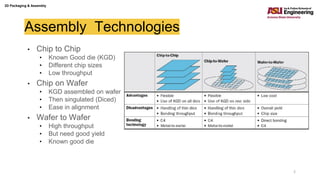
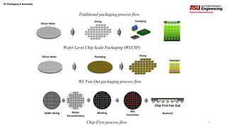
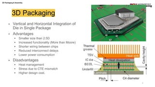
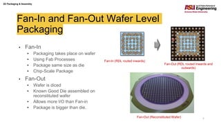
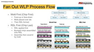
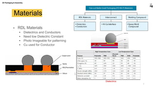
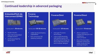
2D Packaging & Assembly
Packaging Process ​
2.8 Advanced Packaging
Levels 3 &4
2D Packaging & Assembly
Assembly Technologies
• Chip to Chip
• Known Good die (KGD)
• Different chip sizes
• Low throughput
• Chip on Wafer
• KGD assembled on wafer
• Then singulated (Diced)
• Ease in alignment
• Wafer to Wafer
• High throughput
• But need good yield
• Known good die
2
2D Packaging & Assembly
3
Traditional packaging process flow.
Wafer Level Chip Scale Packaging (WLCSP)
WL Fan-Out packaging process flow
Chip-First process flow
2D Packaging & Assembly
3D Packaging
• Vertical and Horizontal Integration of
Die in Single Package
• Advantages
• Smaller size than 2.5D
• Increased functionality (More than Moore)
• Shorter wiring between chips
• Reduced interconnect delays
• Lower power consumption
• Disadvantages
• Heat management
• Stress due to CTE mismatch
• Higher design cost.
4
2D Packaging & Assembly
Fan-In and Fan-Out Wafer Level
Packaging
• Fan-In
• Packaging takes place on wafer
• Using Fab Processes
• Package same size as die
• Chip-Scale Package
• Fan-Out
• Wafer is diced
• Known Good Die assembled on
reconstituted wafer
• Allows more I/O than Fan-in
• Package is bigger than die.
Fan-In (RDL routed inwards)
Fan-Out (RDL routed inwards and
outwards)
Fan-Out (Reconstituted Wafer) 5
2D Packaging & Assembly
Fan Out WLP Process Flow
• Mold First (Chip First)
• Face-up or face-down
• Mold placed over die
• Then RDL formed
• RDL First (Chip Last)
• RDL applied first
• Bumped chips assembled
onto RDL
• Assembly then coverrd
by mold
6
2D Packaging & Assembly
Materials
• RDL Materials
• Dielectrics and Conductors
• Need low Dielectric Constant
• Photo Imageable for patterning
• Cu used for Conductor
Dielectrics
7
2D Packaging & Assembly
WLP Packaging Tools
• Pick and Place
• Accurate placement required
• Compression Molding
• Transfer Molded – Wire-bonds, Flip-Chip
• Compression Molding – WLP
• Minimal Pressure
• Minimal tooling changes
• Challenge Die Shift
• Challenge Warpage
8
2D Packaging & Assembly
WLP Packaging
Tools
• Lithography
• Used to patter RDL wiring
• Needs to accommodate any warpage
• Physical Vapor Deposition
• Provides seed layers for Cu deposition
• Needs clean dry surface
• Electro-plating and bump formation
• Builds up copper layers
• Can be used for Cu Bumps
9
2D Packaging & Assembly
Challenges for FO WLP
• Die Shift
• Occurs during molding process
• Results in miss-alignment for RDLS
• Mold Shrinkage and warpage
• Need to optimize materials and process
• Board level reliability
• Very small stand-off height
10
2D Packaging & Assembly
11
Intel
2D Packaging & Assembly
12
Intel
2D Packaging & Assembly
13
TSMC CoWoS-S Nvidia H-100
https://www.semianalysis.com/p/ai-capacity-constraints-cowos-and
814 square millimeters
80 G memory
2D Packaging & Assembly
14
TSMC CoWoS-S Nvidia H-100
2D Packaging & Assembly
15
TSMC CoWoS-S
Nvidia H-100
NVIDIA DGX H100
2D Packaging & Assembly
16
TSMC CoWoS-S
Nvidia H-100

2.8 Advanced Packaging Levels 3 & 4.pdf

  • 1.
    2D Packaging &Assembly Packaging Process ​ 2.8 Advanced Packaging Levels 3 &4
  • 2.
    2D Packaging &Assembly Assembly Technologies • Chip to Chip • Known Good die (KGD) • Different chip sizes • Low throughput • Chip on Wafer • KGD assembled on wafer • Then singulated (Diced) • Ease in alignment • Wafer to Wafer • High throughput • But need good yield • Known good die 2
  • 3.
    2D Packaging &Assembly 3 Traditional packaging process flow. Wafer Level Chip Scale Packaging (WLCSP) WL Fan-Out packaging process flow Chip-First process flow
  • 4.
    2D Packaging &Assembly 3D Packaging • Vertical and Horizontal Integration of Die in Single Package • Advantages • Smaller size than 2.5D • Increased functionality (More than Moore) • Shorter wiring between chips • Reduced interconnect delays • Lower power consumption • Disadvantages • Heat management • Stress due to CTE mismatch • Higher design cost. 4
  • 5.
    2D Packaging &Assembly Fan-In and Fan-Out Wafer Level Packaging • Fan-In • Packaging takes place on wafer • Using Fab Processes • Package same size as die • Chip-Scale Package • Fan-Out • Wafer is diced • Known Good Die assembled on reconstituted wafer • Allows more I/O than Fan-in • Package is bigger than die. Fan-In (RDL routed inwards) Fan-Out (RDL routed inwards and outwards) Fan-Out (Reconstituted Wafer) 5
  • 6.
    2D Packaging &Assembly Fan Out WLP Process Flow • Mold First (Chip First) • Face-up or face-down • Mold placed over die • Then RDL formed • RDL First (Chip Last) • RDL applied first • Bumped chips assembled onto RDL • Assembly then coverrd by mold 6
  • 7.
    2D Packaging &Assembly Materials • RDL Materials • Dielectrics and Conductors • Need low Dielectric Constant • Photo Imageable for patterning • Cu used for Conductor Dielectrics 7
  • 8.
    2D Packaging &Assembly WLP Packaging Tools • Pick and Place • Accurate placement required • Compression Molding • Transfer Molded – Wire-bonds, Flip-Chip • Compression Molding – WLP • Minimal Pressure • Minimal tooling changes • Challenge Die Shift • Challenge Warpage 8
  • 9.
    2D Packaging &Assembly WLP Packaging Tools • Lithography • Used to patter RDL wiring • Needs to accommodate any warpage • Physical Vapor Deposition • Provides seed layers for Cu deposition • Needs clean dry surface • Electro-plating and bump formation • Builds up copper layers • Can be used for Cu Bumps 9
  • 10.
    2D Packaging &Assembly Challenges for FO WLP • Die Shift • Occurs during molding process • Results in miss-alignment for RDLS • Mold Shrinkage and warpage • Need to optimize materials and process • Board level reliability • Very small stand-off height 10
  • 11.
    2D Packaging &Assembly 11 Intel
  • 12.
    2D Packaging &Assembly 12 Intel
  • 13.
    2D Packaging &Assembly 13 TSMC CoWoS-S Nvidia H-100 https://www.semianalysis.com/p/ai-capacity-constraints-cowos-and 814 square millimeters 80 G memory
  • 14.
    2D Packaging &Assembly 14 TSMC CoWoS-S Nvidia H-100
  • 15.
    2D Packaging &Assembly 15 TSMC CoWoS-S Nvidia H-100 NVIDIA DGX H100
  • 16.
    2D Packaging &Assembly 16 TSMC CoWoS-S Nvidia H-100