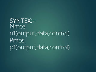
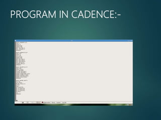
Download to read offline


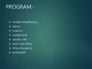
![MAIN PROGRAM DECODER:-
module decoder(a,b,i);
input a,b;
output [3:0]i;
wire abar,bbar;
notgate1 z1(a,abar);
notgate1 z2(b,bbar);
andgate z3(abar,bbar,i[0]);
andgate z4(abar,b,i[1]);
andgate z5(a,bbar,i[2]);
andgate z6(a,b,i[3]);
endmodule](https://image.slidesharecdn.com/2x4decoderusingswitchlevelaloksinghkanpur-180420191510/85/2-x4-decoder-using-switch-level-Alok-singh-kanpur-13-320.jpg)
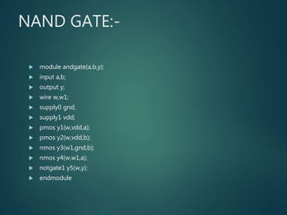
![TEST BENCH:-
module decoder_test();
reg a,b;
wire [3:0]i;
decoder d1(a,b,i);
initial
begin
a=1'b0;b=1'b0;
#5 a=1'b0;b=1'b1;
#5 a=1'b1;b=1'b0;
#5 a=1'b1;b=1'b1;
#5 $stop;
end
endmodule](https://image.slidesharecdn.com/2x4decoderusingswitchlevelaloksinghkanpur-180420191510/85/2-x4-decoder-using-switch-level-Alok-singh-kanpur-14-320.jpg)


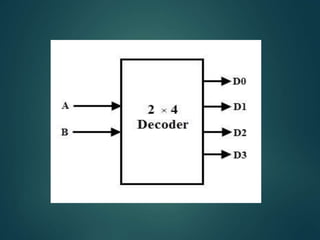
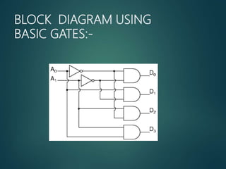
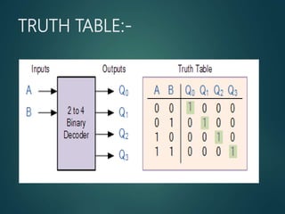
This document describes a student project to design a 2-to-4 decoder using switch level modeling in Verilog. It includes the student's name and registration details, an overview of switch level modeling, descriptions of basic logic gates like NOT, NAND using PMOS and NMOS transistors, the structure of a decoder, a block diagram and truth table for the decoder design, the Verilog code for the decoder module using basic gates, and a test bench module to simulate the decoder.