Download to read offline


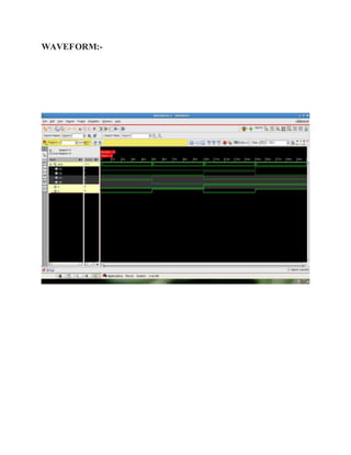
![PROGRAM:-
module notgate1(x,y);
input x;
output y;
supply0 gnd;
supply1 vdd;
pmos x1(y,vdd,x);
nmos x2(y,gnd,x);
endmodule
module andgate(a,b,y);
input a,b;
output y;
wire w,w1;
supply0 gnd;
supply1 vdd;
pmos y1(w,vdd,a);
pmos y2(w,vdd,b);
nmos y3(w1,gnd,b);
nmos y4(w,w1,a);
notgate1 y5(w,y);
endmodule
module decoder(a,b,i);
input a,b;
output [3:0]i;
wire abar,bbar;
notgate1 z1(a,abar);
notgate1 z2(b,bbar);
andgate z3(abar,bbar,i[0]);
andgate z4(abar,b,i[1]);
andgate z5(a,bbar,i[2]);
andgate z6(a,b,i[3]);
endmodule
module decoder_test();
reg a,b;
wire [3:0]i;
decoder d1(a,b,i);
initial
begin
a=1'b0;b=1'b0;
#5 a=1'b0;b=1'b1;
#5 a=1'b1;b=1'b0;
#5 a=1'b1;b=1'b1;
#5 $stop;
end
endmodule](https://image.slidesharecdn.com/switchlevelmodeling2x4-180420191711/85/Switch-level-modeling-2-x4-4-320.jpg)


The switch level modeling provides an abstraction between logic and transistor levels. It models transistors as either on or off, conducting or not conducting. Interconnect values are abstracted to a small number of discrete signal strengths. A binary decoder converts binary inputs to unique outputs, used for applications like data demultiplexing and memory address decoding. An example decoder is implemented using basic gates like NOT, NAND in a Verilog program and tested with a testbench that applies inputs over time.


![Lecture-5-[CCII].pdfmmmmmmmmmmmmmmmmmmmmmm](https://cdn.slidesharecdn.com/ss_thumbnails/lecture-5-ccii-251130051516-8d9b6959-thumbnail.jpg?width=640&height=640&fit=bounds)


