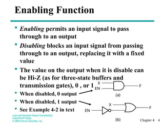
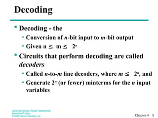
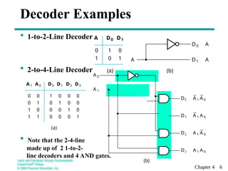
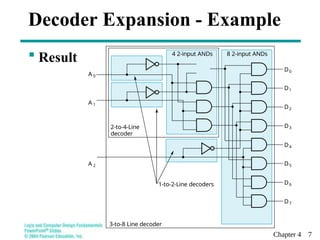
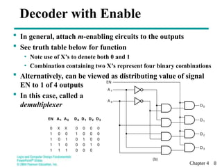
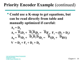
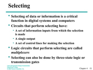
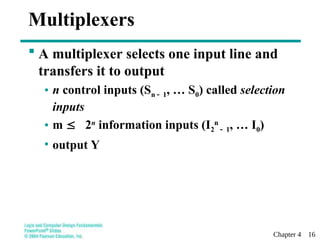
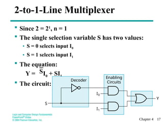
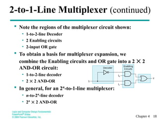
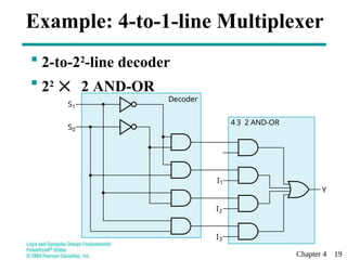
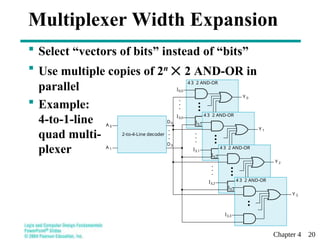
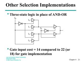
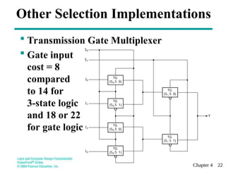
Charles Kime & Thomas Kaminski
© 2004 Pearson Education, Inc.
Terms of Use
(Hyperlinks are active in View Show mode)
Logic and Computer Design Fundamentals
Lecture 14 – Combinational Functional
Blocks
Chapter 4 2
Overview
 Functions and functional blocks
 Enabling
 Decoding
 Encoding
 Selecting
Chapter 4 3
Functions and Functional Blocks
 Higher-level functions
• Common in real designs
• Simplify design process
• Add hierarchy and replication
 Implemented within a functional block.
• In the past, many functional blocks were
implemented as SSI, MSI, and LSI chips.
 Today, they are often simply parts within a
VLSI circuits.
Chapter 4 4
Enabling Function
 Enabling permits an input signal to pass
through to an output
 Disabling blocks an input signal from passing
through to an output, replacing it with a fixed
value
 The value on the output when it is disable can
be Hi-Z (as for three-state buffers and
transmission gates), 0 , or 1
 When disabled, 0 output
 When disabled, 1 output
 See Example 4-2 in text
X
F
EN
(a)
EN
X
F
(b)
Chapter 4 5
 Decoding - the
• Conversion of n-bit input to m-bit output
• Given n m  2n
 Circuits that perform decoding are called
decoders
• Called n-to-m line decoders, where m  2n
, and
• Generate 2n
(or fewer) minterms for the n input
variables
Decoding
Chapter 4 6
 1-to-2-Line Decoder
 2-to-4-Line Decoder
 Note that the 2-4-line
made up of 2 1-to-2-
line decoders and 4 AND gates.
Decoder Examples
A D0 D1
0 1 0
1 0 1
(a) (b)
D1 5 A
A
D0 5 A
A1
0
0
1
1
A0
0
1
0
1
D0
1
0
0
0
D1
0
1
0
0
D2
0
0
1
0
D3
0
0
0
1
(a)
D0 5 A 1 A 0
D1 5 A 1 A 0
D2 5 A 1 A 0
D3 5 A 1 A 0
(b)
A 1
A 0
Chapter 4 7
Decoder Expansion - Example
 Result
3-to-8 Line decoder
1-to-2-Line decoders
4 2-input ANDs 8 2-input ANDs
2-to-4-Line
decoder
D0
A 0
A 1
A 2
D1
D2
D3
D4
D5
D6
D7
Chapter 4 8
 In general, attach m-enabling circuits to the outputs
 See truth table below for function
• Note use of X’s to denote both 0 and 1
• Combination containing two X’s represent four binary combinations
 Alternatively, can be viewed as distributing value of signal
EN to 1 of 4 outputs
 In this case, called a
demultiplexer
EN
A 1
A 0
D0
D1
D2
D3
(b)
EN A1 A0 D0 D1 D2 D3
0
1
1
1
1
X
0
0
1
1
X
0
1
0
1
0
1
0
0
0
0
0
1
0
0
0
0
0
1
0
0
0
0
0
Decoder with Enable
Chapter 4 9
Encoding
 Encoding - the opposite of decoding
• Conversion of m-bit input to n-bit output
 Circuits that perform encoding are called encoders
• An encoder has 2n
(or fewer) input lines and n output lines
which generate the binary code corresponding to the input
values
• Typically, an encoder converts a code containing exactly
one bit that is 1 to a binary code corres-ponding to the
position in which the 1 appears.
Chapter 4 10
Encoder Example
 A decimal-to-BCD encoder
• Inputs: 10 bits corresponding to decimal
digits 0 through 9, (D0, …, D9)
• Outputs: 4 bits with BCD codes
• Function: If input bit Di is a 1, then the
output (A3, A2, A1, A0) is the BCD code for i,
 The truth table could be formed, but
alternatively, the equations for each of the
four outputs can be obtained directly.
Chapter 4 11
Encoder Example (continued)
 Input Di is a term in equation Aj if bit Aj is 1
in the binary value for i.
 Equations:
A3 = D8 + D9
A2 = D4 + D5 + D6 + D7
A1 = D2 + D3 + D6 + D7
A0 = D1 + D3 + D5 + D7 + D9
0000
0001
0010
0011
0100
0101
0110
0111
1000
1001
Chapter 4 12
Priority Encoder
 What if multiple inputs are true?
• Encoder just designed does not work.
 Instead, use a priority encoder.
 Encodes either
• Most significant input position
• Or least significant input position
Chapter 4 13
Priority Encoder Example
 Priority encoder with 5 inputs (D4, D3, D2, D1, D0) - highest priority to most
significant 1 present - Code outputs A2, A1, A0 and V where V indicates at
least one 1 present.
 Xs in input part of table represent 0 or 1; thus table entries correspond to
product terms instead of minterms. The column on the left shows that all 32
minterms are present in the product terms in the table
No. of Min-
terms/Row
Inputs Outputs
D4 D3 D2 D1 D0 A2 A1 A0 V
1 0 0 0 0 0 X X X 0
1 0 0 0 0 1 0 0 0 1
2 0 0 0 1 X 0 0 1 1
4 0 0 1 X X 0 1 0 1
8 0 1 X X X 0 1 1 1
16 1 X X X X 1 0 0 1
Chapter 4 14
Priority Encoder Example (continued)
 Could use a K-map to get equations, but
can be read directly from table and
manually optimized if careful:
A2 = D4
A1 = D3 + D2 = F1, F1 = (D3 + D2)
A0 = D3 + D1 = (D3 + D1)
V = D4 + F1 + D1 + D0
D4 D3
D4 D4
D4 D3
D4 D2 D4 D2
Chapter 4 15
 Selecting of data or information is a critical
function in digital systems and computers
 Circuits that perform selecting have:
• A set of information inputs from which the selection
is made
• A single output
• A set of control lines for making the selection
 Logic circuits that perform selecting are called
multiplexers
 Selecting can also be done by three-state logic or
transmission gates
Selecting
Chapter 4 16
Multiplexers
 A multiplexer selects one input line and
transfers it to output
• n control inputs (Sn 1, … S0) called selection
inputs
• m  2n
information inputs (I2
n
1, … I0)
• output Y
Chapter 4 17
2-to-1-Line Multiplexer
 Since 2 = 21
, n = 1
 The single selection variable S has two values:
• S = 0 selects input I0
• S = 1 selects input I1
 The equation:
Y = I0 + SI1
 The circuit:
S
S
I0
I1
Decoder
Enabling
Circuits
Y
Chapter 4 18
2-to-1-Line Multiplexer (continued)
 Note the regions of the multiplexer circuit shown:
• 1-to-2-line Decoder
• 2 Enabling circuits
• 2-input OR gate
 To obtain a basis for multiplexer expansion, we
combine the Enabling circuits and OR gate into a 2  2
AND-OR circuit:
• 1-to-2-line decoder
• 2  2 AND-OR
 In general, for an 2n
-to-1-line multiplexer:
• n-to-2n
-line decoder
• 2n
 2 AND-OR
S
I0
I1
Decoder
Enabling
Circuits
Y
Chapter 4 19
Example: 4-to-1-line Multiplexer
 2-to-22
-line decoder
 22
 2 AND-OR
S1
Decoder
S0
Y
S1
Decoder
S0
Y
S1
Decoder
4 3 2 AND-OR
S0
Y
I2
I3
I1
Chapter 4 20
Multiplexer Width Expansion
 Select “vectors of bits” instead of “bits”
 Use multiple copies of 2n
 2 AND-OR in
parallel
 Example:
4-to-1-line
quad multi-
plexer
4 3 2 AND-OR
2-to-4-Line decoder
4 3 2 AND-OR
4 3 2 AND-OR
4 3 2 AND-OR
I0,0
I3,0
I0,1
I3,1
I0,2
I3,2
I0,3
I3,3
Y 0
D0
D3
A 0
A 1
Y 1
Y 2
Y 3
.
.
.
.
.
.
.
.
.
.
.
.
Chapter 4 21
Other Selection Implementations
 Three-state logic in place of AND-OR
 Gate input cost = 14 compared to 22 (or
18) for gate implementation
I0
I1
I2
I3
S1
S0
Chapter 4 22
Other Selection Implementations
 Transmission Gate Multiplexer
 Gate input
cost = 8
compared
to 14 for
3-state logic
and 18 or 22
for gate logic
S0
S1
I0
I1
I2
I3
Y
TG
(S0 5 0)
TG
(S1 5 0)
TG
(S1 5 1)
TG
(S0 5 1)
TG
(S0 5 0)
TG
(S0 5 1)
Chapter 4 23
Summary
 Functions and functional blocks
 Enabling
 Decoding
 Encoding
 Selecting with multiplexers
Chapter 4 24
Terms of Use
 © 2004 by Pearson Education,Inc. All rights reserved.
 The following terms of use apply in addition to the standard Pearson
Education Legal Notice.
 Permission is given to incorporate these materials into classroom
presentations and handouts only to instructors adopting Logic and
Computer Design Fundamentals as the course text.
 Permission is granted to the instructors adopting the book to post these
materials on a protected website or protected ftp site in original or
modified form. All other website or ftp postings, including those
offering the materials for a fee, are prohibited.
 You may not remove or in any way alter this Terms of Use notice or
any trademark, copyright, or other proprietary notice, including the
copyright watermark on each slide.
 Return to Title Page

leccccccccccc14_combinational_blocks.ppt

  • 1.
    Charles Kime &Thomas Kaminski © 2004 Pearson Education, Inc. Terms of Use (Hyperlinks are active in View Show mode) Logic and Computer Design Fundamentals Lecture 14 – Combinational Functional Blocks
  • 2.
    Chapter 4 2 Overview Functions and functional blocks  Enabling  Decoding  Encoding  Selecting
  • 3.
    Chapter 4 3 Functionsand Functional Blocks  Higher-level functions • Common in real designs • Simplify design process • Add hierarchy and replication  Implemented within a functional block. • In the past, many functional blocks were implemented as SSI, MSI, and LSI chips.  Today, they are often simply parts within a VLSI circuits.
  • 4.
    Chapter 4 4 EnablingFunction  Enabling permits an input signal to pass through to an output  Disabling blocks an input signal from passing through to an output, replacing it with a fixed value  The value on the output when it is disable can be Hi-Z (as for three-state buffers and transmission gates), 0 , or 1  When disabled, 0 output  When disabled, 1 output  See Example 4-2 in text X F EN (a) EN X F (b)
  • 5.
    Chapter 4 5 Decoding - the • Conversion of n-bit input to m-bit output • Given n m  2n  Circuits that perform decoding are called decoders • Called n-to-m line decoders, where m  2n , and • Generate 2n (or fewer) minterms for the n input variables Decoding
  • 6.
    Chapter 4 6 1-to-2-Line Decoder  2-to-4-Line Decoder  Note that the 2-4-line made up of 2 1-to-2- line decoders and 4 AND gates. Decoder Examples A D0 D1 0 1 0 1 0 1 (a) (b) D1 5 A A D0 5 A A1 0 0 1 1 A0 0 1 0 1 D0 1 0 0 0 D1 0 1 0 0 D2 0 0 1 0 D3 0 0 0 1 (a) D0 5 A 1 A 0 D1 5 A 1 A 0 D2 5 A 1 A 0 D3 5 A 1 A 0 (b) A 1 A 0
  • 7.
    Chapter 4 7 DecoderExpansion - Example  Result 3-to-8 Line decoder 1-to-2-Line decoders 4 2-input ANDs 8 2-input ANDs 2-to-4-Line decoder D0 A 0 A 1 A 2 D1 D2 D3 D4 D5 D6 D7
  • 8.
    Chapter 4 8 In general, attach m-enabling circuits to the outputs  See truth table below for function • Note use of X’s to denote both 0 and 1 • Combination containing two X’s represent four binary combinations  Alternatively, can be viewed as distributing value of signal EN to 1 of 4 outputs  In this case, called a demultiplexer EN A 1 A 0 D0 D1 D2 D3 (b) EN A1 A0 D0 D1 D2 D3 0 1 1 1 1 X 0 0 1 1 X 0 1 0 1 0 1 0 0 0 0 0 1 0 0 0 0 0 1 0 0 0 0 0 Decoder with Enable
  • 9.
    Chapter 4 9 Encoding Encoding - the opposite of decoding • Conversion of m-bit input to n-bit output  Circuits that perform encoding are called encoders • An encoder has 2n (or fewer) input lines and n output lines which generate the binary code corresponding to the input values • Typically, an encoder converts a code containing exactly one bit that is 1 to a binary code corres-ponding to the position in which the 1 appears.
  • 10.
    Chapter 4 10 EncoderExample  A decimal-to-BCD encoder • Inputs: 10 bits corresponding to decimal digits 0 through 9, (D0, …, D9) • Outputs: 4 bits with BCD codes • Function: If input bit Di is a 1, then the output (A3, A2, A1, A0) is the BCD code for i,  The truth table could be formed, but alternatively, the equations for each of the four outputs can be obtained directly.
  • 11.
    Chapter 4 11 EncoderExample (continued)  Input Di is a term in equation Aj if bit Aj is 1 in the binary value for i.  Equations: A3 = D8 + D9 A2 = D4 + D5 + D6 + D7 A1 = D2 + D3 + D6 + D7 A0 = D1 + D3 + D5 + D7 + D9 0000 0001 0010 0011 0100 0101 0110 0111 1000 1001
  • 12.
    Chapter 4 12 PriorityEncoder  What if multiple inputs are true? • Encoder just designed does not work.  Instead, use a priority encoder.  Encodes either • Most significant input position • Or least significant input position
  • 13.
    Chapter 4 13 PriorityEncoder Example  Priority encoder with 5 inputs (D4, D3, D2, D1, D0) - highest priority to most significant 1 present - Code outputs A2, A1, A0 and V where V indicates at least one 1 present.  Xs in input part of table represent 0 or 1; thus table entries correspond to product terms instead of minterms. The column on the left shows that all 32 minterms are present in the product terms in the table No. of Min- terms/Row Inputs Outputs D4 D3 D2 D1 D0 A2 A1 A0 V 1 0 0 0 0 0 X X X 0 1 0 0 0 0 1 0 0 0 1 2 0 0 0 1 X 0 0 1 1 4 0 0 1 X X 0 1 0 1 8 0 1 X X X 0 1 1 1 16 1 X X X X 1 0 0 1
  • 14.
    Chapter 4 14 PriorityEncoder Example (continued)  Could use a K-map to get equations, but can be read directly from table and manually optimized if careful: A2 = D4 A1 = D3 + D2 = F1, F1 = (D3 + D2) A0 = D3 + D1 = (D3 + D1) V = D4 + F1 + D1 + D0 D4 D3 D4 D4 D4 D3 D4 D2 D4 D2
  • 15.
    Chapter 4 15 Selecting of data or information is a critical function in digital systems and computers  Circuits that perform selecting have: • A set of information inputs from which the selection is made • A single output • A set of control lines for making the selection  Logic circuits that perform selecting are called multiplexers  Selecting can also be done by three-state logic or transmission gates Selecting
  • 16.
    Chapter 4 16 Multiplexers A multiplexer selects one input line and transfers it to output • n control inputs (Sn 1, … S0) called selection inputs • m  2n information inputs (I2 n 1, … I0) • output Y
  • 17.
    Chapter 4 17 2-to-1-LineMultiplexer  Since 2 = 21 , n = 1  The single selection variable S has two values: • S = 0 selects input I0 • S = 1 selects input I1  The equation: Y = I0 + SI1  The circuit: S S I0 I1 Decoder Enabling Circuits Y
  • 18.
    Chapter 4 18 2-to-1-LineMultiplexer (continued)  Note the regions of the multiplexer circuit shown: • 1-to-2-line Decoder • 2 Enabling circuits • 2-input OR gate  To obtain a basis for multiplexer expansion, we combine the Enabling circuits and OR gate into a 2  2 AND-OR circuit: • 1-to-2-line decoder • 2  2 AND-OR  In general, for an 2n -to-1-line multiplexer: • n-to-2n -line decoder • 2n  2 AND-OR S I0 I1 Decoder Enabling Circuits Y
  • 19.
    Chapter 4 19 Example:4-to-1-line Multiplexer  2-to-22 -line decoder  22  2 AND-OR S1 Decoder S0 Y S1 Decoder S0 Y S1 Decoder 4 3 2 AND-OR S0 Y I2 I3 I1
  • 20.
    Chapter 4 20 MultiplexerWidth Expansion  Select “vectors of bits” instead of “bits”  Use multiple copies of 2n  2 AND-OR in parallel  Example: 4-to-1-line quad multi- plexer 4 3 2 AND-OR 2-to-4-Line decoder 4 3 2 AND-OR 4 3 2 AND-OR 4 3 2 AND-OR I0,0 I3,0 I0,1 I3,1 I0,2 I3,2 I0,3 I3,3 Y 0 D0 D3 A 0 A 1 Y 1 Y 2 Y 3 . . . . . . . . . . . .
  • 21.
    Chapter 4 21 OtherSelection Implementations  Three-state logic in place of AND-OR  Gate input cost = 14 compared to 22 (or 18) for gate implementation I0 I1 I2 I3 S1 S0
  • 22.
    Chapter 4 22 OtherSelection Implementations  Transmission Gate Multiplexer  Gate input cost = 8 compared to 14 for 3-state logic and 18 or 22 for gate logic S0 S1 I0 I1 I2 I3 Y TG (S0 5 0) TG (S1 5 0) TG (S1 5 1) TG (S0 5 1) TG (S0 5 0) TG (S0 5 1)
  • 23.
    Chapter 4 23 Summary Functions and functional blocks  Enabling  Decoding  Encoding  Selecting with multiplexers
  • 24.
    Chapter 4 24 Termsof Use  © 2004 by Pearson Education,Inc. All rights reserved.  The following terms of use apply in addition to the standard Pearson Education Legal Notice.  Permission is given to incorporate these materials into classroom presentations and handouts only to instructors adopting Logic and Computer Design Fundamentals as the course text.  Permission is granted to the instructors adopting the book to post these materials on a protected website or protected ftp site in original or modified form. All other website or ftp postings, including those offering the materials for a fee, are prohibited.  You may not remove or in any way alter this Terms of Use notice or any trademark, copyright, or other proprietary notice, including the copyright watermark on each slide.  Return to Title Page

Editor's Notes

  • #11 No. The total gate input cost remains the same.
  • #13 Go over table explaining how entries were obtained, particularly those containing Xs