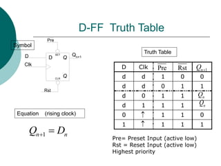
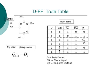
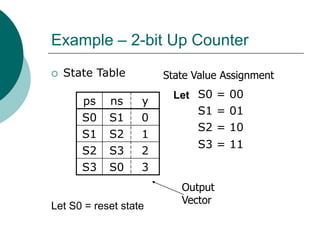
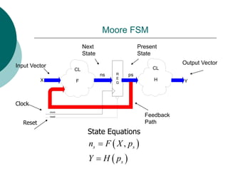
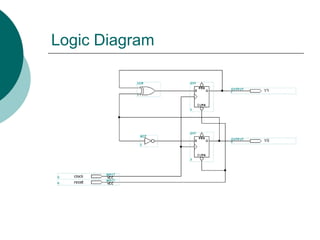
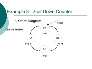
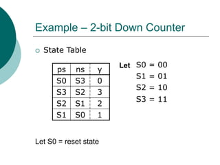
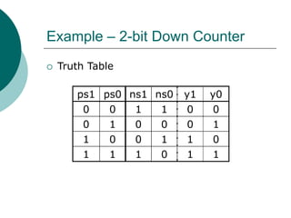
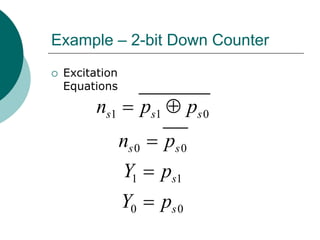
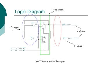
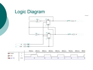
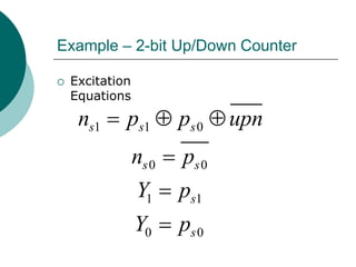
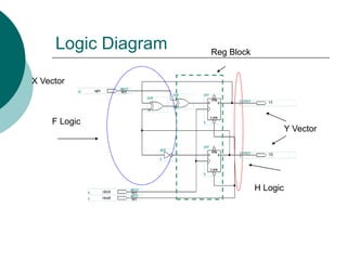
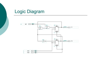
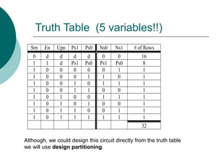
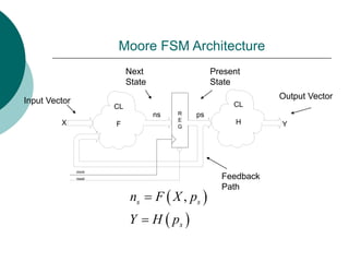
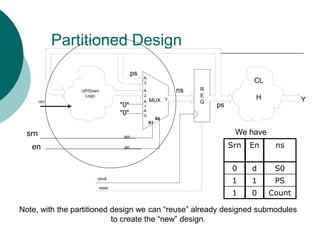
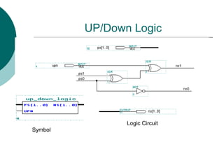
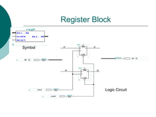
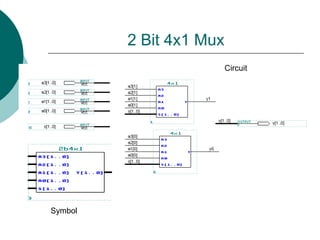
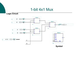
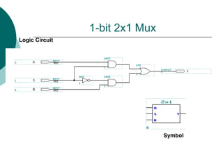
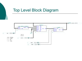
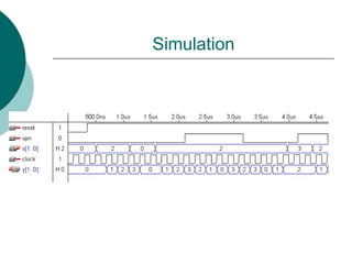
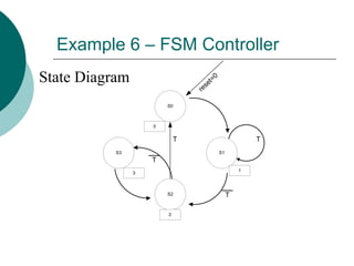
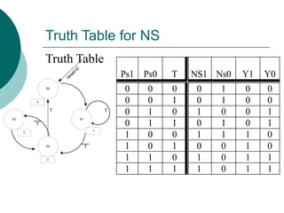
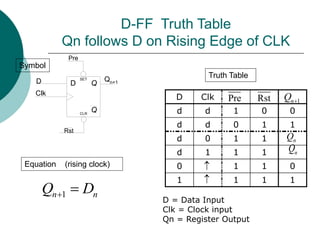
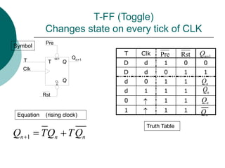
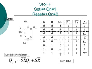
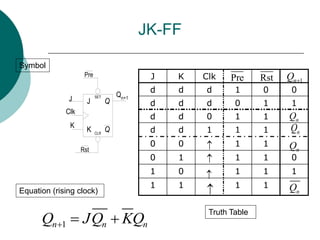
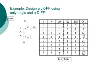
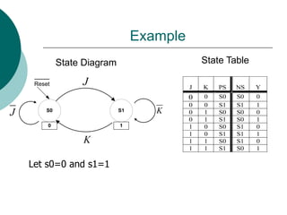
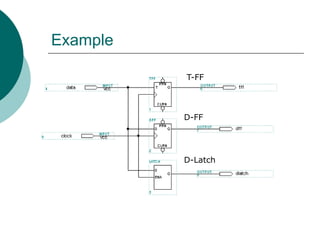
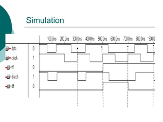
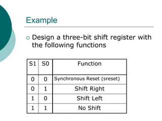
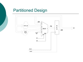
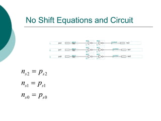
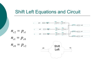
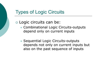
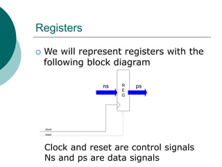
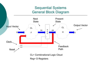
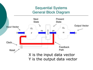
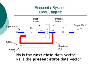
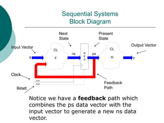
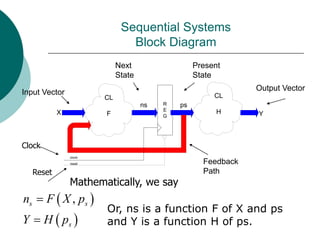
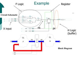
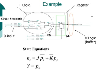
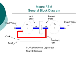
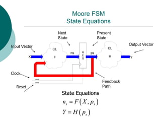
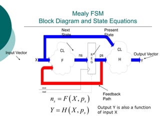
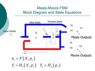
Sequential logic circuits have memory elements that allow the output to depend not just on the current inputs but also on previous inputs. Common memory elements are D flip-flops which have a data input, clock input, and output that changes on the rising or falling edge of the clock. Finite state machines (FSMs) can be modeled as Moore or Mealy machines using state tables and diagrams to design circuits like counters that change state based on inputs. Registers are added to combinational logic circuits to create sequential circuits.
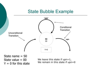
![State Bubble
Name
[Value]
Output
[Conditional]
State
(transition)](https://image.slidesharecdn.com/05chapter678-sequential-design-240114133958-7090f41d/85/05_Chapter-6-7-8-Sequential-design-ppt-23-320.jpg)