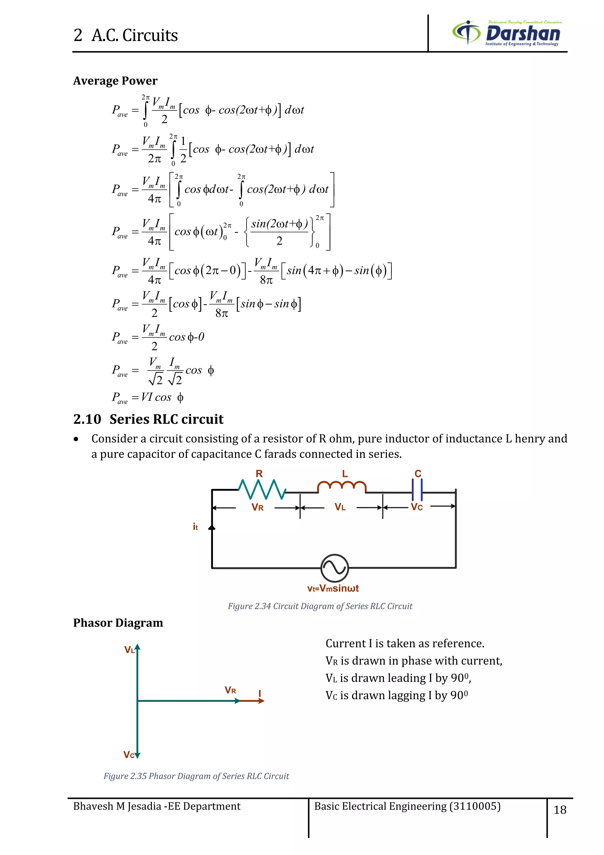
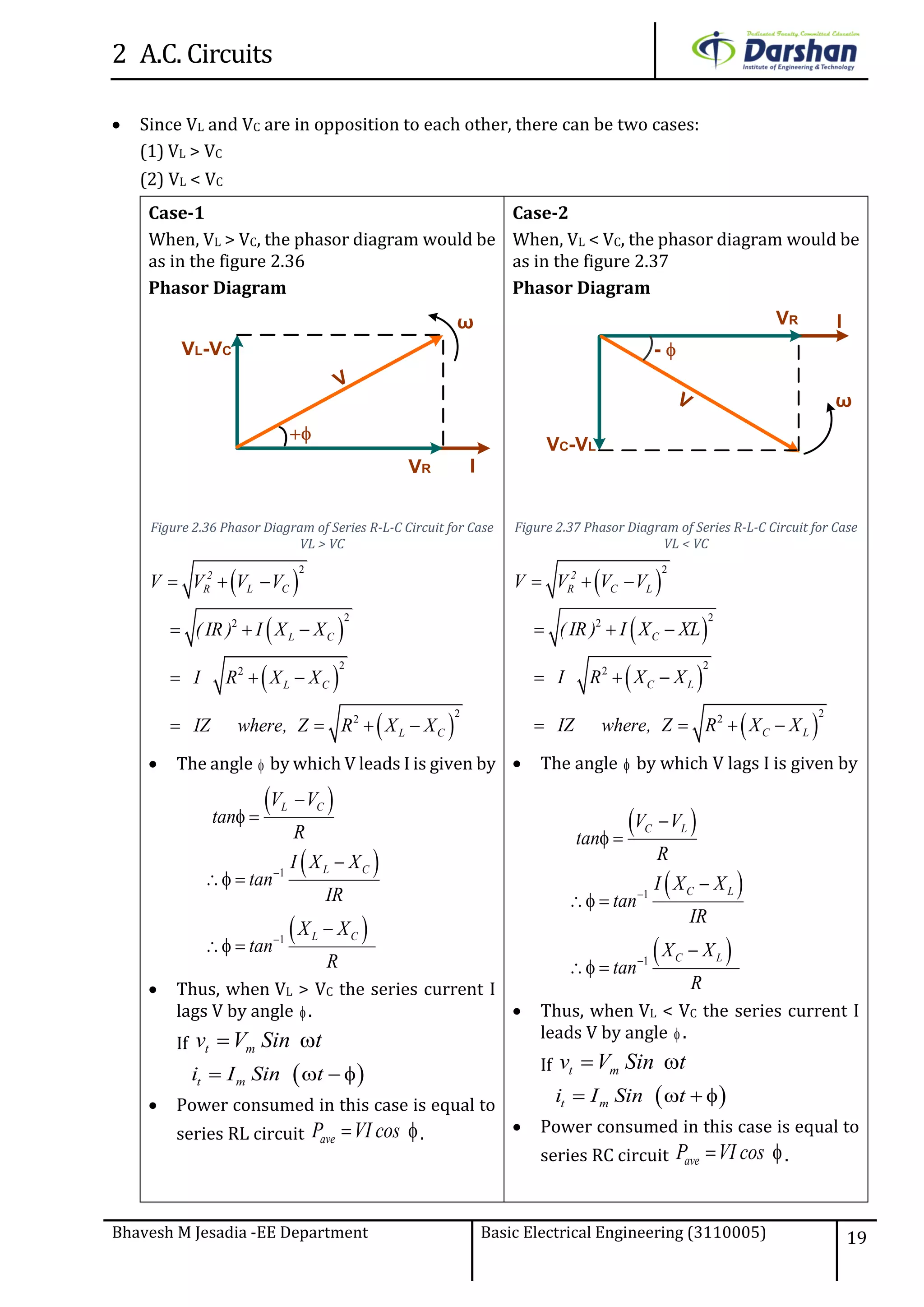
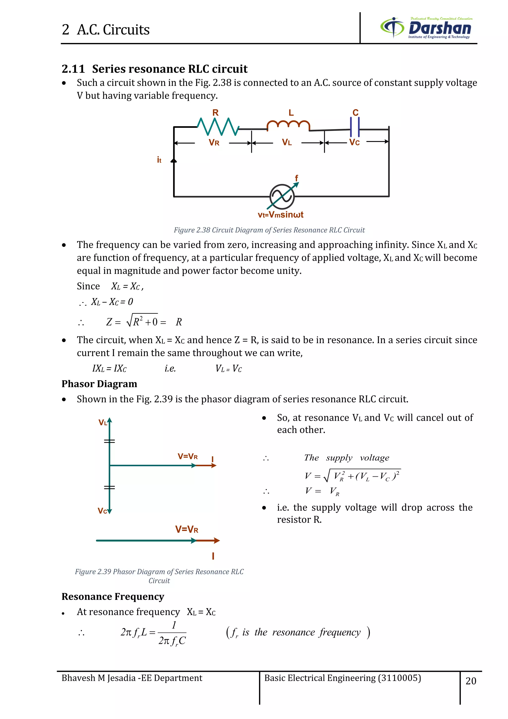
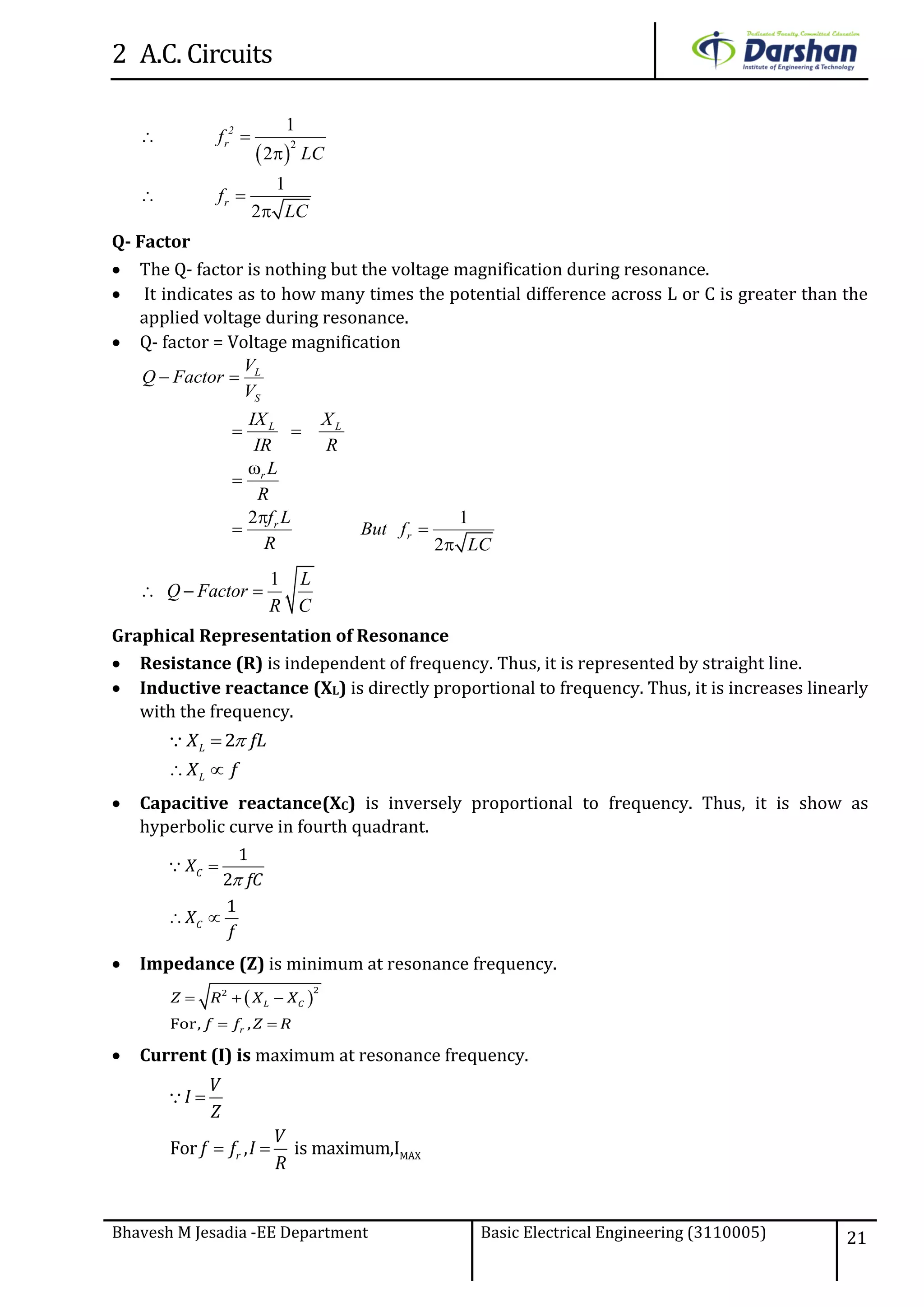
Downloaded 87 times
![2 A.C. Circuits
Bhavesh M Jesadia -EE Department Basic Electrical Engineering (3110005) 1
Single - Phase AC Circuits
2.1 Equation for generation of alternating induce EMF
An AC generator uses the principle of Faraday’s electromagnetic induction law. It states that
when current carrying conductor cut the magnetic field then emf induced in the conductor.
Inside this magnetic field a single rectangular loop of wire rotes around a fixed axis allowing
it to cut the magnetic flux at various angles as shown below figure 2.1.
N S
Axis of Rotation
Axis of Rotation
Magnetic Flux
Magnetic Pole
Wire
Loop(Conductor)
Wire
Loop(Conductor)
Figure 2.2.1 Generation of EMF
Where,
N =No. of turns of coil
A = Area of coil (m2)
ω=Angular velocity (radians/second)
m= Maximum flux (wb)
When coil is along XX’ (perpendicular to the lines of flux), flux linking with coil= m. When
coil is along YY’ (parallel to the lines of flux), flux linking with the coil is zero. When coil is
making an angle with respect to XX’ flux linking with coil, = m cosωt [ = ωt].
SN
ωt
X
X’
m cosωt
m sinωt
YY’
Figure 2.2 Alternating Induced EMF
According to Faraday’s law of electromagnetic induction,
Where,
2
m m
m m
2
m
2
E N
N no. of turns of the coil
B A
B Maximum flux density (wb/m )
A Area of the coil (m )
f
m
m
m
m
d
e N
dt
( cos t )
e Nd
dt
e N ( sin t )
e N sin t
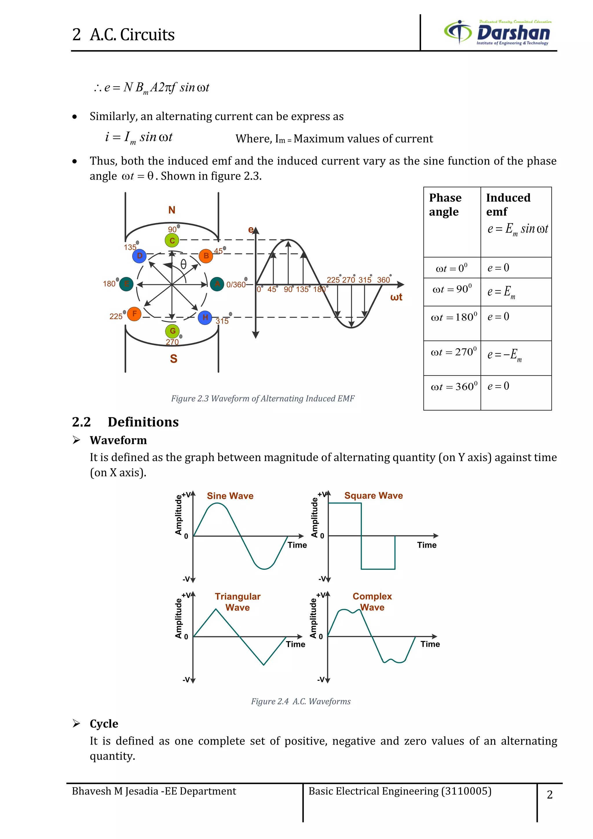
e E sin t](https://image.slidesharecdn.com/e-notespdfunit-218052019084740am-190722033844/75/Basic-Electrical-Engineering-AC-Circuit-1-2048.jpg)
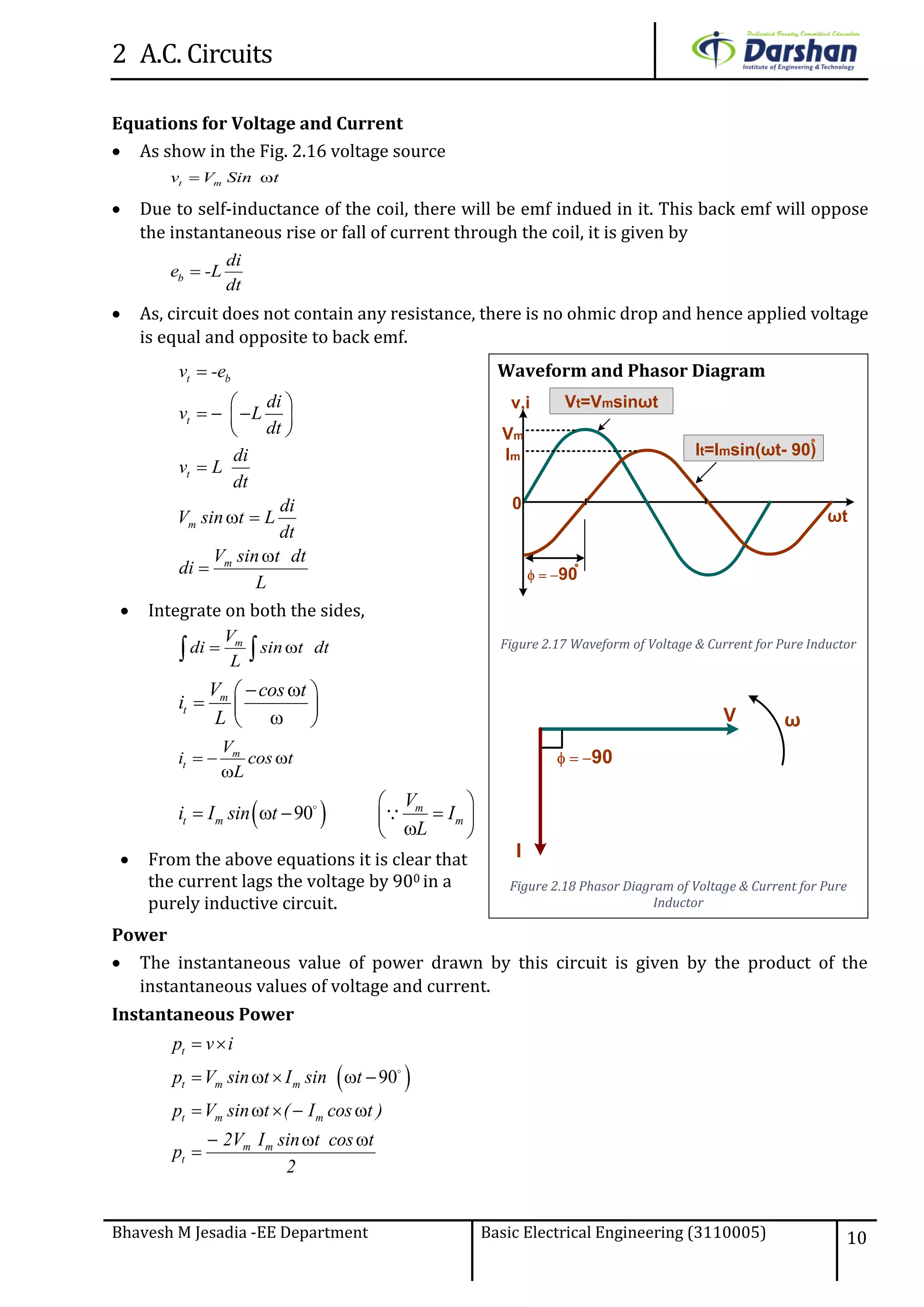
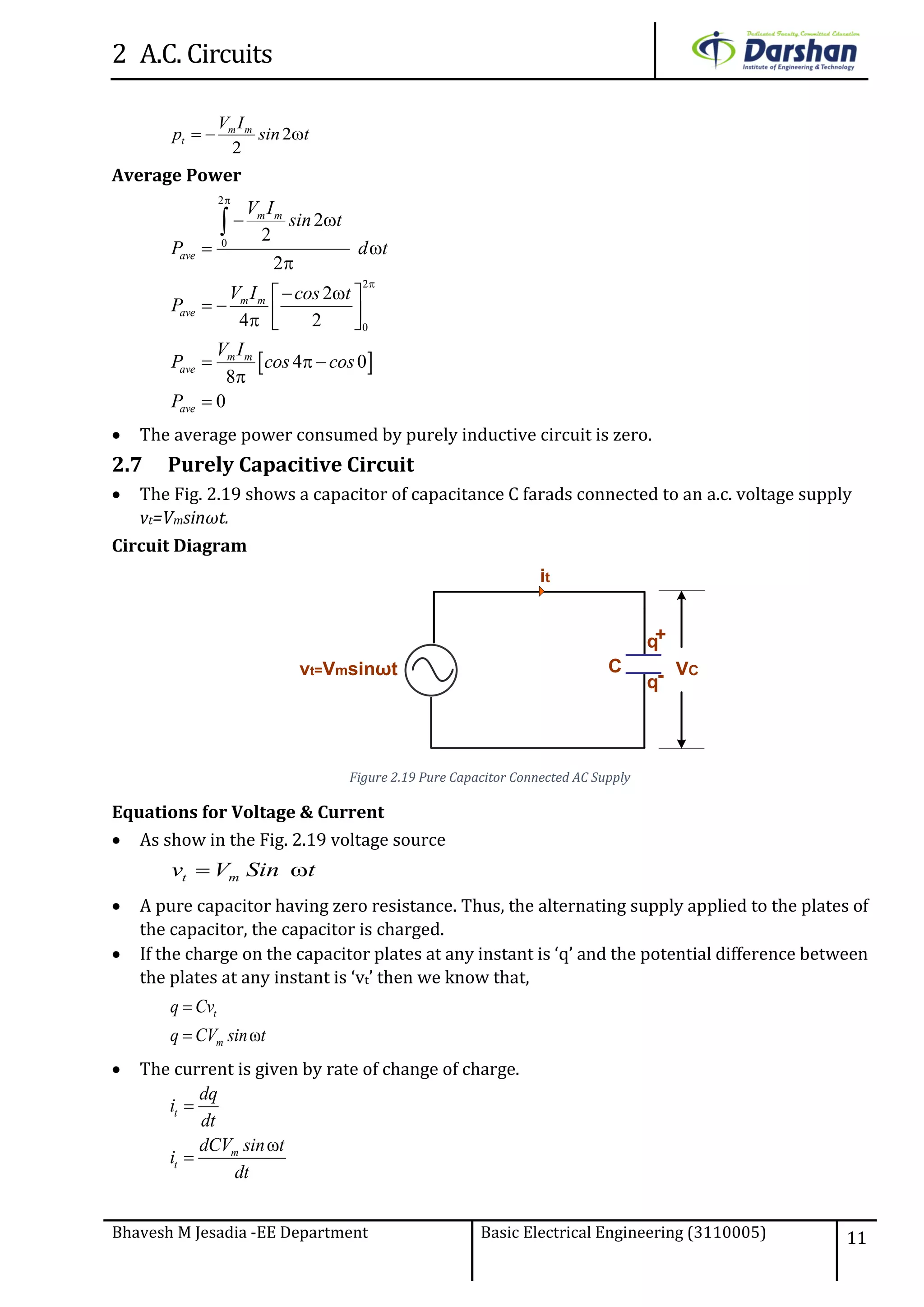
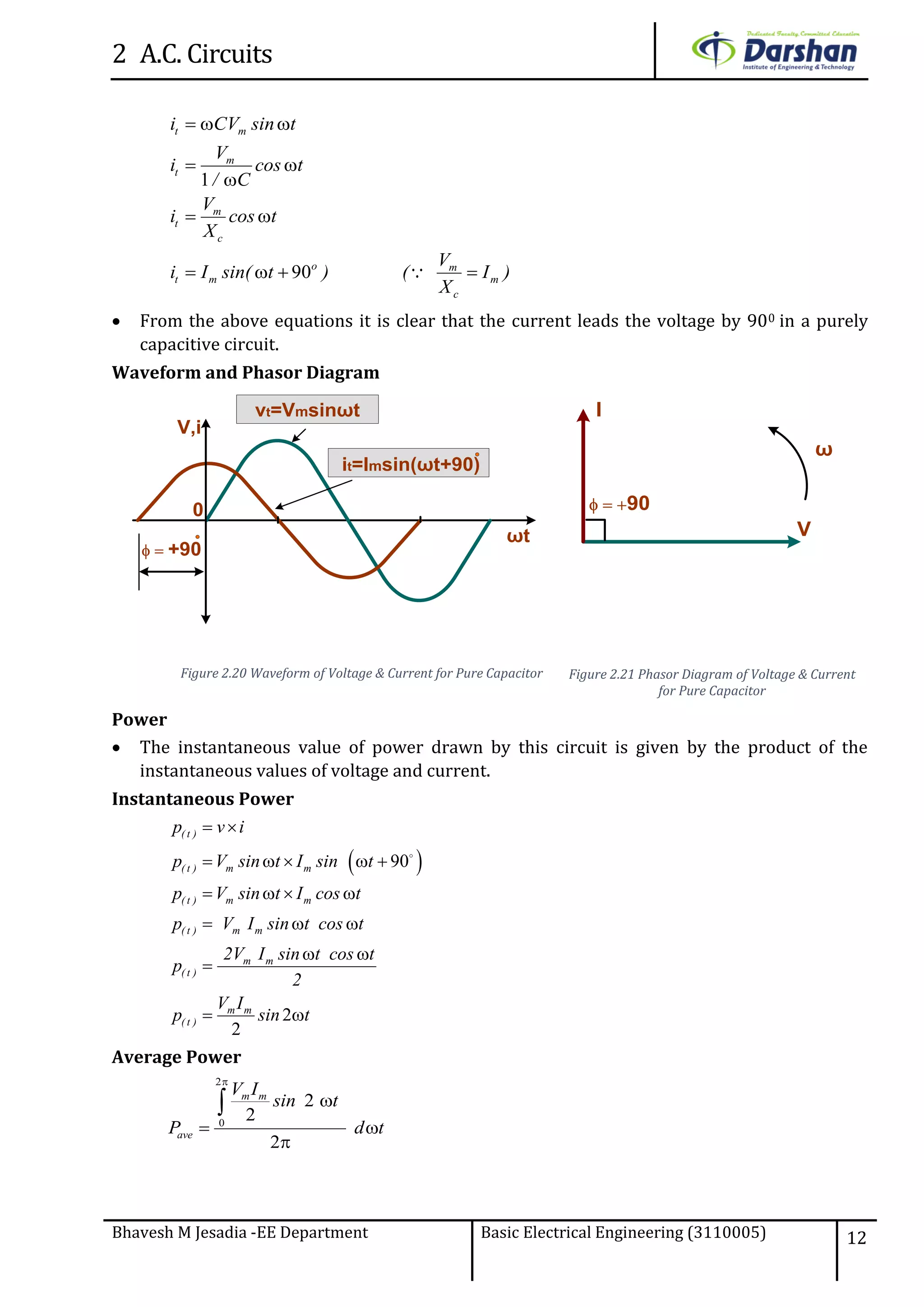
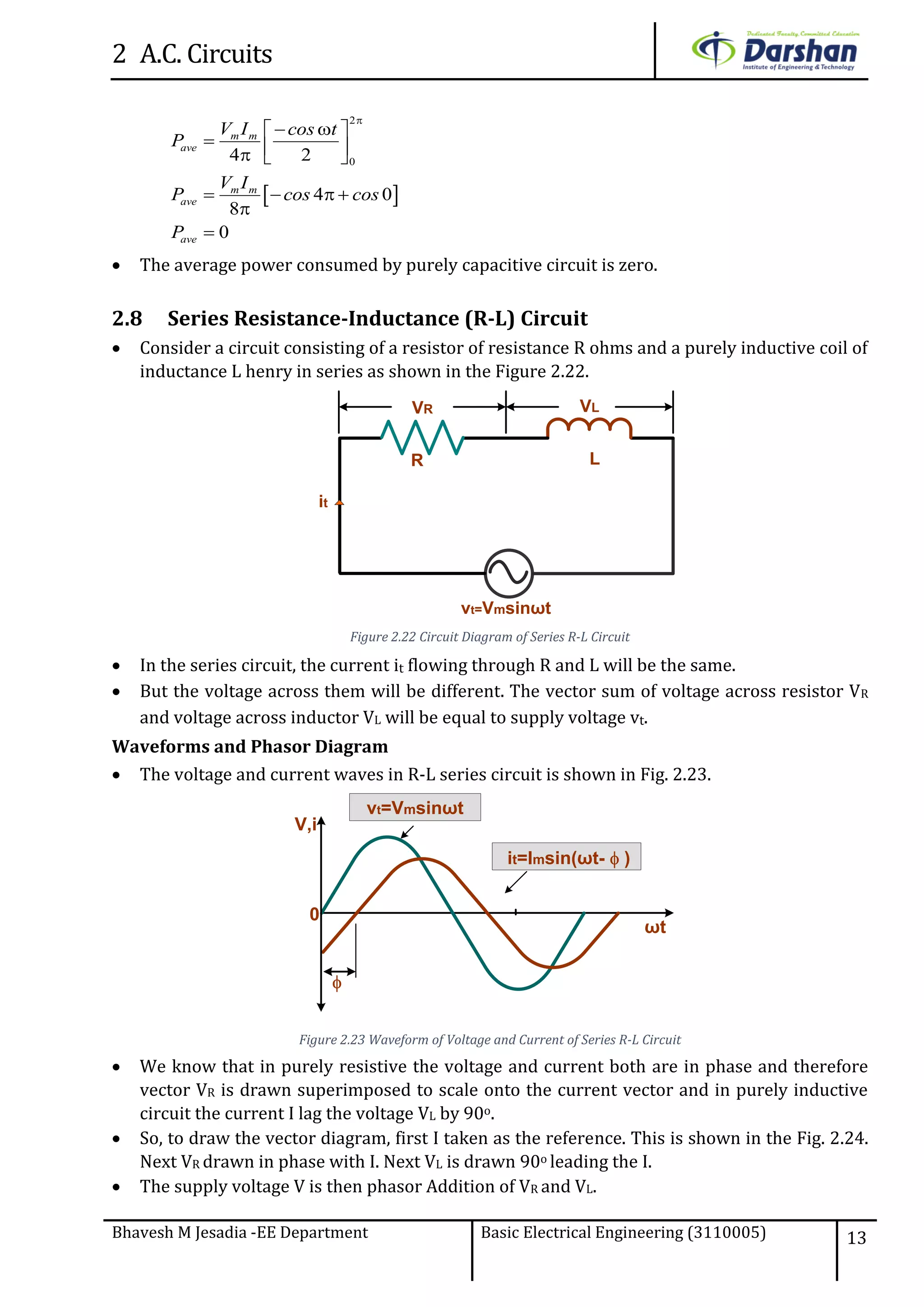

This document discusses alternating current (AC) circuits. It begins by describing how an alternating electromotive force (EMF) is generated using a coil rotating in a magnetic field. Equations are provided showing that both the induced EMF and current vary as sine functions. Common terms used in AC circuits like cycle, frequency, phase, and root mean square (RMS) value are defined. Phasor diagrams are introduced to represent AC quantities in terms of magnitude and direction. Derivations of average and RMS values are shown. Finally, a purely resistive AC circuit is analyzed, showing the current is in phase with voltage and both follow sine waves. Power calculations are also demonstrated.


![AC_CIRCUITS[1].pptx](https://cdn.slidesharecdn.com/ss_thumbnails/accircuits1-230813170350-dc7f310b-thumbnail.jpg?width=640&height=640&fit=bounds)

![BEE-Unit 2-AC Circuits[1].pdf7ft7fg7f7g7g7g7g7g77g7g8gg8ggg8g8g8g8h8hh88hh8hh...](https://cdn.slidesharecdn.com/ss_thumbnails/bee-unit2-accircuits1-250330063149-c808a509-thumbnail.jpg?width=640&height=640&fit=bounds)


