Downloaded 162 times
![19
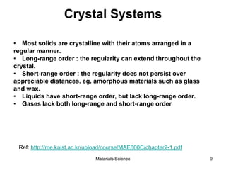
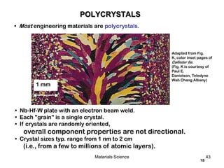
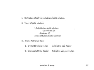
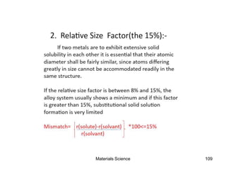
• Single Crystals
-Properties vary with
direction: anisotropic.
-Example: the modulus
of elasticity (E) in BCC iron:
• Polycrystals
-Properties may/may not
vary with direction.
-If grains are randomly
oriented: isotropic.
(Epoly iron = 210 GPa)
-If grains are textured,
anisotropic.
200 m
Data from Table
3.3, Callister 6e.
(Source of data is
R.W.
Hertzberg, Deformatio
n and Fracture
Mechanics of
Engineering
Materials, 3rd
ed., John Wiley and
Sons, 1989.)
Adapted from Fig.
4.12(b), Callister 6e.
(Fig. 4.12(b) is
courtesy of L.C. Smith
and C. Brady, the
National Bureau of
Standards,
Washington, DC [now
the National Institute
of Standards and
Technology,
Gaithersburg, MD].)
SINGLE VS POLYCRYSTALS
44Materials Science](https://image.slidesharecdn.com/crystalography-140401234432-phpapp01/85/Crystalography-44-320.jpg)
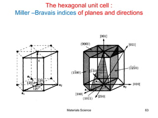
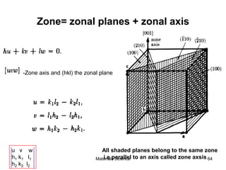
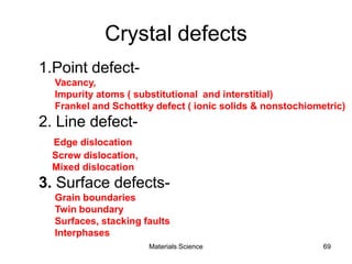
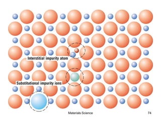
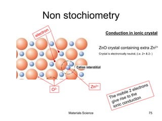
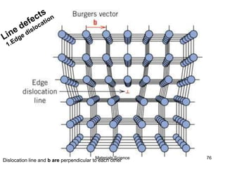
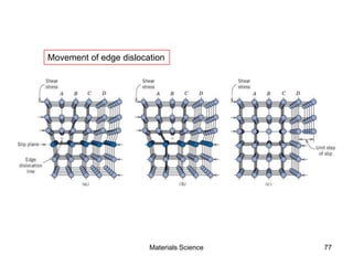

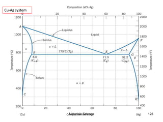
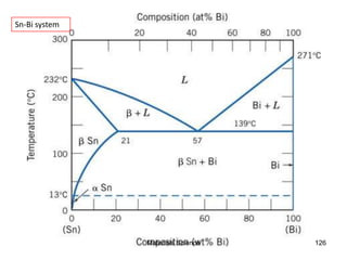
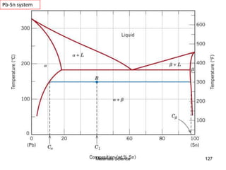
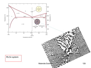

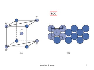
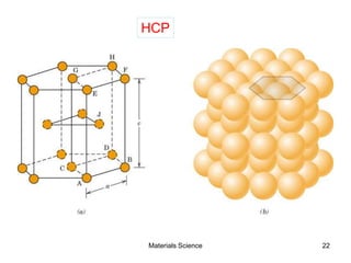
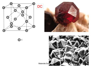
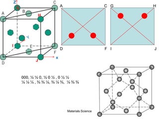
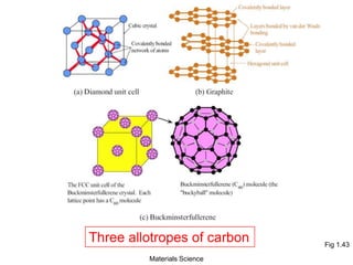
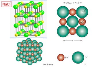
This document provides an overview of materials science concepts including: - Crystal structures such as FCC, BCC, and HCP. Defects like point defects, line defects, and dislocations are also introduced. - Principles of alloy formation including solid solutions and binary phase diagrams. Common systems like Cu-Ni and Fe-C are discussed. - Crystallography topics such as Miller indices, lattice planes, zone axes, and crystal directions. - Differences between single crystals and polycrystals and how they impact material properties. - Additional concepts covered include defects in ionic crystals, non-stoichiometry, and dislocation movement.


