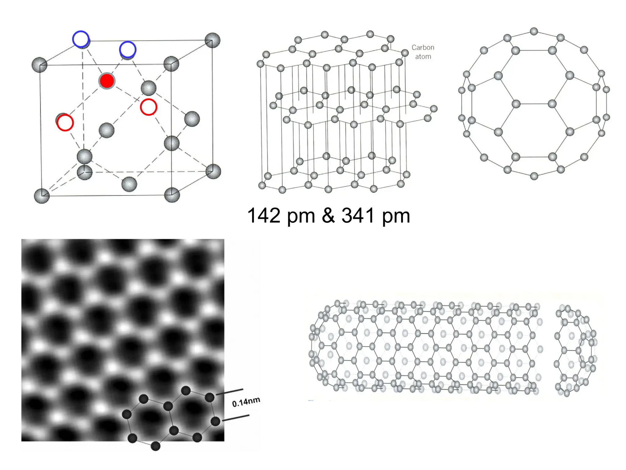
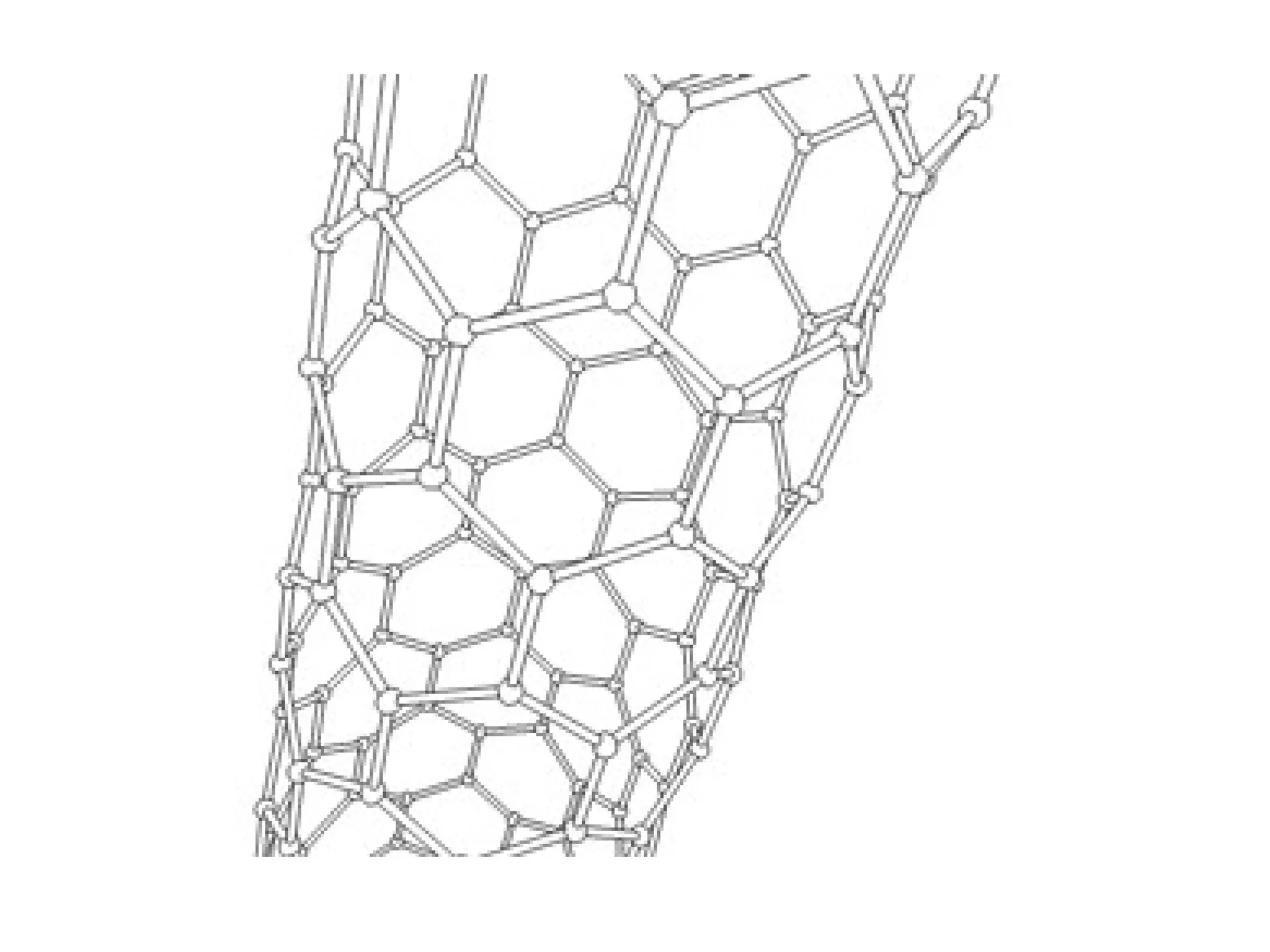
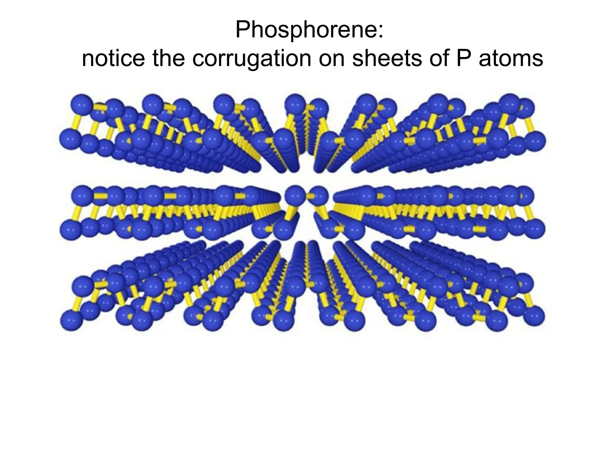
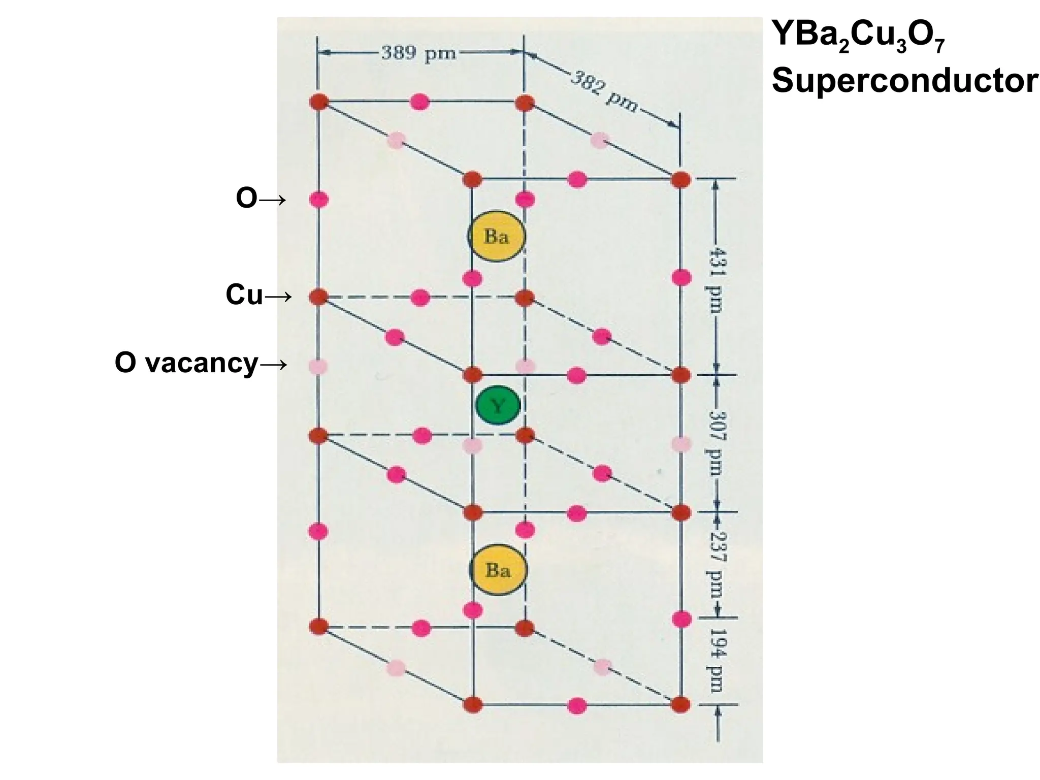
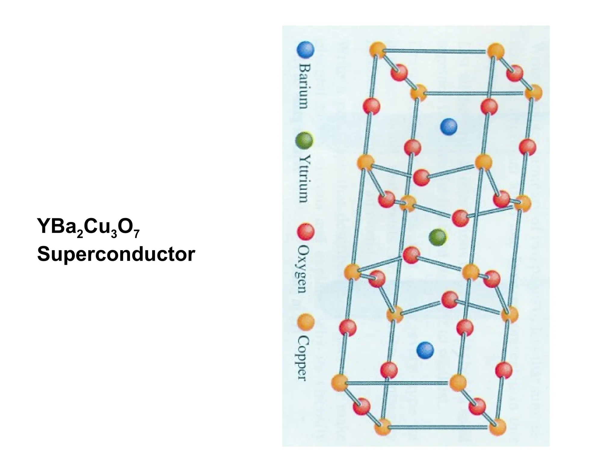
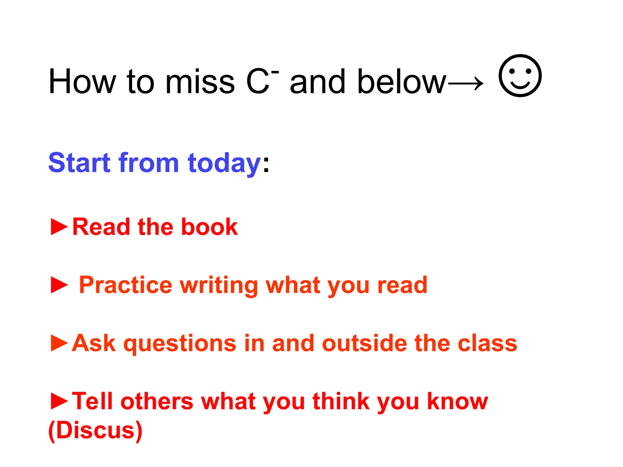
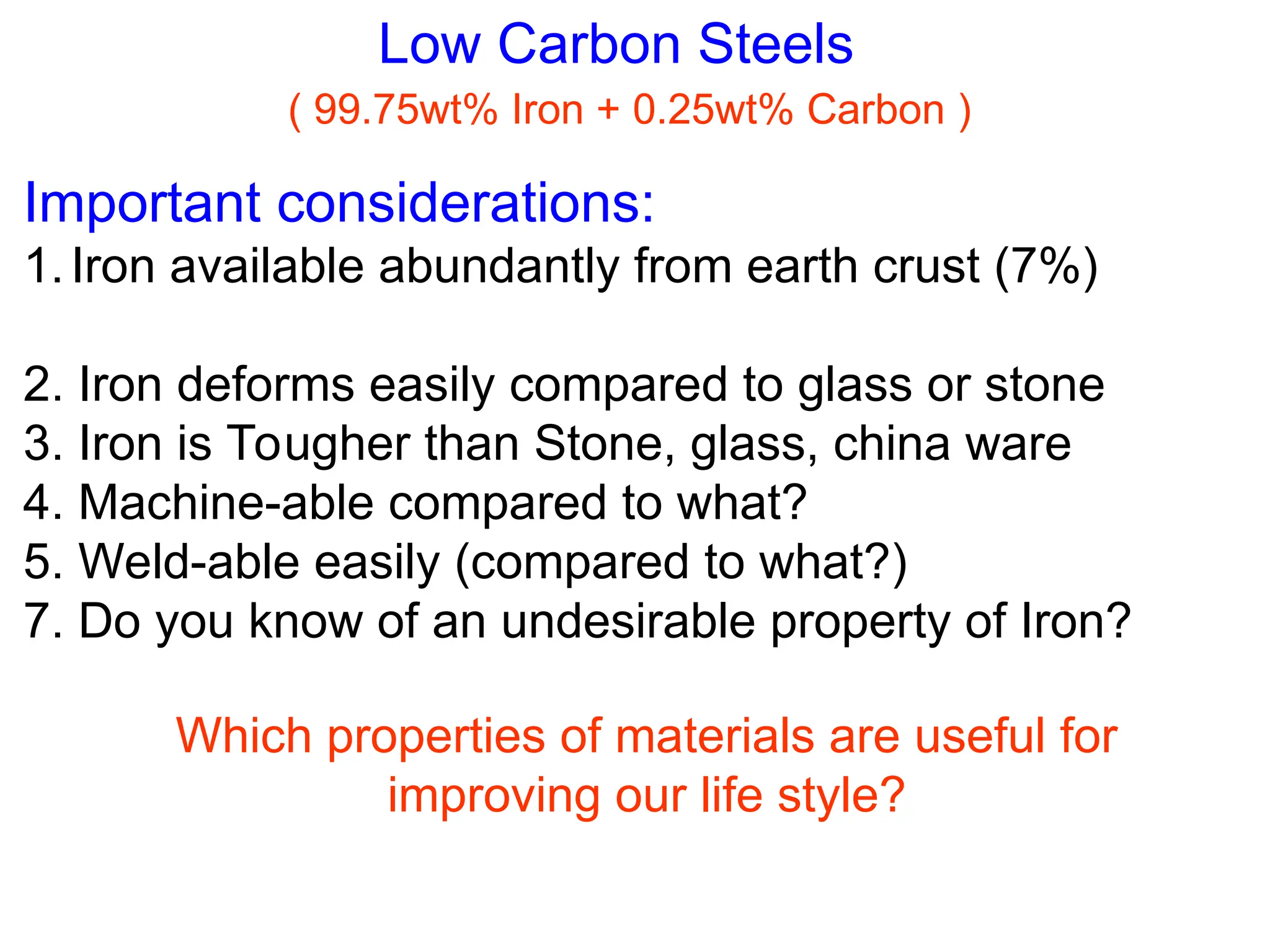
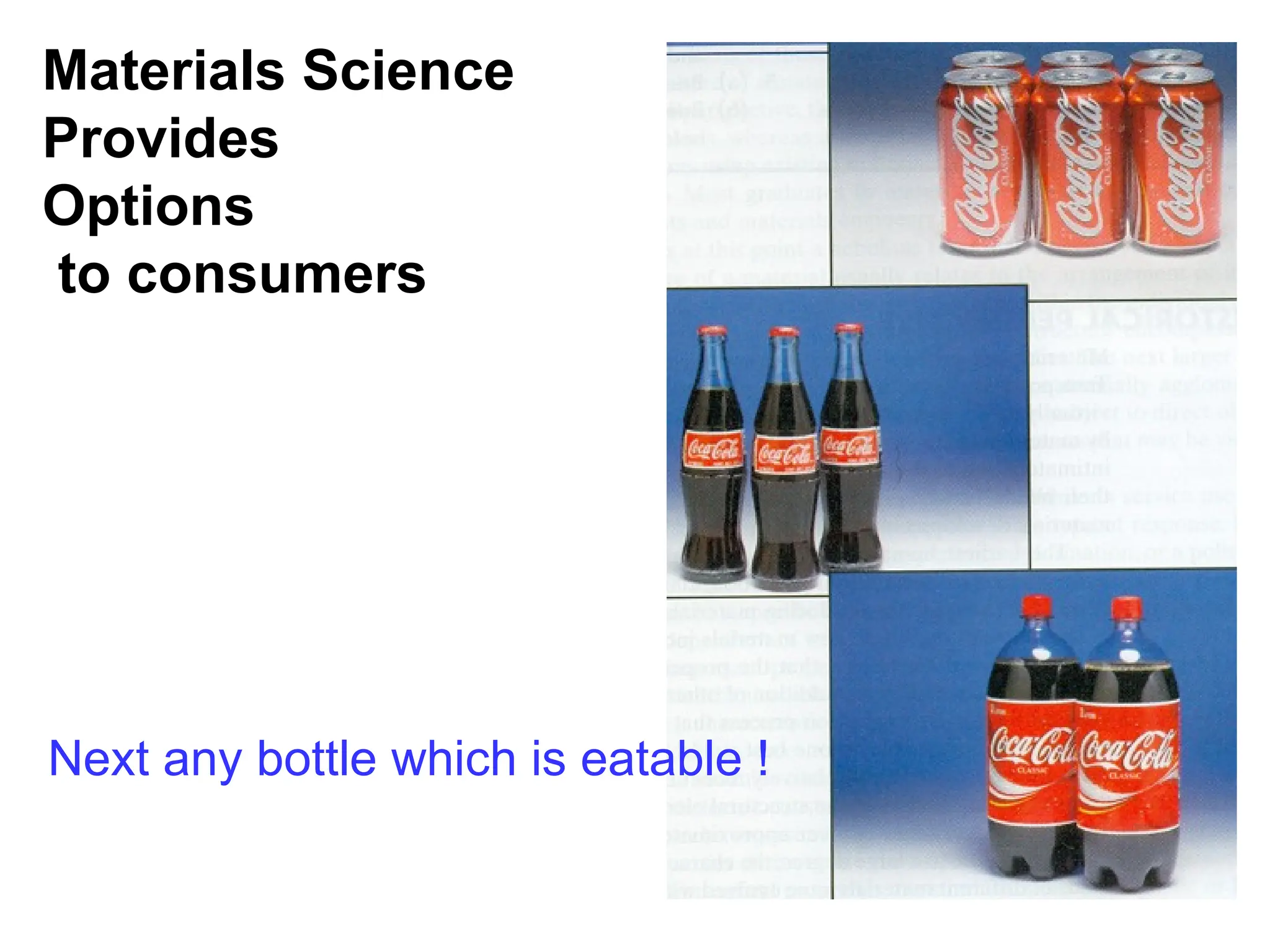
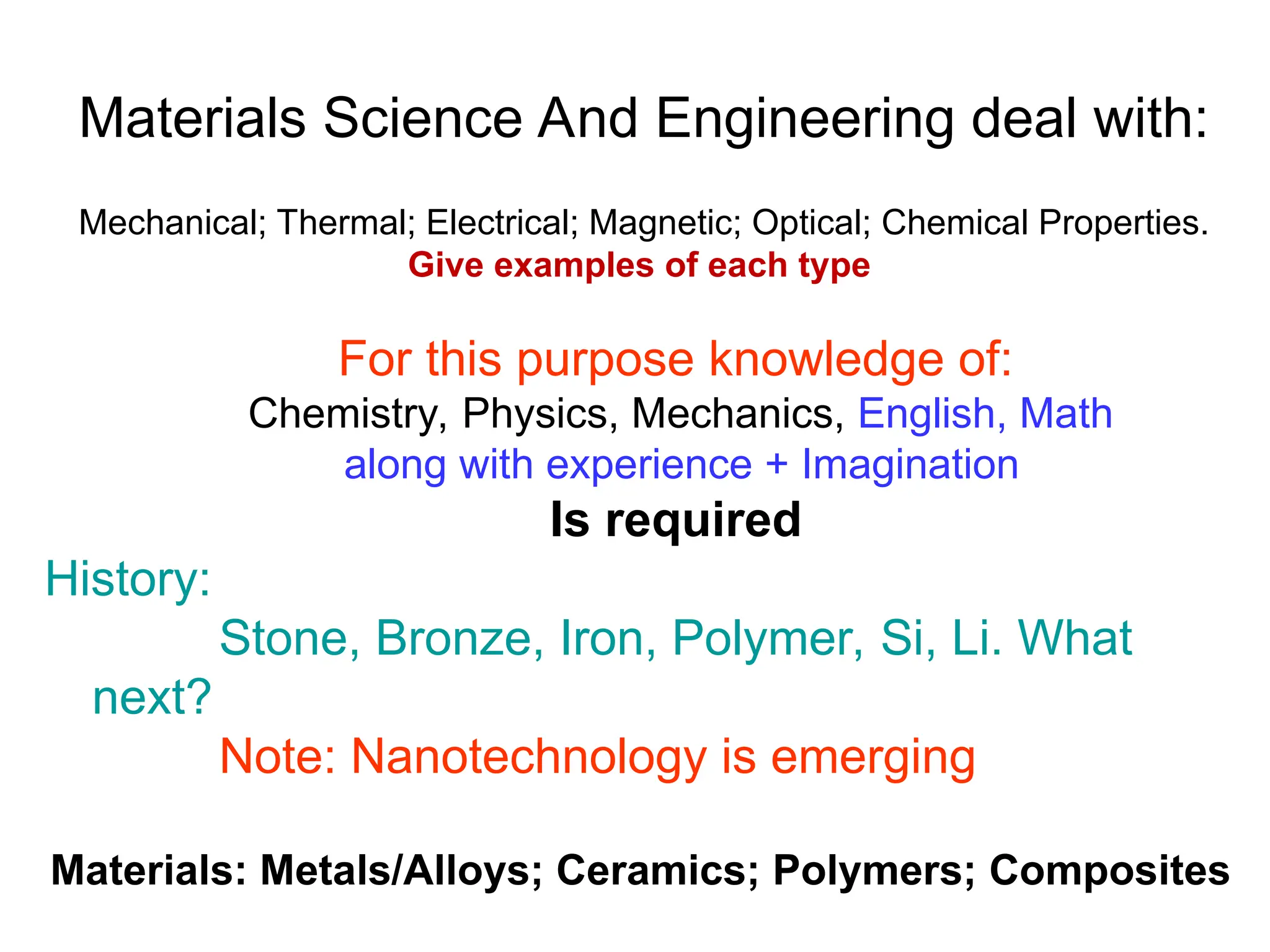
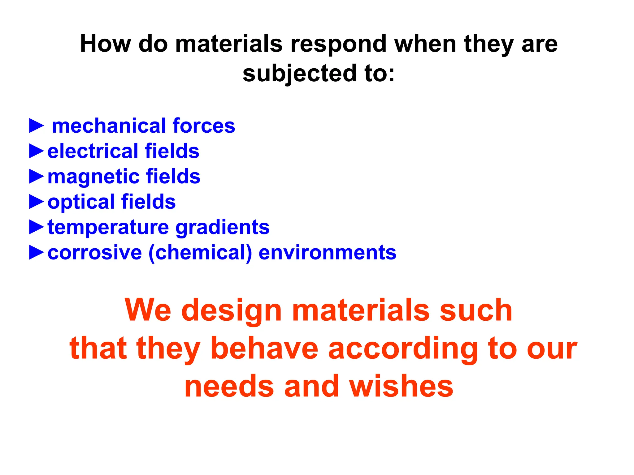
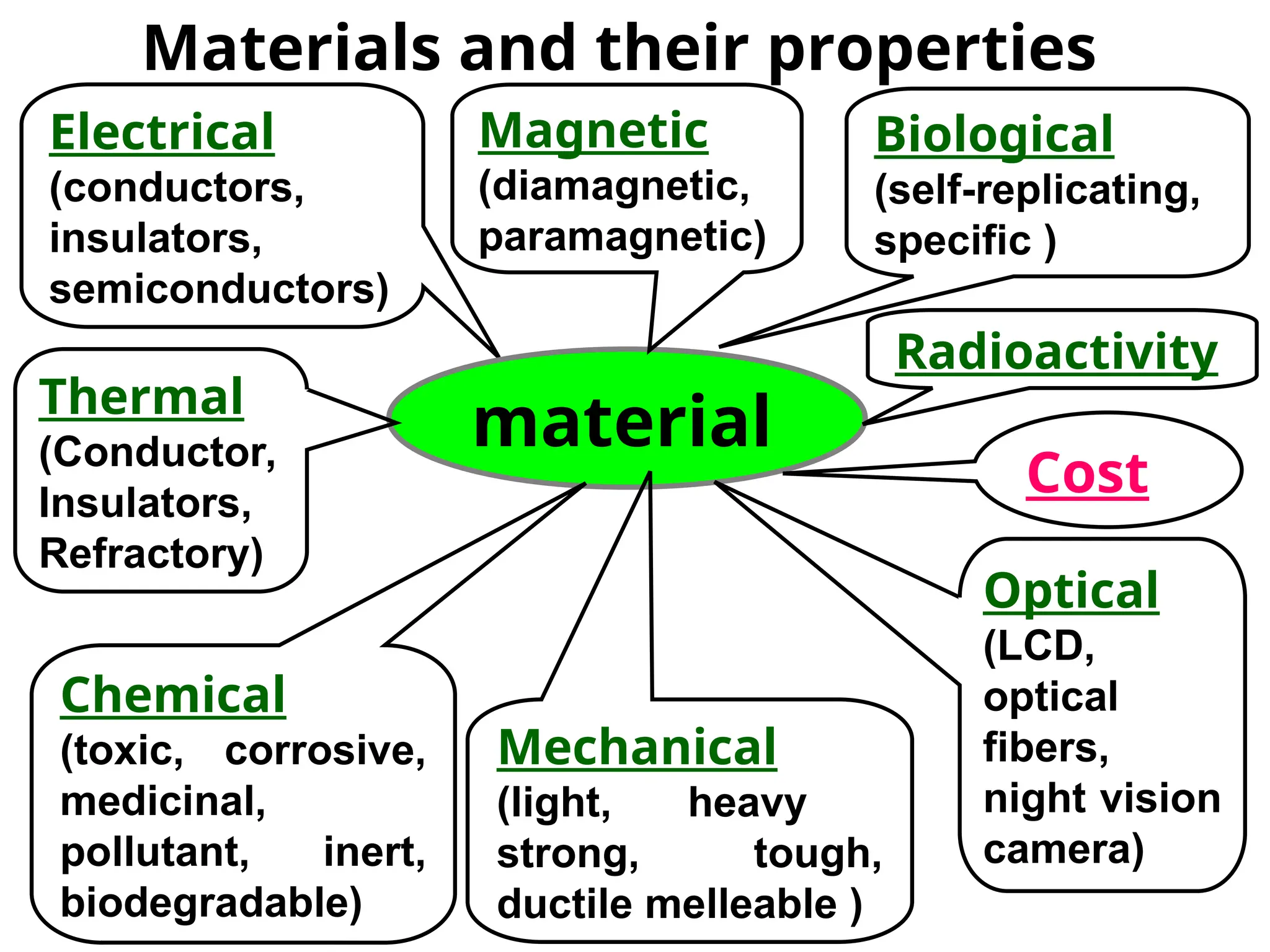
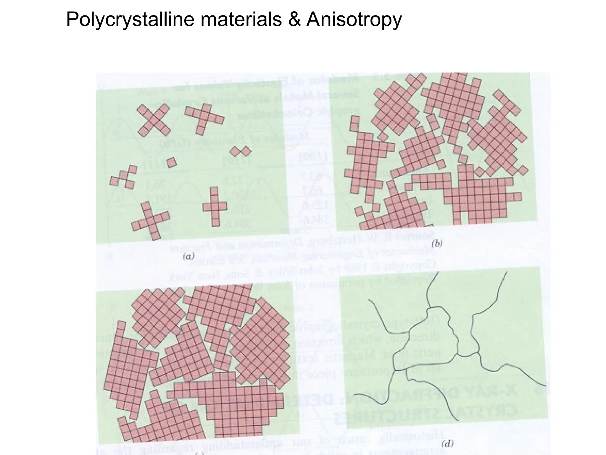
Engineering materials are substances and compounds used to build structures, machines, and devices, selected for their ability to withstand loads and perform specific functions. They are classified into major categories such as metals, polymers, ceramics, and composites, each with unique mechanical, thermal, and electrical properties.
![MM102: Introduction to Engineering Materials. Spring Semester 2019
Course Instructors: Dr. Shanza Rehan, Eng. Ali Afraz & Dr. Fida Mohammad
1. Text Book: Materials Science and Engineering: An Introduction
Callister and Rethwisch. 9th
Edition, 2014
2.Reference: Foundation of Materials Science and Engineering,
Smith & Hashemi. 4th
Edition 2006
Chapter 1 for self study
Chapter 2: Two Lect.: Grading policy & Introduction
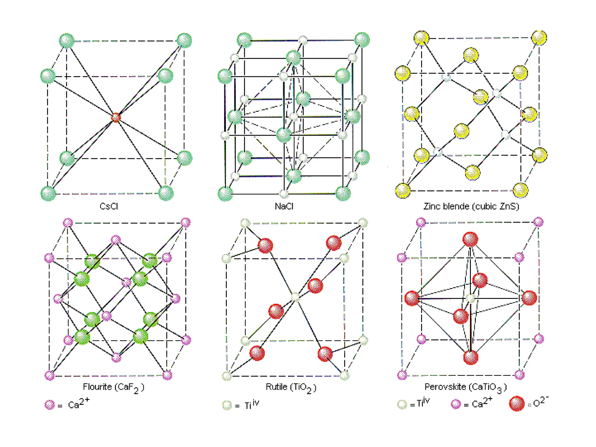
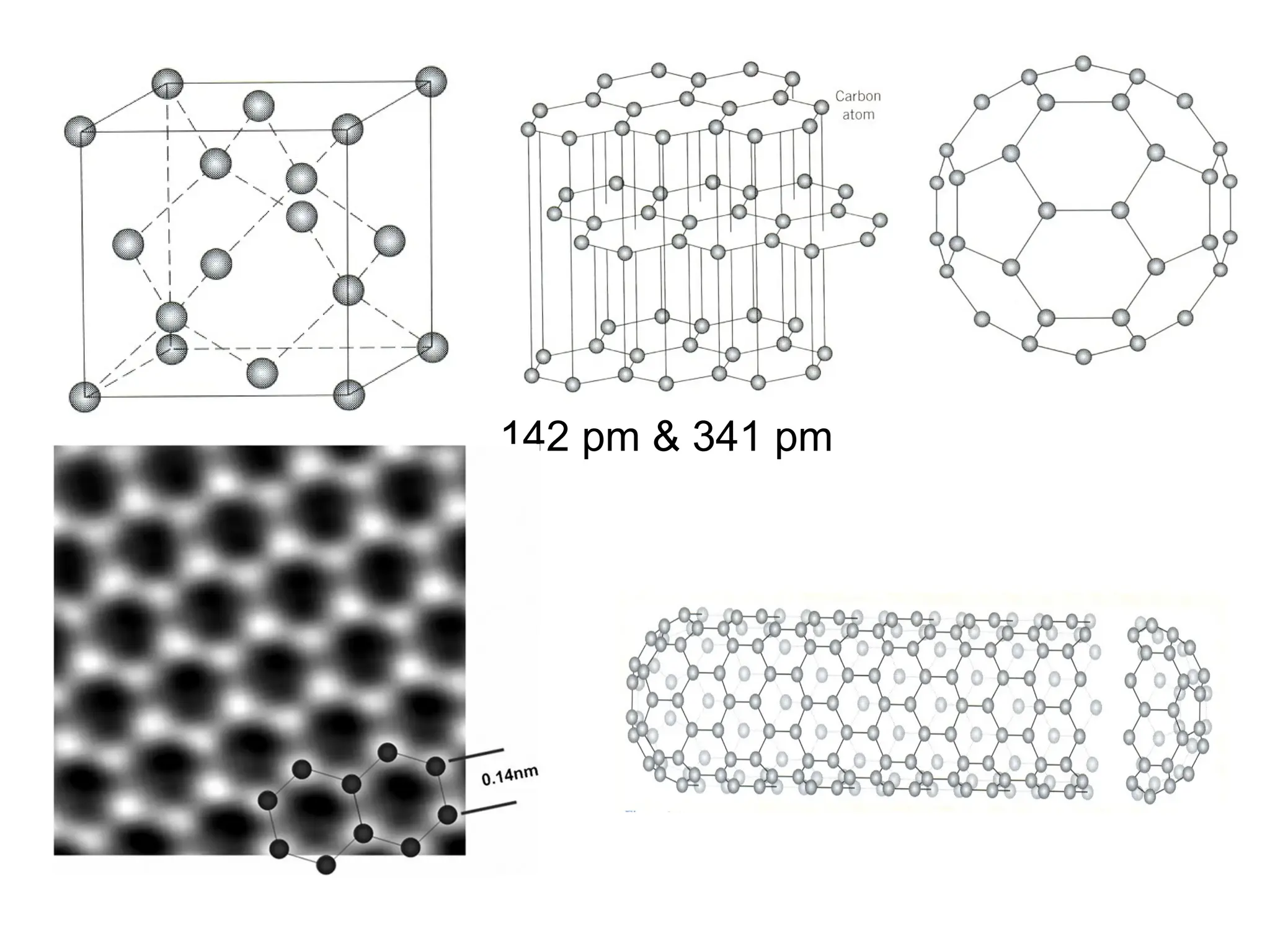
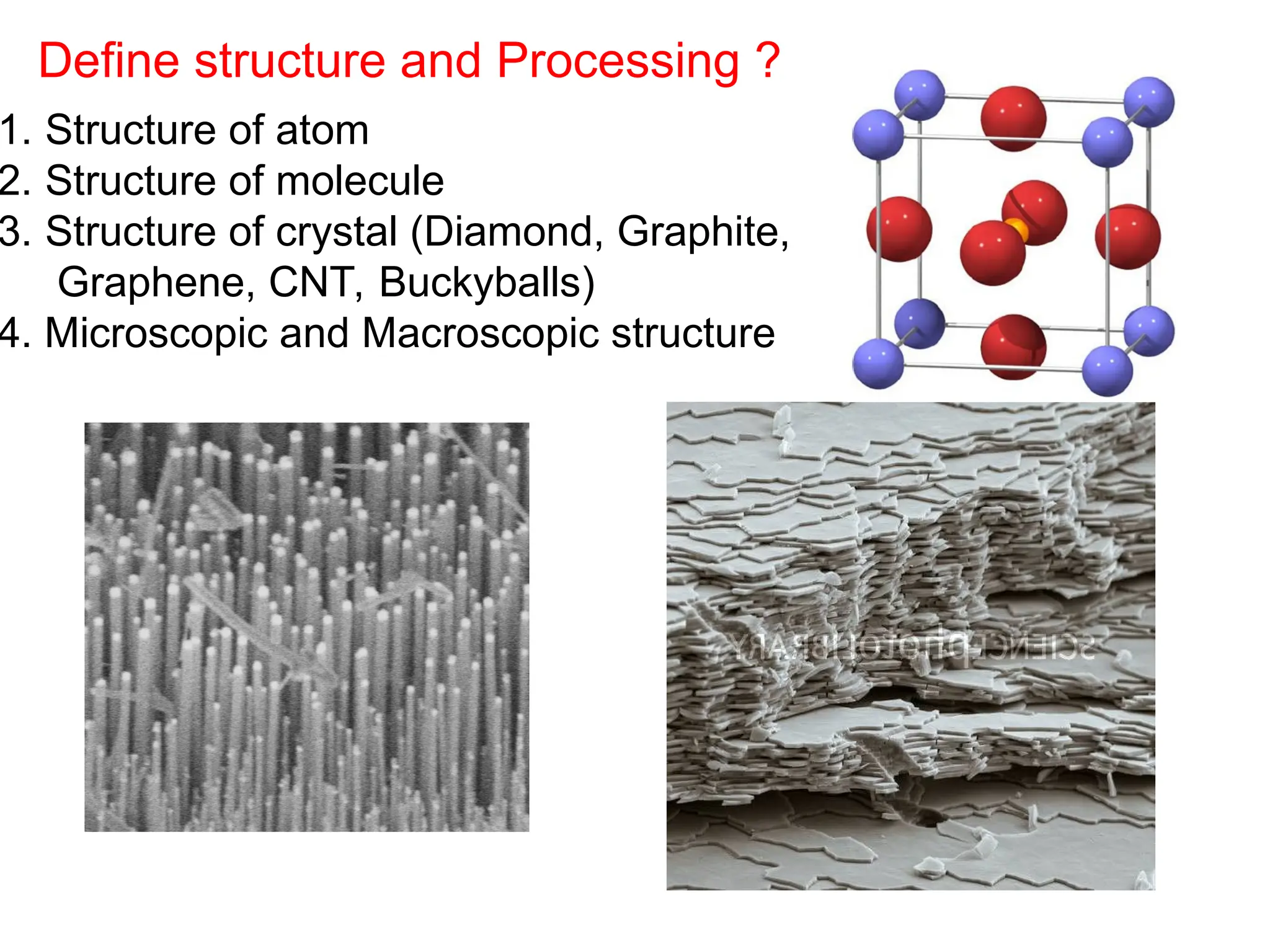
Chapter 3: Eight Lect. Crystal structure
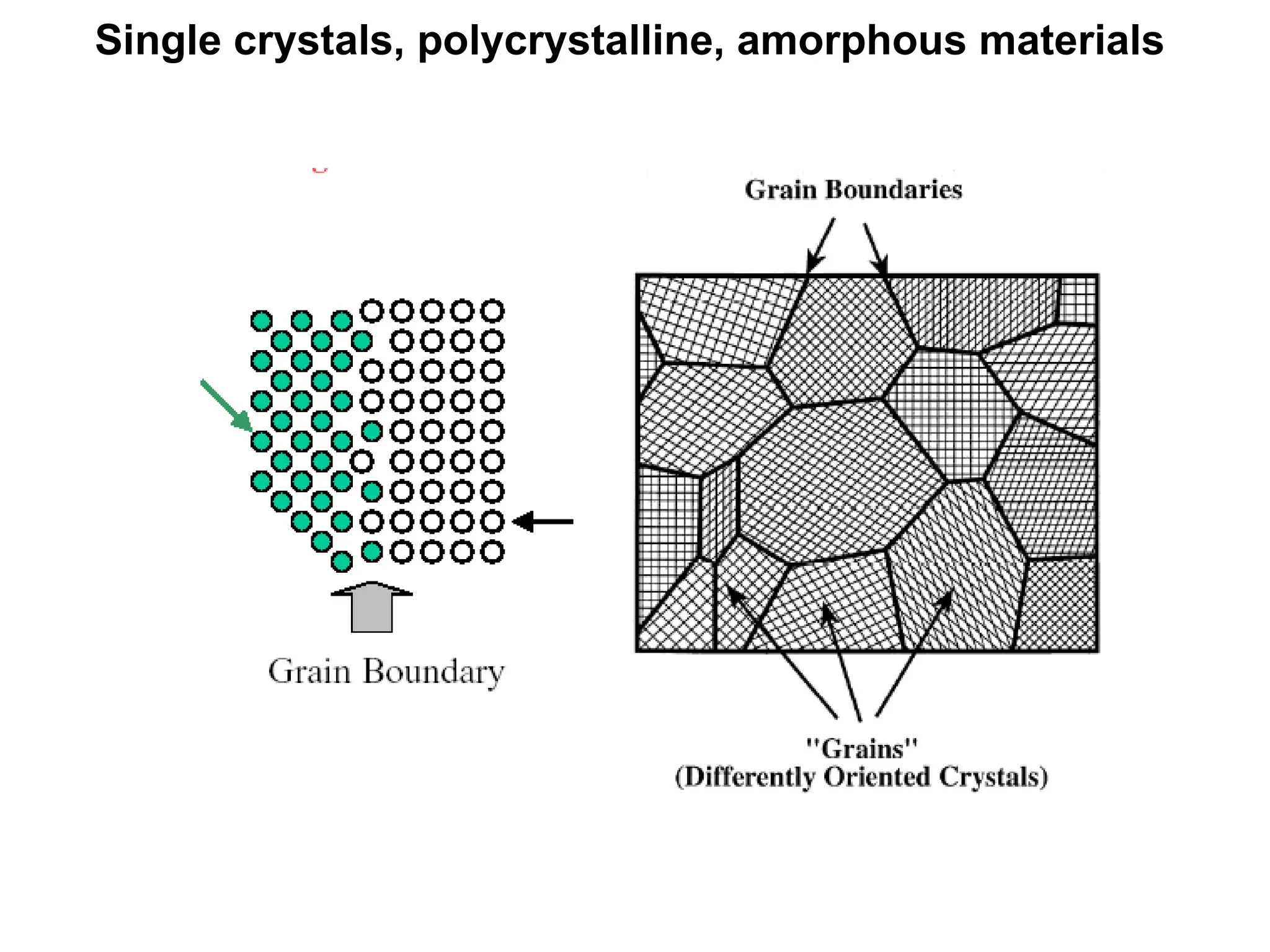
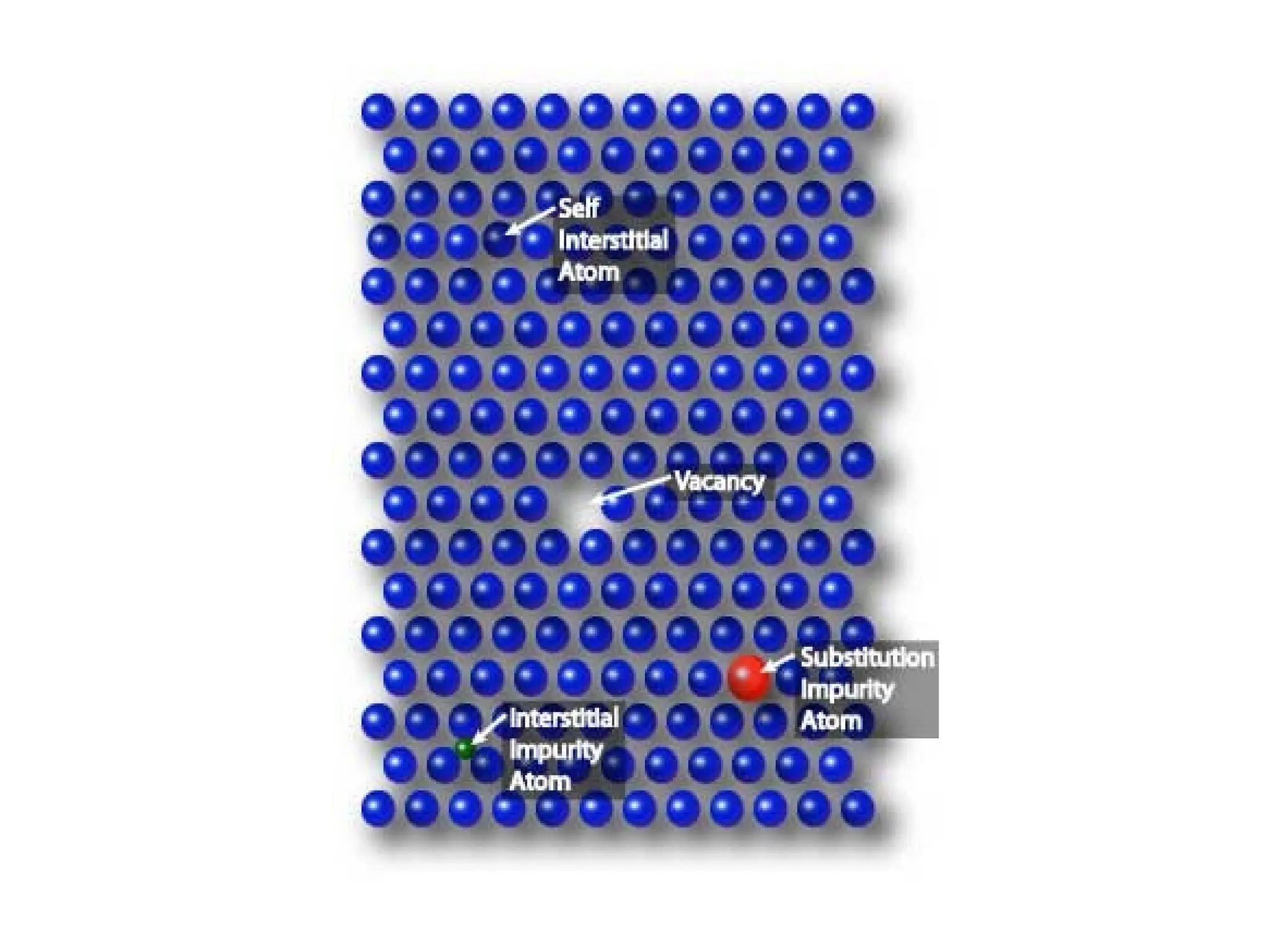
Chapter 4: Five Lect Crystals are imperfect
Chapter 5: Four Lect Diffusion in solids
Chapter 6. Four Lect. Mechanical properties of metals
Chapter 7: Four Dislocations and strengthening
Chapter 8. Three Lect. Failure of metals
Chapter 9: Seven Lect Phase diagrams (Sect 9.13, to 9.17 are not included)
Chapter 10: not included
Chapter 11: Not included Application and processing of metals
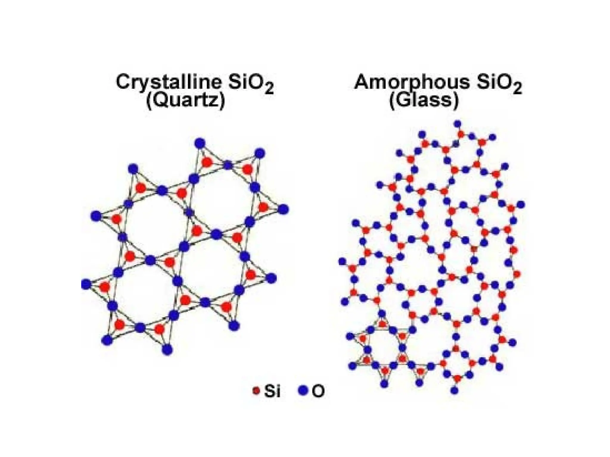
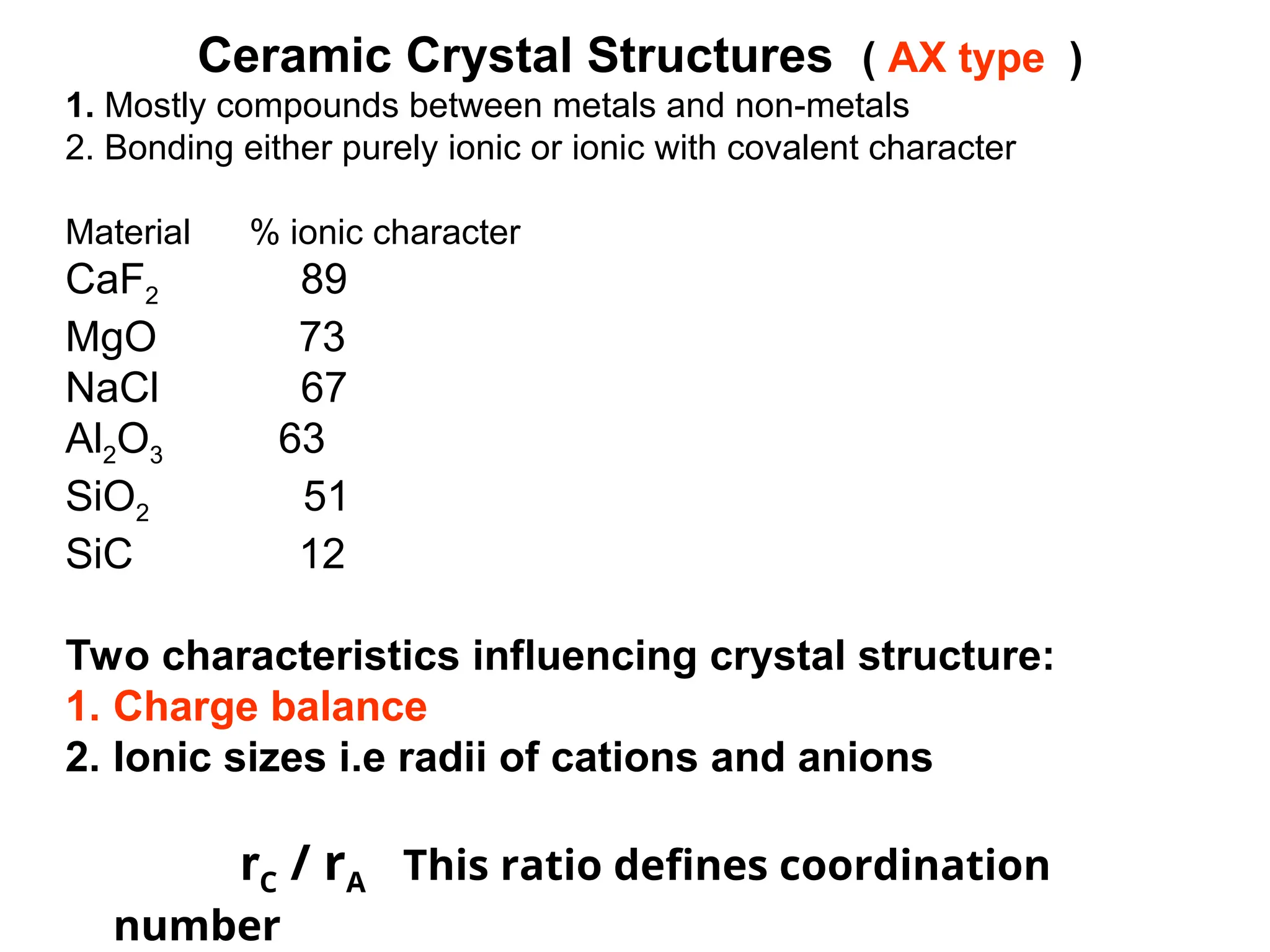
Chapter 12: Three Lect. Ceramics [ Note: Section 12.9 is not included ]
Chapter 13: Not included Application/processing of ceramics
Chapter 14. Three Lect Structure of polymers
Chapter 15: Not included Characterization of polymers
Chapter 16. Two Lect. Composites
Total = 45 Lectures](https://image.slidesharecdn.com/ch-250905070101-91f8f4bf/75/Ch-1-2-3-Spr-19-Material-engineering-ppt-1-2048.jpg)


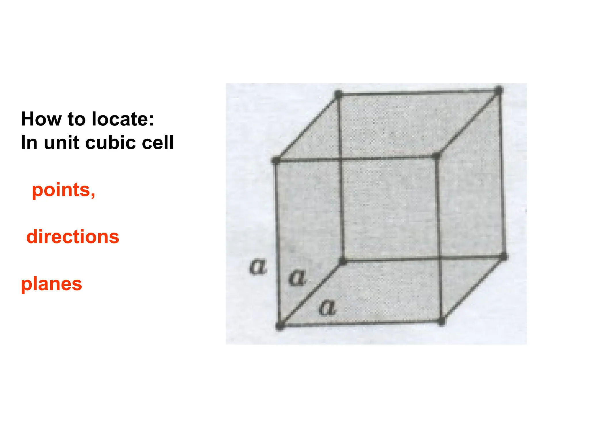
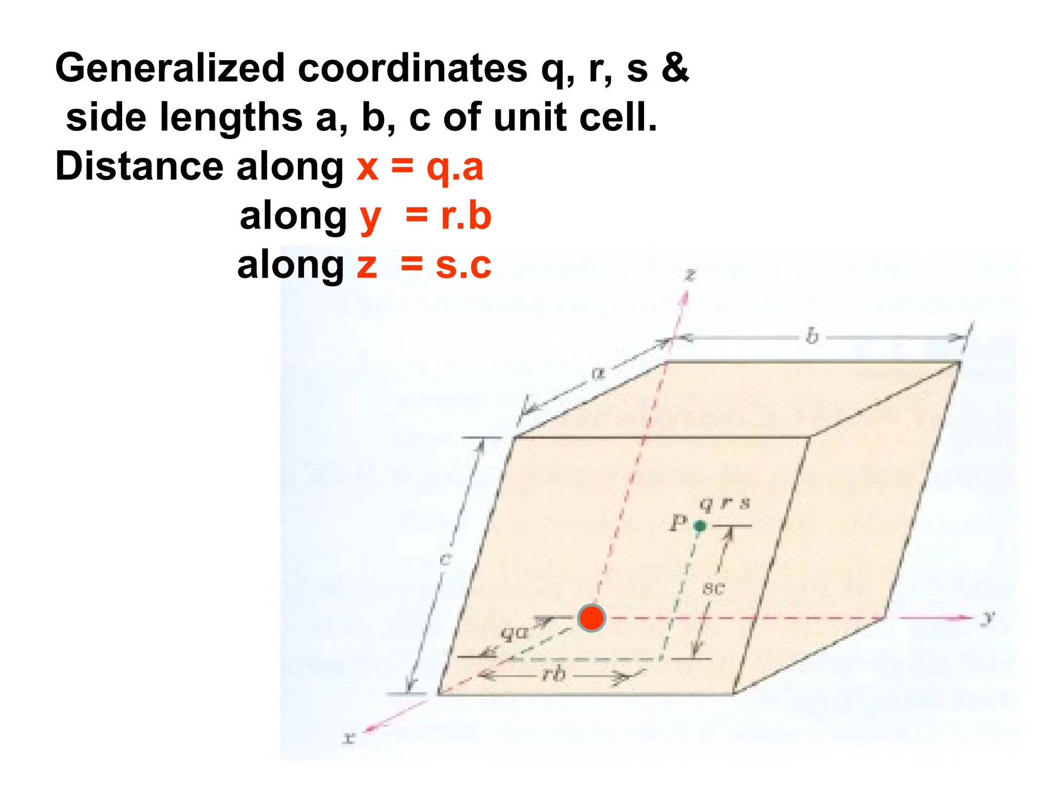
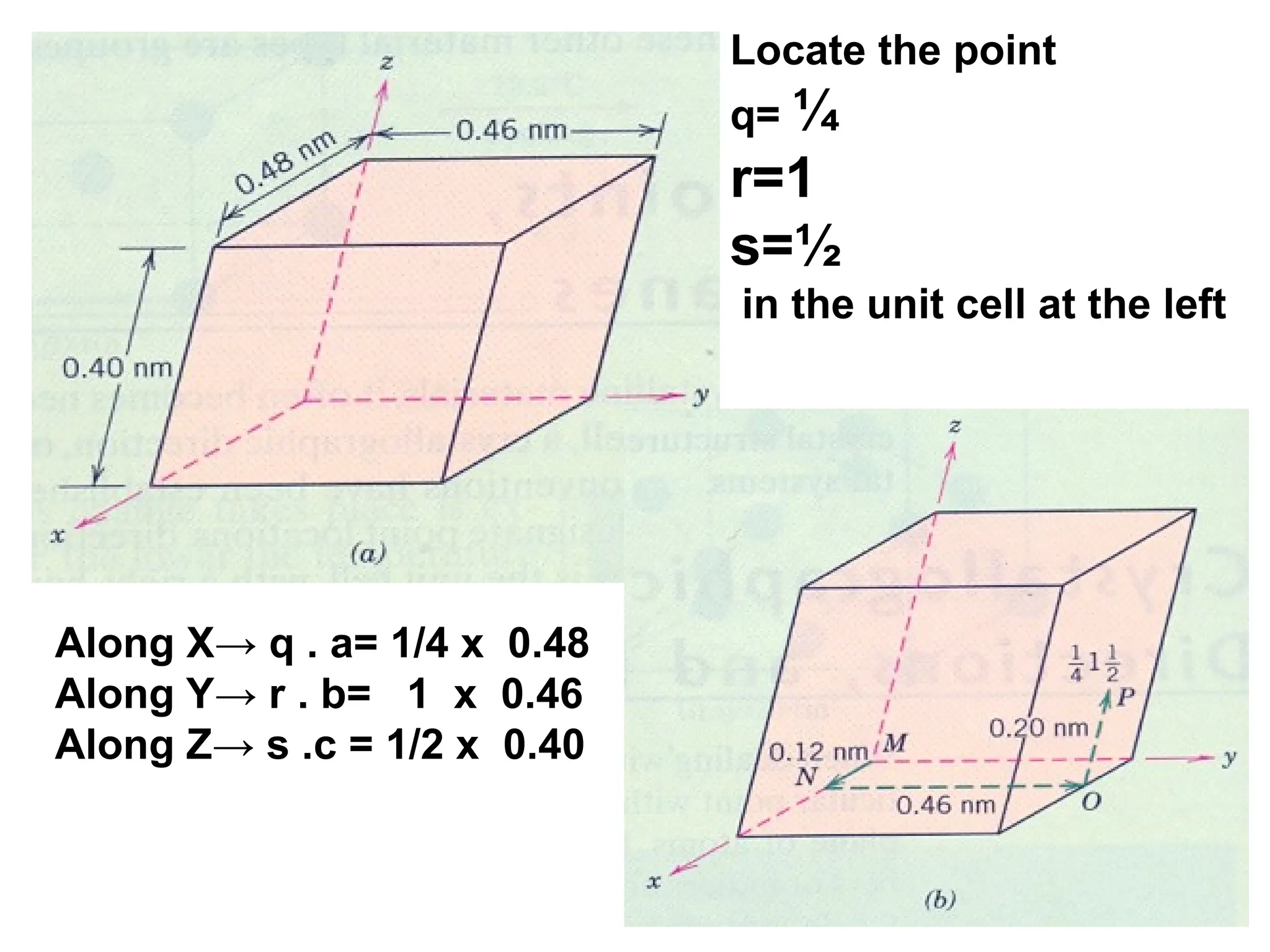
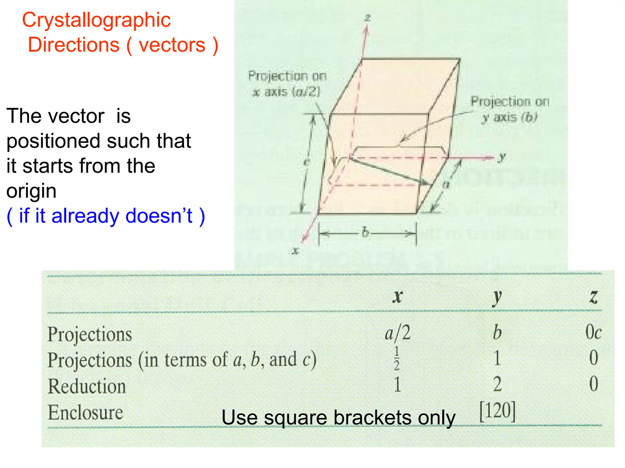
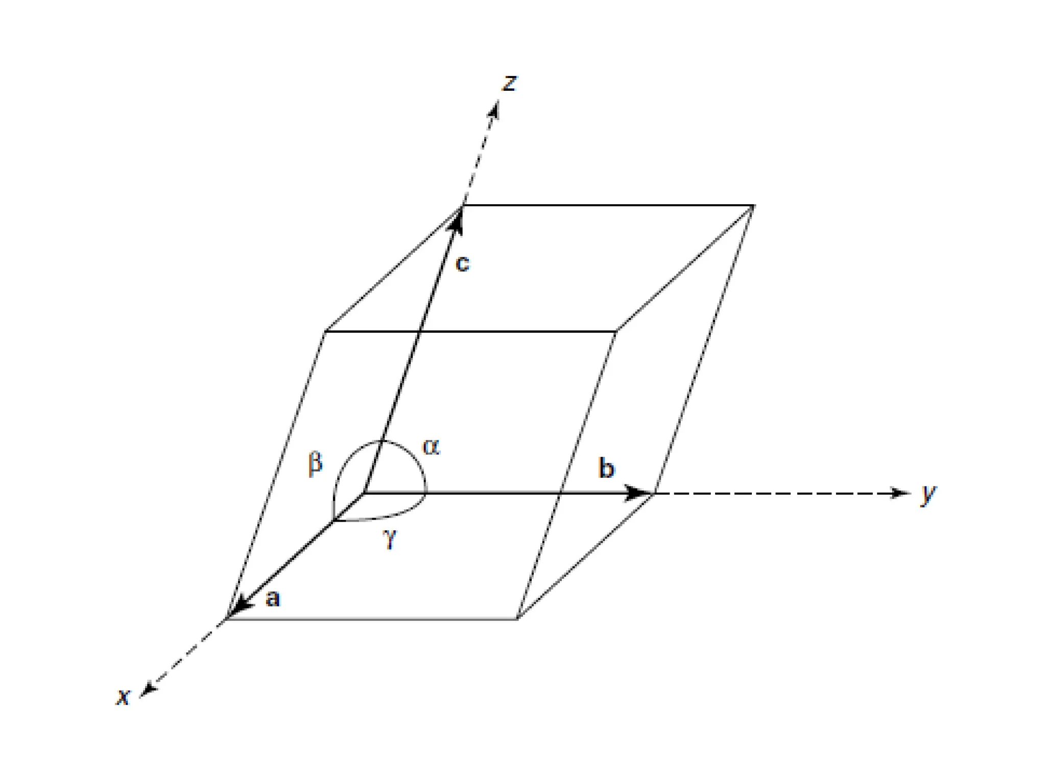
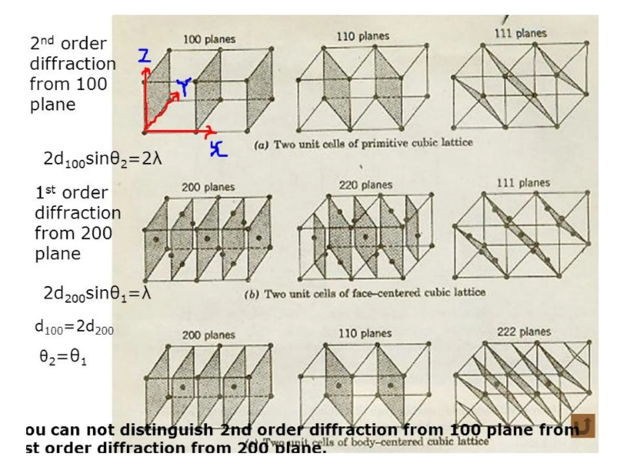
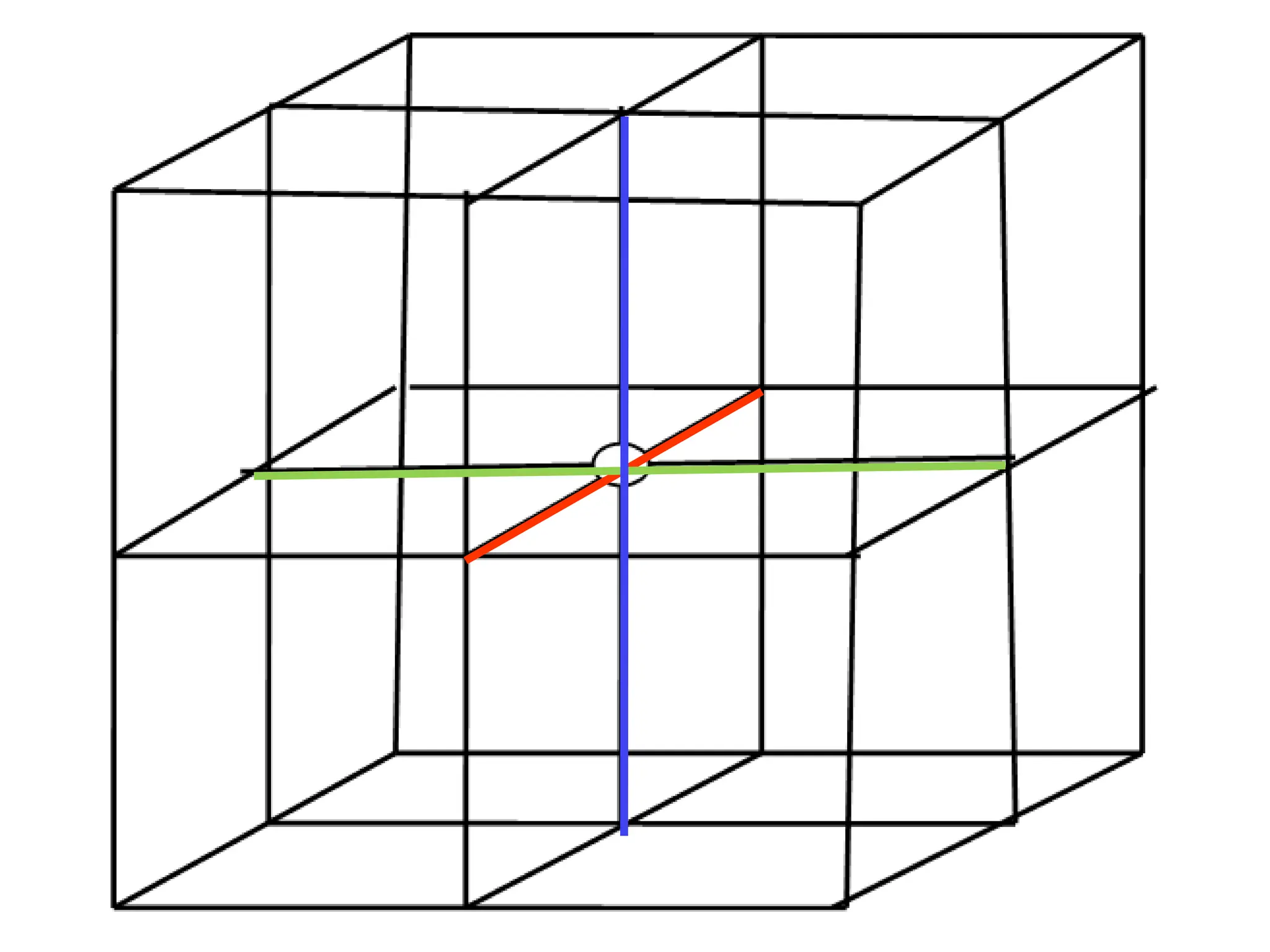
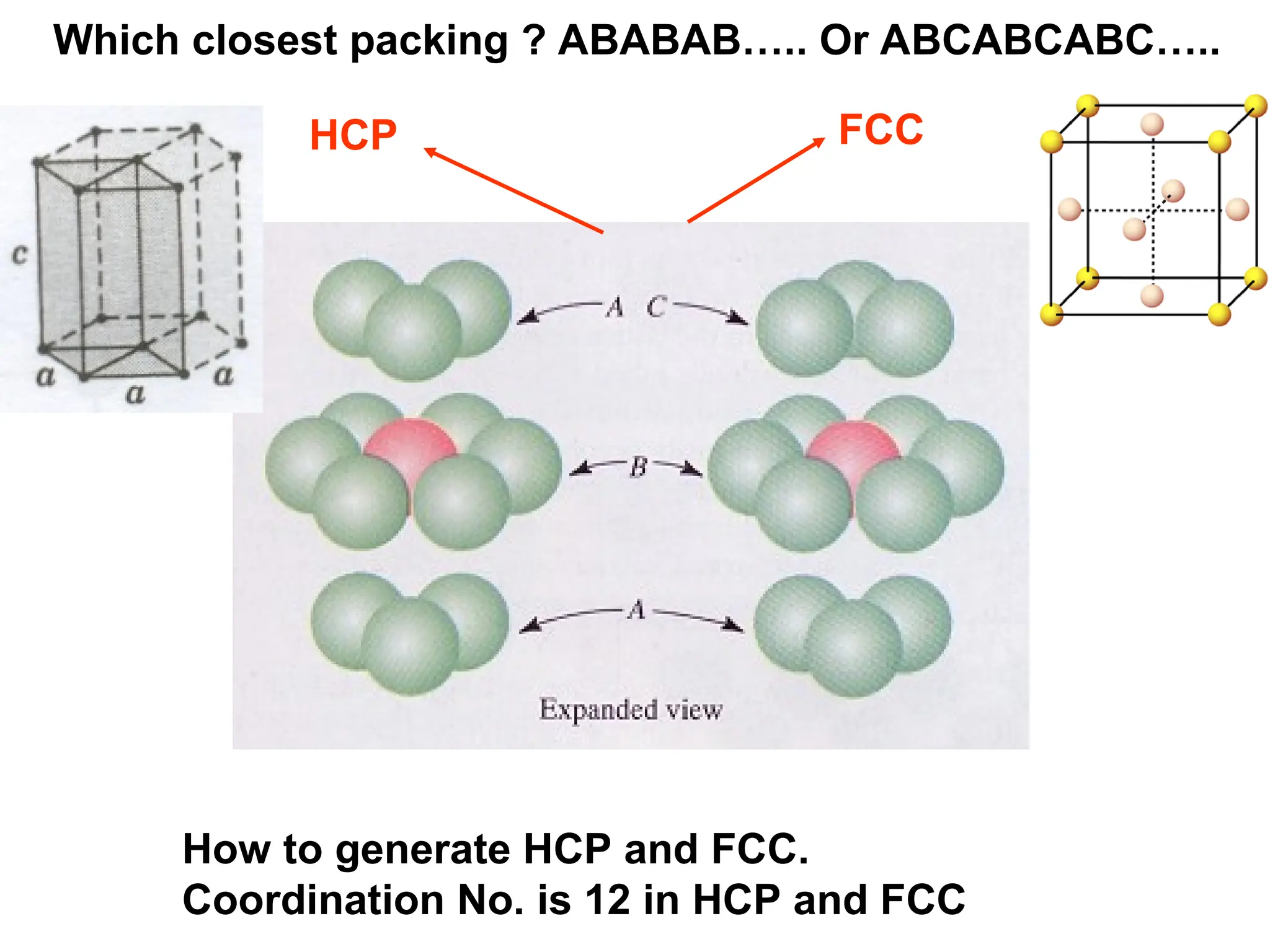
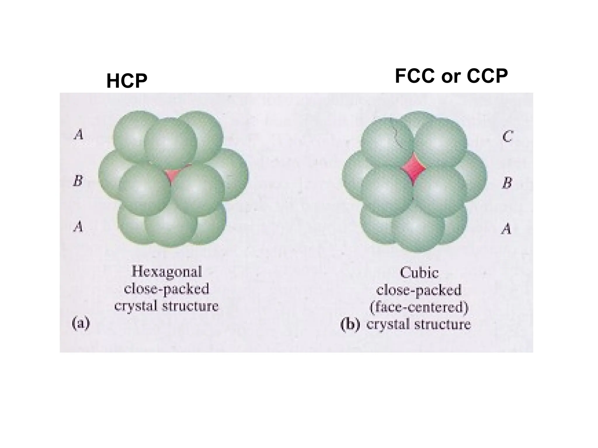
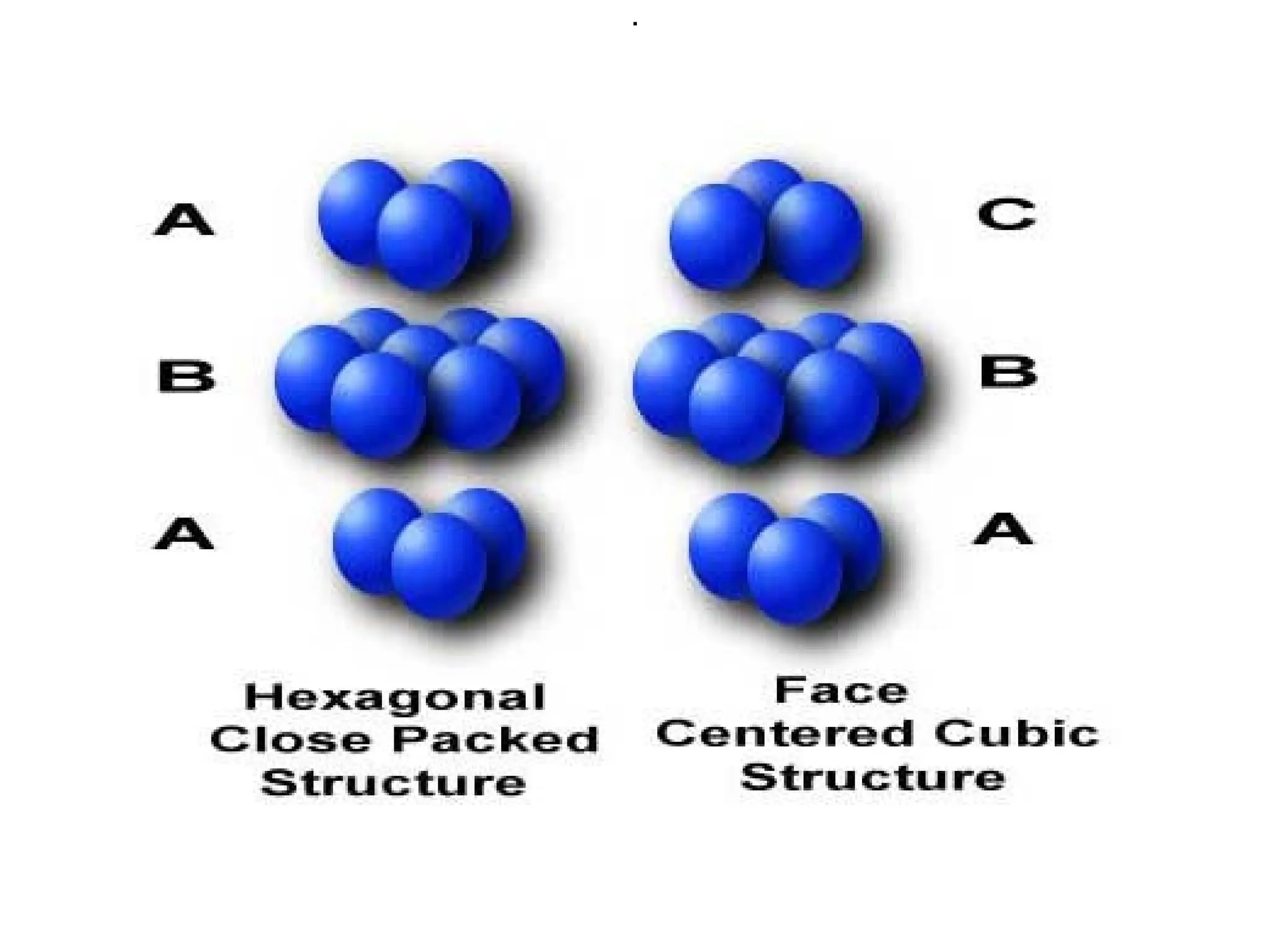
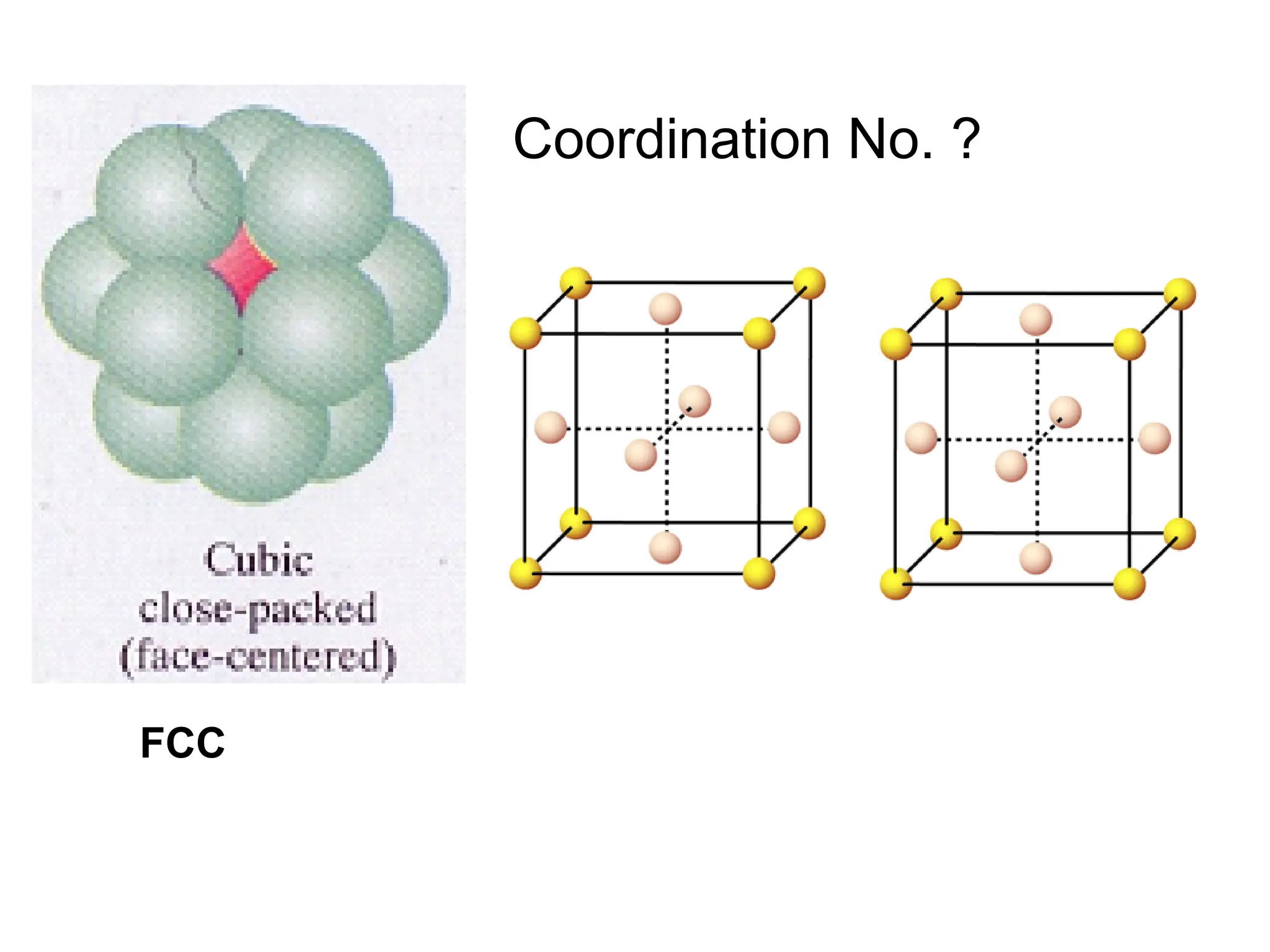
![Crystallographic Directions
1. Position vector through the
origin ( translate if necessary )
2. Measure its projections along
x, y, z & divide by a, b, c
3. Convert values from step 2
into smallest whole numbers
4. Write whole numbers from
step 3 as [uvw]](https://image.slidesharecdn.com/ch-250905070101-91f8f4bf/75/Ch-1-2-3-Spr-19-Material-engineering-ppt-36-2048.jpg)
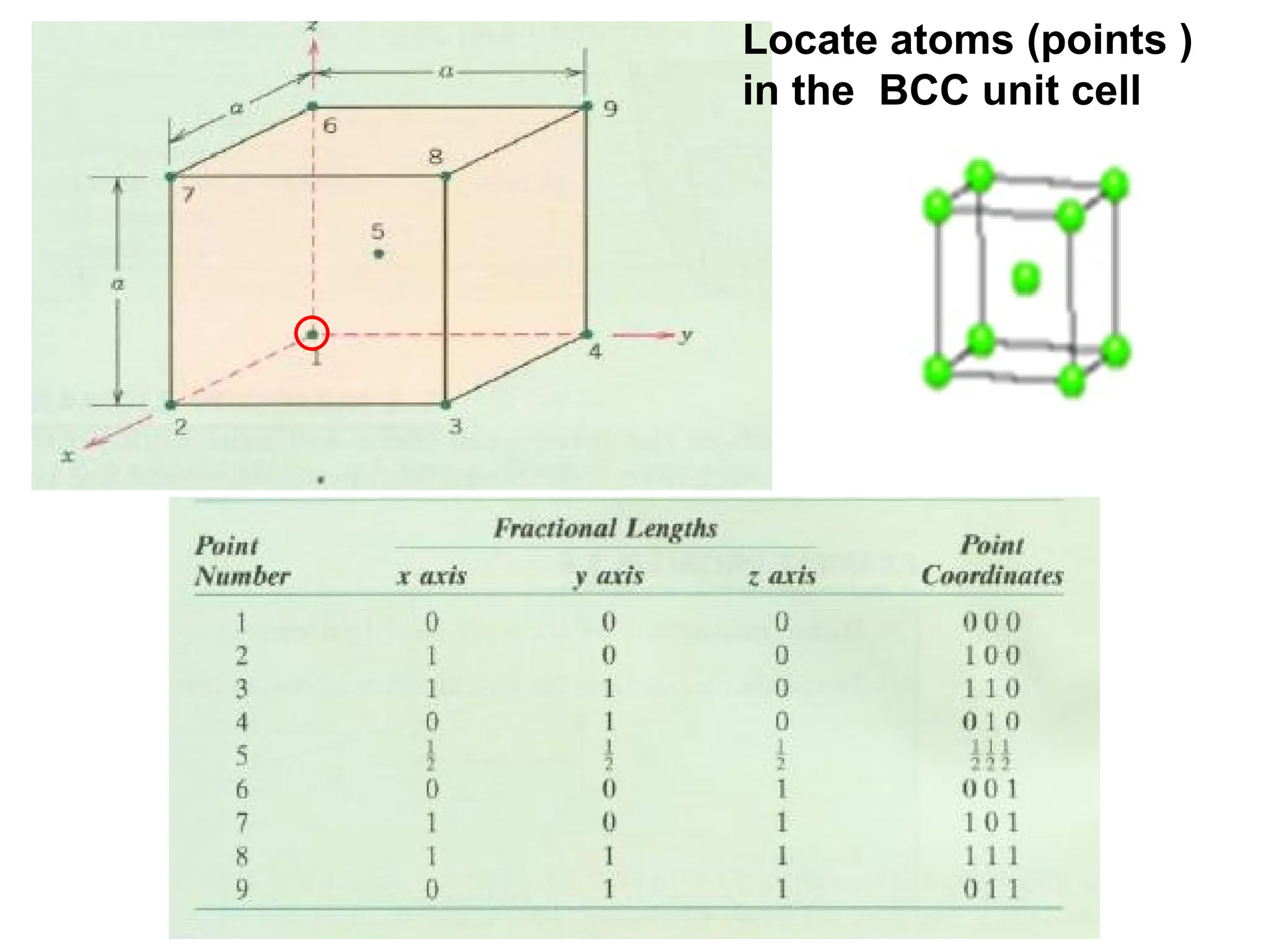
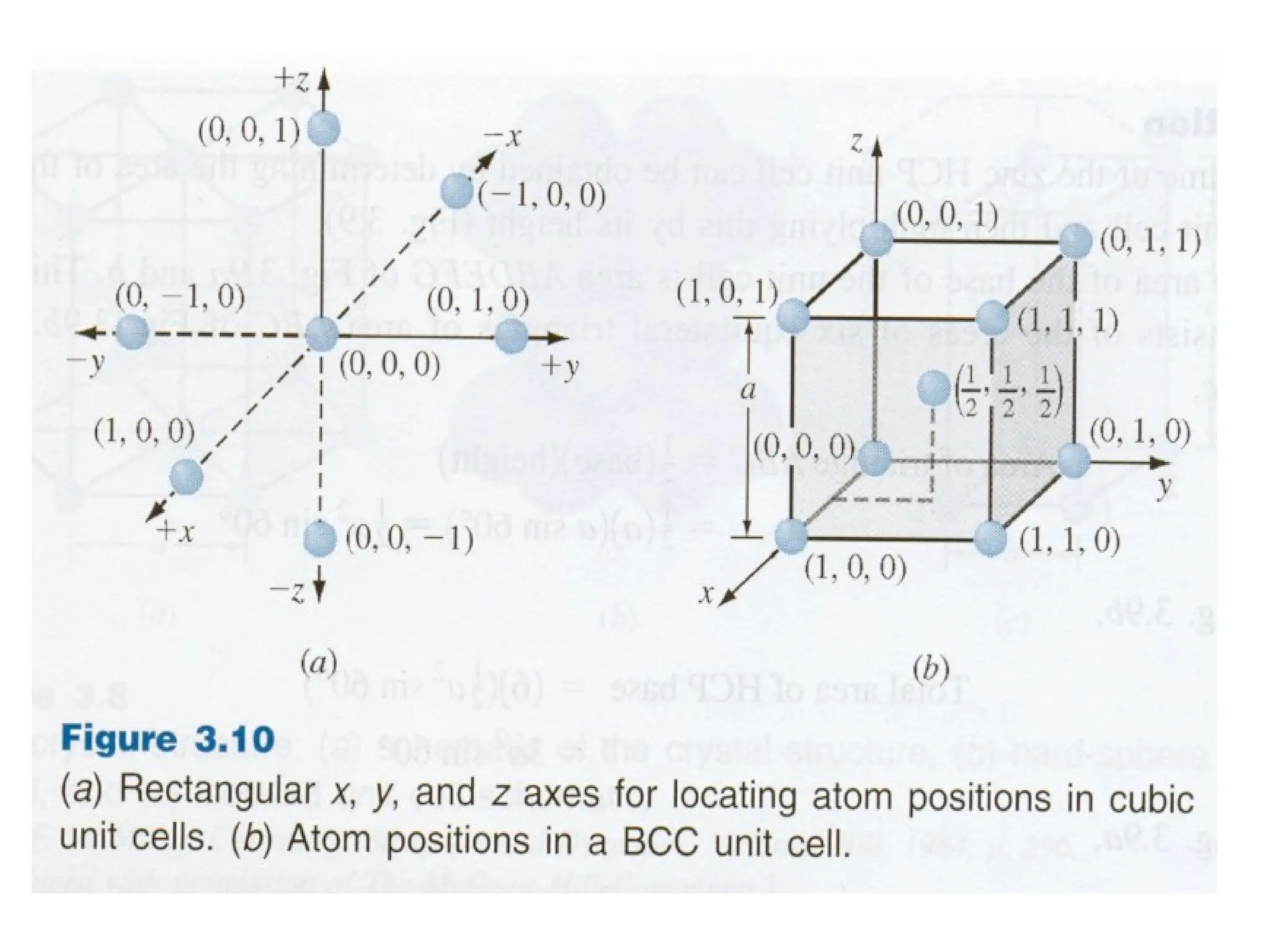
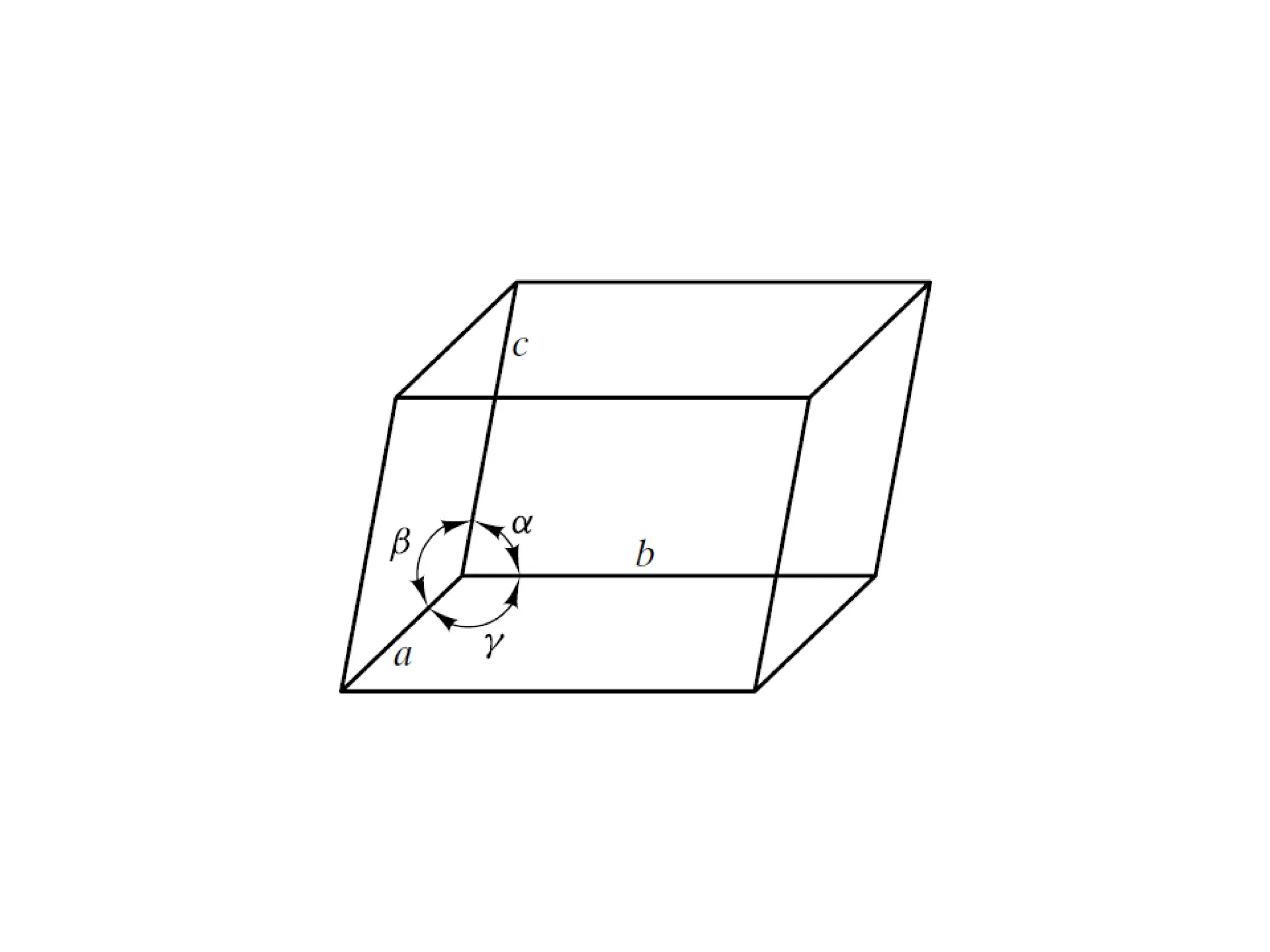
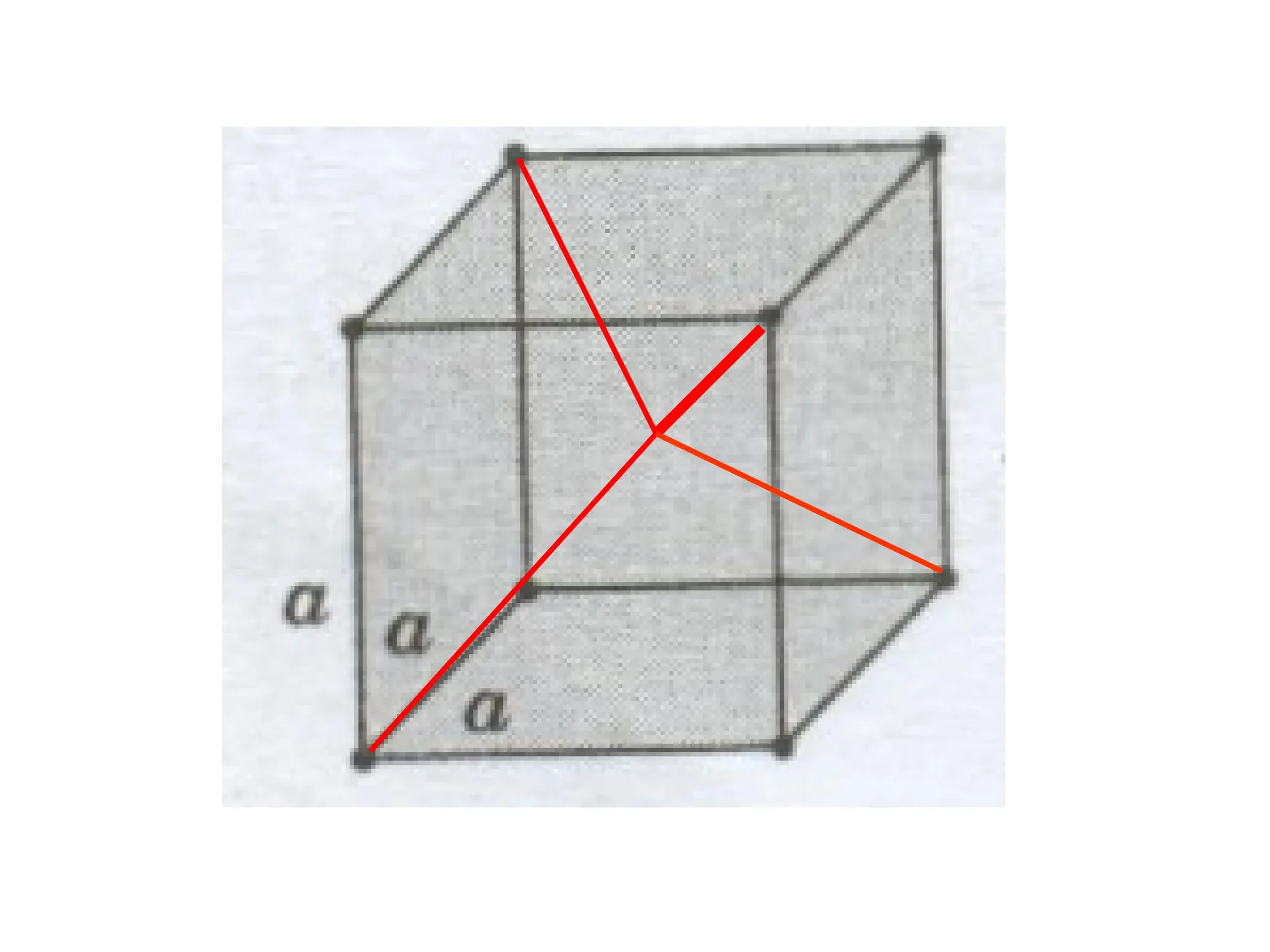
![For cubic Crystals:
Equivalent Directions are defined
[100], [100], [010], [010], [001], [001] are all equivalent directions
because atoms are spaced in the same way.
We write set of equivalent directions as: ‹100›
[123] & [213] →
same indices without regard for
sign or order
are also equivalent](https://image.slidesharecdn.com/ch-250905070101-91f8f4bf/75/Ch-1-2-3-Spr-19-Material-engineering-ppt-38-2048.jpg)
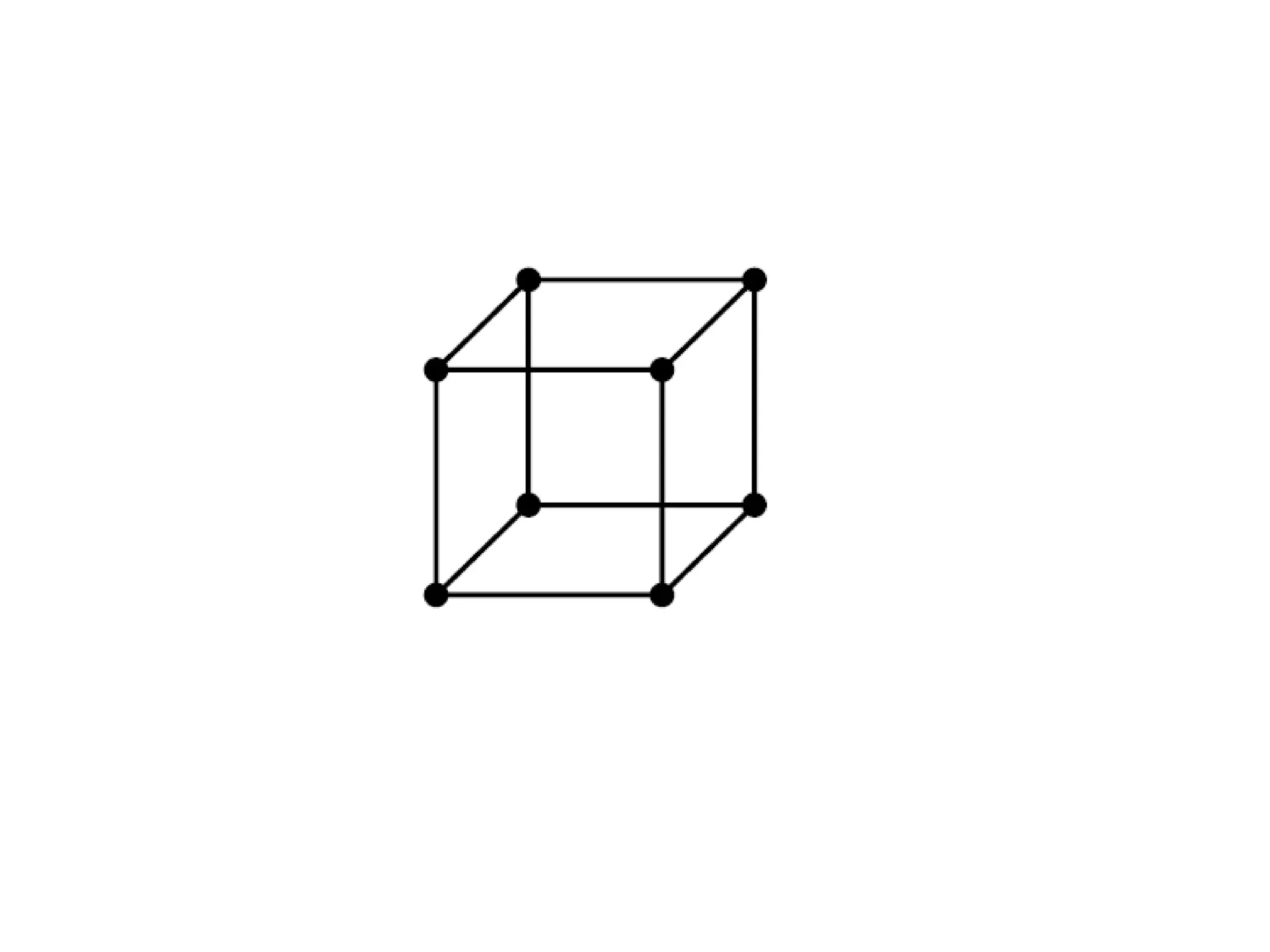
![Show that A is [3 3 1], B is [4 0 3], C is [3 6 1] and D is [1 1 1]](https://image.slidesharecdn.com/ch-250905070101-91f8f4bf/75/Ch-1-2-3-Spr-19-Material-engineering-ppt-41-2048.jpg)
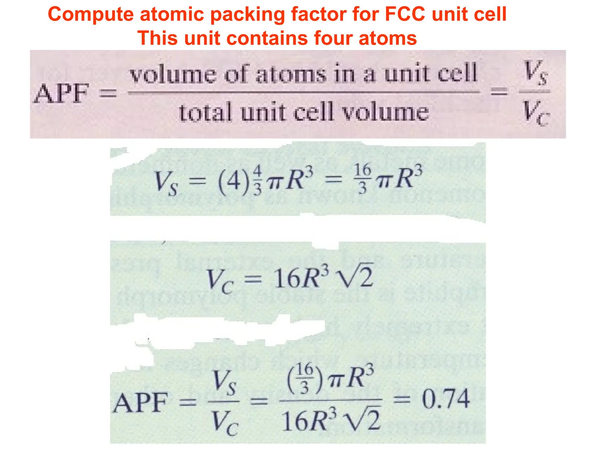
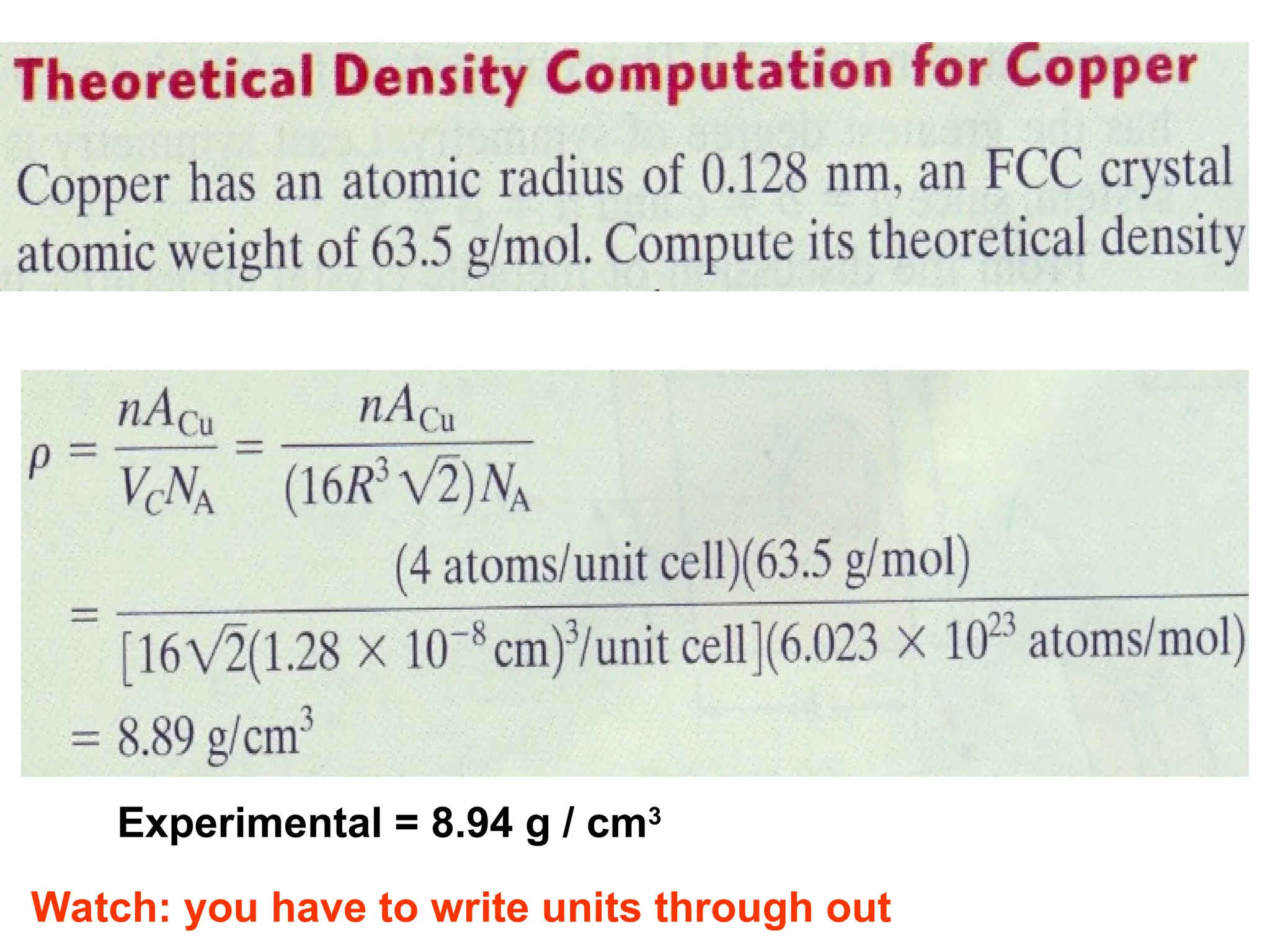

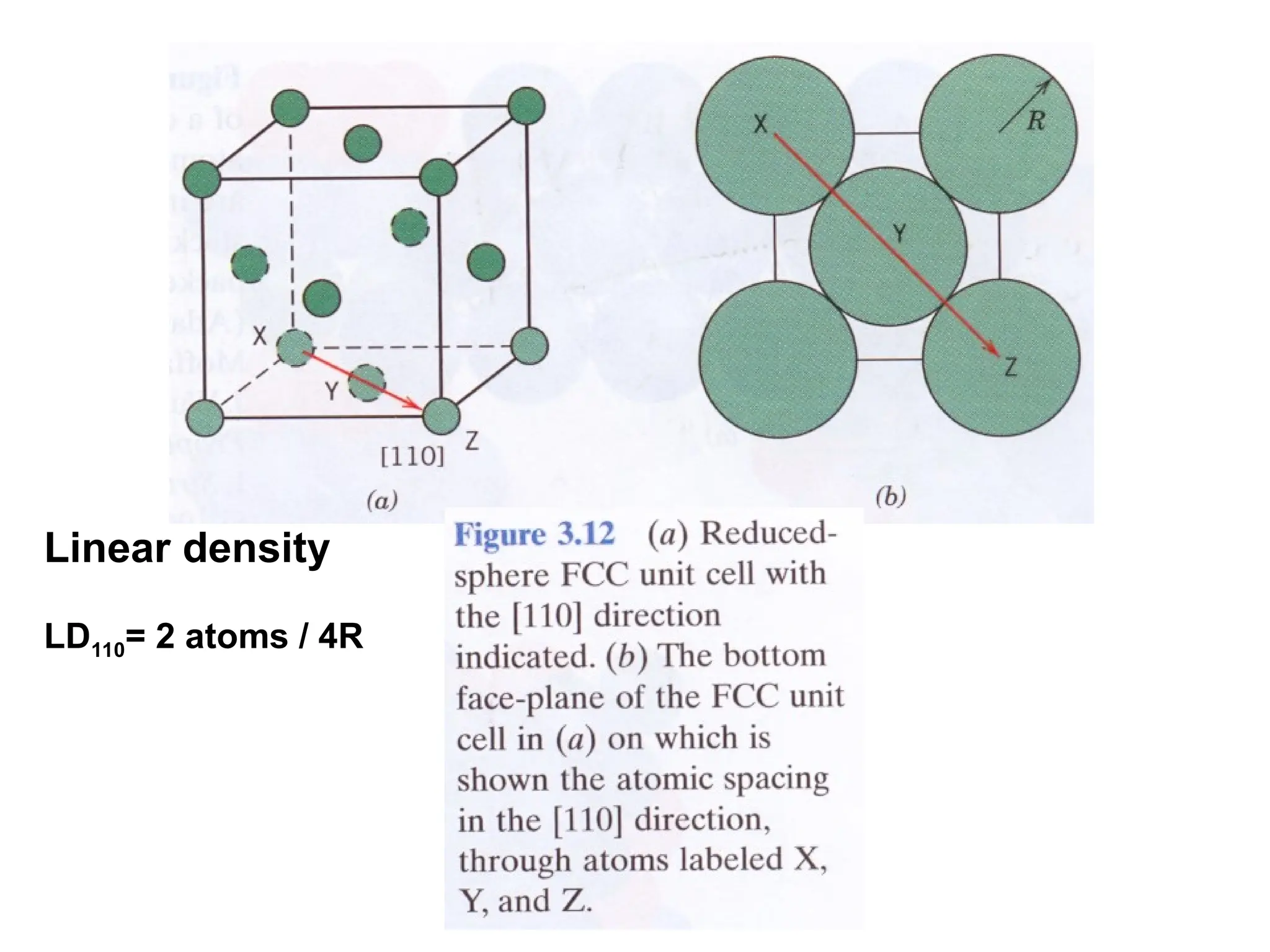
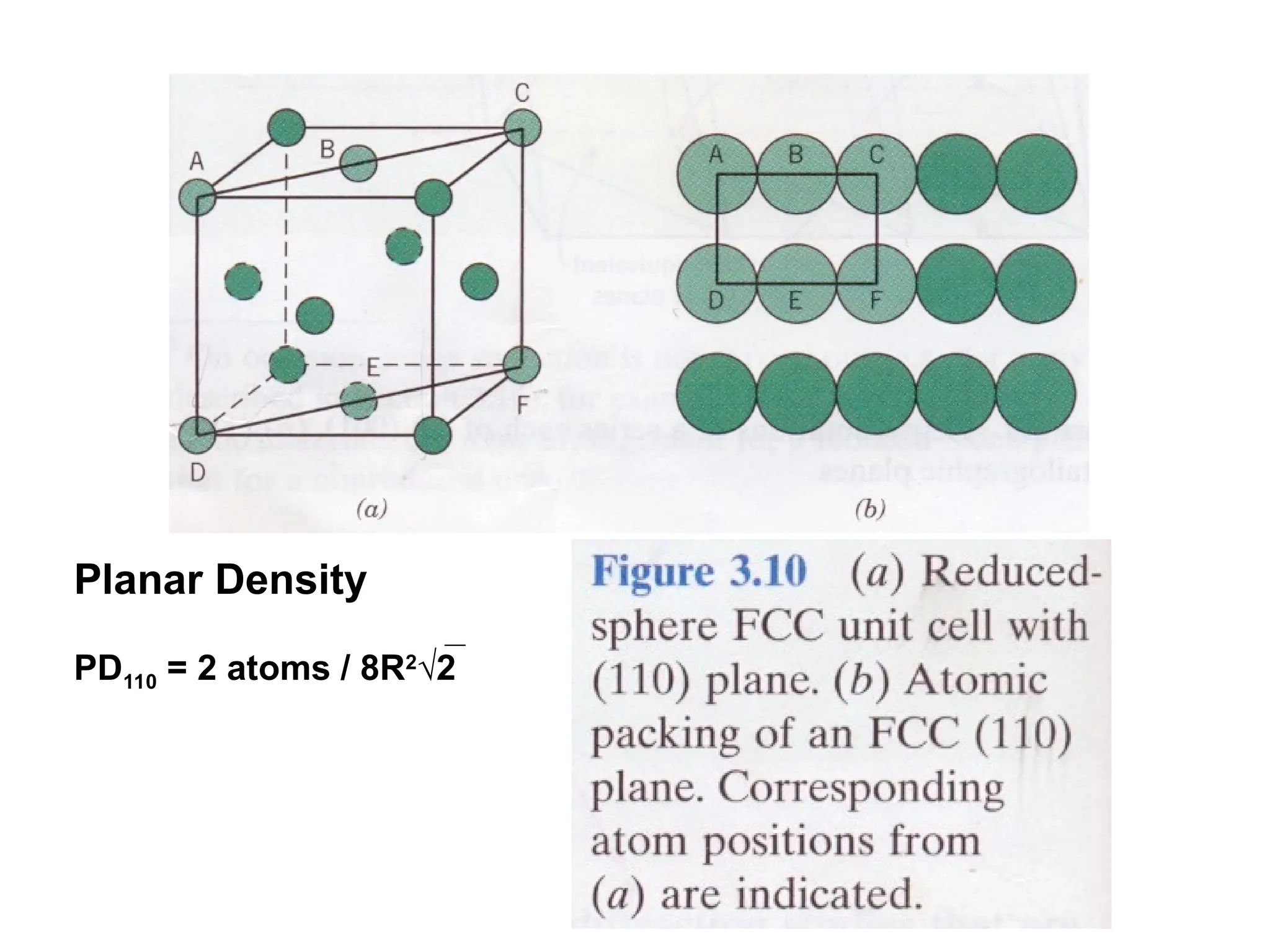
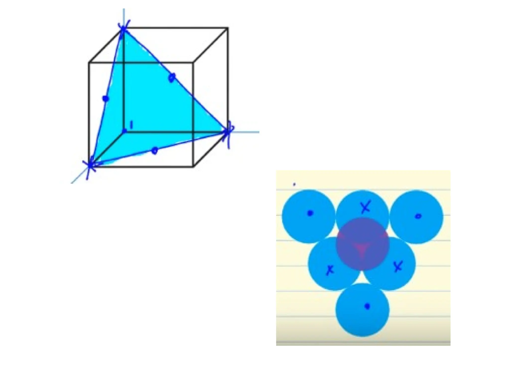
![PD110 =
(2 atoms / [(16√2 R2
)/3]
Area =
Face diagonal x side](https://image.slidesharecdn.com/ch-250905070101-91f8f4bf/75/Ch-1-2-3-Spr-19-Material-engineering-ppt-91-2048.jpg)