Downloaded 128 times


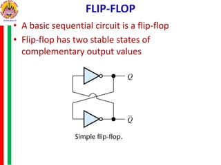

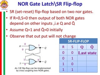
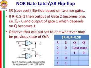
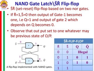
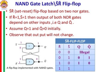
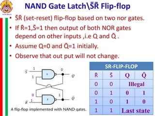
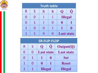
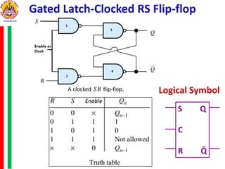

1. A flip-flop is a basic element of sequential circuits that has two stable states and whose output depends on both the current input and its previous state. 2. An SR flip-flop can be constructed using two NOR gates, with states that are set by a high S input and reset by a high R input. 3. Gated flip-flops only change state in response to changes at the clock input, allowing the circuit response to be controlled at specific times.


![16148_flip-flopaaaaaaaaaaaaaaaaa1[1].ppt](https://cdn.slidesharecdn.com/ss_thumbnails/16148flip-flop11-241007142703-8f186e77-thumbnail.jpg?width=640&height=640&fit=bounds)


