INTERFACING WITH INTEL 8251A (USART)

The Read/Write Control logic interfaces the 8251A with CPU, determines the functions of the 8251A according to the control word written into its control register. It monitors the data flow. This section has three registers and they are control register, status register and data buffer. The active low signals RD, WR, CS and C/D(Low) are used for read/write operations with these three registers. When C/D(low) is high, the control register is selected for writing control word or reading status word. When C/D(low) is low, the data buffer is selected for read/write operation. When the reset is high, it forces 8251A into the idle mode. The clock input is necessary for 8251A for communication with CPU and this clock does not control either the serial transmission or the reception rate.ThesisScientist.com

Recommended
More Related Content
What's hot
What's hot (20)
Similar to INTERFACING WITH INTEL 8251A (USART)
Similar to INTERFACING WITH INTEL 8251A (USART) (20)
More from Prof Ansari
More from Prof Ansari (20)
Recently uploaded
Recently uploaded (20)
INTERFACING WITH INTEL 8251A (USART)
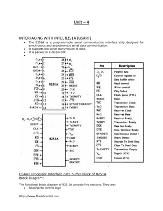
- 1. Https://www.ThesisScientist.com Unit – 4 INTERFACING WITH INTEL 8251A (USART) The 8251A is a programmable serial communication interface chip designed for synchronous and asynchronous serial data communication. It supports the serial transmission of data. It is packed in a 28 pin DIP. USART Processor Interface data buffer block of 8251A Block Diagram: The functional block diagram of 825 1A consists five sections. They are: Read/Write control logic
- 2. Https://www.ThesisScientist.com Transmitter Receiver Data bus buffer Modem control. The functional block diagram is shown in fig: Func tional block diagram of 8251A-USART Read/Write control logic: The Read/Write Control logic interfaces the 8251A with CPU, determines the functions of the 8251A according to the control word written into its control register. It monitors the data flow. This section has three registers and they are control register, status register and data buffer. The active low signals RD, WR, CS and C/D(Low) are used for read/write operations with these three registers. When C/D(low) is high, the control register is selected for writing control word or reading status word. When C/D(low) is low, the data buffer is selected for read/write operation. When the reset is high, it forces 8251A into the idle mode. The clock input is necessary for 8251A for communication with CPU and this clock does not control either the serial transmission or the reception rate. Transmitter section:
- 3. Https://www.ThesisScientist.com The transmitter section accepts parallel data from CPU and converts them into serial data. The transmitter section is double buffered, i.e., it has a buffer register to hold an 8- bit parallel data and another register called output register to convert the parallel data into serial bits. When output register is empty, the data is transferred from buffer to output register. Now the processor can again load another data in buffer register. If buffer register is empty, then TxRDY is goes to high. If output register is empty then TxEMPTY goes to high. The clock signal, TxC (low) controls the rate at which the bits are transmitted by the USART. The clock frequency can be 1,16 or 64 times the baud rate. Receiver Section: The receiver section accepts serial data and convert them into parallel data The receiver section is double buffered, i.e., it has an input register to receive serial data and convert to parallel, and a buffer register to hold the parallel data. When the RxD line goes low, the control logic assumes it as a START bit, waits for half a bit time and samples the line again. If the line is still low, then the input register accepts the following bits, forms a character and loads it into the buffer register. The CPU reads the parallel data from the buffer register. When the input register loads a parallel data to buffer register, the RxRDY line goes high. The clock signal RxC (low) controls the rate at which bits are received by the USART. During asynchronous mode, the signal SYNDET/BRKDET will indicate the break in the data transmission. During synchronous mode, the signal SYNDET/BRKDET will indicate the reception of synchronous character. MODEM Control: The MODEM control unit allows to interface a MODEM to 8251A and to establish data communication through MODEM over telephone lines. This unit takes care of handshake signals for MODEM interface. The 825 1A can be either memory mapped or I/O mapped in the system. 8251A in I/O mapped in the system is shown in the figure. Using a 3-to-8 decoder generates the chip select signals for I/O mapped devices. The address lines A4, A5 and A6 are decoded to generate eight chip select signals (IOCS-0 to IOCS-7) and in this, the chip select signal IOCS-2 is used to select 8251A. The address line A7 and the control signal IO / M(low) are used as enable for decoder. The address line A0 of 8085 is connected to C/D(low) of 8251A to provide the internal addresses. The data lines D0 - D7 are connected to D0 - D7 of the processor to achieve parallel data transfer. The RESET and clock signals are supplied by the processor. Here the processor clock is directly connected to 8251A. This clock controls the parallel data transfer between the processor and 8251A.
- 4. Https://www.ThesisScientist.com The output clock signal of 8085 is divided by suitable clock dividers like programmable timer 8254 and then used as clock for serial transmission and reception. The TTL logic levels of the serial data lines and the control signals necessary for serial transmission and reception are converted to RS232 logic levels using MAX232 and then terminated on a standard 9-pin D-.type connector. In 8251A the transmission and reception baud rates can be different or same. The device which requires serial communication with processor can be connected to this 9-pin D-type connector using 9-core cable The signals TxEMPTY, TxRDY and RxRDY can be used as interrupt signals to initiate interrupt driven data transfer scheme between processor and 8251 A. I/O addresses of 8251A interfaced to 8085 is, Control Logic of USART
- 5. Https://www.ThesisScientist.com USART chip (fig. 7-18) is composed of logic circuits, which are connected by an internal data bus. The logic circuits are read/write control logic, modem control, data bus buffer, transmit buffer, transmit control, receive buffer, and receive control. The CPU communicates with the USART over an 8-bit bidirectional tristate data bus. The USART is programmable, meaning the CPU can control its mode of operation using data bus control and command words. The read/write control logic then controls the operation of the USART as it performs specific asynchronous interfacing. READ/WRITE CONTROL. —The read/write control logic accepts control signals from the control bus and command or control words from the data bus. The USART is set to an idle state by the RESET signal or control word. When the USART is IDLE, a new set of control words is required to program it for the applicable interface. The read/write control logic receives a clock signal (CLK) that is used to generate internal device timing. Four control signals are used to govern the read/write operations of the data bus buffer. They are as follows: The CHIP SELECT (CS) signal, when true, enables the USART for reading/writing operations. The WRITE DATA (WD) signal, when true, indicates the microprocessor is placing data or control words on the data bus to the USART. The READ DATA (RD) signal, when true, indicates the microprocessor is ready to receive data or status words from the USART. The CONTROL/DATA (C/D) signal identifies the write operation transfer as data or control words, or the read operation transfer as data or status words. MODEM CONTROL. —The modem control logic generates or receives four control or status signals used to simplify modem interfaces. They are as follows: Figure 7-18.—Universal synchronous/asynchronous receiver transmitter (USART). USART Processor
- 6. Https://www.ThesisScientist.com The USART is a full-duplex synchronous/asynchronous receiver-transmitter proven in high- volume devices from National Semiconductor and available exclusively from IPextreme as synthesizable IP. The USART supports a wide range of software programmable baud rates and data formats and operates in either Synchronous or Asynchronous (UART) mode. It implements automatic parity generation and several error detection schemes. The USART is capable of detecting a wakeup pattern to selectively enable the receiver and implements flow control logic for hardware handshaking. The host interface of the USART complies with the AMBA 2.0 APB protocol. Control registers within the USART provide CPU control of baud rate, frame format, wakeup pattern detection, operating mode, and enabling/disabling interrupts. Status registers provide interrupt and error status. In addition, there are registers that hold the transmit/receive data. In Asynchronous (UART) mode, the USART communicates with other devices using two signals: transmit (TDX) and receive (RDX). In Synchronous mode, the USART communicates with other devices using three signals: transmit (TDX), receive (RDX), and clock (CKX); data bits are transferred synchronously with the CKX signal. Flow control is available in both Asynchronous and Synchronous modes through RTS/CTS signaling. To reduce chip-level pin count, the USART interface signals can be shared with other on-chip functions through a General Purpose I/O (GPIO) Controller. FEATURES Full-duplex double-buffered receiver/transmitter Synchronous operation using the CKX clock pin CKX can be generated internally or externally Asynchronous (UART) operation Programmable baud rate between CLK/2 and CLK/32768 baud
- 7. Https://www.ThesisScientist.com Programmable frame formats o 7, 8, or 9 data bits o 1 or 2 stop bits o Odd, even, mark, space, or no parity Hardware support of parity-bit generation during transmission and parity-bit check during reception Software-controlled break transmission and detection Interrupt on transmit buffer empty, receive buffer full, receive error, and delta clear-to- send (flow control mode) conditions, each with a separate interrupt enable Internal diagnostic capability Automatic error detection o Parity error o Framing error o Data overrun error 9-bit Attention mode DMA support for transmit and receive with separate enables Hardware flow control functions o Clear-to-send (CTS) o Request-to-send (RTS) Wakeup pattern detection according to ISO14230/KWP2000 Debug support: Freeze/suspend USART activity INTERFACES AMBA 2.0 APB host interface o 8-bit read/write data buses o 10-bit address bus USART pins (CKX, TXD, RXD, CTS, RTS) through chip I/O pads (optionally through a GPIO Controller) DMA interface o One transmit DMA channel o One receive DMA channel Clock interface o APB clock for registers, DMA, interrupt functions, and for baud rate generation in Asynchronous mode o Baud rate clock input for Synchronous mode with external baud rate generation o Baud rate clock output for Synchronous mode with internal baud rate generation Interrupt interface (four interrupts) One asynchronous reset input Freeze/suspend interface DFT signals HARDWARE CONFIGURATION OPTIONS OPTION RANGE DEFAULT
- 8. Https://www.ThesisScientist.com Local clock gating for low- power operation On or Off Off Clock synchronization for FPGA implementation On or Off Off Wakeup detection logic Included or Excluded Excluded GATE COUNT AND PERFORMANCE Gate count and maximum frequency depend on synthesis tool and target technology. Example values for a typical 130-nm technology are: 2300 (NAND2 equivalent) gates 100 MHz (APB clock) MODEMS INTRODUCTION The need to communicate between distant computers led to the use of the existing phone network for data transmission. Most phone lines were designed to transmit analog information - voices, while the computers and their devices work in digital form - pulses. So, in order to use an analog medium, a converter between the two systems is needed. This converter is the MODEM which performs MODulation and DEModulation of transmitted data. It accepts serial binary pulses from a device, modulates some property (amplitude, frequency, or phase) of an analog signal in order to send the signal in an analog medium, and performs the opposite process, enabling the analog information to arrive as digital pulses at the computer or device on the other side of connection. Modems, in the beginning, were used mainly to communicate between DATA TERMINALS and a HOST COMPUTER. Later, the use of modems was extended to communicate between END COMPUTERS. This required more speed and the data rates increased from 300 bps in early days to 28.8bps today. Today, transmission involves data compression techniques which increase the rates, error detection and error correction for more reliability. In order to enable modems of various types and different manufacture to communicate, interface standards were developed by some standard organizations Today's modems are used for different functions. They act as textual and voice mail systems, facsimiles, and are connected or integrated into cellular phones and in notebook computers enabling sending data from anywhere. The future might lead to new applications. Modem speeds are not expected to be increased much over today's 28.8 kbps. Further dramatic speed increases will require digital phone technology such as ISDN and fiber optic lines.
- 9. Https://www.ThesisScientist.com New applications might be implemented such as simultaneous voice and data. Videophones are an example of this. CLASSIFICATION OF MODEMS The modems can be classified according to their characteristics: Range o Short Haul o Voice Grade (VG) o Wideband Line Type o Dial-up o Leased o Private Operation Mode o Half Duplex o Full Duplex o Simplex Synchronization o Asynchronous o Synchronous Modulation o AM o FM/FSK o PM o TCM Data Rate Classifying Modems according to : Range * Short Haul Short haul modems are cheap solutions to systems of short ranges (up to 15 km), which use private lines and are not part of a public system. Short haul modems can also be used, even if the end-to-end length of the direct connection is longer than 15 km, when both ends of the line are served by the same central office in the telephone system. These lines are called "local loops". Short haul modems are distance-sensitive, because signal attenuation occurs as the signal travels through the line. The transmission rate must be lowered to ensure consistent and error-free transmission on longer distances. Short haul modems tend to be cheaper than other modems for two reasons: (1) No circuitry is included in them to correct for differences between the carrier frequency of the demodulator and the frequency of the modulator. (2) Generally no circuitry is included to reduce/correct for noise rejection, which is less of a problem over short distances than over long distances. There are two main types of short haul modems:
- 10. Https://www.ThesisScientist.com 1. Analog modems, using a simple modulation method, without sophisticated devices for error control or equalizers. These modems usually operates at a maximum rate of 9600 bps, but there are some which supports higher rates (up to 64,000 bps). 2. Line drivers increase the digital signal, which transmit to the communication channel and do not transmit the carrier signal, as conventional modems. Line drivers are very cheap and tiny and connect to the RS232 connector of the terminal (since they lack a power supply, they use the signal voltage of the DTE-DCE interface for DC power supply). * Voice Grade (VG) Voice-grade modems are used for unlimited destination, using a moderate to high data rate. These modems are expensive and their maintenance and tuning are sophisticated. Communication channels are leased lines and dial-up. Voice-band telephone network is used for data transmission. A user-to-user connection may be either dedicated or dialed. The links in the connection are the same in the two cases, and the only difference for the user is that for some impairments (particularly attenuation and delay distortion), a dedicated (private or leased) line is guaranteed to meet certain specifications, whereas a dialed connection can only be described statistically. * Wideband Wideband modems are used in large-volume telephone-line multiplexing, dedicated computer- to-computer links. These modems exceed high data rates. Classifying Modems according to : Line Type * Leased, Private Leased, private or dedicated lines (usually 4-wire) are for the exclusive use of "leased-line" modems - either pair (in a simple point-to-point connection) or several (on a multidrop network for a polling or a contention system). If the medium is the telephone network, their transmission characteristics are usually guaranteed to meet certain specifications, but if the link includes any radio transmission, the quality of it may be as variable as that of a switched (i.e. nondedicated) line. * Dial up Dial-up modems can establish point-to-point connections on the PSTN by any combination of manual or automatic dialing or answering. The quality of the circuit is not guaranteed, but all phone companies establish objectives. The links established are almost always 2-wire because 4- wire dialing is tedious and expensive. * Two and Four-Wires Lines A four-wire (4W) line is a pair of two-wire (2W) lines, one for transmitting and one for receiving, in which the signals in the two directions are to be kept totally separate. Perfect separation can be maintained only if the four-wire configuration is sustained from transmitter to receiver. The lines may be combined in a 4W/2W network (often called a hybrid or a hybrid transformer) at any point in the signal path. In this case impedance mismatches will cause reflections and interference between the two signals.
- 11. Https://www.ThesisScientist.com Classifying Modems according to : Operation Mode * Half Duplex Half duplex means that signals can be passed in either direction, but not in both simultaneously. A telephone channel often includes an echo-suppressor, allowing transmission in only one direction, this renders the channel half-duplex. Echo suppressors are slowly being replaced by echo cancelers, which are theoretically full-duplex devices. When a modem is connected to a two-wire line, its output impedance cannot be matched exactly to the input impedance of the line, and some part of its transmitted signal (usually badly distorted) will always be reflected back. For this reason half- duplex receivers are disabled (received data is clamped) when their local transmitter is operative. Half-duplex modems can work in full-duplex mode. * Full Duplex Full duplex means that signals can be passed in either direction, simultaneously. Full duplex operation on a two-wire line requires the ability to separate a receive signal from the reflection of the transmitted signal. This is accomplished by either FDM (frequency division multiplexing) in which the signals in the two directions occupy different frequency bands and are separated by filtering, or by Echo Canceling (EC). The implication of the term full-duplex is usually that the modem can transmit and receive simultaneously at full speed. Modems that provide a low-speed reverse channel are sometimes called split-speed or asymmetric modems. Full duplex modems will not work on half-duplex channels. * Simplex Simplex means that signals can be passed in one direction only. A remote modem for a telemetering system might be simplex and a 2-wire line with a common unidirectional amplifier is simplex. * Echo Suppressor and Echo Canceler At the junction between the local loop, which is usually a 2-wire circuit, and the trunk, which is a 4-wire circuit, echoes can occur. The effect of the echo is that a person speaking on the telephone hears his own words after a short delay. Psychological studies have shown that this is annoying to many people, often making them stutter or become confused. To eliminate the problem of echoes, echo suppressors are installed on lines longer than 2000 km. (On short lines the echoes come back so fast that people cannot detect them). An echo suppressor is a device that detects human speech coming from one end of the connection and suppresses all signals going the other way. The device compares the levels at its two input ports, and if it decides, for example that the other end is talking, it inserts an attenuator in the return (echo) path, and vice versa. Echo suppressors have several properties that are undesirable for data communication. First, they prevent full- duplex data transmission, which would otherwise be possible, even over the 2-wire local loop (by allocating part of the bandwidth to the forward channel and part to the reserve channel). Even if half-duplex transmission is adequate, they are a nuisance because the time required to switch directions can be substantial. Double-talking totally confuses them, and the attenuation may be switched in and out repeatedly. Furthermore, they are designed to reverse upon detecting human speech, not digital data.
- 12. Https://www.ThesisScientist.com To reduce these problems, when echo suppressors detect a specific tone they shut down, and remain shut down as long as the carrier is present (this is an example of inband signaling, where control signals that activate and deactivate internal control functions lie within the band accessible to the user). This disabling is usually done during initial handshaking by one modem transmitting an answer tone in either 2100 Hz (CCITT standard) or 2225 Hz (modems following the old Bell 103 standard). Echo suppressor are slowly being replaced by ECs, which allow a certain amount of double- talking and do not require "capture" time for any one talker to assume control of the connection. Classifying Modems according to : Synchronization * Asynchronous Modems Most of the modems that operate in slow and moderate rates, up to 1800 bps, are asynchronous (using asynchronous data). Asynchronous modems operate in FSK modulation and use two frequencies for transmission and another two for receiving. Asynchronous modems can be connected in different options to the communication media: Using 2-wire or 4-wire interface. Using switched lines or leased lines. Using interface to call unit/automatic answer, when dialing-up. In a 2-wire line, full duplex operation can be achieved by splitting the channel into two sub- channels.l Figure Modem - 1 * Asynchronous data Asynchronous data is not accompanied by any clock, and the transmitting and receiving modems know only the nominal data rate. To prevent slipping of the data relative to the modems' clocks,
- 13. Https://www.ThesisScientist.com this data is always grouped in very short blocks (characters) with framing bits (start and stop bits). The most common code used for this is the seven-bit ASCII code with even parity. * Synchronous Modems Synchronous modems operates in the audio domain, at rates up to 28800 bps in audio lines, used in telephones systems (using synchronous data). The usual modulation methods are the phase modulation and integrated phase and amplitude (at higher rates than 4800 bps). In synchronous modems, equalizers are used, in order to offset the misfit of the telephone lines. These equalizers are inserted in addition to the equalizers that sometimes already exist in the telephone lines. These equalizers can be classified into three main groups: 1. Fixed/statistical equalizer - these equalizers offset the signal according to the average of the known attenuation in each frequency. Tuning the equalizer is sometimes done in the factory and stays fixed, usually they are used to operate at low rates in a dial up line. 2. Manually adjusted equalizer - these equalizers can be tuned to optimal performance to a given line. These equalizers should be re-tuned when the line is replaced and periodically. Specially, it should be tuned frequently when the line is of a low quality and it's parameters are changed frequently. Tuning is done using a button inside the modem (or on the external board). 3. Automatic equalizer - these equalizers are tuned automatically when the connection is established. Depending on the line quality in a specific moment, in a process of about 15ms to 25ms, after the first tuning, the equalizer samples the line continually and adjusts itself to the changed conditions, so the modem operates at each moment under optimal conditions. The fitness process operates, in some modems, at rates of 2400 times in a second. Synchronous modems operate in the same manner asynchronous modems. However, synchronous modems operates at higher rates and since the requirements to transmit at these rates is increasing, most of the innovations are implemented for synchronous modems. In synchronous modems the channel can be split for several consumers at various speeds. Modems who have this ability are called SSM - Split System Modem. These modems can use a simple split or a split using multipoint connection. Synchronous data is accompanied by a clock signal. Synchronous data is almost always grouped in blocks, and it is the responsibility of the data source to assemble those blocks with framing codes and any extra bits needed for error detecting and/or correcting according to one of many different protocols (BISYNC, SDLC, HDLC, etc.). The data source and destination expect the modem to be transparent to this type of data; conversely, the modem can ignore the blocking of the data. Classifying Modems according to : MODULATION Communication channels like telephone lines are usually analog media. Analog media is a bandwidth limited channel. In the case of telephone lines the usable bandwidth frequencies is in the range of 300 Hz to 3300 Hz. Data communication means moving digital information from one place to another through communication channels. These digital information signals have the shape of square waves and the meaning of "0" and "1"
- 14. Https://www.ThesisScientist.com If such digital signals were transmitted on analog media the square waves of the digital signals would be distorted by the analog media as shown in figure Modem-2. The receiver which receives these distorted signals will be unable to interpret accurately the incoming signals. These digital signals must be converted into analog signals so that the communication channels can carry the information from one place to another. The technique which enables this conversion is called modulation . FIGURE Modem-2* Modulation Modulation is a technique of modifying some basic analog signal in a known way in order to encode information in that basic signal. Any measurable property of an analog signal can be used to transmit information by changing this property in some known manner and then detecting those changes at the receiver end. The signal that is modulated is called the carrier signal, because it carries the digital information from one end of the communication channel to the other end. The device that changes the signal at the transmitting end of the communication channel is called the MODULATOR. The device at the receiving end of the channel, which detects the digital information from the modulated signal, is called the DEMODULATOR .
- 15. Https://www.ThesisScientist.com A basic analog signal is a sinusoidal wave which can be written in mathematical form as follows: S(t) = A * SIN ( 2* PI * F * T + PHI ) were A is the peak amplitude, F is the signal frequency and PHI is the phase of the signal . Modulation can use any of these three measurable and changeable properties of the sine wave for encoding purposes. There are three modulation techniques; each of them changes one of the properties of the basic analog signal. * AM - amplitude modulation This technique changes the amplitude of the sine wave. In the earliest modems, digital signals were converted to analog by transmitting a large amplitude sine wave for a "1" and zero amplitude for a "0", as shown in figure Modem-3. The main advantage of this technique is that it is easy to produce such signals and also to detect them. This technique has two major disadvantages. The first is that the speed of the changing amplitude is limited by the bandwidth of the line. The second is that the small amplitude changes suffer from unreliable detection. Telephone lines limit amplitude changes to some 3000 changes per second. The disadvantages of amplitude modulation causes this technique to no longer be used by modems, however, it is used in conjunction with other techniques . FIGURE Modem-3 * QAM - quadrature amplitude modulation This technique is based on the basic amplitude modulation . This technique improves the performance of the basic amplitude modulation. In this technique two carrier signals are transmitted simultaneously. The two carrier signals are at the same frequency with a 90 degrees
- 16. Https://www.ThesisScientist.com phase shift. The mathematical form of the transmitted signal will be as follows: S(t) = A* SIN (Wc* t) + B* COS (Wc* t) A, B, are the amplitude of the two carrier signals. Each of them can get a value from a known set of values. In this way a few bits can be transmitted in the period of one symbol time. For example consider the set of values {1 , 2 , 3 , 4 }. In this example 4 different values can represent 2 bits. During one symbol time 4 bits will be transmitted, "A" will represent 2 bits and another 2 bits will be represented by "B". * FM - frequency modulation In this technique the frequency of the carrier signal is changed according to the data. The transmitter sends different frequencies for a "1" than for a "0" as shown in figure Modem-4.This technique is also called FSK - frequency shift keying. The disadvantages of this technique are that again (as it was with amplitude modulation) the rate of frequency changes is limited by the bandwidth of the line, and that distortion caused by the lines makes the detection even harder than amplitude modulation. Today this technique is used in law rate asynchronous modems up to 1200 baud only. FIGURE Modem-4 * CPM - continuous phase modulation
- 17. Https://www.ThesisScientist.com A modern technique which derives from basic frequency modulation. The only difference is that in the transition from one symbol to another the phase is continuously changed, there are no phase steps. Continuous phase means that the transmitted signal bandwidth is limited and faster data rates can be achieved for the same bandwidth. * PM - phase modulation In this modulation method a sine wave is transmitted and the phase of the sine carries the digital data. For a "0", a 0 degrees phase sine wave is transmitted ( PHI = 0 ). For a "1", a 180 degrees sine wave is transmitted ( PHI = 180 ) as shown in figure Modem-5. This technique, in order to detect the phase of each symbol, requires phase synchronization between the receiver's and transmitter's phase. This complicates the receiver's design. FIGURE Modem-5 A sub method of the phase modulation is DIFFERENTIAL PHASE MODULATION. In this method, the modem shifts the phase of each succeeding signal in a certain number of degrees for a "0" (90 degrees for example) and a different certain number of degrees for a "1" (270 degrees for example ) as illustrated in figure Modem-6. This method is easier to detect than the previous one. The receiver has to detect the phase shifts between symbols and not the absolute phase. This technique is also called PSK - phase shift keying. In the case of two possible phase shifts the modulation will be called BPSK - binary PSK. In the case of 4 different phase shifts possibilities
- 18. Https://www.ThesisScientist.com for each symbol which means that each symbol represents 2 bits the modulation will be called QPSK, and in case of 8 different phase shifts the modulation technique will be called 8PSK. FIGURE Modem-6 * TCM - trellis coded modulation A modern technique which uses the modulation techniques that was discussed previously like QAM or PSK in conjunction with coding in order to improve data rates. HOW MODULATION IS USED FOR DATA TRANSFER? Any technique of the various modulation methods discussed previously or even any combination of these methods (integrated modulation method) can be used for data transfer.
- 19. Https://www.ThesisScientist.com For example we shall look at the following table: relative phase bit symbol amplitude shift meaning value ------------------------------------------------------------------- 1 45 0 0 0 "0" 1 135 0 0 1 "1" 1 225 0 1 0 "2" 1 315 0 1 1 "3" 2 45 1 0 0 "4" 2 135 1 0 1 "5" 2 225 1 1 0 "6" 2 315 1 1 1 "7" In this example a combination of differential phase modulation and amplitude modulation is used. Each symbol is represented by a certain amplitude and phase shift. The transmitting modem is combining 3 succeeding bits in to one transmitted symbol. The receiving modem interprets each detected symbol to 3 succeeding bits. For the data sequence 10100101011001010, the transmitted symbol' sequence will be: 6 4 5 1 2. * Data Rate The number of signal changes transmitted per unit of time is called the data rate of the modem. That rate is usually expressed in terms of a unit known as a baud. The baud is the number of times per second the line condition can switch from "1" to "0". Data rate and transmission speed , which is expressed in terms of bits per second, usually are not the same, as several bits may be transmitted through the channel by the modem in each signal change (a few bits can be transmitted as one symbol). Claude Shennon showed, in 1948, that the maximum capacity (bit rate) of a bandwidth limited transmission line with limited signal to noise ratio is: C = W * log (1 + S/N) / log (2) Where C is the maximum capacity, W is the limited bandwidth and S/N is the power of the signal to noise ratio. A telephone line, for example, has a bandwidth of 3000 Hz and maximum S/N of about 1000 (30db). Thus the theoretically maximum data rate that can be achieved is about 30 K bps (bits per second). Earliest modems that work through telephone lines had 1.2 K bps. Today's modems reach data rates of 28.8 K bps. STANDARDS and PROTOCOLS Communication between two devices might work only when the interface is defined and agreed. For modems, the standards define techniques used for modulation, for error correction for data compression, and other attributes. There are some standard organizations for the development of interface standards. The ITU - International Telecommunications Union an agency of the United Nations (Geneva, Switzerland), ISO - International Standards Organization, and CCITT - International Telegraph and Telephone Consultative Committee a group of ITU. The modem standards were developed during the years and published as V series of recommendations. In the United States the primary standards body is the ANSI - American National Standards Institute. Its committees, concerned with information processing and data
- 20. Https://www.ThesisScientist.com communication, are designated X3 and X3S3, respectively. The organizations deal with De Jure standards. There are also De Facto standards which were developed by a specific manufacturer, using new features in his products, while they were not defined yet by the standard committees. When the definitions were adapted by another manufacturers for compatibility they became a De Facto standard. Some examples of De Facto standards follow. The Bell-100 standards established by the Bell System with their 100 and 200 series of modems; Bell Dataphone 103 of 300 bps, that was introduced at 1958 was the first modem used to transfer data over telephone lines. The modem command language, "AT" commands, invented by Hayes but used by all modem vendors ("AT" stands for "Attention" and each command begun with an "AT" command). This command language enabled the control of the modem operation set from a simple one, such as dialing a phone number and from a complicated one, such as answering the phone only after 15 rings. Since only a few modem manufactures existed at that time, "Hayse" became a leading company and the "Hayse" commands became standard. New modem manufactures imitated the "Hayse " commands. Most of the communication SW companies today offer "Hayse" compatibility. The MNP protocols that define error correction and data compression schemes, were developed by Microcom Inc. but are widely accepted throughout the modem industry. The ITU (formerly CCITT) STANDARDS : date speed PSTN/ standard (ratified) (bps) HDX/FDX private modulation V.21 1964 200 FDX(FDM) PSTN FSK V.22 1980 1200 FDX(FDM) PSTN PSK V.22 bis 1984 2400 FDX(FDM) PSTN QAM V.23 1964 1200 HDX PSTN FSK V.26 1968 2400 HDX Private PSK V.26 bis 1972 2400 HDX PSTN PSK V.26 ter 1984 2400 FDX(EC) PSTN PSK V.27 1972 4800 HDX Private PSK V.27 bis 1976 4800 HDX Private PSK V.27 ter 1976 4800 HDX PSTN PSK V.29 1976 9600 HDX Private QAM V.32 1984 9600 FDX(EC) PSTN QAM V.32 bis 1991 14400 TCM V.32 Ter 19200 TCM V.34 (V.fast) 1994 28800 TCM FDM means Frequency Division Multiplexing EC means Echo Canceler There are other standards that deal with the modem's related functions. Some of these standards and protocols are listed here.
- 21. Https://www.ThesisScientist.com Data compression involves different methods such as Huffman coding and run length coding. The first method deals with the frequent characters being transmitted in less bits than the other characters. The second method transmits the bit value and the chain length, instead of a chain of identical succeeding bits. The main characteristic of data compression protocols is that they buffer the desired data to be transferred, compress it and only then transfer it to the second modem. The second modem must do the opposite work. The data compressing algorithms are similar to the ARC, ZIP or ARJ programs. They are located in the modem ROM and compress the data in real time. The compression depends on the characteristics of the data. For example, PC '.EXE' or '.COM' files may be compressed up to 40-50%. Text files may be compressed up to 100%. Protocols used by modems to transfer files: The widespread protocols for transferring files are: Xmodem, Ymodem, Zmodem. (Mainframe computers may also use the Kermit protocol). The following is a brief description of the protocols. The Xmodem protocol divides the data into blocks. Each block contains a sequence number of the block, 128 Bytes of the data and 4 Bytes of checksum. The checksum is computed for the 128 Data Bytes. The protocol on the other side is synchronized by checking the sequence number of currently transferred block and then calculating the checksum of 128 bytes of data and comparing it to the transferred checksum. In the case of error, it requests to send the same block again. In the Ymodem protocol, each block contains 1024 Bytes. The checksum size is 4 Bytes. It is faster then the Xmodem protocol. It also may transfer a batch of files and information about each file to be transferred and its size. This helps the user on the other side to see the time left of the transfer. Zmodem is a public domain program written by Chuck Forsberg at Omen Technology. There are several main advantages of this protocol. The block size varies from 16 to 1024 Bytes. The protocol dynamically finds the optimal block size for the file transfer on the current phone line. It starts with a data block size of 1 KByte. It reduces it automatically in case the phone line is noisy or enlarges the block size when the line disturbance disappears. The transfer rate is fast with big block sizes but remember that in case of an error the whole block is retransmitted and time is wasted. Since this protocol adjusts the block size to the line quality it combines the best characteristics on each side. It resumes the transfer after line disconnection. The checksum size is 8 Bytes (CRC/32), therefore, it raises the protocol error correction authenticity. Establishing Connection Establishing a connection between two modems involves a handshaking process of sending and receiving coded signals to coordinate the connection. The FallBack method is used to find a common way of communication. The calling modem first tries to connect at its highest speed (or best error-correction or data compression scheme). If the called modem doesn't signal back that is can handle that protocol, the calling modem falls back to a slower speed or less effective scheme and tries to connect again. This cycle continues until a common ground is found or they run out of options. TODAY'S STATUS and FUTURE TRENDS Today in addition external modems, there are internal modems which are included as an additional board within the computer. There are advantages to each type. Actual transfer rates are limited due to type of phone lines. Using slower phone trunks, international circuits where half the normal bandwidth is used, and the slow cellular connections
- 22. Https://www.ThesisScientist.com where it might run at only 14.4 kbps (without compression) although the modem itself enable 28.8kbps. More and more users are accessing the Internet and on-line services such as Compuserve, so, use of modems has increased dramatically. The more powerful processors such as Pentium and PowerPC in workstations and PC's, enable the modem h/w to be less complicated. Part of the functions done in the DSP or microcontroller might be performed by the host. So, modems might drop in price. The advent of semiconductor modems will enable a wide range of applications to be implemented: Vending machines will call up when they need more goods to vend, or elevators will call when they require service, and so on. The last approved standard of V.34 with 28.8 kbits/s speed will enable the Digital Simultaneous Voice and Data (DSDV) applications. DSVD is a modem specification that lets voice and data to be shared over a single dial-up connection. The data is multiplexed into packets, much like an ATM stream. V.34 is approaching the theoretical speed limit of an analog line - estimated to be in the low 30kbps range. This may be the last of the new modem protocols which doubled the previous speeds. Serial communication vs Parallel communication Why is the Parallel port getting replaced by USB ports lately? When information is sent across one wire, one data bit at a time, its called serial. In the case of an 25-pin parallel port, you have eight data-carrying wires so that eight bits can be sent simultaneously. Because there are 8 wires to carry the data, the data finishes being transferred eight times faster than a serial connection. Maybe my understanding could be flawed but the USB port essentially makes use of serial communication...so why is serial communication replacing parallel communication even though parallel is faster? The problem with parallel transmission is that although you can send many bits at once (yes 8 in many systems) receive 'at once' is not a true statement. Each bit travels a slightly different path down the cable and to a different pin on the chip. The small differences in path length that each bit travels becomes more and more significant as speed increases. Thus the bits are not all received together. As a first step you can counter this by holding the bits in a buffer until all are received (thereby loosing some of your speed gain), but eventually the bits become so out of step that garbage is received. This effect limits the max speed at which you can transmit parallel data. With serial data each edge transition can represent only one bit so you can push them down the line just as fast as you are able. This can be more than 8 times faster than the parallel transmission limit, thus giving you a net speed increase. Solve the synchronisation problem and we can go back to faster parallel. This is why the latest computer bus PCI express, (PCIe) is serial. Serial Communication
- 23. Https://www.ThesisScientist.com In order to make two devices communicate, whether they are desktop computers, microcontrollers, or any other form of integrated circuit, we need a method of communication and an agreed-upon language. The most common form of communication between electronic devices is serial communication. Communicating serially involves sending a series of digital pulses back and forth between devices at a mutually agreed-upon rate. The sender sends pulses representing the data to be sent at the agreed-upon data rate, and the receiver listens for pulses at that same rate. This is what’s known as asynchronous serial communication. There isn’t one common clock in asynchronous serial communication; instead, both devices have their own clock and agree on a rate to which to set their clocks. For example, let’s say two devices are to exchange data at a rate of 9600 bits per second. First, we would make three connections between the two devices: a common ground connection, so both devices have a common reference point to measure voltage by; one wire for the sender to send data to the receiver on (transmit line for the sender); one wire for the receiver to send date to the sender on (receive line for the sender). Now, since the data rate is 9600 bits per second (sometimes called 9600 baud), the receiver will continually read the voltage that the sender is putting out, and every 1/9600th of a second, it will interpret that voltage as a new bit of data. If the voltage is high (+5V in the case of Wiring/Arduino, the PIC, and BX-24), it will interpret that bit of data as a 1. If it is low (0V in the case of Wiring/Arduino, the PIC, and BX-24), it will interpret that bit of data as a 0. By interpreting several bits of data over time, the receiver can get a detailed message from the sender. at 9600 baud, for example, 1200 bytes of data can be exchanged in one second. If you have a home computer and a modem, you’ve seen serial communication in action. Your computer’s modem exchanges information with your service provider’s modem serially. Let’s look at a byte of data being exchanged. Imagine I want to send the number 90 from one device to another. First, I have to convert the number from the decimal representation 90 to a binary representation. in binary, 90 is 01011010. So my sending device will pulse its transmit line as follows: As you can tell from this diagram, both devices also have to agree on the order of the bits. Usually the sender sends the highest bit (or most significant bit) first in time, and the lowest (or least significant bit) last in time. As long as we have an agreed upon voltage, data rate, and order of interpretation of bits, we can exchange any data we want serially. For the data transmission above, a high voltage indicates a bit value of 1, and a low voltage indicates a voltage of 0. This is known as true logic. Many serial protocols use inverted logic,
- 24. Https://www.ThesisScientist.com meaning that a nigh voltage indicates a logic 0, and a low voltage indicates a logic 1. It’s important to know whether your protocol is true or inverted. For example, RS-232, described below, uses inverted logic. For most of our work, we’ll be using a particular serial protocol called RS-232. The RS-232 standard defines voltages and general baud rate ranges for serial communications between devices using it. We won’t be getting the voltages exactly right, but for most applications, we’ll be close enough. Until recently, most desktop computers had an RS-232 or similar serial port. Now, many desktop computers are shifting to other forms of serial communication such as USB, or Universal Serial Bus, and Firewire, which allow for more flexible configurations and faster data rates. the RS-232 standard is still very common in other devices, though, as it is cheaper to use than USB, simpler to implement, consumes less power, and provides more than adequate speeds for exchanging control data (i.e. data that allows one device to control another). Serial Communication to a PC or Mac The RS-232 serial ports on Windows-based PC’s looks like this: PC serial cable (facing the soldering lugs of a female connector) The connections for this are the same as the connector used to program the BX-24, and to debug from both the PIC and the BX-24, so you can use the same connector, or make a second one just like it. From there, you will need a 9-pin serial cable. Use any serial port you want, but be sure that all other programs that might be trying to use the serial port are turned off. Wiring and Arduino boards have a built-in USB-to-serial converter, so they communicate serially using the USB port. Macintoses used to have two serial ports, one for the printer, one for the modem. The current Mac models (and increaslingly, many PCs) do not come with a built-in serial port, and one must be installed. An RS-232 to USB serial port adaptor such as the Keyspan USB USA19HS Adaptor will do fine. Classic Mac serial cable (Facing the male pins of a cable)
- 25. Https://www.ThesisScientist.com Serial Output from the Microcontroller Once you’ve got the computer and themicrocontroller connected, you’ll need to write a program to address the serial ports. The process is slightly different on the different microcontrollers, but there are some elements common to all of them. Desktop computers have a place they store incoming data from the serial port, called a serial buffer. It’s a little area of memory to store whatever comes in the serial port. Because of this, they can do other tasks while waiting for data to come in, and act on the data from the buffer. Microcontrollers usually don’t have a serial buffer, but the BX-24 can have a small one, as do Wiring and Arduino. Details on how to set it up on the BX-24 follow. It’s automatically set up for you on a Wiring or Arduino module. On the PIC, you don’thave a serial buffer, so you don’t have to set it up. Multimedia computers have one or more serial ports, and each port can be controlled by only one program at a time. To use a port, you have to open it, set its parameters, and then look for data. On the PIC, there are no serial ports. Each serial command defines the parameters of communication within the command. On the BX-24, you have to define the port, open it, then look for data, as on the PC. On Wiring or Arduino boards, the serial pins are fixed, and you can’t change them. You can, however, use the software serial library for Arduino if you need to use different pins, or if you need more than one serial port. See the PIC serial notes for the software details of serial output using PicBasic Pro. See the BX- 24 serial notes for the software details using a BX-24. See the Arduino serial lab for more on serial on Arduino. If you’re sending a single byte out serially, it’s easy for the receiving device to know what’s coming. It will read a byte and know the value. Sometimes, however, you have to send multiple bytes to get a message across. Those bytes have to be reassembled on the receiving side. More on that in the serial data interpretation notes. Other Serial Communication Circuits
- 26. Https://www.ThesisScientist.com A collection of various reference serial communication circuits. PC Keyboard Combiner Serial Data to PC Keyboard PC Keyboard Scancodes and Timing Ethernet Duplexer Radio Tranceiver Serial Interface Simple ALDL to PC Interface Serial to Parallel Converter USB Expander PC Keyboard Combiner Serial Data to PC Keyboard
- 27. Https://www.ThesisScientist.com PC Keyboard Scancodes and Timing
- 31. Https://www.ThesisScientist.com Ethernet Duplexer Radio Tranceiver Serial Interface Simple ALDL to PC Interface
- 32. Https://www.ThesisScientist.com Serial to Parallel Converter - v.1 USB Expander