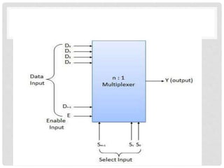
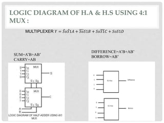
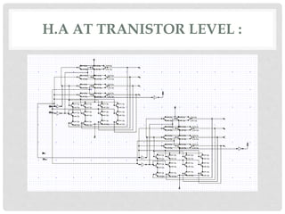
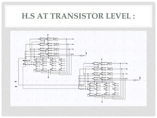
U . S A I R A H U L
HALF- ADDER &
HALF- SUBTRACTOR
USING
4: 1 MULTIPLEXER
COMBINATIONAL CIRCUIT
• Combinational circuit is a circuit in which we combine the different
gates in the circuit for example encoder, decoder, multiplexer and
demultiplexer.
• Combinational circuit consists of logic gates whose outputs depend
on the present inputs.
HALF ADDER
• Half adder is a combinational logic circuit with two inputs and two
outputs. The half adder circuit is designed to add two single bit
binary numbers A and B.
• It is the basic building block for addition of two single bit numbers.
This circuit has two outputs carry and sum.
HALF SUBTRACTOR
• Half subtractor is a combination circuit with two inputs
and two outputs (difference and borrow).
• It produces the difference between the two binary bits at
the input and also produces a output (Borrow) to indicate
if a 1 has been borrowed. In the subtraction (A-B), A is
called as Minuend bit and B is called as Subtrahend bit.
TRUTHTABLE AND LOGIC CIRCUIT :
MULTIPLEXERS
• Multiplexer is a special type of combinational circuit. There are n-data
inputs, one output and m select inputs with 2m = n. It is a digital circuit
which selects one of the n data inputs and routes it to the output. The
selection of one of the n inputs is done by the selected inputs.
• Depending on the digital code applied at the selected inputs, one out of n
data sources is selected and transmitted to the single output Y.
• E is called the strobe or enable input which is useful for the cascading. It is
generally an active low terminal, that means it will perform the required
operation when it is low.
• Multiplexer come in multiple variations:
• 2 : 1 multiplexer
• 4 : 1 multiplexer
• 16 : 1 multiplexer
• 32 : 1 multiplexer
LOGIC DIAGRAM OF H.A & H.S USING 4:1
MUX :
MULTIPLEXER 𝑌 = 𝑆𝑜 𝑆1𝐴 + 𝑆𝑜𝑆1𝐵 + 𝑆𝑜𝑆1𝐶 + 𝑆𝑜𝑆1𝐷
SUM=A’B+AB’
CARRY=AB
DIFFERENCE=A’B+AB’
BORROW=AB’
CMOS LOGIC :
• In this project we use ,CMOS logic .
• CMOS circuits are constructed in such a way that all PMOS transistors must have either
an input from the voltage source or from another PMOS transistor. Similarly,
all NMOS transistors must have either an input from ground or from another NMOS
transistor.
• The composition of a PMOS transistor creates low resistance between its source and
drain contacts when a low gate voltage is applied and high resistance when a high gate
voltage is applied.
• On the other hand, the composition of an NMOS transistor creates high resistance
between source and drain when a low gate voltage is applied and low resistance when a
high gate voltage is applied.
ADVANTAGES & DISADVANTAGES OF
CMOS LOGIC:
• The outputs actively drive both ways i.e bidirectional capability
• Low output drive current
• CMOS logic takes very little power when held in a fixed state i.e low
power dissipation
• High input impedance.
• Can’t drive high capacitive loads
• Some circuits are not practicable
H.A AT TRANISTOR LEVEL :
H.S AT TRANSISTOR LEVEL :
CONCLUSION
• The output of combinational circuit at any instant of time, depends only
on the levels present at input terminals.In this project we are using two
level circuit .
• The combinational circuit do not use any memory. The previous state of
input does not have any effect on the present state of the circuit.
• They have no memory element.Hence there will be no time delay in the
output .
• The schematic of these ciruits are constructed and verified in DSCH
software tool .

halfadder & halfsubtractor using 4:1 MUX

  • 1.
    U . SA I R A H U L HALF- ADDER & HALF- SUBTRACTOR USING 4: 1 MULTIPLEXER
  • 2.
    COMBINATIONAL CIRCUIT • Combinationalcircuit is a circuit in which we combine the different gates in the circuit for example encoder, decoder, multiplexer and demultiplexer. • Combinational circuit consists of logic gates whose outputs depend on the present inputs.
  • 3.
    HALF ADDER • Halfadder is a combinational logic circuit with two inputs and two outputs. The half adder circuit is designed to add two single bit binary numbers A and B. • It is the basic building block for addition of two single bit numbers. This circuit has two outputs carry and sum.
  • 4.
    HALF SUBTRACTOR • Halfsubtractor is a combination circuit with two inputs and two outputs (difference and borrow). • It produces the difference between the two binary bits at the input and also produces a output (Borrow) to indicate if a 1 has been borrowed. In the subtraction (A-B), A is called as Minuend bit and B is called as Subtrahend bit.
  • 5.
  • 6.
    MULTIPLEXERS • Multiplexer isa special type of combinational circuit. There are n-data inputs, one output and m select inputs with 2m = n. It is a digital circuit which selects one of the n data inputs and routes it to the output. The selection of one of the n inputs is done by the selected inputs. • Depending on the digital code applied at the selected inputs, one out of n data sources is selected and transmitted to the single output Y. • E is called the strobe or enable input which is useful for the cascading. It is generally an active low terminal, that means it will perform the required operation when it is low.
  • 8.
    • Multiplexer comein multiple variations: • 2 : 1 multiplexer • 4 : 1 multiplexer • 16 : 1 multiplexer • 32 : 1 multiplexer
  • 9.
    LOGIC DIAGRAM OFH.A & H.S USING 4:1 MUX : MULTIPLEXER 𝑌 = 𝑆𝑜 𝑆1𝐴 + 𝑆𝑜𝑆1𝐵 + 𝑆𝑜𝑆1𝐶 + 𝑆𝑜𝑆1𝐷 SUM=A’B+AB’ CARRY=AB DIFFERENCE=A’B+AB’ BORROW=AB’
  • 10.
    CMOS LOGIC : •In this project we use ,CMOS logic . • CMOS circuits are constructed in such a way that all PMOS transistors must have either an input from the voltage source or from another PMOS transistor. Similarly, all NMOS transistors must have either an input from ground or from another NMOS transistor. • The composition of a PMOS transistor creates low resistance between its source and drain contacts when a low gate voltage is applied and high resistance when a high gate voltage is applied. • On the other hand, the composition of an NMOS transistor creates high resistance between source and drain when a low gate voltage is applied and low resistance when a high gate voltage is applied.
  • 11.
    ADVANTAGES & DISADVANTAGESOF CMOS LOGIC: • The outputs actively drive both ways i.e bidirectional capability • Low output drive current • CMOS logic takes very little power when held in a fixed state i.e low power dissipation • High input impedance. • Can’t drive high capacitive loads • Some circuits are not practicable
  • 12.
  • 13.
  • 14.
    CONCLUSION • The outputof combinational circuit at any instant of time, depends only on the levels present at input terminals.In this project we are using two level circuit . • The combinational circuit do not use any memory. The previous state of input does not have any effect on the present state of the circuit. • They have no memory element.Hence there will be no time delay in the output . • The schematic of these ciruits are constructed and verified in DSCH software tool .