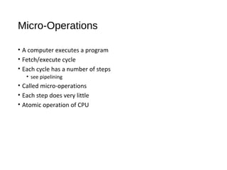
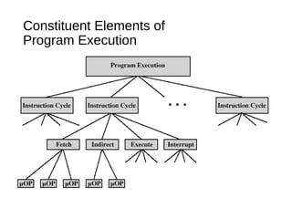
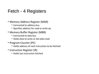
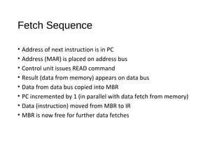
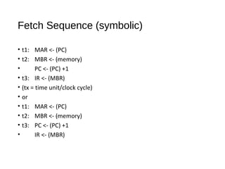
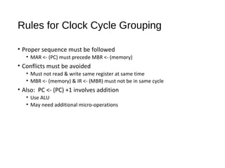
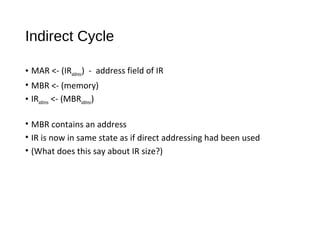
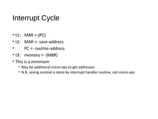
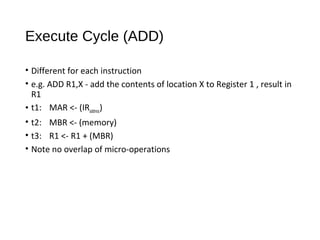
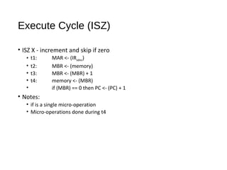
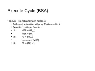
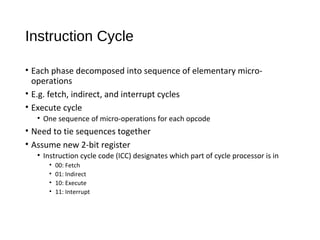
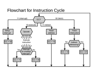
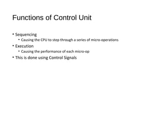
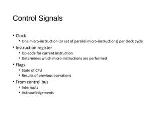
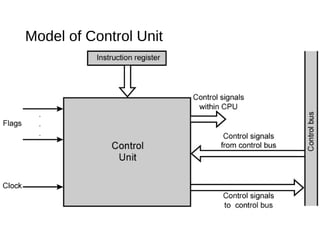
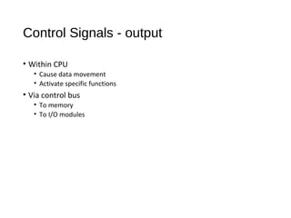
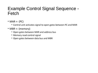
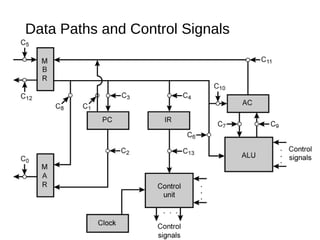
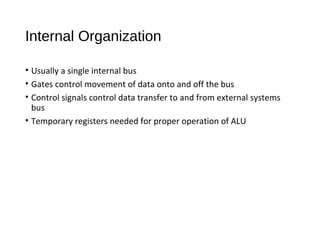
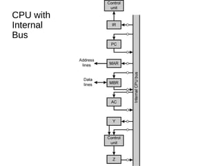
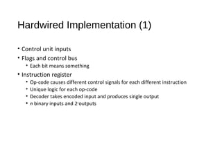
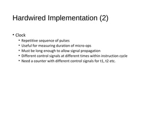
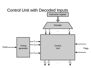
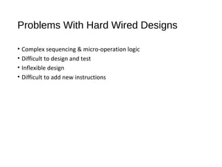
Control Unit Operation
Micro-Operations
• A computer executes a program
• Fetch/execute cycle
• Each cycle has a number of steps
• see pipelining
• Called micro-operations
• Each step does very little
• Atomic operation of CPU
Constituent Elements of
Program Execution
Fetch - 4 Registers
• Memory Address Register (MAR)
• Connected to address bus
• Specifies address for read or write op
• Memory Buffer Register (MBR)
• Connected to data bus
• Holds data to write or last data read
• Program Counter (PC)
• Holds address of next instruction to be fetched
• Instruction Register (IR)
• Holds last instruction fetched
Fetch Sequence
• Address of next instruction is in PC
• Address (MAR) is placed on address bus
• Control unit issues READ command
• Result (data from memory) appears on data bus
• Data from data bus copied into MBR
• PC incremented by 1 (in parallel with data fetch from memory)
• Data (instruction) moved from MBR to IR
• MBR is now free for further data fetches
Fetch Sequence (symbolic)
• t1: MAR <- (PC)
• t2: MBR <- (memory)
• PC <- (PC) +1
• t3: IR <- (MBR)
• (tx = time unit/clock cycle)
• or
• t1: MAR <- (PC)
• t2: MBR <- (memory)
• t3: PC <- (PC) +1
• IR <- (MBR)
Rules for Clock Cycle Grouping
• Proper sequence must be followed
• MAR <- (PC) must precede MBR <- (memory)
• Conflicts must be avoided
• Must not read & write same register at same time
• MBR <- (memory) & IR <- (MBR) must not be in same cycle
• Also: PC <- (PC) +1 involves addition
• Use ALU
• May need additional micro-operations
Indirect Cycle
• MAR <- (IRaddress) - address field of IR
• MBR <- (memory)
• IRaddress <- (MBRaddress)
• MBR contains an address
• IR is now in same state as if direct addressing had been used
• (What does this say about IR size?)
Interrupt Cycle
• t1: MBR <-(PC)
• t2: MAR <- save-address
• PC <- routine-address
• t3: memory <- (MBR)
• This is a minimum
• May be additional micro-ops to get addresses
• N.B. saving context is done by interrupt handler routine, not micro-ops
Execute Cycle (ADD)
• Different for each instruction
• e.g. ADD R1,X - add the contents of location X to Register 1 , result in
R1
• t1: MAR <- (IRaddress)
• t2: MBR <- (memory)
• t3: R1 <- R1 + (MBR)
• Note no overlap of micro-operations
Execute Cycle (ISZ)
• ISZ X - increment and skip if zero
• t1: MAR <- (IRaddress)
• t2: MBR <- (memory)
• t3: MBR <- (MBR) + 1
• t4: memory <- (MBR)
• if (MBR) == 0 then PC <- (PC) + 1
• Notes:
• if is a single micro-operation
• Micro-operations done during t4
Execute Cycle (BSA)
• BSA X - Branch and save address
• Address of instruction following BSA is saved in X
• Execution continues from X+1
• t1: MAR <- (IRaddress)
• MBR <- (PC)
• t2: PC <- (IRaddress)
• memory <- (MBR)
• t3: PC <- (PC) + 1
Instruction Cycle
• Each phase decomposed into sequence of elementary micro-
operations
• E.g. fetch, indirect, and interrupt cycles
• Execute cycle
• One sequence of micro-operations for each opcode
• Need to tie sequences together
• Assume new 2-bit register
• Instruction cycle code (ICC) designates which part of cycle processor is in
• 00: Fetch
• 01: Indirect
• 10: Execute
• 11: Interrupt
Flowchart for Instruction Cycle
Functional Requirements
• Define basic elements of processor
• Describe micro-operations processor performs
• Determine functions control unit must perform
Basic Elements of Processor
• ALU
• Registers
• Internal data pahs
• External data paths
• Control Unit
Types of Micro-operation
• Transfer data between registers
• Transfer data from register to external
• Transfer data from external to register
• Perform arithmetic or logical ops
Functions of Control Unit
• Sequencing
• Causing the CPU to step through a series of micro-operations
• Execution
• Causing the performance of each micro-op
• This is done using Control Signals
Control Signals
• Clock
• One micro-instruction (or set of parallel micro-instructions) per clock cycle
• Instruction register
• Op-code for current instruction
• Determines which micro-instructions are performed
• Flags
• State of CPU
• Results of previous operations
• From control bus
• Interrupts
• Acknowledgements
Model of Control Unit
Control Signals - output
• Within CPU
• Cause data movement
• Activate specific functions
• Via control bus
• To memory
• To I/O modules
Example Control Signal Sequence -
Fetch
• MAR <- (PC)
• Control unit activates signal to open gates between PC and MAR
• MBR <- (memory)
• Open gates between MAR and address bus
• Memory read control signal
• Open gates between data bus and MBR
Data Paths and Control Signals
Internal Organization
• Usually a single internal bus
• Gates control movement of data onto and off the bus
• Control signals control data transfer to and from external systems
bus
• Temporary registers needed for proper operation of ALU
CPU with
Internal
Bus
Intel 8085 CPU Block Diagram
Intel 8085 Pin
Configuration
Intel 8085 OUT Instruction
Timing Diagram
Hardwired Implementation (1)
• Control unit inputs
• Flags and control bus
• Each bit means something
• Instruction register
• Op-code causes different control signals for each different instruction
• Unique logic for each op-code
• Decoder takes encoded input and produces single output
• n binary inputs and 2n
outputs
Hardwired Implementation (2)
• Clock
• Repetitive sequence of pulses
• Useful for measuring duration of micro-ops
• Must be long enough to allow signal propagation
• Different control signals at different times within instruction cycle
• Need a counter with different control signals for t1, t2 etc.
Control Unit with Decoded Inputs
Problems With Hard Wired Designs
• Complex sequencing & micro-operation logic
• Difficult to design and test
• Inflexible design
• Difficult to add new instructions

Control unit

  • 1.
  • 2.
    Micro-Operations • A computerexecutes a program • Fetch/execute cycle • Each cycle has a number of steps • see pipelining • Called micro-operations • Each step does very little • Atomic operation of CPU
  • 3.
  • 4.
    Fetch - 4Registers • Memory Address Register (MAR) • Connected to address bus • Specifies address for read or write op • Memory Buffer Register (MBR) • Connected to data bus • Holds data to write or last data read • Program Counter (PC) • Holds address of next instruction to be fetched • Instruction Register (IR) • Holds last instruction fetched
  • 5.
    Fetch Sequence • Addressof next instruction is in PC • Address (MAR) is placed on address bus • Control unit issues READ command • Result (data from memory) appears on data bus • Data from data bus copied into MBR • PC incremented by 1 (in parallel with data fetch from memory) • Data (instruction) moved from MBR to IR • MBR is now free for further data fetches
  • 6.
    Fetch Sequence (symbolic) •t1: MAR <- (PC) • t2: MBR <- (memory) • PC <- (PC) +1 • t3: IR <- (MBR) • (tx = time unit/clock cycle) • or • t1: MAR <- (PC) • t2: MBR <- (memory) • t3: PC <- (PC) +1 • IR <- (MBR)
  • 7.
    Rules for ClockCycle Grouping • Proper sequence must be followed • MAR <- (PC) must precede MBR <- (memory) • Conflicts must be avoided • Must not read & write same register at same time • MBR <- (memory) & IR <- (MBR) must not be in same cycle • Also: PC <- (PC) +1 involves addition • Use ALU • May need additional micro-operations
  • 8.
    Indirect Cycle • MAR<- (IRaddress) - address field of IR • MBR <- (memory) • IRaddress <- (MBRaddress) • MBR contains an address • IR is now in same state as if direct addressing had been used • (What does this say about IR size?)
  • 9.
    Interrupt Cycle • t1:MBR <-(PC) • t2: MAR <- save-address • PC <- routine-address • t3: memory <- (MBR) • This is a minimum • May be additional micro-ops to get addresses • N.B. saving context is done by interrupt handler routine, not micro-ops
  • 10.
    Execute Cycle (ADD) •Different for each instruction • e.g. ADD R1,X - add the contents of location X to Register 1 , result in R1 • t1: MAR <- (IRaddress) • t2: MBR <- (memory) • t3: R1 <- R1 + (MBR) • Note no overlap of micro-operations
  • 11.
    Execute Cycle (ISZ) •ISZ X - increment and skip if zero • t1: MAR <- (IRaddress) • t2: MBR <- (memory) • t3: MBR <- (MBR) + 1 • t4: memory <- (MBR) • if (MBR) == 0 then PC <- (PC) + 1 • Notes: • if is a single micro-operation • Micro-operations done during t4
  • 12.
    Execute Cycle (BSA) •BSA X - Branch and save address • Address of instruction following BSA is saved in X • Execution continues from X+1 • t1: MAR <- (IRaddress) • MBR <- (PC) • t2: PC <- (IRaddress) • memory <- (MBR) • t3: PC <- (PC) + 1
  • 13.
    Instruction Cycle • Eachphase decomposed into sequence of elementary micro- operations • E.g. fetch, indirect, and interrupt cycles • Execute cycle • One sequence of micro-operations for each opcode • Need to tie sequences together • Assume new 2-bit register • Instruction cycle code (ICC) designates which part of cycle processor is in • 00: Fetch • 01: Indirect • 10: Execute • 11: Interrupt
  • 14.
  • 15.
    Functional Requirements • Definebasic elements of processor • Describe micro-operations processor performs • Determine functions control unit must perform
  • 16.
    Basic Elements ofProcessor • ALU • Registers • Internal data pahs • External data paths • Control Unit
  • 17.
    Types of Micro-operation •Transfer data between registers • Transfer data from register to external • Transfer data from external to register • Perform arithmetic or logical ops
  • 18.
    Functions of ControlUnit • Sequencing • Causing the CPU to step through a series of micro-operations • Execution • Causing the performance of each micro-op • This is done using Control Signals
  • 19.
    Control Signals • Clock •One micro-instruction (or set of parallel micro-instructions) per clock cycle • Instruction register • Op-code for current instruction • Determines which micro-instructions are performed • Flags • State of CPU • Results of previous operations • From control bus • Interrupts • Acknowledgements
  • 20.
  • 21.
    Control Signals -output • Within CPU • Cause data movement • Activate specific functions • Via control bus • To memory • To I/O modules
  • 22.
    Example Control SignalSequence - Fetch • MAR <- (PC) • Control unit activates signal to open gates between PC and MAR • MBR <- (memory) • Open gates between MAR and address bus • Memory read control signal • Open gates between data bus and MBR
  • 23.
    Data Paths andControl Signals
  • 24.
    Internal Organization • Usuallya single internal bus • Gates control movement of data onto and off the bus • Control signals control data transfer to and from external systems bus • Temporary registers needed for proper operation of ALU
  • 25.
  • 26.
    Intel 8085 CPUBlock Diagram
  • 27.
  • 28.
    Intel 8085 OUTInstruction Timing Diagram
  • 29.
    Hardwired Implementation (1) •Control unit inputs • Flags and control bus • Each bit means something • Instruction register • Op-code causes different control signals for each different instruction • Unique logic for each op-code • Decoder takes encoded input and produces single output • n binary inputs and 2n outputs
  • 30.
    Hardwired Implementation (2) •Clock • Repetitive sequence of pulses • Useful for measuring duration of micro-ops • Must be long enough to allow signal propagation • Different control signals at different times within instruction cycle • Need a counter with different control signals for t1, t2 etc.
  • 31.
    Control Unit withDecoded Inputs
  • 32.
    Problems With HardWired Designs • Complex sequencing & micro-operation logic • Difficult to design and test • Inflexible design • Difficult to add new instructions