Download as PDF, PPTX
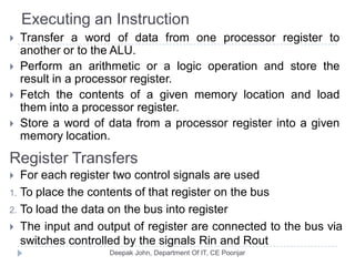
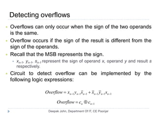
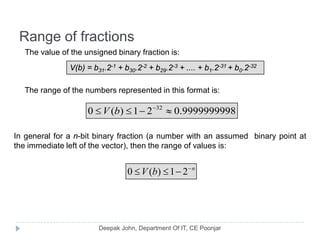
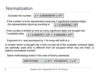
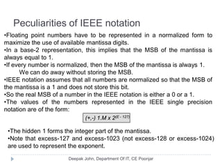
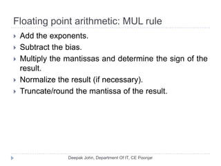
![Executing an Instruction
Fetch the contents of the memory location pointed to by
the PC. The contents of this location are loaded into the
IR (fetch phase).
IR ← [[PC]]
Assuming that the memory is byte addressable,
increment the contents of the PC by 4 (fetch phase).
PC ← [PC] + 4
Carry out the actions specified by the instruction in the
IR (execution phase).](https://image.slidesharecdn.com/compuerorganizaion-processingunit-121107001331-phpapp01/85/Compuer-organizaion-processing-unit-3-320.jpg)


This document discusses the architecture and operation of processing units. It begins by outlining fundamental concepts like how the processor fetches and executes instructions sequentially using the program counter. It then describes the execution of a single instruction through fetch, execution, and incrementing the program counter phases. The document details the components involved in instruction execution like registers, arithmetic logic unit, and memory. It explains the sequencing of control signals to perform operations like register transfers, arithmetic/logic, and memory access. The document compares hardwired and microprogrammed approaches to control and their advantages/disadvantages. It concludes with details on arithmetic operations like addition, subtraction, overflow detection, and fast addition techniques.


![2.4_Design_of_CPU_&_Types_of_Control_Unit[1].pptx](https://cdn.slidesharecdn.com/ss_thumbnails/2-250318152042-1bd3979e-thumbnail.jpg?width=640&height=640&fit=bounds)