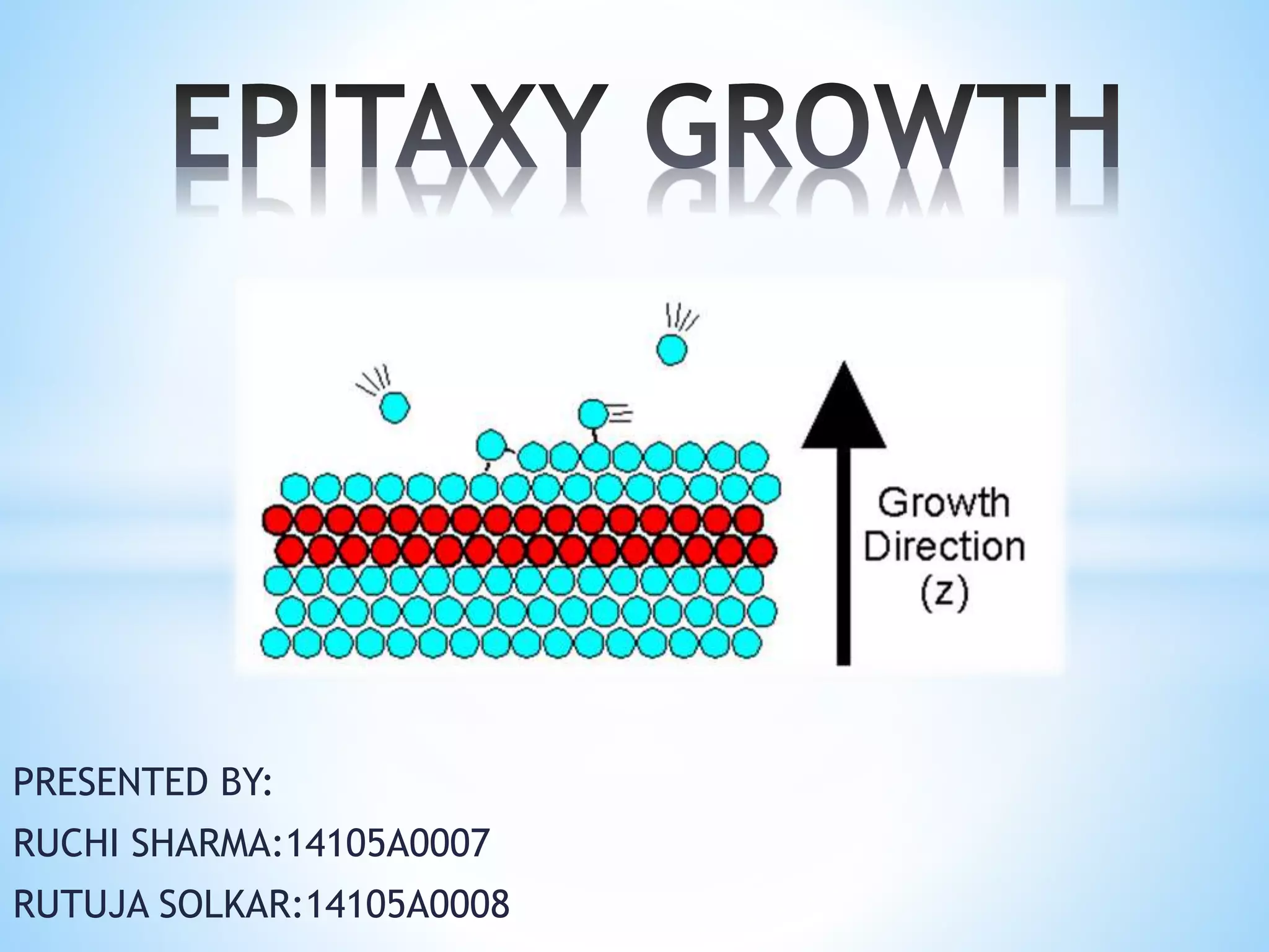
PRESENTED BY:
RUCHI SHARMA:14105A0007
RUTUJA SOLKAR:14105A0008
•Epitaxy refers to the method of depositing a
mono-crystalline film on a mono-crystalline
substrate. The deposited film is denoted as
epitaxial film or epitaxial layer.
•The term epitaxy comes from the Greek roots,
Epi means “above” and taxis means
“deposition in ordered manner”.
•Epitaxial films may be grown from gaseous or
liquid precursors.
•The substrate acts as a seed crystal, the
deposited film takes on a lattice structure
and orientation identical to those of the
substrate.
Types of Epitaxial films
Epitaxial films can be classified into two broad categories:
Homoepitaxy
-The film and the substrate are the same material.
-Epitaxially grown layers are purer than the substrate and can
be doped independently o f it.
Pseudo-homoepitaxy: Epi film and substrate are of same material
but doping in epi layer can be different from that of substrate
(doped Si/undoped Si)
Heteroepitaxy-
Film and substrate are of different materials
Pseudo heteroepitaxy : chemical commonality between film and
substrate
Applications of Epitaxial Growth
• Nanotechnology
• semiconductor fabrication
• high quality crystal growth(silicon –germanium, gallium-nitride)
• to grow layers of pre-doped silicon (in pacemakers, vending
machine)
•To deposit organic molecules onto crystalline substrate.
Liquid Phase Epitaxy
• Liquid phase epitaxy (LPE) is a method to grow semiconductor crystal
layers from the melt on solid substrates
• This happens at temperatures well below the melting point of the
deposited semiconductor
• The semiconductor is dissolved in the melt of another material. At
conditions that are close to the equilibrium between dissolution and
deposition the deposition of the semiconductor crystal on the substrate is
slowly and uniform
• The equilibrium conditions depend very much on the temperature and
on the concentration of the dissolved semiconductor in the melt
ADVANTAGES
• High growth rates. These are typically
0.1–10μm/h, i.e. faster than in VPE or
MBE
• Favorable segregation of impurities into
the liquid phase
• Ability to produce very flat surfaces and
excellent structural perfection
• Wide selection of dopants
• Growth can be made to occur over a
wide range of temperatures
• Absence of highly toxic precursors or
byproducts.
LIMITATIONS
• To control of layer thickness, alloy
compositions,doping,interface
smoothness and difficulties in growing
certain combinations of interest for hetero
structure devices.
• Poor reproducibility, problems with
scaling up in size or throughput
• Atomic layer deposition (ALD) is a thin film deposition technique
that is based on the sequential use of a gas phase chemical process
• ALD is considered a subclass of chemical vapour deposition. The
majority of ALD reactions use two chemicals, typically
called precursors
• These precursors react with the surface of a material one at a time in
a sequential, self-limiting, manner
• Through the repeated exposure to separate precursors, a thin film is
slowly deposited
Advantages
• VPE provides a very controlled method to produce a film to an
atomically specified thickness. Also, the growth of different multilayer
structures is straightforward.
• Due to the sensitivity and precision of the equipment, it is very
beneficial to those in the field of microelectronics and nanotechnology
in producing small, but efficient semiconductors
Disadvantages
• High purity of the substrates is very important, and as such, high costs
will ensue
• Once the layer has been made and the process is complete, there may
be a requirement of needing to remove excess precursors from the
final product
• To make an interesting new crystal using MBE, you start off with a base material
called a substrate, which could be a familiar semiconductor material such as silicon,
germanium, or gallium arsenide
• First, you heat the substrate, typically to some hundreds of degrees (for example,
500–600°C or about 900–1100°F in the case of gallium arsenide)
• Then you fire relatively precise beams of atoms or molecules (heated up so they're
in gas form) at the substrate from "guns" called effusion cells
• The molecules land on the surface of the substrate, condense, and build up very
slowly and systematically in ultra-thin layers, so the complex, single crystal you're
after grows one atomic layer at a time
• That's why MBE is an example of what's called thin-film deposition
Molecular Beam Epitaxy
• Basic elements of MBE
system:
• Heated substrate
• Effusion cells and shutter
• Reflection High Energy
Electron
• Diffraction (RHEED system-
RHEED gun & screen)
• Ultra High Vacuum (UHV)
• Liquid Nitrogen cryopanelling
• The solid source material sublimates
• They provide angular distribution of atoms or molecules in beam
• The substrate is heated to the necessary temperature
• The gaseous elements then condense on the wafer where they may
react with each other to form a layer
• Atoms on clean surface are free to move until
finding correct position in the crystal
lattice to bond
Advantages:
It's particularly good for making high-quality (low-defect, highly uniform)
semiconductor crystals from compounds or from a number of different
elements, instead of from a single element
It also allows extremely thin films to be fabricated in a very precise, carefully
controlled way
Disadvantages:
It's a slow and laborious method (crystal growth rate is typically a few microns
per hour), which means it's more suited for scientific research laboratories than
high-volume production, and the equipment involved is complex and very
expensive (partly because of the difficulty of achieving such clean, high-
vacuum conditions)
Advantages and
Disadvantages of MBE
Epitaxy growth

Epitaxy growth

  • 1.
  • 2.
    •Epitaxy refers tothe method of depositing a mono-crystalline film on a mono-crystalline substrate. The deposited film is denoted as epitaxial film or epitaxial layer. •The term epitaxy comes from the Greek roots, Epi means “above” and taxis means “deposition in ordered manner”. •Epitaxial films may be grown from gaseous or liquid precursors. •The substrate acts as a seed crystal, the deposited film takes on a lattice structure and orientation identical to those of the substrate.
  • 3.
    Types of Epitaxialfilms Epitaxial films can be classified into two broad categories: Homoepitaxy -The film and the substrate are the same material. -Epitaxially grown layers are purer than the substrate and can be doped independently o f it. Pseudo-homoepitaxy: Epi film and substrate are of same material but doping in epi layer can be different from that of substrate (doped Si/undoped Si) Heteroepitaxy- Film and substrate are of different materials Pseudo heteroepitaxy : chemical commonality between film and substrate
  • 4.
    Applications of EpitaxialGrowth • Nanotechnology • semiconductor fabrication • high quality crystal growth(silicon –germanium, gallium-nitride) • to grow layers of pre-doped silicon (in pacemakers, vending machine) •To deposit organic molecules onto crystalline substrate.
  • 5.
    Liquid Phase Epitaxy •Liquid phase epitaxy (LPE) is a method to grow semiconductor crystal layers from the melt on solid substrates • This happens at temperatures well below the melting point of the deposited semiconductor • The semiconductor is dissolved in the melt of another material. At conditions that are close to the equilibrium between dissolution and deposition the deposition of the semiconductor crystal on the substrate is slowly and uniform • The equilibrium conditions depend very much on the temperature and on the concentration of the dissolved semiconductor in the melt
  • 6.
    ADVANTAGES • High growthrates. These are typically 0.1–10μm/h, i.e. faster than in VPE or MBE • Favorable segregation of impurities into the liquid phase • Ability to produce very flat surfaces and excellent structural perfection • Wide selection of dopants • Growth can be made to occur over a wide range of temperatures • Absence of highly toxic precursors or byproducts. LIMITATIONS • To control of layer thickness, alloy compositions,doping,interface smoothness and difficulties in growing certain combinations of interest for hetero structure devices. • Poor reproducibility, problems with scaling up in size or throughput
  • 7.
    • Atomic layerdeposition (ALD) is a thin film deposition technique that is based on the sequential use of a gas phase chemical process • ALD is considered a subclass of chemical vapour deposition. The majority of ALD reactions use two chemicals, typically called precursors • These precursors react with the surface of a material one at a time in a sequential, self-limiting, manner • Through the repeated exposure to separate precursors, a thin film is slowly deposited
  • 8.
    Advantages • VPE providesa very controlled method to produce a film to an atomically specified thickness. Also, the growth of different multilayer structures is straightforward. • Due to the sensitivity and precision of the equipment, it is very beneficial to those in the field of microelectronics and nanotechnology in producing small, but efficient semiconductors Disadvantages • High purity of the substrates is very important, and as such, high costs will ensue • Once the layer has been made and the process is complete, there may be a requirement of needing to remove excess precursors from the final product
  • 9.
    • To makean interesting new crystal using MBE, you start off with a base material called a substrate, which could be a familiar semiconductor material such as silicon, germanium, or gallium arsenide • First, you heat the substrate, typically to some hundreds of degrees (for example, 500–600°C or about 900–1100°F in the case of gallium arsenide) • Then you fire relatively precise beams of atoms or molecules (heated up so they're in gas form) at the substrate from "guns" called effusion cells • The molecules land on the surface of the substrate, condense, and build up very slowly and systematically in ultra-thin layers, so the complex, single crystal you're after grows one atomic layer at a time • That's why MBE is an example of what's called thin-film deposition Molecular Beam Epitaxy
  • 10.
    • Basic elementsof MBE system: • Heated substrate • Effusion cells and shutter • Reflection High Energy Electron • Diffraction (RHEED system- RHEED gun & screen) • Ultra High Vacuum (UHV) • Liquid Nitrogen cryopanelling
  • 11.
    • The solidsource material sublimates • They provide angular distribution of atoms or molecules in beam • The substrate is heated to the necessary temperature • The gaseous elements then condense on the wafer where they may react with each other to form a layer • Atoms on clean surface are free to move until finding correct position in the crystal lattice to bond
  • 12.
    Advantages: It's particularly goodfor making high-quality (low-defect, highly uniform) semiconductor crystals from compounds or from a number of different elements, instead of from a single element It also allows extremely thin films to be fabricated in a very precise, carefully controlled way Disadvantages: It's a slow and laborious method (crystal growth rate is typically a few microns per hour), which means it's more suited for scientific research laboratories than high-volume production, and the equipment involved is complex and very expensive (partly because of the difficulty of achieving such clean, high- vacuum conditions) Advantages and Disadvantages of MBE