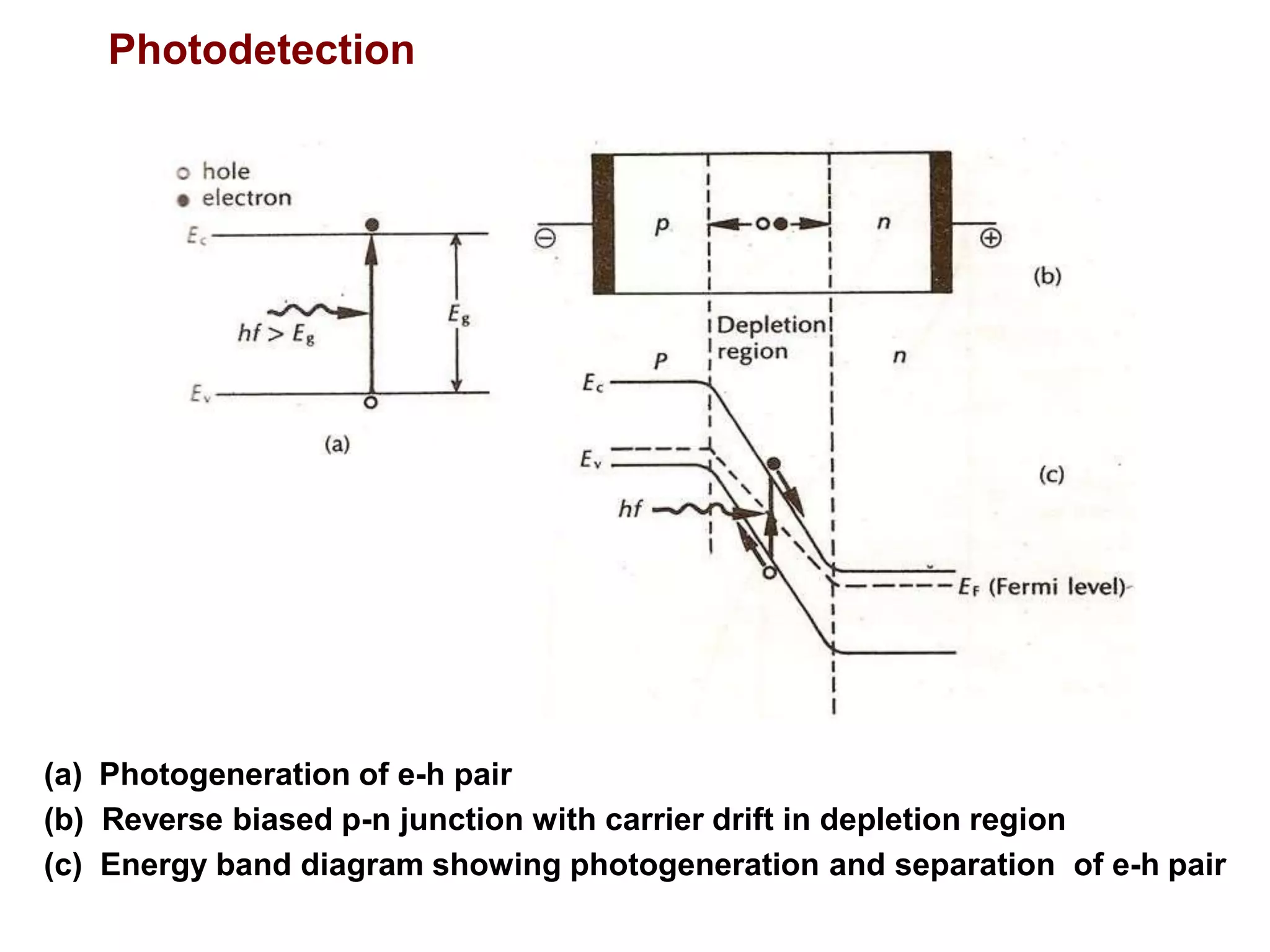
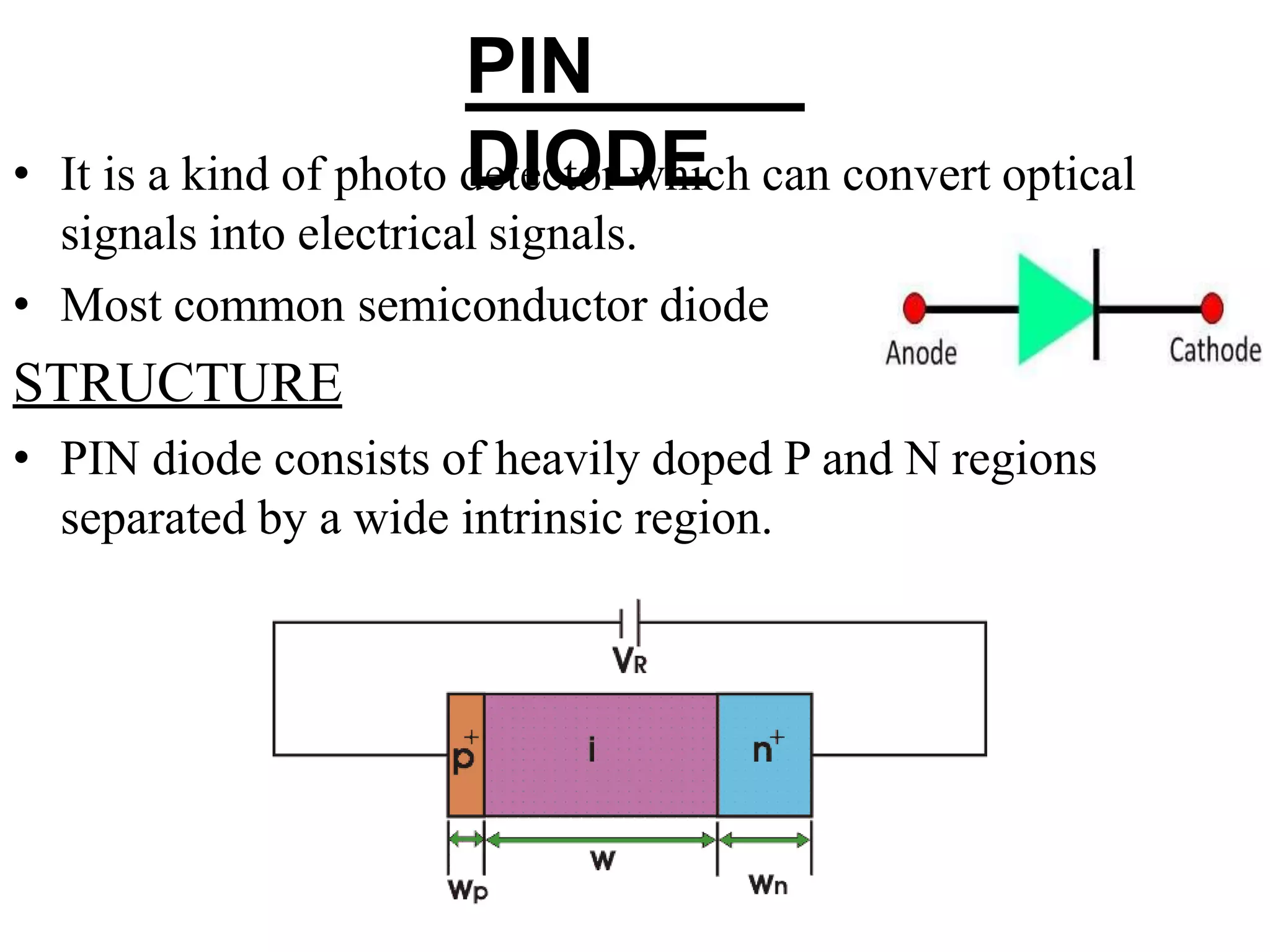
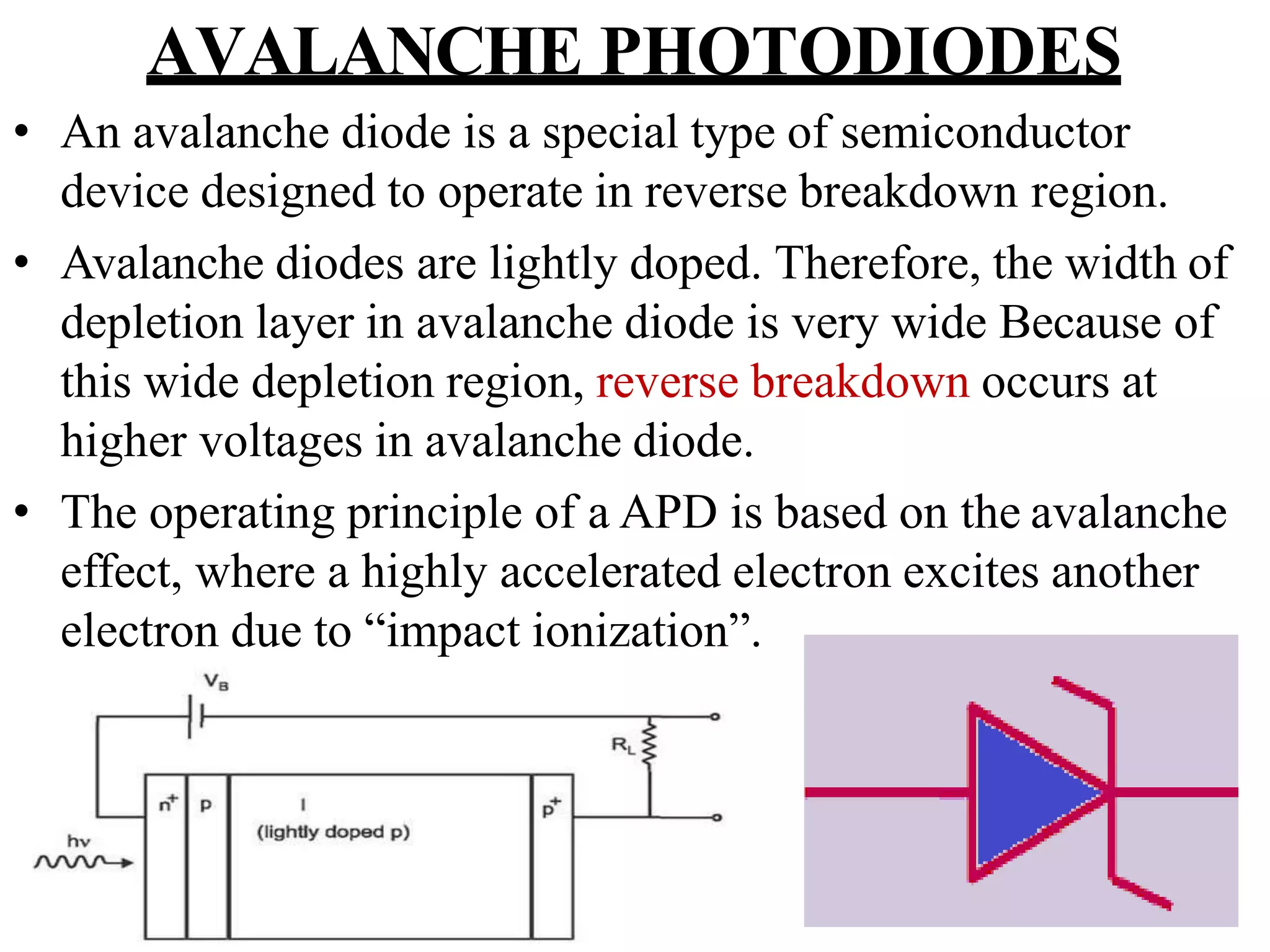
OPTICAL
DETECTORS
• The function of an optical detector is to convert the optical
signal into an electrical signal, which can then be further
processed.
• It senses the luminescent power falling upon it and
converts the variation of this optical power into a
correspondingly varying electric current.
• Characteristics of optical detectors
a. Sensitivity has to be matched to the emission spectra of the
optical transmitter
c. Reliability and Robustness
e. Low Cost
g. Fast response time
b. Linearity
d. Low Noise
f. High quantum efficiency
h. Stability of performance
TYPES OF PHOTO
DETECTORS
1. Photomultipliers,
2. Pyroelectric detectors, and
3. Semiconductor-based photoconductors such as
phototransistors and photodiodes.
• Photomultipliers consists of a photocathode and an
electron multiplier packaged in a vacuum tube. Due to
its large size, it becomes un suitable with optical fiber.
• Pyroelectric detectors involve the conversion of
photons to heat.
• Of the semiconductor-based photo detectors, the
photodiode is used almost exclusively for fiber optic
systems.
• The two types of photodiodes used are the pin
photodetector (PIN)& Avalanche photodiode (APD).
 In semiconductors, conduction band and valence band are
separated by a forbidden band gap.
 Electrons at the valance band are bound. The electrons in the
conduction band are free and when small voltage is applied they
move and causes current flow
 Populating the conduction band with electrons causes the
semiconductor to conduct current.
 The value of band gap Eg determines the conductive properties of
semiconductor
Principle of Photodetection (In Semiconductor)
(a) Photogeneration of e-h pair
(b) Reverse biased p-n junction with carrier drift in depletion region
(c) Energy band diagram showing photogeneration and separation of e-h pair
Photodetection
PIN
DIODE
• It is a kind of photo detector which can convert optical
signals into electrical signals.
• Most common semiconductor diode
STRUCTURE
• PIN diode consists of heavily doped P and N regions
separated by a wide intrinsic region.
• In P-region the hole is the majority charge carrier while in n-
region the electron is the majority charge carrier.
• The intrinsic region has no free charge carrier. It acts as an
insulator between n and the p-type region.
• The i-region has the high resistance which obstructs the flow
of electrons to pass through it.
• PIN diode works as an ordinary PN junction diode frequencies
up to a 100 MHZ. Above 100 MHZ it seizes its operation of
rectifier and behaves as a switch or resistance. In reverse bias
it acts as a capacitor.
Applications
• High voltage rectifier.
• Ideal radio frequency switch.
• Photo detector
• UNBIASED : when the PIN is unbiased there is a diffusion of
electron across the junction. Depletion region is formed
between PI and IN regions
• FORWARD BIAS : When the diode is forward biased, the
injected carrier concentration is typically several orders of
magnitude higher than the intrinsic level carrier concentration.
Due to this high level injection, which in turn is due to the
depletion region , the electric field extends deeply (almost the
entire length) into the region. This electric field helps in
speeding up of the transport of charge carriers from P to N
region, which results in faster operation of the diode, making it
a suitable device for high frequency operations. In forward bias
the diode behaves as a variable resistance and resistance
decreases with increase in forward biasvoltage.
• Reverse Bias : As the reverse bias voltage is increased the
depletion layer thickness increases . The device behaves as a
variable capacitor until the intrinsic region becomes free of mobile
carriers. This voltage is called swept out voltage . At this voltage
the device works asa constant capacitor
.
WORKIN
G
• In normal operation, a sufficiently large reverse bias voltage
is applied across the device so that the intrinsic region is
fully depleted of carriers.
• When an incident photon has energy greater than that or
equal to the band-gap energy of the semiconductor material,
the photon can give up its energy and excite an electron
from the valence band to the conduction band.This process
generates electron-hole pairs.These electrons and holes are
called photocarriers.
• The photodetector is normally designed so that these carriers
are generated mainly in the depleted intrinsic region where
most of the incident light is absorbed.
• The high electric field present in the depletion region causes
the carriers to separate and be collected across the reverse
biased junction.
• This gives to a current flow known as the photocurrent.
• As the charge carriers flow through the material, some
electron-hole pairs will recombine and hence disappear.
• On the average, the charge carriers move a distance Ln or
Lp for electrons and holes, respectively. The distance is
known as diffusion length.
• The time it takes for an electron or hole to recombine is
known as the carrier life time and is represented by τn and
τp respectively.
• The lifetimes and diffusion lengths are related by the
expressions
Ln = (Dn τn)1/2 and Lp = (Dp τp)1/2
Where Dn and Dp are the electron and hole diffusion
constants.
AVALANCHE PHOTODIODES
• An avalanche diode is a special type of semiconductor
device designed to operate in reverse breakdown region.
• Avalanche diodes are lightly doped. Therefore, the width of
depletion layer in avalanche diode is very wide Because of
this wide depletion region, reverse breakdown occurs at
higher voltages in avalanche diode.
• The operating principle of a APD is based on the avalanche
effect, where a highly accelerated electron excites another
electron due to “impact ionization”.
WORKIN
G
• Avalanche diode allows electric current in both forward and
reverse directions.
• When forward bias voltage is applied to the avalanche
diode, it works like a normal p-n junction diode by allowing
electric current through it.
• When reverse bias voltage is applied to the avalanche
diode, the majority carriers are moved away from the
junction and the width of depletion region increases.
• However
, the minority carriers experience arepulsive
force from external voltage and flow from p-type to
n-type and n-type to p-type by carrying the electric
current.This small electric current carried byminority
carriers is called reverse leakagecurrent.
• If the reverse bias voltage applied to the avalanche
diode is further increased, the minority carriers will
gain large amount of energy and accelerated to
greater velocities. These electrons moving at high
speed will collide with the atoms and transfer their
energy to the valenceelectrons.
• The valance electrons which gains enough energy and get
detached from the parent atom and become free electrons.
This carrier multiplication mechanism is known as impact
ionization.
• These free electrons are again accelerated. When these free
electrons again collide with other atoms, they knock off
more electrons.Because of this continuous collision with the
atoms, a large number of minority carriers are generated.
This phenomenon is known as the avalanche effect.
• When the reverse voltage applied to the avalanche diode
continuously increases, at some point the junction
breakdown or avalanche breakdown occurs. At this point, a
small increase in voltage will suddenly increases the electric
current.
• A commonly used structure for achieving carrier
multiplication with very little excess noise is the reach-
through construction.
• The reach-through avalanche photo diode (RAPD) is
composed of a high resistivity p-type material deposited on
a heavily doped p-type substrate.
• P-type diffusion is then made in the high resistivity material
followed by the construction of an n+ layer.
• This configuration is referred to as p+πpn+ reach-through
structure.
• The π layer is basically an intrinsic material, but actually
doped by p-type materials because of imperfect
purification.
• When a low reverse bias voltage is applied, most of
the potential drop is across the pn+ junction.
• The depletion layer widens with increasing bias until a
certain voltage is reached at which the peak electric
field at the pn+ junction is about 5-10 % below that is
needed to cause avalanche breakdown.
• At this point, the depletion layer just ”reaches
through” to the nearly intrinsic π region.
• In the normal usage, RAPD is operated in the fully depleted
p+
mode. Light enters the device through region and is
absorbed in the π material.
• Upon being absorbed, the photon gives up its energy, thereby
creating electron-hole pairs, which are then separated by the
electric filed in the π region.
• The photo generated electrons drift through the π region in the
pn+ junction, where a high electric fieldexists.
• It is in this high-field region that carrier multiplication takes
place.
• The average no: of electron-hole pairs created by a carrier per
unit distance traveled is called the ionization rate.
Applications
• Avalanche diodes can be used as white noise generators.
• Avalanche diodes are used in protecting circuits.
NOISE IN DETECTORS
• Noise is a term generally used to refer to any undesired
disturbances that mask the received signal in a
communication system
• Noise is any electrical or optical energy apart from the
signal itself.
• An optical signal that is too weak cannot be distinguished
from noise.
• The most important noises associated with the photodetector
and the receivers are:
1. Shot Noise
2. Dark Current
3. Thermal Noise
SHOT NOISE
• Discrete nature of electrons causes a signal disturbance
called shot noise.
• Deviation of the actual number of electrons from the
average number is known as shot noise.
• Shot noise arises due to the reason that an electric
current is made up of stream of randomly generated
electrons.
• The shot noise current has a mean-square value in a
receiver bandwidth Be that is proportional to the average
value of photocurrent Ip.
• <i2
shot> = σ2 = 2q I B
shot p e M2 F(M), where F(M) is a
noise figure associated with the nature of the avalanche
process & M is the average of the statistically varying
avalanche gain
THERMAL NOISE
• It is also known as Nyquist noise or Johnson noise
• It arises due to thermal motion of electron in the load
resistor of photodiode circuit.
• This is due to the fact that electrons in any resistor have
random motion.
• Since the electron motion is random, the average value
of this current is zero.
• The mean square thermal noise current in a load resistor
RL is givenby
<i2
TN> = (4KBTB)/RL
Where KB is the Boltzmann’s constant & is 1.38*10-23J/K
TB is the absolutetemperature.
DARK CURRENT NOISE
• When there is no incident optical power even then, a
small reverse leakage current still flows from the
device terminals,called dark current and this
contributes to the total systemnoise.
• It arises from thermally generated carriers.
• It increases with the increase of temperature and
dark current noise is given by
<i 2> = 2q B I ,
d e d
where Id is the dark current.
COMPARIS
ON
WAVELENGTH DIVISION MULTIPLEXING
(WDM)
• WDM is a scheme of combining a number of wavelengths over a
single fiber.
• Each input is generated by a separate optical source with a
unique wavelength.
• An optical multiplexer couples light from individual sources to
the transmitting fiber.
• At the receiving station, an optical demultiplexer is required to
separate the different carriers before detection.
FEATURES /ADVANTAGES
• Capacity can be upgraded
• Scalable ie no of channels can be increased.
• Transparency (Any channel can carry any transmission format)
• Can carry out wavelength switching and wavelength routing.
WDM COMPONENTS
• Wavelength Selective Splitters
• Wavelength Selective Couplers
• Isolators
• Tunable Optical Filter
• Tunable Source
• Optical amplifier
• Add-drop Multiplexer and De-multiplexer
WDM COMPONENTS
Passive devices:
• operate completely in optical domainto split,
isolate and combine lightstreams.
•Couplers, Power splitters, Opticalisolators
Active devices:
• controlled electronically
• Tunable sources, Optical amplifiers, Opticalfilters
OPTICALSPLITTER
• A passive device that splits the optical power carried by a single input
fiber into two output fibers.
• The input optical power is normally split evenly between the two output
fibers. This type of optical splitter is known as aY-coupler.
• An optical splitter may distribute the optical power carried by input
power in an uneven manner. This type of optical splitter is known as a T-
coupler, or an optical tap.
OPTICALCOMBINER
• A passive device that combines the optical power carried by two input
fibers into a single output fiber.
• An X coupler combines the functions of the optical splitter and combiner.
STAR COUPLER
• Multiport couplers that distributes optical power from more than two
input ports among several output ports.
TREE COUPLER
• Multiport couplers that splits the optical power from one input fiber to
more than two output fibers.
DIRECTIONALCOUPLER
• Directional couplers are fiber optic couplers that prevent the transfer
of optical power from one input fiber to another input fiber.
SYMMETRICALCOUPLER
• transmits the same amount of power through the coupler when the
input and output fibers are reversed.

Optical Detectors.pptx

  • 1.
    OPTICAL DETECTORS • The functionof an optical detector is to convert the optical signal into an electrical signal, which can then be further processed. • It senses the luminescent power falling upon it and converts the variation of this optical power into a correspondingly varying electric current. • Characteristics of optical detectors a. Sensitivity has to be matched to the emission spectra of the optical transmitter c. Reliability and Robustness e. Low Cost g. Fast response time b. Linearity d. Low Noise f. High quantum efficiency h. Stability of performance
  • 2.
    TYPES OF PHOTO DETECTORS 1.Photomultipliers, 2. Pyroelectric detectors, and 3. Semiconductor-based photoconductors such as phototransistors and photodiodes. • Photomultipliers consists of a photocathode and an electron multiplier packaged in a vacuum tube. Due to its large size, it becomes un suitable with optical fiber. • Pyroelectric detectors involve the conversion of photons to heat. • Of the semiconductor-based photo detectors, the photodiode is used almost exclusively for fiber optic systems. • The two types of photodiodes used are the pin photodetector (PIN)& Avalanche photodiode (APD).
  • 3.
     In semiconductors,conduction band and valence band are separated by a forbidden band gap.  Electrons at the valance band are bound. The electrons in the conduction band are free and when small voltage is applied they move and causes current flow  Populating the conduction band with electrons causes the semiconductor to conduct current.  The value of band gap Eg determines the conductive properties of semiconductor Principle of Photodetection (In Semiconductor)
  • 4.
    (a) Photogeneration ofe-h pair (b) Reverse biased p-n junction with carrier drift in depletion region (c) Energy band diagram showing photogeneration and separation of e-h pair Photodetection
  • 5.
    PIN DIODE • It isa kind of photo detector which can convert optical signals into electrical signals. • Most common semiconductor diode STRUCTURE • PIN diode consists of heavily doped P and N regions separated by a wide intrinsic region.
  • 6.
    • In P-regionthe hole is the majority charge carrier while in n- region the electron is the majority charge carrier. • The intrinsic region has no free charge carrier. It acts as an insulator between n and the p-type region. • The i-region has the high resistance which obstructs the flow of electrons to pass through it. • PIN diode works as an ordinary PN junction diode frequencies up to a 100 MHZ. Above 100 MHZ it seizes its operation of rectifier and behaves as a switch or resistance. In reverse bias it acts as a capacitor. Applications • High voltage rectifier. • Ideal radio frequency switch. • Photo detector
  • 7.
    • UNBIASED :when the PIN is unbiased there is a diffusion of electron across the junction. Depletion region is formed between PI and IN regions • FORWARD BIAS : When the diode is forward biased, the injected carrier concentration is typically several orders of magnitude higher than the intrinsic level carrier concentration. Due to this high level injection, which in turn is due to the depletion region , the electric field extends deeply (almost the entire length) into the region. This electric field helps in speeding up of the transport of charge carriers from P to N region, which results in faster operation of the diode, making it a suitable device for high frequency operations. In forward bias the diode behaves as a variable resistance and resistance decreases with increase in forward biasvoltage. • Reverse Bias : As the reverse bias voltage is increased the depletion layer thickness increases . The device behaves as a variable capacitor until the intrinsic region becomes free of mobile carriers. This voltage is called swept out voltage . At this voltage the device works asa constant capacitor .
  • 8.
    WORKIN G • In normaloperation, a sufficiently large reverse bias voltage is applied across the device so that the intrinsic region is fully depleted of carriers. • When an incident photon has energy greater than that or equal to the band-gap energy of the semiconductor material, the photon can give up its energy and excite an electron from the valence band to the conduction band.This process generates electron-hole pairs.These electrons and holes are called photocarriers.
  • 9.
    • The photodetectoris normally designed so that these carriers are generated mainly in the depleted intrinsic region where most of the incident light is absorbed. • The high electric field present in the depletion region causes the carriers to separate and be collected across the reverse biased junction. • This gives to a current flow known as the photocurrent. • As the charge carriers flow through the material, some electron-hole pairs will recombine and hence disappear.
  • 10.
    • On theaverage, the charge carriers move a distance Ln or Lp for electrons and holes, respectively. The distance is known as diffusion length. • The time it takes for an electron or hole to recombine is known as the carrier life time and is represented by τn and τp respectively. • The lifetimes and diffusion lengths are related by the expressions Ln = (Dn τn)1/2 and Lp = (Dp τp)1/2 Where Dn and Dp are the electron and hole diffusion constants.
  • 11.
    AVALANCHE PHOTODIODES • Anavalanche diode is a special type of semiconductor device designed to operate in reverse breakdown region. • Avalanche diodes are lightly doped. Therefore, the width of depletion layer in avalanche diode is very wide Because of this wide depletion region, reverse breakdown occurs at higher voltages in avalanche diode. • The operating principle of a APD is based on the avalanche effect, where a highly accelerated electron excites another electron due to “impact ionization”.
  • 12.
    WORKIN G • Avalanche diodeallows electric current in both forward and reverse directions. • When forward bias voltage is applied to the avalanche diode, it works like a normal p-n junction diode by allowing electric current through it.
  • 13.
    • When reversebias voltage is applied to the avalanche diode, the majority carriers are moved away from the junction and the width of depletion region increases. • However , the minority carriers experience arepulsive force from external voltage and flow from p-type to n-type and n-type to p-type by carrying the electric current.This small electric current carried byminority carriers is called reverse leakagecurrent. • If the reverse bias voltage applied to the avalanche diode is further increased, the minority carriers will gain large amount of energy and accelerated to greater velocities. These electrons moving at high speed will collide with the atoms and transfer their energy to the valenceelectrons.
  • 14.
    • The valanceelectrons which gains enough energy and get detached from the parent atom and become free electrons. This carrier multiplication mechanism is known as impact ionization. • These free electrons are again accelerated. When these free electrons again collide with other atoms, they knock off more electrons.Because of this continuous collision with the atoms, a large number of minority carriers are generated. This phenomenon is known as the avalanche effect. • When the reverse voltage applied to the avalanche diode continuously increases, at some point the junction breakdown or avalanche breakdown occurs. At this point, a small increase in voltage will suddenly increases the electric current.
  • 15.
    • A commonlyused structure for achieving carrier multiplication with very little excess noise is the reach- through construction. • The reach-through avalanche photo diode (RAPD) is composed of a high resistivity p-type material deposited on a heavily doped p-type substrate. • P-type diffusion is then made in the high resistivity material followed by the construction of an n+ layer. • This configuration is referred to as p+πpn+ reach-through structure. • The π layer is basically an intrinsic material, but actually doped by p-type materials because of imperfect purification.
  • 16.
    • When alow reverse bias voltage is applied, most of the potential drop is across the pn+ junction. • The depletion layer widens with increasing bias until a certain voltage is reached at which the peak electric field at the pn+ junction is about 5-10 % below that is needed to cause avalanche breakdown. • At this point, the depletion layer just ”reaches through” to the nearly intrinsic π region.
  • 17.
    • In thenormal usage, RAPD is operated in the fully depleted p+ mode. Light enters the device through region and is absorbed in the π material. • Upon being absorbed, the photon gives up its energy, thereby creating electron-hole pairs, which are then separated by the electric filed in the π region. • The photo generated electrons drift through the π region in the pn+ junction, where a high electric fieldexists. • It is in this high-field region that carrier multiplication takes place. • The average no: of electron-hole pairs created by a carrier per unit distance traveled is called the ionization rate. Applications • Avalanche diodes can be used as white noise generators. • Avalanche diodes are used in protecting circuits.
  • 18.
    NOISE IN DETECTORS •Noise is a term generally used to refer to any undesired disturbances that mask the received signal in a communication system • Noise is any electrical or optical energy apart from the signal itself. • An optical signal that is too weak cannot be distinguished from noise. • The most important noises associated with the photodetector and the receivers are: 1. Shot Noise 2. Dark Current 3. Thermal Noise
  • 19.
    SHOT NOISE • Discretenature of electrons causes a signal disturbance called shot noise. • Deviation of the actual number of electrons from the average number is known as shot noise. • Shot noise arises due to the reason that an electric current is made up of stream of randomly generated electrons. • The shot noise current has a mean-square value in a receiver bandwidth Be that is proportional to the average value of photocurrent Ip. • <i2 shot> = σ2 = 2q I B shot p e M2 F(M), where F(M) is a noise figure associated with the nature of the avalanche process & M is the average of the statistically varying avalanche gain
  • 20.
    THERMAL NOISE • Itis also known as Nyquist noise or Johnson noise • It arises due to thermal motion of electron in the load resistor of photodiode circuit. • This is due to the fact that electrons in any resistor have random motion. • Since the electron motion is random, the average value of this current is zero. • The mean square thermal noise current in a load resistor RL is givenby <i2 TN> = (4KBTB)/RL Where KB is the Boltzmann’s constant & is 1.38*10-23J/K TB is the absolutetemperature.
  • 21.
    DARK CURRENT NOISE •When there is no incident optical power even then, a small reverse leakage current still flows from the device terminals,called dark current and this contributes to the total systemnoise. • It arises from thermally generated carriers. • It increases with the increase of temperature and dark current noise is given by <i 2> = 2q B I , d e d where Id is the dark current.
  • 22.
  • 23.
    WAVELENGTH DIVISION MULTIPLEXING (WDM) •WDM is a scheme of combining a number of wavelengths over a single fiber. • Each input is generated by a separate optical source with a unique wavelength. • An optical multiplexer couples light from individual sources to the transmitting fiber. • At the receiving station, an optical demultiplexer is required to separate the different carriers before detection.
  • 24.
    FEATURES /ADVANTAGES • Capacitycan be upgraded • Scalable ie no of channels can be increased. • Transparency (Any channel can carry any transmission format) • Can carry out wavelength switching and wavelength routing. WDM COMPONENTS • Wavelength Selective Splitters • Wavelength Selective Couplers • Isolators • Tunable Optical Filter • Tunable Source • Optical amplifier • Add-drop Multiplexer and De-multiplexer
  • 25.
    WDM COMPONENTS Passive devices: •operate completely in optical domainto split, isolate and combine lightstreams. •Couplers, Power splitters, Opticalisolators Active devices: • controlled electronically • Tunable sources, Optical amplifiers, Opticalfilters
  • 26.
    OPTICALSPLITTER • A passivedevice that splits the optical power carried by a single input fiber into two output fibers. • The input optical power is normally split evenly between the two output fibers. This type of optical splitter is known as aY-coupler. • An optical splitter may distribute the optical power carried by input power in an uneven manner. This type of optical splitter is known as a T- coupler, or an optical tap. OPTICALCOMBINER • A passive device that combines the optical power carried by two input fibers into a single output fiber. • An X coupler combines the functions of the optical splitter and combiner.
  • 27.
    STAR COUPLER • Multiportcouplers that distributes optical power from more than two input ports among several output ports. TREE COUPLER • Multiport couplers that splits the optical power from one input fiber to more than two output fibers. DIRECTIONALCOUPLER • Directional couplers are fiber optic couplers that prevent the transfer of optical power from one input fiber to another input fiber. SYMMETRICALCOUPLER • transmits the same amount of power through the coupler when the input and output fibers are reversed.