TRANSISTOR_ CONSTRUCTION & WORKING IN HINDI|BIPOLAR JUNCTION TRANSISTOR|NPN_PNP TYPE TRANSISTOR
•
3 likes•561 views

#TRANSISTOR #WORKINGOFTRANSISTROR #PNP_NPN_TRANSISTOR #TRANSISTOR_AS_AMPLIFIER #BJT_UJT_FET_MOSFET_TRANSISTOR #TRANSISTOR_BIASING #TRANSISTOR_IN_HINDI #APPLICAION_OF_TRANSISTOR #VICHARACTERISTICSOFPNJUNCTIONDIODEINHINDIहिंदी #DIODECHARECTERISTICS #PN_DIODE_IN_HINDI #FORWARD_REVERSE_BIASED_DIODE #PN_JUNCTION_DIODE #PNJUNCTIONDIODEUNACADEMY #SEMINCONDUCTORDIODEINHINDI #BASICELECTRICALELECTRONICSENGINEERING #BEEE #RGPV #SAIACADEMYOFELECTRICALENGINEERING #SAEE #ELECTRONICSEMICONDUCTORDEVICE #EDC #ADC #GATE #IES #SSCJE #RRB #NTPC #BHEL #interviewelectricalengineering

Recommended
More Related Content
What's hot
What's hot (20)
Similar to TRANSISTOR_ CONSTRUCTION & WORKING IN HINDI|BIPOLAR JUNCTION TRANSISTOR|NPN_PNP TYPE TRANSISTOR
Similar to TRANSISTOR_ CONSTRUCTION & WORKING IN HINDI|BIPOLAR JUNCTION TRANSISTOR|NPN_PNP TYPE TRANSISTOR (20)
More from Prasant Kumar
More from Prasant Kumar (20)
Recently uploaded
Recently uploaded (20)
TRANSISTOR_ CONSTRUCTION & WORKING IN HINDI|BIPOLAR JUNCTION TRANSISTOR|NPN_PNP TYPE TRANSISTOR
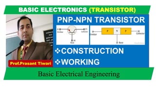
- 1. Basic Electrical Engineering PNP-NPN TRANSISTOR CONSTRUCTION WORKINGProf.Prasant Tiwari
- 2. The word Transistor stands for Transfer of Resistor . It is current controlled device. It has many types, of which BJT is one. BJT is broadly classified into 2 types NPN and PNP . The main function of BJT Transistor is amplification. The small amount of base current controlled both the emitter and collector current. The transistor has two crystal diodes connected back to back. The left side of the diode in known as the emitter-base diode and the right side of the diode is known as the collector-base diode. TRANSISTOR DEFINITION
- 3. The transistor in which one n-type material is doped with two p-type materials such type of transistor is known as PNP transistor. It is a current controlled device. The small amount of base current controlled both the emitter and collector current. The hole is the majority carriers of the PNP transistors which constitute the current in it. The current inside the transistor is constituted because of the changing position of holes and in the leads of the transistor. It is because of the flow of the electrons. The PNP transistor turns on when a small current flows through the base. The direction of current in PNP transistor is from the emitter to collector. PNP TRANSISTOR P N P CONSTRUCTION
- 4. WORKING OF PNP TRANSISTOR The emitter-base junction is connected in forward biased due to which the emitter pushes the holes in the base region. These holes constitute the emitter current. When these holes move into the N-type semiconductor material or base, they combined with the electrons. The base of the transistor is thin and very lightly doped. Hence only a few holes combined with the electrons and the remaining are moved towards the collector space charge layer. Hence develops the base current.
- 5. NPN TRANSISTOR The transistor in which one p-type material is placed between two n-type materials is known as NPN transistor. The NPN transistor amplifies the weak signal enter into the base and produces strong amplify signals at the collector end. In NPN transistor, the direction of movement of an electron is from the emitter to collector region due to which the current constitutes in the transistor. Such type of transistor is mostly used in the circuit because their majority charge carriers are electrons which have high mobility as compared to holes. The NPN transistor has two diodes connected back to back. The diode on the left side is called an emitter-base diode, and the diodes on the right side are called collector-base diode.
- 6. WORKING OFNPN TRANSISTOR The forward biased is applied across the emitter-base junction, and the reversed biased is applied across the collector-base junction. The forward biased voltage VEB is small as compared to the reverse bias voltage VCB. The emitter of the NPN transistor is heavily doped. When the forward bias is applied across the emitter, the majority charge carriers move towards the base. This causes the emitter current IE. The electrons enter into the P-type material and combine with the holes. The base of the NPN transistor is lightly doped. Due to which only a few electrons are combined and remaining constitutes the base current IB.
- 7. PLZ VISIT YPUTUBE CHANNEL FOR VIDEO LINK IS GIVEN IN DESCRIPTION BOX