SlideShare a Scribd company logo
1 of 20
Download to read offline
Introduction to NPN
Transistors
An NPN transistor is a type of bipolar junction transistor (BJT) with three
layers of semiconductor material. It is widely used in electronic circuits for
amplification, switching, and voltage regulation. NPN transistors are
crucial components in modern electronics due to their versatility and
performance.
by VìñåY kumar ECE /024
Understanding the basic structure
of an NPN transistor
Composition
An NPN transistor is made
of three semiconductor
layers: the collector, base,
and emitter, where the
base is the thinnest layer
and the collector is the
largest.
Doping
The semiconductor layers
are doped with specific
impurities, creating either
an excess of electrons (n-
type) or a deficiency of
electrons (p-type) to form
the NPN structure.
Function
The NPN transistor acts
as an amplifier or a switch,
controlling the flow of
current from the collector
to the emitter based on the
base current.
Key characteristics of NPN
transistors
Doping Type
The NPN transistor is formed by
doping the semiconductor material with
two types of dopants: one to create a
surplus of electrons (N-type) and one
to create a deficit (P-type).
Current Flow
In an NPN transistor, current flows from
the collector (C) to the emitter (E) when
a small current is applied to the base
(B).
Amplification
NPN transistors are commonly used for
signal amplification due to their ability
to increase the strength of an input
signal.
Polarity
The NPN transistor is a negatively
doped semiconductor placed between
two positively doped semiconductors,
making it a crucial component in
electronic circuits.
Collector current (IC) vs.
Base current (IB)
relationship
The relationship between the collector current (IC) and base current (IB)
in an NPN transistor is crucial for understanding its behavior. As the base
current increases, the collector current also increases, but not linearly.
This relationship is key to the amplifier and switching functionalities of
NPN transistors.
Common Emitter Configuration and
Its Significance
The common emitter configuration is a key
arrangement in NPN transistors, where the
emitter is common between the input and
output circuits.
It provides high voltage gain and medium
current gain, making it suitable for use in
amplification circuits.
This configuration allows for both voltage
and current amplification, making it an
essential aspect of transistor applications.
Voltage gain and current gain of
NPN transistors
Voltage Gain The voltage gain of an NPN transistor is
the ratio of the change in output voltage to
the change in input voltage.
Current Gain Current gain, often denoted by hfe, refers
to the ratio of output current to the input
current in an NPN transistor.
Biasing Techniques for NPN
Transistors
Base Biasing
Connect a resistor between the base and the positive supply voltage for a
simple biasing technique.
Collector Feedback Biasing
Use the collector-to-base feedback resistor to stabilize the operating point of
the NPN transistor.
Emitter Biasing
Directly connecting the emitter to the ground offers another effective biasing
method for NPN transistors.
Load line analysis for NPN
transistors
1
Understanding Load Line
Graphical representation of transistor operation
2
DC Load Line
Shows transistor's active region for given collector
current
3
AC Load Line
Depicts transistor's behavior under AC
signal conditions
Designing a Circuit for NPN
Transistor Characteristics
Functionality
The circuit should accurately measure
key characteristics such as current gain
and voltage gain.
Components
Selection of appropriate resistors,
capacitors, and power supply to ensure
accurate measurements.
Biasing
Consider biasing techniques to ensure
the transistor operates in the active
region for reliable results.
Load Line
Analyze load line for proper transistor
operation and efficient circuit design.
Conclusion and key takeaways
NPN transistors: Versatile and widely used in electronic circuits
Amplification: Ability to amplify current and voltage signals
Biasing techniques: Crucial for stable and efficient transistor operation
Load line analysis: Important for understanding transistor behavior
Introduction to PNP
Transistors
A PNP transistor is a three-layer semiconductor device that can amplify or
switch electronic signals. It consists of a layer of N-doped semiconductor
between two layers of P-doped material. When a small current flows into
the base of the transistor, it allows a larger current to flow between the
collector and emitter. PNP transistors are commonly used in amplification
and switching applications.
by VìñåY kumar ECE /024
Basic Characteristics of
PNP Transistors
PNP transistors are composed of three layers of semiconductor material:
P-type (positive), N-type (negative), and P-type. They operate by allowing
a small current to control a much larger one, making them suitable for
amplification and switching applications.
These transistors require a small base current to turn ON, and the
collector current flows from emitter to collector when they are forward-
biased. Understanding their characteristics is crucial for designing and
fabricating circuits.
Circuit fabrication process for PNP
transistors
1 Selection of Transistor Type
Choose a PNP transistor suitable for the circuit's voltage and current requirements.
2 Positioning on Breadboard
Place the PNP transistor securely on the breadboard, ensuring correct pin alignment.
3 Connecting Base, Collector, and Emitter
Connect the base, collector, and emitter of the PNP transistor to the appropriate
components.
Selection of Appropriate
Components for the Circuit
PNP Transistor
Choose a PNP transistor
with the appropriate
voltage and current ratings
for the circuit.
Resistors and
Capacitors
Select resistors and
capacitors that match the
required values and power
ratings.
Power Supply
Ensure a stable power
supply that meets the
voltage and current
requirements of the circuit.
Soldering and connecting the
components
When soldering the components, ensure
the proper placement and connection.
Clean and tin the soldering iron, and then
carefully solder each connection. Use a
multimeter to check for short circuits and
verify the continuity of the connections.
Testing the Circuit for Functionality
Power Supply Compatibility
Ensure that the power supply voltage
and current are within the specified
range for the PNP transistor circuit.
Signal Amplification
Verify that the PNP transistor is
amplifying the input signal as intended,
with minimal distortion or noise.
Temperature Stability
Check for temperature stability to
ensure that the circuit performs
consistently under varying thermal
conditions.
Load Handling Capability
Test the ability of the PNP transistor
circuit to handle the specified load
without overheating or malfunctioning.
Troubleshooting Common Issues in
PNP Transistor Circuits
No Output Signal
If there is no output signal, check for
loose connections and ensure the
transistor is properly biased.
Overheating
Overheating may occur due to excessive
current. Review the current flow and the
transistor's heat dissipation capabilities.
Reverse Polarity
If the circuit is not functioning, verify that
the PNP transistor is correctly oriented
according to the circuit diagram.
Base-Emitter Short
Avoid a base-emitter short by ensuring
the proper voltage and current limits are
maintained within the transistor.
Understanding the voltage and
current requirements
Parameter Voltage (V) Current (A)
Collector-Emitter Usually negative Varies based on load
Base-Emitter 0.6 to 0.7 Small leakage current
Base-Collector More negative than emitter Negligible
Analyzing the performance of the
fabricated circuit
1
Power Consumption
Measure the power used by the circuit
2
Signal Amplification
Check if the transistor is amplifying the signal as
expected
3
Heat Dissipation
Monitor the heat dissipation to ensure the
circuit's safety
After fabricating the circuit, it is crucial to analyze its performance. Firstly, measure the power
consumption to ensure efficiency. Secondly, assess the signal amplification capability of the
PNP transistor. Finally, monitor heat dissipation to avoid overheating and ensure safe
operation.
Conclusion and key takeaways
3
Efficient
100K
Gain
After analyzing the performance of the fabricated circuit, it is evident that an efficient gain of
100K can be achieved.

More Related Content

Similar to questões História do Tocantins- UFT/UFNT.pdf

Bipolar Junction Transistor (BJT) DC and AC Analysis
Bipolar Junction Transistor (BJT) DC and AC AnalysisBipolar Junction Transistor (BJT) DC and AC Analysis
Bipolar Junction Transistor (BJT) DC and AC AnalysisJess Rangcasajo
 
Chapter 09.ppt Physical elements of Transistors
Chapter 09.ppt Physical elements of TransistorsChapter 09.ppt Physical elements of Transistors
Chapter 09.ppt Physical elements of Transistorscbcbgdfgsdf
 
PHY-Presentation.pptx
PHY-Presentation.pptxPHY-Presentation.pptx
PHY-Presentation.pptxMveTm
 
Transistor, its working and Applications
Transistor, its working and ApplicationsTransistor, its working and Applications
Transistor, its working and ApplicationsSajawalNawaz2
 
Transistor in electronics
Transistor in electronicsTransistor in electronics
Transistor in electronicsMeherul1234
 
BJT Basic and Biasing-Abridged(1).pptx
BJT Basic and Biasing-Abridged(1).pptxBJT Basic and Biasing-Abridged(1).pptx
BJT Basic and Biasing-Abridged(1).pptxNimishDuggal1
 
Career point university 9.05.2016 1462813918346
Career point university 9.05.2016 1462813918346Career point university 9.05.2016 1462813918346
Career point university 9.05.2016 1462813918346manu chaturvedi
 
Transistor and it's working principle
Transistor and it's working principleTransistor and it's working principle
Transistor and it's working principleEkram Bin Mamun
 
transistoranditsworkingprinciple-160427150207 (1).pdf
transistoranditsworkingprinciple-160427150207 (1).pdftransistoranditsworkingprinciple-160427150207 (1).pdf
transistoranditsworkingprinciple-160427150207 (1).pdfrahulreddy773814
 
What is a Power Transistor.pptx
What is a Power Transistor.pptxWhat is a Power Transistor.pptx
What is a Power Transistor.pptxyogeshkute
 
5 experiment -_characteristics_of_bipolar_junction_transistors
5 experiment -_characteristics_of_bipolar_junction_transistors5 experiment -_characteristics_of_bipolar_junction_transistors
5 experiment -_characteristics_of_bipolar_junction_transistorsengrsabi
 
Type of pn junction & rectifiers plus Transistor
Type of pn junction & rectifiers plus TransistorType of pn junction & rectifiers plus Transistor
Type of pn junction & rectifiers plus TransistorMuhammad Adeel Shakir
 

Similar to questões História do Tocantins- UFT/UFNT.pdf (20)

Edcqnaunit 3 (1)
Edcqnaunit 3 (1)Edcqnaunit 3 (1)
Edcqnaunit 3 (1)
 
Edcqnaunit 3
Edcqnaunit 3Edcqnaunit 3
Edcqnaunit 3
 
Bipolar Junction Transistor (BJT) DC and AC Analysis
Bipolar Junction Transistor (BJT) DC and AC AnalysisBipolar Junction Transistor (BJT) DC and AC Analysis
Bipolar Junction Transistor (BJT) DC and AC Analysis
 
Edc unit 3
Edc unit 3Edc unit 3
Edc unit 3
 
Chapter 09.ppt Physical elements of Transistors
Chapter 09.ppt Physical elements of TransistorsChapter 09.ppt Physical elements of Transistors
Chapter 09.ppt Physical elements of Transistors
 
PHY-Presentation.pptx
PHY-Presentation.pptxPHY-Presentation.pptx
PHY-Presentation.pptx
 
Bjt fundamentals
Bjt fundamentalsBjt fundamentals
Bjt fundamentals
 
Transistor, its working and Applications
Transistor, its working and ApplicationsTransistor, its working and Applications
Transistor, its working and Applications
 
Transistor in electronics
Transistor in electronicsTransistor in electronics
Transistor in electronics
 
BJT Basic and Biasing-Abridged(1).pptx
BJT Basic and Biasing-Abridged(1).pptxBJT Basic and Biasing-Abridged(1).pptx
BJT Basic and Biasing-Abridged(1).pptx
 
Career point university 9.05.2016 1462813918346
Career point university 9.05.2016 1462813918346Career point university 9.05.2016 1462813918346
Career point university 9.05.2016 1462813918346
 
Transistor and it's working principle
Transistor and it's working principleTransistor and it's working principle
Transistor and it's working principle
 
transistoranditsworkingprinciple-160427150207 (1).pdf
transistoranditsworkingprinciple-160427150207 (1).pdftransistoranditsworkingprinciple-160427150207 (1).pdf
transistoranditsworkingprinciple-160427150207 (1).pdf
 
What is a Power Transistor.pptx
What is a Power Transistor.pptxWhat is a Power Transistor.pptx
What is a Power Transistor.pptx
 
4.3 transistor
4.3 transistor4.3 transistor
4.3 transistor
 
Basic information
Basic informationBasic information
Basic information
 
5 experiment -_characteristics_of_bipolar_junction_transistors
5 experiment -_characteristics_of_bipolar_junction_transistors5 experiment -_characteristics_of_bipolar_junction_transistors
5 experiment -_characteristics_of_bipolar_junction_transistors
 
Type of pn junction & rectifiers plus Transistor
Type of pn junction & rectifiers plus TransistorType of pn junction & rectifiers plus Transistor
Type of pn junction & rectifiers plus Transistor
 
TRANSISTORS
TRANSISTORSTRANSISTORS
TRANSISTORS
 
Transistor sebagai-switch
Transistor sebagai-switchTransistor sebagai-switch
Transistor sebagai-switch
 

Recently uploaded

DATA STRUCTURE AND ALGORITHM for beginners
DATA STRUCTURE AND ALGORITHM for beginnersDATA STRUCTURE AND ALGORITHM for beginners
DATA STRUCTURE AND ALGORITHM for beginnersSabitha Banu
 
Interactive Powerpoint_How to Master effective communication
Interactive Powerpoint_How to Master effective communicationInteractive Powerpoint_How to Master effective communication
Interactive Powerpoint_How to Master effective communicationnomboosow
 
Earth Day Presentation wow hello nice great
Earth Day Presentation wow hello nice greatEarth Day Presentation wow hello nice great
Earth Day Presentation wow hello nice greatYousafMalik24
 
Meghan Sutherland In Media Res Media Component
Meghan Sutherland In Media Res Media ComponentMeghan Sutherland In Media Res Media Component
Meghan Sutherland In Media Res Media ComponentInMediaRes1
 
EPANDING THE CONTENT OF AN OUTLINE using notes.pptx
EPANDING THE CONTENT OF AN OUTLINE using notes.pptxEPANDING THE CONTENT OF AN OUTLINE using notes.pptx
EPANDING THE CONTENT OF AN OUTLINE using notes.pptxRaymartEstabillo3
 
How to Configure Email Server in Odoo 17
How to Configure Email Server in Odoo 17How to Configure Email Server in Odoo 17
How to Configure Email Server in Odoo 17Celine George
 
ECONOMIC CONTEXT - LONG FORM TV DRAMA - PPT
ECONOMIC CONTEXT - LONG FORM TV DRAMA - PPTECONOMIC CONTEXT - LONG FORM TV DRAMA - PPT
ECONOMIC CONTEXT - LONG FORM TV DRAMA - PPTiammrhaywood
 
MARGINALIZATION (Different learners in Marginalized Group
MARGINALIZATION (Different learners in Marginalized GroupMARGINALIZATION (Different learners in Marginalized Group
MARGINALIZATION (Different learners in Marginalized GroupJonathanParaisoCruz
 
Alper Gobel In Media Res Media Component
Alper Gobel In Media Res Media ComponentAlper Gobel In Media Res Media Component
Alper Gobel In Media Res Media ComponentInMediaRes1
 
CARE OF CHILD IN INCUBATOR..........pptx
CARE OF CHILD IN INCUBATOR..........pptxCARE OF CHILD IN INCUBATOR..........pptx
CARE OF CHILD IN INCUBATOR..........pptxGaneshChakor2
 
Final demo Grade 9 for demo Plan dessert.pptx
Final demo Grade 9 for demo Plan dessert.pptxFinal demo Grade 9 for demo Plan dessert.pptx
Final demo Grade 9 for demo Plan dessert.pptxAvyJaneVismanos
 
“Oh GOSH! Reflecting on Hackteria's Collaborative Practices in a Global Do-It...
“Oh GOSH! Reflecting on Hackteria's Collaborative Practices in a Global Do-It...“Oh GOSH! Reflecting on Hackteria's Collaborative Practices in a Global Do-It...
“Oh GOSH! Reflecting on Hackteria's Collaborative Practices in a Global Do-It...Marc Dusseiller Dusjagr
 
Presiding Officer Training module 2024 lok sabha elections
Presiding Officer Training module 2024 lok sabha electionsPresiding Officer Training module 2024 lok sabha elections
Presiding Officer Training module 2024 lok sabha electionsanshu789521
 
Solving Puzzles Benefits Everyone (English).pptx
Solving Puzzles Benefits Everyone (English).pptxSolving Puzzles Benefits Everyone (English).pptx
Solving Puzzles Benefits Everyone (English).pptxOH TEIK BIN
 
Historical philosophical, theoretical, and legal foundations of special and i...
Historical philosophical, theoretical, and legal foundations of special and i...Historical philosophical, theoretical, and legal foundations of special and i...
Historical philosophical, theoretical, and legal foundations of special and i...jaredbarbolino94
 
ECONOMIC CONTEXT - PAPER 1 Q3: NEWSPAPERS.pptx
ECONOMIC CONTEXT - PAPER 1 Q3: NEWSPAPERS.pptxECONOMIC CONTEXT - PAPER 1 Q3: NEWSPAPERS.pptx
ECONOMIC CONTEXT - PAPER 1 Q3: NEWSPAPERS.pptxiammrhaywood
 
Hierarchy of management that covers different levels of management
Hierarchy of management that covers different levels of managementHierarchy of management that covers different levels of management
Hierarchy of management that covers different levels of managementmkooblal
 
How to Make a Pirate ship Primary Education.pptx
How to Make a Pirate ship Primary Education.pptxHow to Make a Pirate ship Primary Education.pptx
How to Make a Pirate ship Primary Education.pptxmanuelaromero2013
 

Recently uploaded (20)

DATA STRUCTURE AND ALGORITHM for beginners
DATA STRUCTURE AND ALGORITHM for beginnersDATA STRUCTURE AND ALGORITHM for beginners
DATA STRUCTURE AND ALGORITHM for beginners
 
Interactive Powerpoint_How to Master effective communication
Interactive Powerpoint_How to Master effective communicationInteractive Powerpoint_How to Master effective communication
Interactive Powerpoint_How to Master effective communication
 
Earth Day Presentation wow hello nice great
Earth Day Presentation wow hello nice greatEarth Day Presentation wow hello nice great
Earth Day Presentation wow hello nice great
 
ESSENTIAL of (CS/IT/IS) class 06 (database)
ESSENTIAL of (CS/IT/IS) class 06 (database)ESSENTIAL of (CS/IT/IS) class 06 (database)
ESSENTIAL of (CS/IT/IS) class 06 (database)
 
Meghan Sutherland In Media Res Media Component
Meghan Sutherland In Media Res Media ComponentMeghan Sutherland In Media Res Media Component
Meghan Sutherland In Media Res Media Component
 
EPANDING THE CONTENT OF AN OUTLINE using notes.pptx
EPANDING THE CONTENT OF AN OUTLINE using notes.pptxEPANDING THE CONTENT OF AN OUTLINE using notes.pptx
EPANDING THE CONTENT OF AN OUTLINE using notes.pptx
 
How to Configure Email Server in Odoo 17
How to Configure Email Server in Odoo 17How to Configure Email Server in Odoo 17
How to Configure Email Server in Odoo 17
 
ECONOMIC CONTEXT - LONG FORM TV DRAMA - PPT
ECONOMIC CONTEXT - LONG FORM TV DRAMA - PPTECONOMIC CONTEXT - LONG FORM TV DRAMA - PPT
ECONOMIC CONTEXT - LONG FORM TV DRAMA - PPT
 
MARGINALIZATION (Different learners in Marginalized Group
MARGINALIZATION (Different learners in Marginalized GroupMARGINALIZATION (Different learners in Marginalized Group
MARGINALIZATION (Different learners in Marginalized Group
 
Alper Gobel In Media Res Media Component
Alper Gobel In Media Res Media ComponentAlper Gobel In Media Res Media Component
Alper Gobel In Media Res Media Component
 
CARE OF CHILD IN INCUBATOR..........pptx
CARE OF CHILD IN INCUBATOR..........pptxCARE OF CHILD IN INCUBATOR..........pptx
CARE OF CHILD IN INCUBATOR..........pptx
 
Final demo Grade 9 for demo Plan dessert.pptx
Final demo Grade 9 for demo Plan dessert.pptxFinal demo Grade 9 for demo Plan dessert.pptx
Final demo Grade 9 for demo Plan dessert.pptx
 
“Oh GOSH! Reflecting on Hackteria's Collaborative Practices in a Global Do-It...
“Oh GOSH! Reflecting on Hackteria's Collaborative Practices in a Global Do-It...“Oh GOSH! Reflecting on Hackteria's Collaborative Practices in a Global Do-It...
“Oh GOSH! Reflecting on Hackteria's Collaborative Practices in a Global Do-It...
 
Presiding Officer Training module 2024 lok sabha elections
Presiding Officer Training module 2024 lok sabha electionsPresiding Officer Training module 2024 lok sabha elections
Presiding Officer Training module 2024 lok sabha elections
 
Solving Puzzles Benefits Everyone (English).pptx
Solving Puzzles Benefits Everyone (English).pptxSolving Puzzles Benefits Everyone (English).pptx
Solving Puzzles Benefits Everyone (English).pptx
 
Model Call Girl in Bikash Puri Delhi reach out to us at 🔝9953056974🔝
Model Call Girl in Bikash Puri  Delhi reach out to us at 🔝9953056974🔝Model Call Girl in Bikash Puri  Delhi reach out to us at 🔝9953056974🔝
Model Call Girl in Bikash Puri Delhi reach out to us at 🔝9953056974🔝
 
Historical philosophical, theoretical, and legal foundations of special and i...
Historical philosophical, theoretical, and legal foundations of special and i...Historical philosophical, theoretical, and legal foundations of special and i...
Historical philosophical, theoretical, and legal foundations of special and i...
 
ECONOMIC CONTEXT - PAPER 1 Q3: NEWSPAPERS.pptx
ECONOMIC CONTEXT - PAPER 1 Q3: NEWSPAPERS.pptxECONOMIC CONTEXT - PAPER 1 Q3: NEWSPAPERS.pptx
ECONOMIC CONTEXT - PAPER 1 Q3: NEWSPAPERS.pptx
 
Hierarchy of management that covers different levels of management
Hierarchy of management that covers different levels of managementHierarchy of management that covers different levels of management
Hierarchy of management that covers different levels of management
 
How to Make a Pirate ship Primary Education.pptx
How to Make a Pirate ship Primary Education.pptxHow to Make a Pirate ship Primary Education.pptx
How to Make a Pirate ship Primary Education.pptx
 

questões História do Tocantins- UFT/UFNT.pdf

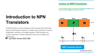
  • 1. Introduction to NPN Transistors An NPN transistor is a type of bipolar junction transistor (BJT) with three layers of semiconductor material. It is widely used in electronic circuits for amplification, switching, and voltage regulation. NPN transistors are crucial components in modern electronics due to their versatility and performance. by VìñåY kumar ECE /024
  • 2. Understanding the basic structure of an NPN transistor Composition An NPN transistor is made of three semiconductor layers: the collector, base, and emitter, where the base is the thinnest layer and the collector is the largest. Doping The semiconductor layers are doped with specific impurities, creating either an excess of electrons (n- type) or a deficiency of electrons (p-type) to form the NPN structure. Function The NPN transistor acts as an amplifier or a switch, controlling the flow of current from the collector to the emitter based on the base current.
  • 3. Key characteristics of NPN transistors Doping Type The NPN transistor is formed by doping the semiconductor material with two types of dopants: one to create a surplus of electrons (N-type) and one to create a deficit (P-type). Current Flow In an NPN transistor, current flows from the collector (C) to the emitter (E) when a small current is applied to the base (B). Amplification NPN transistors are commonly used for signal amplification due to their ability to increase the strength of an input signal. Polarity The NPN transistor is a negatively doped semiconductor placed between two positively doped semiconductors, making it a crucial component in electronic circuits.
  • 4. Collector current (IC) vs. Base current (IB) relationship The relationship between the collector current (IC) and base current (IB) in an NPN transistor is crucial for understanding its behavior. As the base current increases, the collector current also increases, but not linearly. This relationship is key to the amplifier and switching functionalities of NPN transistors.
  • 5. Common Emitter Configuration and Its Significance The common emitter configuration is a key arrangement in NPN transistors, where the emitter is common between the input and output circuits. It provides high voltage gain and medium current gain, making it suitable for use in amplification circuits. This configuration allows for both voltage and current amplification, making it an essential aspect of transistor applications.
  • 6. Voltage gain and current gain of NPN transistors Voltage Gain The voltage gain of an NPN transistor is the ratio of the change in output voltage to the change in input voltage. Current Gain Current gain, often denoted by hfe, refers to the ratio of output current to the input current in an NPN transistor.
  • 7. Biasing Techniques for NPN Transistors Base Biasing Connect a resistor between the base and the positive supply voltage for a simple biasing technique. Collector Feedback Biasing Use the collector-to-base feedback resistor to stabilize the operating point of the NPN transistor. Emitter Biasing Directly connecting the emitter to the ground offers another effective biasing method for NPN transistors.
  • 8. Load line analysis for NPN transistors 1 Understanding Load Line Graphical representation of transistor operation 2 DC Load Line Shows transistor's active region for given collector current 3 AC Load Line Depicts transistor's behavior under AC signal conditions
  • 9. Designing a Circuit for NPN Transistor Characteristics Functionality The circuit should accurately measure key characteristics such as current gain and voltage gain. Components Selection of appropriate resistors, capacitors, and power supply to ensure accurate measurements. Biasing Consider biasing techniques to ensure the transistor operates in the active region for reliable results. Load Line Analyze load line for proper transistor operation and efficient circuit design.
  • 10. Conclusion and key takeaways NPN transistors: Versatile and widely used in electronic circuits Amplification: Ability to amplify current and voltage signals Biasing techniques: Crucial for stable and efficient transistor operation Load line analysis: Important for understanding transistor behavior
  • 11. Introduction to PNP Transistors A PNP transistor is a three-layer semiconductor device that can amplify or switch electronic signals. It consists of a layer of N-doped semiconductor between two layers of P-doped material. When a small current flows into the base of the transistor, it allows a larger current to flow between the collector and emitter. PNP transistors are commonly used in amplification and switching applications. by VìñåY kumar ECE /024
  • 12. Basic Characteristics of PNP Transistors PNP transistors are composed of three layers of semiconductor material: P-type (positive), N-type (negative), and P-type. They operate by allowing a small current to control a much larger one, making them suitable for amplification and switching applications. These transistors require a small base current to turn ON, and the collector current flows from emitter to collector when they are forward- biased. Understanding their characteristics is crucial for designing and fabricating circuits.
  • 13. Circuit fabrication process for PNP transistors 1 Selection of Transistor Type Choose a PNP transistor suitable for the circuit's voltage and current requirements. 2 Positioning on Breadboard Place the PNP transistor securely on the breadboard, ensuring correct pin alignment. 3 Connecting Base, Collector, and Emitter Connect the base, collector, and emitter of the PNP transistor to the appropriate components.
  • 14. Selection of Appropriate Components for the Circuit PNP Transistor Choose a PNP transistor with the appropriate voltage and current ratings for the circuit. Resistors and Capacitors Select resistors and capacitors that match the required values and power ratings. Power Supply Ensure a stable power supply that meets the voltage and current requirements of the circuit.
  • 15. Soldering and connecting the components When soldering the components, ensure the proper placement and connection. Clean and tin the soldering iron, and then carefully solder each connection. Use a multimeter to check for short circuits and verify the continuity of the connections.
  • 16. Testing the Circuit for Functionality Power Supply Compatibility Ensure that the power supply voltage and current are within the specified range for the PNP transistor circuit. Signal Amplification Verify that the PNP transistor is amplifying the input signal as intended, with minimal distortion or noise. Temperature Stability Check for temperature stability to ensure that the circuit performs consistently under varying thermal conditions. Load Handling Capability Test the ability of the PNP transistor circuit to handle the specified load without overheating or malfunctioning.
  • 17. Troubleshooting Common Issues in PNP Transistor Circuits No Output Signal If there is no output signal, check for loose connections and ensure the transistor is properly biased. Overheating Overheating may occur due to excessive current. Review the current flow and the transistor's heat dissipation capabilities. Reverse Polarity If the circuit is not functioning, verify that the PNP transistor is correctly oriented according to the circuit diagram. Base-Emitter Short Avoid a base-emitter short by ensuring the proper voltage and current limits are maintained within the transistor.
  • 18. Understanding the voltage and current requirements Parameter Voltage (V) Current (A) Collector-Emitter Usually negative Varies based on load Base-Emitter 0.6 to 0.7 Small leakage current Base-Collector More negative than emitter Negligible
  • 19. Analyzing the performance of the fabricated circuit 1 Power Consumption Measure the power used by the circuit 2 Signal Amplification Check if the transistor is amplifying the signal as expected 3 Heat Dissipation Monitor the heat dissipation to ensure the circuit's safety After fabricating the circuit, it is crucial to analyze its performance. Firstly, measure the power consumption to ensure efficiency. Secondly, assess the signal amplification capability of the PNP transistor. Finally, monitor heat dissipation to avoid overheating and ensure safe operation.
  • 20. Conclusion and key takeaways 3 Efficient 100K Gain After analyzing the performance of the fabricated circuit, it is evident that an efficient gain of 100K can be achieved.