SlideShare a Scribd company logo
1 of 71
Field-effect transistors
Dr.R.P.Rao
Gate
JFET
Source Drain
Field-effect transistors
Dr.R.P.Rao
Gate
Source Drain
* A Field-Effect Transistor(FET) has a gate (G) terminal w hich controls the
current flow between the other two terminals, viz., source (S) and drain (D).
Field-effect transistors
Dr.R.P.Rao
Gate
Source Drain
* A Field-Effect Transistor(FET) has a gate (G) terminal w hich controls the
current flow between the other two terminals, viz., source (S) and drain (D).
* In simple terms, a FET can be thought of as a resistance connected between S
and D, w hich is a function of the gate voltage VG .
* The mechanism of gate controlvaries in different types of FETs, e.g., JFET,
MESFET, MOSFET, HEMT.
* FETs can be used for analog and digital applications. In each case, the fact that
the gate is used to controlcurrent flow between S and D plays a crucialrole.
Junction Field-effect transistors (JFET)
Dr.R.P.Rao
3D v iew
Gate
Source Drain
Z
L′
G
p+
S D
G L
(Not drawn to scale. Typically, L≫ 2a.)
Cross−sectional v iew
G
p+
S D
G L
Simplified structure
n −Si
2a
n −Si
2a
Junction Field-effect transistors (JFET)
Dr.R.P.Rao
3D v iew
* The n-type region betw een the top and bottom p+
regions offers a resistanceto
current flow. The resistance depends on VG .
* We w ill first consider the case, VD =VS =0 V.
Gate
Source Drain
Z
L′
G
p+
S D
G L
(Not drawn to scale. Typically, L≫ 2a.)
Cross−sectional v iew
G
p+
S D
G L
Simplified structure
n −Si
2a
n −Si
2a
JFET with VS = VD = 0V
Dr.R.P.Rao
a
neutral
depleted G p+
W
S h D
0 V 0V
G L
Vtt = 0 V Vtt =−1 V Vtt = −2 V
G
S
0V
D
0 V
G
G
S
0V
D
0 V
G
JFET with VS = VD = 0V
Dr.R.P.Rao
a
neutral
depleted G p+
W
S h D
0 V 0V
G L
Vtt = 0 V Vtt =−1 V Vtt = −2 V
* The bias across the p-n junction is (VG − VS ), i.e., VG , since VS = VD = 0 V .
G
S
0V
D
0 V
G
G
S
0V
D
0 V
G
JFET with VS = VD = 0V
Dr.R.P.Rao
a
neutral
depleted G p+ G
W
S h D S
G
D S D
0 V 0 V 0 V 0 V 0 V 0 V
G L
Vtt = 0 V
G
Vtt =−1 V
G
Vtt = −2 V
* The bias across the p-n junction is (VG − VS ), i.e., VG , since VS = VD = 0V.
* As the reverse bias across the junction is increased (by making VG more
negative), the depletion region w idens, and the resistance offered by the n-region
increases.
* When the reverse bias becomes large enough, the depletion region consumes the
entire n-region. The corresponding VG is called the “pinch-off” voltage.
JFET: pinch-off voltage
Dr.R.P.Rao
neutral
G
depleted p+
W
S
a
h D
0 V 0V
G
JFET: pinch-off voltage
Dr.R.P.Rao
* VP = VG for w hich h = 0, i.e., W =a.
neutral
depleted
G
p+
W
S
0V
a
h D
0V
G
JFET: pinch-off voltage
Dr.R.P.Rao
s
* VP =VG for w hich h = 0, i.e., W = a.
* For a p+
-n junction, W =
2 s (Vbi − V )
, w here V
q Nd
bi is the built-in potential of
the junction.
neutral
depleted
G
p+
W
S
0V
a
h D
0V
G
JFET: pinch-off voltage
Dr.R.P.Rao
s
s
* VP =VG for w hich h = 0, i.e., W = a.
* For a p+
-n junction, W =
2 s (Vbi − V )
, w here V
q Nd
bi is the built-in potential of
the junction.
* For pinch-off, W =a =
2 s (Vbi − V )
q Nd
⇒ VP = Vbi −
q Nd a2
.
2 s
neutral
depleted
G
p+
W
S
0V
a
h D
0V
G
JFET: pinch-off voltage
Dr.R.P.Rao
neutral
G
depleted p+
W
S
a
h D
0 V 0V
G
JFET: pinch-off voltage
Dr.R.P.Rao
* For pinch-off, W = a =
2 s (Vbi − V )
q Nd
⇒ VP = Vbi −
q Nd a2
.
2 s
neutral
depleted
G
p+
W
S
0V
a
h D
0V
G
s
JFET: pinch-off voltage
Dr.R.P.Rao
* For pinch-off, W = a =
2 s (Vbi − V )
q Nd
⇒ VP = Vbi −
q Nd a2
.
2 s
* Example: Nd = 2 × 10¹⁵
cm−3
, a = 1.5 µm, Vbi = 0.8 V .
neutral
depleted
G
p+
W
S
0V
a
h D
0V
G
s
JFET: pinch-off voltage
Dr.R.P.Rao
* For pinch-off, W = a =
2 s (Vbi − V )
q Nd
⇒ VP = Vbi −
q Nd a2
.
2 s
* Example: Nd = 2 × 10¹⁵
cm−3
, a = 1.5 µm, Vbi = 0.8 V .
(1.6 × 10⁻¹⁹
Coul)(2 × 10¹⁵
cm−3
)((1.5 × 10⁻⁴
)2
cm2
)
W = 0.8 −
2 × 11.7 × 8.85 × 10−14 F/cm
= 0.8 − 3.48 ≈ −2.7 V .
neutral
depleted
G
p+
W
S
0V
a
h D
0V
G
s
JFET: pinch-off voltage
Dr.R.P.Rao
⇒ −
* For pinch-off, W = a =
2 s (Vbi − V )
q Nd
⇒ VP = Vbi −
q Nd a2
.
2 s
* Example: Nd = 2 × 10¹⁵
cm−3
, a = 1.5 µm, Vbi = 0.8 V .
(1.6 × 10⁻¹⁹
Coul)(2 × 10¹⁵
cm−3
)((1.5 × 10⁻⁴
)2
cm2
)
W = 0.8 −
2 × 11.7 × 8.85 × 10−14 F/cm
= 0.8 − 3.48 ≈ −2.7 V .
If a gate voltage VG = 2.7 V is applied, the n-channelgets pinched off, and
the device resistance becomes very large.
neutral
depleted
G
p+
W
S
0V
a
h D
0V
G
s
JFET with VG = constant, VD ƒ= 0V
Dr.R.P.Rao
a
neutral
depleted G p+
W
S h D
0 V
G L
x
G
S
0V
D
G
G
S
0V
D
G
V (x) 1V
0V
ha
W
VD = 1 VVD = 0.05 VVD = 0 V
JFET with VG = constant, VD ƒ= 0V
Dr.R.P.Rao
haha
W
neutral
depleted G p+ G
W
S D S
0 V 0 V
G L G
x
G
D S D
0 V
G
V (x) 1 V
0 V
* Consider an n-JFET w ith VG constant (and not in pinch-off mode).
VD = 1 VVD = 0.05 VVD = 0 V
JFET with VG = constant, VD ƒ= 0V
Dr.R.P.Rao
haha
W
neutral
depleted G p+ G
W
S D S
0 V 0 V
G L G
x
G
D S D
0 V
G
V (x) 1 V
0 V
* Consider an n-JFET w ith VG constant (and not in pinch-off mode).
If a positive VD is applied, the potential V (x ) inside the channelfrom S to D
(along the dashed line) increases from0 Vto VD .
Note that W and h are now functions of x such that, W (x ) + h(x ) = a.
VD = 1 VVD = 0.05 VVD = 0 V
JFET with VG = constant, VD ƒ= 0V
Dr.R.P.Rao
haha
−
W
neutral
depleted G p+ G
W
S D S
0 V 0 V
G L G
x
G
D S D
0 V
G
V (x) 1 V
0 V
* Consider an n-JFET w ith VG constant (and not in pinch-off mode).
If a positive VD is applied, the potential V (x ) inside the channelfrom S to D
(along the dashed line) increases from0 Vto VD .
Note that W and h are now functions of x such that, W (x ) + h(x ) = a.
* Since the p-n junction bias at a given x is (VG V (x )), the drain end of the
channelhas a larger reverse bias than the source end.
VD = 1 VVD = 0.05 VVD = 0 V
JFET with VG = constant, VD ƒ= 0V
Dr.R.P.Rao
⇒ the depletion region is w ider at the drain.
JFET: derivation of ID equation
Dr.R.P.Rao
ha
y G
S D
2 h
0 V
Z
G
V VD
Area = 2 h Z
0 V L x
W
x
JFET: derivation of ID equation
Dr.R.P.Rao
ha
y G
S D
2 h
0 V
Z
G
V VD
Area = 2 h Z
0 V L x
Consider a slice of the dev ice. The current density at any point in the neutral region is assumed to
be in the x direction, and giv en by ,
dn dV
Jn = qµnnE + qDn
dx
≈ qµnnE = qµnNd
dx
,
W
x
JFET: derivation of ID equation
Dr.R.P.Rao
ha
y G
S D
2 h
0 V
Z
G
V VD
Area = 2 h Z
0 V L x
Consider a slice of the dev ice. The current density at any point in the neutral region is assumed to
be in the x direction, and giv en by ,
dn dV
Jn = qµnnE + qDn
dx
≈ qµnnE = qµnNd
dx
,
dn
where we hav e neglected the dif f usion current, since n ≈ Nd ⇒
dx
= 0.
Note that only the neutral part of the n-Si conducts since there are no carriers in the depletion
regions.
At a given x, the current ID is obtained by integrating Jn ov er the area of the neutral channel
region (see f igure on the right). Since Jn is constant ov er this area,
W
x
JFET: derivation of ID equation
Dr.R.P.Rao
ha
D n n d
dx
n d
dx a
y G
S D
2 h
0 V
Z
G
V VD
Area = 2 h Z
0 V L x
Consider a slice of the dev ice. The current density at any point in the neutral region is assumed to
be in the x direction, and giv en by ,
dn dV
Jn = qµnnE + qDn
dx
≈ qµnnE = qµnNd
dx
,
dn
where we hav e neglected the dif f usion current, since n ≈ Nd ⇒
dx
= 0.
Note that only the neutral part of the n-Si conducts since there are no carriers in the depletion
regions.
At a given x, the current ID is obtained by integrating Jn ov er the area of the neutral channel
region (see f igure on the right). Since Jn is constant ov er this area,
I (x ) =
Z Z
J dx dz = 2hZ ×
„
qµ N
dV
«
= 2qZ µ N a
dV
„
1 −
W
«
,
W
x
JFET: derivation of ID equation
Dr.R.P.Rao
where we hav e used h = a − W , i.e., h = a(1 − W /a).
JFET: derivation of ID equation
Dr.R.P.Rao
ha
«
a
y G
dV
ID (x ) = 2 q Z µn Nd a
dx
S D
0 V
„
1 −
W
.
W
x
G
JFET: derivation of ID equation
Dr.R.P.Rao
ha
«
s
Vbi − (VG − V )
a
y G
dV
ID (x ) = 2 q Z µn Nd a
dx
S D
0 V
„
1 −
W
.
Since ID (x ) is constant f rom x = 0 to x = L, we get,
Z L Z VD
s
2s
q !
where we hav e used, f or the depletion width W ,
W (x ) =
2s
qNd
[Vbi − (VG − V )] .
qNd a2
00
IDdx = ID L = 2qZ µnNd a
W
x
1 − dV ,
G
JFET: derivation of ID equation
Dr.R.P.Rao
ha
«
s
Vbi − (VG − V )
VD −
3
(Vbi − VP )
a
y G
dV
ID (x ) = 2 q Z µn Nd a
dx
S D
0 V
„
1 −
W
.
Since ID (x ) is constant f rom x = 0 to x = L, we get,
Z L Z VD
s
2s
q !
where we hav e used, f or the depletion width W ,
W (x ) =
2s
qNd
[Vbi − (VG − V )] .
qNd a2
Ev aluating the integral and using Vbi − VP = , we get (do this!)
2s
(
2
"„
VD + Vbi − VG
«3/2 „
Vbi − VG
«3/2
#)
where G0 = 2qZ µnNd a/L.
PbiVPbiV
qNd a2
00
IDdx = ID L = 2qZ µnNd a
W
x
1 − dV ,
ID = G0
− V
−
− V
,
G
JFET: derivation of ID equation
ha
«
s
Vbi − (VG − V )
VD −
3
(Vbi − VP )
a
y G
dV
ID (x ) = 2 q Z µn Nd a
dx
S D
0 V
„
1 −
W
.
Since ID (x ) is constant f rom x = 0 to x = L, we get,
Z L Z VD
s
2s
q !
where we hav e used, f or the depletion width W ,
W (x ) =
2s
qNd
[Vbi − (VG − V )] .
qNd a2
Ev aluating the integral and using Vbi − VP = , we get (do this!)
2s
(
2
"„
VD + Vbi − VG
«3/2 „
Vbi − VG
«3/2
#)
where G0 = 2qZ µnNd a/L.
Note that G0 is the channel conductance if there was no depletion, i.e., if h(x ) = a throughout the
channel.
PbiVPbiV
qNd a2
00
IDdx = ID L = 2qZ µnNd a
W
x
1 − dV ,
ID = G0
− V
−
− V
,
G
Special case: VD ≈ 0V
Dr.R.P.Rao
VD ≈ 0 V
a
VD −
3
(Vbi − VP )
neutral
depleted G p+
W
S h D
0 V
G L
(
2
"„
VD + Vbi − VG
«3/2
„
Vbi − VG
/2
#)
PbiVPbiV
y G
S
0V
D
G
x
ha
W
ID = G0
− V
−
− V
Special case: VD ≈ 0V
Dr.R.P.Rao
VD ≈ 0 V
a
VD −
3
(Vbi − VP )
− V − V
0
3 P
2
bi G
neutral
depleted G p+
W
S h D
0 V
G L
(
2
"„
VD + Vbi − VG
«3/2
„
Vbi − VG
«3/2
#)
≈ G V
2
− (V − V )−1/2
»
3
V (V − V )1/2
–ff
(using Taylor’s series)
PbiVPbiV
y G
S
0V
D
G
x
ha
W
ID = G0 −
D
bi D
Special case: VD ≈ 0V
Dr.R.P.Rao
VD ≈ 0 V
a
VD −
3
(Vbi − VP )
− V − V
0
3
P
2 bi G
1 −
Vbi P
neutral
depleted G p+
W
S h D
0 V
G L
(
2
"„
VD + Vbi − VG
«3/2
„
Vbi − VG
«3/2
#)
≈ G V
2
− (V − V )−1/2
»
3
V (V − V )1/2
–ff
(using Taylor’s series)
( „
Vbi − VG
«1/2
)
PbiVPbiV
y G
S
0V
D
G
x
ha
W
ID = G0 −
D bi D
= G0VD
− V
.
Special case: VD ≈ 0V
Dr.R.P.Rao
VD ≈ 0 V
a
1/2
VD −
3
(Vbi − VP )
− V − V
0
3
P
2 bi G
1 −
Vbi P
neutral
depleted G p+
W
S h D
0 V
G L
(
2
"„
VD + Vbi − VG
«3/2
„
Vbi − VG
«3/2
#)
≈ G V
2
− (V − V )−1/2
»
3
V (V − V )1/2
–ff
(using Taylor’s series)
( „
Vbi − VG
«1/2
)
2sSince W = (V
1/2 2s
− V ) , and a = (V
− V ) , we get
bi G
qNd
bi P
qNd
PbiVPbiV
y G
S
0V
D
G
x
ha
W
ID = G0 −
D bi D
= G0VD
− V
.
Special case: VD ≈ 0V
VD ≈ 0 V
a
1/2
a
VD −
3
(Vbi − VP )
− V − V
0
3
P
2 bi G
1 −
Vbi P
neutral
depleted G p+
W
S h D
0 V
G L
(
2
"„
VD + Vbi − VG
«3/2
„
Vbi − VG
«3/2
#)
≈ G V
2
− (V − V )−1/2
»
3
V (V − V )1/2
–ff
(using Taylor’s series)
( „
Vbi − VG
«1/2
)
2sSince W = (V
1/2 2s
− V ) , and a = (V
− V ) , we get
bi G
qNd
bi P
qNd
ID = G0VD 1 −
W
f f
.
This simply shows that the channel conductance reduces linearly with W (as seen bef ore the
VS = VS = 0 V condition), and f or VG = VP (i.e., W = a), the conductance becomes zero.
PbiVPbiV
y G
S
0V
D
G
x
ha
W
ID = G0 −
D bi D
= G0VD
− V
.
JFET: pinch-off near drain
VD −
3
(Vbi − VP )
200
150
100
50
0
0
(
2
"„
VD + Vbi − VG
«3/2
1 2 3 4 5
VD (Volts)
„
Vbi − VG
«3/2
#)
PbiVPbiV
y G
S
0 V
D
G
x
h
a
W
Vtt =0 V
Vtt =−1 V
Vtt =−2 V
ID(µA)
ID = G0
− V
−
− V
.
JFET: pinch-off near drain
−
VD −
3
(Vbi − VP )
200
150
100
50
0
0
(
2
"„
VD + Vbi − VG
«3/2
1 2 3 4 5
VD (Volts)
„
Vbi − VG
«3/2
#)
For a giv en VG , ID reaches a maximum at VD = VG VP (show this by dif f erentiating the abov e
equation).
At this v alue of VD , the bias across the p-n junction at the drain end is VG − VD = VP .
PbiVPbiV
y G
S
0 V
D
G
x
h
a
W
Vtt =0 V
Vtt =−1 V
Vtt =−2 V
ID(µA)
ID = G0
− V
−
− V
.
JFET: pinch-off near drain
−
−
VD −
3
(Vbi − VP )
200
150
100
50
0
0
(
2
"„
VD + Vbi − VG
«3/2
1 2 3 4 5
VD (Volts)
„
Vbi − VG
«3/2
#)
For a giv en VG , ID reaches a maximum at VD = VG VP (show this by dif f erentiating the abov e
equation).
At this v alue of VD, the bias across the p-n junction at the drain end is VG VD = VP .
In other words, the drain end of the channel has just reached pinch-of f .
G
S D
0 V pinch−off
G
PbiVPbiV
y G
S
0 V
D
G
x
h
a
W
Vtt =0 V
Vtt =−1 V
Vtt =−2 V
ID(µA)
ID = G0
− V
−
− V
.
JFET: pinch-off near drain
−
−
VD −
3
(Vbi − VP )
200
150
100
50
0
0
(
2
"„
VD + Vbi − VG
«3/2
1 2 3 4 5
VD (Volts)
„
Vbi − VG
«3/2
#)
For a giv en VG , ID reaches a maximum at VD = VG VP (show this by dif f erentiating the abov e
equation).
At this v alue of VD, the bias across the p-n junction at the drain end is VG VD = VP .
In other words, the drain end of the channel has just reached pinch-of f .
G
S
0 V
G
What happens if VD is increased f urther?
D
pinch−off
PbiVPbiV
y G
S
0 V
D
G
x
h
a
W
Vtt =0 V
Vtt =−1 V
Vtt =−2 V
ID(µA)
ID = G0
− V
−
− V
.
JFET: saturation
sat
D
DV < V
D tt
G G G
S D S D S
0V 0V 0V
G
A VD ≈ 0V
G G
B C
ID
C D
B
A
VD
V sat = V − V
Consider a f ixed VG with VD v ary ing f rom ∼ 0 V to a v alue bey ond condition C.
G
D S
0 V
D
G
D sat
D
DV > V
sat
D
DV = V
P
JFET: saturation
sat
D
DV < V
D tt
G G G
S D S D S
0V 0V 0V
G
A VD ≈ 0V
G G
B C
ID
C D
B
A
VD
V sat = V − V
Consider a f ixed VG with VD v ary ing f rom ∼ 0 V to a v alue bey ond condition C.
In this situation, i.e., VD > V sat
, a short high-f ield region dev elops near the drain end, and the
“excess” v oltage, VD
sat
D
− VD drops across this region.
G
D S
0 V
D
G
D sat
D
DV > V
sat
D
DV = V
P
JFET: saturation
sat
D
DV < V
D tt
G G G
S D S D S
0V 0V 0V
G
A VD ≈ 0V
G G
B C
ID
C D
B
A
VD
V sat = V − V
Consider a f ixed VG with VD v ary ing f rom ∼ 0 V to a v alue bey ond condition C.
In this situation, i.e., VD > V sat
, a short high-f ield region dev elops near the drain end, and the
“excess” v oltage, VD
sat
D
− VD drops across this region.
Because the high-f iled region is conf ined to a v ery small distance, the conditions in the dev ice are
almost identical in C and D.
G
D S
0 V
D
G
D sat
D
DV > V
sat
D
DV = V
P
JFET: saturation
sat
D
DV < V
D tt
G G G
S D S D S
0V 0V 0V
G
A VD ≈ 0V
G G
B C
ID
C D
B
A
VD
V sat = V − V
Consider a f ixed VG with VD v ary ing f rom ∼ 0 V to a v alue bey ond condition C.
In this situation, i.e., VD > V sat
, a short high-f ield region dev elops near the drain end, and the
“excess” v oltage, VD
sat
D
− VD drops across this region.
Because the high-f iled region is conf ined to a v ery small distance, the conditions in the dev ice are
almost identical in C and D.
⇒ The current in case D is almost the same as that f or case C.
G
D S
0 V
D
G
D sat
D
DV > V
sat
D
DV = V
P
JFET: saturation
sat
D
DV < V
D
D tt
G G G
S D S D S
0V 0V 0V
G
A VD ≈ 0V
G G
B C
ID
C D
B
A
VD
V sat = V − V
Consider a f ixed VG with VD v ary ing f rom ∼ 0 V to a v alue bey ond condition C.
In this situation, i.e., VD > V sat
, a short high-f ield region dev elops near the drain end, and the
“excess” v oltage, VD
sat
D
− VD drops across this region.
Because the high-f iled region is conf ined to a v ery small distance, the conditions in the dev ice are
almost identical in C and D.
⇒ The current in case D is almost the same as that f or case C.
The region VD > V sat
is theref ore called the “saturation region.”
G
D S
0 V
D
G
D sat
D
DV > V
sat
D
DV = V
P
JFET: example
D
An n-channel silicon JFET has the f ollowing parameters (at T = 300 K ): a = 1.5 µm, L = 5 µm,
Z = 50 µm, Nd = 2 × 10¹⁵
cm− 3
, Vbi = 0.8 V , µn = 300 cm2
/V -sec.
(a) What is the pinch-of f v oltage?
(b) Write a program to generate ID -VD characteristics f or VG = 0 V , −0.5 V , −1 V , −1.5 V ,
−2 V.
(c) For each of the abov e VG v alues, compute V sat
, and show it on the ID -VD plot. The part of
an I -V corresponding to V D
< V sat
D D D D is called the “linear” region, and that corresponding
to VD > V sat
is called the “saturation” region.
Answer:
(a) VP =
(b)
200
150
100
50
0
0 1 2 3 4 5
VD (Volts)
−2.68 V.
linear saturation
Vtt =0 V
−0.5 V
−1 V
−1.5 V
−2 V
ID(µA)
JFET: simplified model for saturation
VD −
3
(Vbi − VP )
(
2
"„
VD + Vbi − VG
«3/2 „
Vbi − VG
«3/2
#)
PbiVPbiVID = G0
− V
−
− V
.
JFET: simplified model for saturation
D
VD −
3
(Vbi − VP )
ID = G0 VD −
3
(Vbi − VP )
(
2
"„
VD + Vbi − VG
«3/2 „
Vbi − VG
«3/2
#)
At saturtation, V sat
= VG − VP , giv ing
sat
(
2 " „
Vbi − VG
«3/2
#)
PbiV
PbiVPbiV
ID = G0
− V
−
− V
.
1 −
− V
.
JFET: simplified model for saturation
D
VD −
3
(Vbi − VP )
ID = G0 VD −
3
(Vbi − VP )
D D
(
2
"„
VD + Vbi − VG
«3/2 „
Vbi − VG
«3/2
#)
At saturtation, V sat
= VG − VP , giv ing
sat
(
2 " „
Vbi − VG
«3/2
#)
The f ollowing approximate model is f ound to be adequate in circuit design:
I sat
(VG ) = IDSS (1 − VG /VP )2
, where IDSS = I sat
(VG = 0 V ).
PbiV
PbiVPbiV
ID = G0
− V
−
− V
.
1 −
− V
.
JFET: simplified model for saturation
D
VD −
3
(Vbi − VP )
ID = G0 VD −
3
(Vbi − VP )
(
2
"„
VD + Vbi − VG
«3/2 „
Vbi − VG
«3/2
#)
At saturtation, V sat
= VG − VP , giv ing
sat
(
2 " „
Vbi − VG
«3/2
#)
The f ollowing approximate model is f ound to be adequate in circuit design:
I sat
(VG ) = IDSS (1 − VG /VP )2
, where IDSS = I sat
(VG = 0 V ).
D
In amplif ier design, we are interested in g
D
∂ID
= , which is obtained as:
G
PbiV
PbiVPbiV
˛
ID = G0
− V
−
− V
.
1 −
− V
.
m
∂V ˛
VD=constant
JFET: simplified model for saturation
D
˛
VD −
3
(Vbi − VP )
ID = G0 VD −
3
(Vbi − VP )
(
2
"„
VD + Vbi − VG
«3/2 „
Vbi − VG
«3/2
#)
At saturtation, V sat
= VG − VP , giv ing
sat
(
2 " „
Vbi − VG
«3/2
#)
The f ollowing approximate model is f ound to be adequate in circuit design:
I sat
(VG ) = IDSS (1 − VG /VP )2
, where IDSS = I sat
(VG = 0 V ).
D
In amplif ier design, we are interested in g
D
∂ID= , which is obtained as:
gm = gm0 (1 − VG /VP ),
m
∂VG
˛
VD =constant
where gm0 = −2IDSS /VP = gm(VG = 0 V ).
PbiV
PbiVPbiV
ID = G0
− V
−
− V
.
1 −
− V
.
JFET: source/drain resistances
S′ D′
G
(Not drawn to scale. Typically, L ≫ 2a.)
Cross−sectional v iew
RS RD
G p+
S D
G L
n −Si
2a
S D
JFET: source/drain resistances
S′ D′
G
(Not drawn to scale. Typically, L ≫ 2a.)
Cro ss − s e ct io n a l view
In real JFETs, there is a separation between the source/drain contacts and the activ e channel.
The n-ty pe semiconductor regions between the activ e channel and the source/drain contacts can
be modelled by resistances RS and RD .
RS RD
G p+
S D
G L
n −Si
2a
S D
JFET: small-signal model
VDD
D R R
D
Vo
1 V2
Rtt
S
S
Rtt
VSS
Amplifier example
* A small-signal model of a JFET is required in analy sis of an amplif ier.
G
vg
Cgd
Cgs gd
gmvg
G
V
JFET: small-signal model
VDD
D R R
D
Vo
1 V2
Rtt
S
S
Rtt
VSS
Amplifier example
* A small-signal model of a JFET is required in analy sis of an amplif ier.
* The DC gate current, which is the rev erse current of a p-n junction, is generally insignif icant
and is theref ore ignored.
G
vg
Cgd
Cgs gd
gmvg
G
V
JFET: small-signal model
VDD
D R R
D
Vo
1 V2
Rtt
S
S
Rtt
VSS
Amplifier example
* A small-signal model of a JFET is required in analy sis of an amplif ier.
* The DC gate current, which is the rev erse current of a p-n junction, is generally insignif icant
and is theref ore ignored.
∂ID
* gm =
∂VG
with VD = constant.
G
vg
Cgd
Cgs gd
gmvg
G
V
JFET: small-signal model
VDD
D R R
D
Vo
1 V2
Rtt
S
S
Rtt
VSS
Amplifier example
* A small-signal model of a JFET is required in analy sis of an amplif ier.
* The DC gate current, which is the rev erse current of a p-n junction, is generally insignif icant
and is theref ore ignored.
∂ID
* gm =
* gd =
∂VG
∂ID
∂VD
with VD = constant.
with VG = constant.
G
vg
Cgd
Cgs gd
gmvg
G
V
JFET: small-signal model
saturation. Howev er, a real dev ice would show a small increase in ID with an increase in VD
in saturation, giv ing rise to a non-zero gd .
VDD
D R R
D
Vo
1 V2
Rtt
S
S
Rtt
VSS
Amplifier example
* A small-signal model of a JFET is required in analy sis of an amplif ier.
* The DC gate current, which is the rev erse current of a p-n junction, is generally insignif icant
and is theref ore ignored.
∂ID
* gm =
* gd =
∂VG
∂ID
∂VD
with VD = constant.
with VG = constant.
* gm and gd can be obtained by dif ferentiating ID (VG , VD ). Note that, in our simple model,
short-channel ef f ects have not been included; we would theref ore obtain gd = 0 ¥ in
G
vg
Cgd
Cgs gd
gmvg
G
V
JFET: small-signal model
saturation. Howev er, a real dev ice would show a small increase in ID with an increase in VD
in saturation, giv ing rise to a non-zero gd .
* The capacitances Cgs and Cgd are depletion capacitances of the p-n junction.
VDD
D R R
D
Vo
1 V2
Rtt
S
S
Rtt
VSS
Amplifier example
* A small-signal model of a JFET is required in analy sis of an amplif ier.
* The DC gate current, which is the rev erse current of a p-n junction, is generally insignif icant
and is theref ore ignored.
∂ID
* gm =
* gd =
∂VG
∂ID
∂VD
with VD = constant.
with VG = constant.
* gm and gd can be obtained by dif ferentiating ID (VG , VD ). Note that, in our simple model,
short-channel ef f ects have not been included; we would theref ore obtain gd = 0 ¥ in
G
vg
Cgd
Cgs gd
gmvg
G
V

More Related Content

What's hot

Electronic devices-and-circuit-theory-10th-ed-boylestad-chapter-8
Electronic devices-and-circuit-theory-10th-ed-boylestad-chapter-8Electronic devices-and-circuit-theory-10th-ed-boylestad-chapter-8
Electronic devices-and-circuit-theory-10th-ed-boylestad-chapter-8
Shiwam Isrie
 
EE20-Chapter 5
EE20-Chapter 5 EE20-Chapter 5
EE20-Chapter 5
ruhiyah
 

What's hot (20)

Electronic devices-and-circuit-theory-10th-ed-boylestad-chapter-8
Electronic devices-and-circuit-theory-10th-ed-boylestad-chapter-8Electronic devices-and-circuit-theory-10th-ed-boylestad-chapter-8
Electronic devices-and-circuit-theory-10th-ed-boylestad-chapter-8
 
FET AMPLIFIER
FET AMPLIFIERFET AMPLIFIER
FET AMPLIFIER
 
Fe ts mosfet
Fe ts mosfetFe ts mosfet
Fe ts mosfet
 
JFET common drain characteristics
JFET common drain characteristicsJFET common drain characteristics
JFET common drain characteristics
 
Common Source Characteristics - JFET
Common Source Characteristics - JFETCommon Source Characteristics - JFET
Common Source Characteristics - JFET
 
Rec101 unit ii (part 3) field effect transistor
Rec101 unit ii (part 3) field effect transistorRec101 unit ii (part 3) field effect transistor
Rec101 unit ii (part 3) field effect transistor
 
Fet
FetFet
Fet
 
EE20-Chapter 5
EE20-Chapter 5 EE20-Chapter 5
EE20-Chapter 5
 
Voltage regulator
Voltage regulatorVoltage regulator
Voltage regulator
 
MOSFET as an Amplifier
MOSFET as an AmplifierMOSFET as an Amplifier
MOSFET as an Amplifier
 
Field Effect Transistor
Field Effect TransistorField Effect Transistor
Field Effect Transistor
 
Stabilization Of Operating Point | Electrical Engineering
Stabilization Of Operating Point | Electrical EngineeringStabilization Of Operating Point | Electrical Engineering
Stabilization Of Operating Point | Electrical Engineering
 
Hybrid model analog electronics
Hybrid model analog electronicsHybrid model analog electronics
Hybrid model analog electronics
 
EE201 -Chapter 4
EE201 -Chapter 4 EE201 -Chapter 4
EE201 -Chapter 4
 
Ppt presentation on FET
Ppt presentation on  FETPpt presentation on  FET
Ppt presentation on FET
 
dc biasing of bjt
dc biasing of bjtdc biasing of bjt
dc biasing of bjt
 
L07 dc and ac load line
L07 dc and ac load lineL07 dc and ac load line
L07 dc and ac load line
 
Field Effect Biasing - Part 1
Field Effect Biasing - Part 1Field Effect Biasing - Part 1
Field Effect Biasing - Part 1
 
Stabilisation
StabilisationStabilisation
Stabilisation
 
dc biasing
dc biasingdc biasing
dc biasing
 

Similar to Fet

Notes 2 5317-6351 Transmission Lines Part 1 (TL Theory).pptx
Notes 2 5317-6351 Transmission Lines Part 1 (TL Theory).pptxNotes 2 5317-6351 Transmission Lines Part 1 (TL Theory).pptx
Notes 2 5317-6351 Transmission Lines Part 1 (TL Theory).pptx
DibyadipRoy1
 
Chapter 4 semiconductor devicee JFET.pdf
Chapter 4 semiconductor devicee JFET.pdfChapter 4 semiconductor devicee JFET.pdf
Chapter 4 semiconductor devicee JFET.pdf
Yohannes427126
 
MOSFET IV characteristics and its operations
MOSFET IV characteristics and its operationsMOSFET IV characteristics and its operations
MOSFET IV characteristics and its operations
jpradha86
 

Similar to Fet (20)

Field Effect Transistor (FET)
Field Effect Transistor (FET)Field Effect Transistor (FET)
Field Effect Transistor (FET)
 
Introduction to Junction Field Effect Transistor
Introduction to Junction Field Effect TransistorIntroduction to Junction Field Effect Transistor
Introduction to Junction Field Effect Transistor
 
FET lecture_Electronics by Arif Sir
FET lecture_Electronics by Arif SirFET lecture_Electronics by Arif Sir
FET lecture_Electronics by Arif Sir
 
Notes 2 5317-6351 Transmission Lines Part 1 (TL Theory).pptx
Notes 2 5317-6351 Transmission Lines Part 1 (TL Theory).pptxNotes 2 5317-6351 Transmission Lines Part 1 (TL Theory).pptx
Notes 2 5317-6351 Transmission Lines Part 1 (TL Theory).pptx
 
Transmission Lines Part 1 (TL Theory).pptx
Transmission Lines Part 1 (TL Theory).pptxTransmission Lines Part 1 (TL Theory).pptx
Transmission Lines Part 1 (TL Theory).pptx
 
Field Effect Transistor
Field Effect Transistor Field Effect Transistor
Field Effect Transistor
 
Session 2
Session 2Session 2
Session 2
 
Chapter 4 semiconductor devicee JFET.pdf
Chapter 4 semiconductor devicee JFET.pdfChapter 4 semiconductor devicee JFET.pdf
Chapter 4 semiconductor devicee JFET.pdf
 
AE UNIT IV.ppt
AE UNIT IV.pptAE UNIT IV.ppt
AE UNIT IV.ppt
 
Lec-2.pdf
Lec-2.pdfLec-2.pdf
Lec-2.pdf
 
Lec-2.pdf
Lec-2.pdfLec-2.pdf
Lec-2.pdf
 
IDS MOS Equation (1).pptx
IDS MOS Equation (1).pptxIDS MOS Equation (1).pptx
IDS MOS Equation (1).pptx
 
fet ppt.pptx
fet ppt.pptxfet ppt.pptx
fet ppt.pptx
 
2006 devmodel
2006 devmodel2006 devmodel
2006 devmodel
 
Lecture08
Lecture08Lecture08
Lecture08
 
Topic 2b ac_circuits_analysis
Topic 2b ac_circuits_analysisTopic 2b ac_circuits_analysis
Topic 2b ac_circuits_analysis
 
16148_jfet1.ppt
16148_jfet1.ppt16148_jfet1.ppt
16148_jfet1.ppt
 
B02010711
B02010711B02010711
B02010711
 
MOSFET.ppt
MOSFET.pptMOSFET.ppt
MOSFET.ppt
 
MOSFET IV characteristics and its operations
MOSFET IV characteristics and its operationsMOSFET IV characteristics and its operations
MOSFET IV characteristics and its operations
 

More from Prakash Rao (20)

PAL
PALPAL
PAL
 
Digital Signal Processing by Dr. R. Prakash Rao
Digital Signal Processing by Dr. R. Prakash Rao Digital Signal Processing by Dr. R. Prakash Rao
Digital Signal Processing by Dr. R. Prakash Rao
 
Electromagnetic Theory and Transmission Lines by Dr. R. Prakash Rao
Electromagnetic Theory and Transmission Lines  by Dr. R. Prakash RaoElectromagnetic Theory and Transmission Lines  by Dr. R. Prakash Rao
Electromagnetic Theory and Transmission Lines by Dr. R. Prakash Rao
 
VLSI15
VLSI15VLSI15
VLSI15
 
VLSI14
VLSI14VLSI14
VLSI14
 
VLSI13
VLSI13VLSI13
VLSI13
 
VLSI12
VLSI12VLSI12
VLSI12
 
VLSI11
VLSI11VLSI11
VLSI11
 
VLSI9
VLSI9VLSI9
VLSI9
 
VLSI8
VLSI8VLSI8
VLSI8
 
VLSI7
VLSI7VLSI7
VLSI7
 
VLSI6
VLSI6VLSI6
VLSI6
 
VLSI5
VLSI5VLSI5
VLSI5
 
VLSI4
VLSI4VLSI4
VLSI4
 
VLSI3
VLSI3VLSI3
VLSI3
 
VLSI2
VLSI2VLSI2
VLSI2
 
VLSI DESIGN
VLSI DESIGN VLSI DESIGN
VLSI DESIGN
 
VLSI10
VLSI10VLSI10
VLSI10
 
BIASING OF BJT
BIASING OF BJT BIASING OF BJT
BIASING OF BJT
 
Diode and its Applications
Diode and its Applications Diode and its Applications
Diode and its Applications
 

Recently uploaded

Cara Menggugurkan Sperma Yang Masuk Rahim Biyar Tidak Hamil
Cara Menggugurkan Sperma Yang Masuk Rahim Biyar Tidak HamilCara Menggugurkan Sperma Yang Masuk Rahim Biyar Tidak Hamil
Cara Menggugurkan Sperma Yang Masuk Rahim Biyar Tidak Hamil
Cara Menggugurkan Kandungan 087776558899
 
Call Girls In Bangalore ☎ 7737669865 🥵 Book Your One night Stand
Call Girls In Bangalore ☎ 7737669865 🥵 Book Your One night StandCall Girls In Bangalore ☎ 7737669865 🥵 Book Your One night Stand
Call Girls In Bangalore ☎ 7737669865 🥵 Book Your One night Stand
amitlee9823
 
VIP Call Girls Ankleshwar 7001035870 Whatsapp Number, 24/07 Booking
VIP Call Girls Ankleshwar 7001035870 Whatsapp Number, 24/07 BookingVIP Call Girls Ankleshwar 7001035870 Whatsapp Number, 24/07 Booking
VIP Call Girls Ankleshwar 7001035870 Whatsapp Number, 24/07 Booking
dharasingh5698
 
Standard vs Custom Battery Packs - Decoding the Power Play
Standard vs Custom Battery Packs - Decoding the Power PlayStandard vs Custom Battery Packs - Decoding the Power Play
Standard vs Custom Battery Packs - Decoding the Power Play
Epec Engineered Technologies
 
notes on Evolution Of Analytic Scalability.ppt
notes on Evolution Of Analytic Scalability.pptnotes on Evolution Of Analytic Scalability.ppt
notes on Evolution Of Analytic Scalability.ppt
MsecMca
 

Recently uploaded (20)

Cara Menggugurkan Sperma Yang Masuk Rahim Biyar Tidak Hamil
Cara Menggugurkan Sperma Yang Masuk Rahim Biyar Tidak HamilCara Menggugurkan Sperma Yang Masuk Rahim Biyar Tidak Hamil
Cara Menggugurkan Sperma Yang Masuk Rahim Biyar Tidak Hamil
 
Call Girls In Bangalore ☎ 7737669865 🥵 Book Your One night Stand
Call Girls In Bangalore ☎ 7737669865 🥵 Book Your One night StandCall Girls In Bangalore ☎ 7737669865 🥵 Book Your One night Stand
Call Girls In Bangalore ☎ 7737669865 🥵 Book Your One night Stand
 
Thermal Engineering Unit - I & II . ppt
Thermal Engineering  Unit - I & II . pptThermal Engineering  Unit - I & II . ppt
Thermal Engineering Unit - I & II . ppt
 
Minimum and Maximum Modes of microprocessor 8086
Minimum and Maximum Modes of microprocessor 8086Minimum and Maximum Modes of microprocessor 8086
Minimum and Maximum Modes of microprocessor 8086
 
KubeKraft presentation @CloudNativeHooghly
KubeKraft presentation @CloudNativeHooghlyKubeKraft presentation @CloudNativeHooghly
KubeKraft presentation @CloudNativeHooghly
 
VIP Call Girls Ankleshwar 7001035870 Whatsapp Number, 24/07 Booking
VIP Call Girls Ankleshwar 7001035870 Whatsapp Number, 24/07 BookingVIP Call Girls Ankleshwar 7001035870 Whatsapp Number, 24/07 Booking
VIP Call Girls Ankleshwar 7001035870 Whatsapp Number, 24/07 Booking
 
Call Girls Pimpri Chinchwad Call Me 7737669865 Budget Friendly No Advance Boo...
Call Girls Pimpri Chinchwad Call Me 7737669865 Budget Friendly No Advance Boo...Call Girls Pimpri Chinchwad Call Me 7737669865 Budget Friendly No Advance Boo...
Call Girls Pimpri Chinchwad Call Me 7737669865 Budget Friendly No Advance Boo...
 
University management System project report..pdf
University management System project report..pdfUniversity management System project report..pdf
University management System project report..pdf
 
Work-Permit-Receiver-in-Saudi-Aramco.pptx
Work-Permit-Receiver-in-Saudi-Aramco.pptxWork-Permit-Receiver-in-Saudi-Aramco.pptx
Work-Permit-Receiver-in-Saudi-Aramco.pptx
 
Design For Accessibility: Getting it right from the start
Design For Accessibility: Getting it right from the startDesign For Accessibility: Getting it right from the start
Design For Accessibility: Getting it right from the start
 
DC MACHINE-Motoring and generation, Armature circuit equation
DC MACHINE-Motoring and generation, Armature circuit equationDC MACHINE-Motoring and generation, Armature circuit equation
DC MACHINE-Motoring and generation, Armature circuit equation
 
VIP Model Call Girls Kothrud ( Pune ) Call ON 8005736733 Starting From 5K to ...
VIP Model Call Girls Kothrud ( Pune ) Call ON 8005736733 Starting From 5K to ...VIP Model Call Girls Kothrud ( Pune ) Call ON 8005736733 Starting From 5K to ...
VIP Model Call Girls Kothrud ( Pune ) Call ON 8005736733 Starting From 5K to ...
 
ONLINE FOOD ORDER SYSTEM PROJECT REPORT.pdf
ONLINE FOOD ORDER SYSTEM PROJECT REPORT.pdfONLINE FOOD ORDER SYSTEM PROJECT REPORT.pdf
ONLINE FOOD ORDER SYSTEM PROJECT REPORT.pdf
 
Hazard Identification (HAZID) vs. Hazard and Operability (HAZOP): A Comparati...
Hazard Identification (HAZID) vs. Hazard and Operability (HAZOP): A Comparati...Hazard Identification (HAZID) vs. Hazard and Operability (HAZOP): A Comparati...
Hazard Identification (HAZID) vs. Hazard and Operability (HAZOP): A Comparati...
 
Standard vs Custom Battery Packs - Decoding the Power Play
Standard vs Custom Battery Packs - Decoding the Power PlayStandard vs Custom Battery Packs - Decoding the Power Play
Standard vs Custom Battery Packs - Decoding the Power Play
 
notes on Evolution Of Analytic Scalability.ppt
notes on Evolution Of Analytic Scalability.pptnotes on Evolution Of Analytic Scalability.ppt
notes on Evolution Of Analytic Scalability.ppt
 
Unleashing the Power of the SORA AI lastest leap
Unleashing the Power of the SORA AI lastest leapUnleashing the Power of the SORA AI lastest leap
Unleashing the Power of the SORA AI lastest leap
 
(INDIRA) Call Girl Aurangabad Call Now 8617697112 Aurangabad Escorts 24x7
(INDIRA) Call Girl Aurangabad Call Now 8617697112 Aurangabad Escorts 24x7(INDIRA) Call Girl Aurangabad Call Now 8617697112 Aurangabad Escorts 24x7
(INDIRA) Call Girl Aurangabad Call Now 8617697112 Aurangabad Escorts 24x7
 
A Study of Urban Area Plan for Pabna Municipality
A Study of Urban Area Plan for Pabna MunicipalityA Study of Urban Area Plan for Pabna Municipality
A Study of Urban Area Plan for Pabna Municipality
 
Double Revolving field theory-how the rotor develops torque
Double Revolving field theory-how the rotor develops torqueDouble Revolving field theory-how the rotor develops torque
Double Revolving field theory-how the rotor develops torque
 

Fet

  • 2. Field-effect transistors Dr.R.P.Rao Gate Source Drain * A Field-Effect Transistor(FET) has a gate (G) terminal w hich controls the current flow between the other two terminals, viz., source (S) and drain (D).
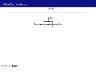
  • 3. Field-effect transistors Dr.R.P.Rao Gate Source Drain * A Field-Effect Transistor(FET) has a gate (G) terminal w hich controls the current flow between the other two terminals, viz., source (S) and drain (D). * In simple terms, a FET can be thought of as a resistance connected between S and D, w hich is a function of the gate voltage VG .
  • 4. Field-effect transistors Dr.R.P.Rao Gate Source Drain * A Field-Effect Transistor(FET) has a gate (G) terminal w hich controls the current flow between the other two terminals, viz., source (S) and drain (D). * In simple terms, a FET can be thought of as a resistance connected between S and D, w hich is a function of the gate voltage VG . * The mechanism of gate controlvaries in different types of FETs, e.g., JFET, MESFET, MOSFET, HEMT.
  • 5. Field-effect transistors Dr.R.P.Rao Gate Source Drain * A Field-Effect Transistor(FET) has a gate (G) terminal w hich controls the current flow between the other two terminals, viz., source (S) and drain (D). * In simple terms, a FET can be thought of as a resistance connected between S and D, w hich is a function of the gate voltage VG . * The mechanism of gate controlvaries in different types of FETs, e.g., JFET, MESFET, MOSFET, HEMT. * FETs can be used for analog and digital applications. In each case, the fact that the gate is used to controlcurrent flow between S and D plays a crucialrole.
  • 6. Junction Field-effect transistors (JFET) Dr.R.P.Rao 3D v iew Gate Source Drain Z L′ G p+ S D G L (Not drawn to scale. Typically, L≫ 2a.) Cross−sectional v iew G p+ S D G L Simplified structure n −Si 2a n −Si 2a
  • 7. Junction Field-effect transistors (JFET) Dr.R.P.Rao 3D v iew * The n-type region betw een the top and bottom p+ regions offers a resistanceto current flow. The resistance depends on VG . Gate Source Drain Z L′ G p+ S D G L (Not drawn to scale. Typically, L≫ 2a.) Cross−sectional v iew G p+ S D G L Simplified structure n −Si 2a n −Si 2a
  • 8. Junction Field-effect transistors (JFET) Dr.R.P.Rao 3D v iew * The n-type region betw een the top and bottom p+ regions offers a resistanceto current flow. The resistance depends on VG . * We w ill first consider the case, VD =VS =0 V. Gate Source Drain Z L′ G p+ S D G L (Not drawn to scale. Typically, L≫ 2a.) Cross−sectional v iew G p+ S D G L Simplified structure n −Si 2a n −Si 2a
  • 9. JFET with VS = VD = 0V Dr.R.P.Rao a neutral depleted G p+ W S h D 0 V 0V G L Vtt = 0 V Vtt =−1 V Vtt = −2 V G S 0V D 0 V G G S 0V D 0 V G
  • 10. JFET with VS = VD = 0V Dr.R.P.Rao a neutral depleted G p+ W S h D 0 V 0V G L Vtt = 0 V Vtt =−1 V Vtt = −2 V * The bias across the p-n junction is (VG − VS ), i.e., VG , since VS = VD = 0 V . G S 0V D 0 V G G S 0V D 0 V G
  • 11. JFET with VS = VD = 0V Dr.R.P.Rao a neutral depleted G p+ G W S h D S G D S D 0 V 0 V 0 V 0 V 0 V 0 V G L Vtt = 0 V G Vtt =−1 V G Vtt = −2 V * The bias across the p-n junction is (VG − VS ), i.e., VG , since VS = VD = 0V. * As the reverse bias across the junction is increased (by making VG more negative), the depletion region w idens, and the resistance offered by the n-region increases.
  • 12. JFET with VS = VD = 0V Dr.R.P.Rao a neutral depleted G p+ G W S h D S G D S D 0 V 0 V 0 V 0 V 0 V 0 V G L Vtt = 0 V G Vtt =−1 V G Vtt = −2 V * The bias across the p-n junction is (VG − VS ), i.e., VG , since VS = VD = 0V. * As the reverse bias across the junction is increased (by making VG more negative), the depletion region w idens, and the resistance offered by the n-region increases. * When the reverse bias becomes large enough, the depletion region consumes the entire n-region. The corresponding VG is called the “pinch-off” voltage.
  • 14. JFET: pinch-off voltage Dr.R.P.Rao * VP = VG for w hich h = 0, i.e., W =a. neutral depleted G p+ W S 0V a h D 0V G
  • 15. JFET: pinch-off voltage Dr.R.P.Rao s * VP =VG for w hich h = 0, i.e., W = a. * For a p+ -n junction, W = 2 s (Vbi − V ) , w here V q Nd bi is the built-in potential of the junction. neutral depleted G p+ W S 0V a h D 0V G
  • 16. JFET: pinch-off voltage Dr.R.P.Rao s s * VP =VG for w hich h = 0, i.e., W = a. * For a p+ -n junction, W = 2 s (Vbi − V ) , w here V q Nd bi is the built-in potential of the junction. * For pinch-off, W =a = 2 s (Vbi − V ) q Nd ⇒ VP = Vbi − q Nd a2 . 2 s neutral depleted G p+ W S 0V a h D 0V G
  • 18. JFET: pinch-off voltage Dr.R.P.Rao * For pinch-off, W = a = 2 s (Vbi − V ) q Nd ⇒ VP = Vbi − q Nd a2 . 2 s neutral depleted G p+ W S 0V a h D 0V G s
  • 19. JFET: pinch-off voltage Dr.R.P.Rao * For pinch-off, W = a = 2 s (Vbi − V ) q Nd ⇒ VP = Vbi − q Nd a2 . 2 s * Example: Nd = 2 × 1015 cm−3 , a = 1.5 µm, Vbi = 0.8 V . neutral depleted G p+ W S 0V a h D 0V G s
  • 20. JFET: pinch-off voltage Dr.R.P.Rao * For pinch-off, W = a = 2 s (Vbi − V ) q Nd ⇒ VP = Vbi − q Nd a2 . 2 s * Example: Nd = 2 × 1015 cm−3 , a = 1.5 µm, Vbi = 0.8 V . (1.6 × 10⁻¹⁹ Coul)(2 × 1015 cm−3 )((1.5 × 10⁻⁴ )2 cm2 ) W = 0.8 − 2 × 11.7 × 8.85 × 10−14 F/cm = 0.8 − 3.48 ≈ −2.7 V . neutral depleted G p+ W S 0V a h D 0V G s
  • 21. JFET: pinch-off voltage Dr.R.P.Rao ⇒ − * For pinch-off, W = a = 2 s (Vbi − V ) q Nd ⇒ VP = Vbi − q Nd a2 . 2 s * Example: Nd = 2 × 1015 cm−3 , a = 1.5 µm, Vbi = 0.8 V . (1.6 × 10⁻¹⁹ Coul)(2 × 1015 cm−3 )((1.5 × 10⁻⁴ )2 cm2 ) W = 0.8 − 2 × 11.7 × 8.85 × 10−14 F/cm = 0.8 − 3.48 ≈ −2.7 V . If a gate voltage VG = 2.7 V is applied, the n-channelgets pinched off, and the device resistance becomes very large. neutral depleted G p+ W S 0V a h D 0V G s
  • 22. JFET with VG = constant, VD ƒ= 0V Dr.R.P.Rao a neutral depleted G p+ W S h D 0 V G L x G S 0V D G G S 0V D G V (x) 1V 0V ha W VD = 1 VVD = 0.05 VVD = 0 V
  • 23. JFET with VG = constant, VD ƒ= 0V Dr.R.P.Rao haha W neutral depleted G p+ G W S D S 0 V 0 V G L G x G D S D 0 V G V (x) 1 V 0 V * Consider an n-JFET w ith VG constant (and not in pinch-off mode). VD = 1 VVD = 0.05 VVD = 0 V
  • 24. JFET with VG = constant, VD ƒ= 0V Dr.R.P.Rao haha W neutral depleted G p+ G W S D S 0 V 0 V G L G x G D S D 0 V G V (x) 1 V 0 V * Consider an n-JFET w ith VG constant (and not in pinch-off mode). If a positive VD is applied, the potential V (x ) inside the channelfrom S to D (along the dashed line) increases from0 Vto VD . VD = 1 VVD = 0.05 VVD = 0 V
  • 25. JFET with VG = constant, VD ƒ= 0V Dr.R.P.Rao haha W neutral depleted G p+ G W S D S 0 V 0 V G L G x G D S D 0 V G V (x) 1 V 0 V * Consider an n-JFET w ith VG constant (and not in pinch-off mode). If a positive VD is applied, the potential V (x ) inside the channelfrom S to D (along the dashed line) increases from0 Vto VD . Note that W and h are now functions of x such that, W (x ) + h(x ) = a. VD = 1 VVD = 0.05 VVD = 0 V
  • 26. JFET with VG = constant, VD ƒ= 0V Dr.R.P.Rao haha − W neutral depleted G p+ G W S D S 0 V 0 V G L G x G D S D 0 V G V (x) 1 V 0 V * Consider an n-JFET w ith VG constant (and not in pinch-off mode). If a positive VD is applied, the potential V (x ) inside the channelfrom S to D (along the dashed line) increases from0 Vto VD . Note that W and h are now functions of x such that, W (x ) + h(x ) = a. * Since the p-n junction bias at a given x is (VG V (x )), the drain end of the channelhas a larger reverse bias than the source end. VD = 1 VVD = 0.05 VVD = 0 V
  • 27. JFET with VG = constant, VD ƒ= 0V Dr.R.P.Rao haha − W neutral depleted G p+ G W S D S 0 V 0 V G L G x G D S D 0 V G V (x) 1 V 0 V * Consider an n-JFET w ith VG constant (and not in pinch-off mode). If a positive VD is applied, the potential V (x ) inside the channelfrom S to D (along the dashed line) increases from0 Vto VD . Note that W and h are now functions of x such that, W (x ) + h(x ) = a. * Since the p-n junction bias at a given x is (VG V (x )), the drain end of the channelhas a larger reverse bias than the source end. VD = 1 VVD = 0.05 VVD = 0 V
  • 28. JFET with VG = constant, VD ƒ= 0V Dr.R.P.Rao ⇒ the depletion region is w ider at the drain.
  • 29. JFET: derivation of ID equation Dr.R.P.Rao ha y G S D 2 h 0 V Z G V VD Area = 2 h Z 0 V L x W x
  • 30. JFET: derivation of ID equation Dr.R.P.Rao ha y G S D 2 h 0 V Z G V VD Area = 2 h Z 0 V L x Consider a slice of the dev ice. The current density at any point in the neutral region is assumed to be in the x direction, and giv en by , dn dV Jn = qµnnE + qDn dx ≈ qµnnE = qµnNd dx , W x
  • 31. JFET: derivation of ID equation Dr.R.P.Rao ha y G S D 2 h 0 V Z G V VD Area = 2 h Z 0 V L x Consider a slice of the dev ice. The current density at any point in the neutral region is assumed to be in the x direction, and giv en by , dn dV Jn = qµnnE + qDn dx ≈ qµnnE = qµnNd dx , dn where we hav e neglected the dif f usion current, since n ≈ Nd ⇒ dx = 0. W x
  • 32. JFET: derivation of ID equation Dr.R.P.Rao ha y G S D 2 h 0 V Z G V VD Area = 2 h Z 0 V L x Consider a slice of the dev ice. The current density at any point in the neutral region is assumed to be in the x direction, and giv en by , dn dV Jn = qµnnE + qDn dx ≈ qµnnE = qµnNd dx , dn where we hav e neglected the dif f usion current, since n ≈ Nd ⇒ dx = 0. Note that only the neutral part of the n-Si conducts since there are no carriers in the depletion regions. W x
  • 33. JFET: derivation of ID equation Dr.R.P.Rao ha y G S D 2 h 0 V Z G V VD Area = 2 h Z 0 V L x Consider a slice of the dev ice. The current density at any point in the neutral region is assumed to be in the x direction, and giv en by , dn dV Jn = qµnnE + qDn dx ≈ qµnnE = qµnNd dx , dn where we hav e neglected the dif f usion current, since n ≈ Nd ⇒ dx = 0. Note that only the neutral part of the n-Si conducts since there are no carriers in the depletion regions. At a given x, the current ID is obtained by integrating Jn ov er the area of the neutral channel region (see f igure on the right). Since Jn is constant ov er this area, W x
  • 34. JFET: derivation of ID equation Dr.R.P.Rao ha D n n d dx n d dx a y G S D 2 h 0 V Z G V VD Area = 2 h Z 0 V L x Consider a slice of the dev ice. The current density at any point in the neutral region is assumed to be in the x direction, and giv en by , dn dV Jn = qµnnE + qDn dx ≈ qµnnE = qµnNd dx , dn where we hav e neglected the dif f usion current, since n ≈ Nd ⇒ dx = 0. Note that only the neutral part of the n-Si conducts since there are no carriers in the depletion regions. At a given x, the current ID is obtained by integrating Jn ov er the area of the neutral channel region (see f igure on the right). Since Jn is constant ov er this area, I (x ) = Z Z J dx dz = 2hZ × „ qµ N dV « = 2qZ µ N a dV „ 1 − W « , W x
  • 35. JFET: derivation of ID equation Dr.R.P.Rao where we hav e used h = a − W , i.e., h = a(1 − W /a).
  • 36. JFET: derivation of ID equation Dr.R.P.Rao ha « a y G dV ID (x ) = 2 q Z µn Nd a dx S D 0 V „ 1 − W . W x G
  • 37. JFET: derivation of ID equation Dr.R.P.Rao ha « s Vbi − (VG − V ) a y G dV ID (x ) = 2 q Z µn Nd a dx S D 0 V „ 1 − W . Since ID (x ) is constant f rom x = 0 to x = L, we get, Z L Z VD s 2s q ! where we hav e used, f or the depletion width W , W (x ) = 2s qNd [Vbi − (VG − V )] . qNd a2 00 IDdx = ID L = 2qZ µnNd a W x 1 − dV , G
  • 38. JFET: derivation of ID equation Dr.R.P.Rao ha « s Vbi − (VG − V ) VD − 3 (Vbi − VP ) a y G dV ID (x ) = 2 q Z µn Nd a dx S D 0 V „ 1 − W . Since ID (x ) is constant f rom x = 0 to x = L, we get, Z L Z VD s 2s q ! where we hav e used, f or the depletion width W , W (x ) = 2s qNd [Vbi − (VG − V )] . qNd a2 Ev aluating the integral and using Vbi − VP = , we get (do this!) 2s ( 2 "„ VD + Vbi − VG «3/2 „ Vbi − VG «3/2 #) where G0 = 2qZ µnNd a/L. PbiVPbiV qNd a2 00 IDdx = ID L = 2qZ µnNd a W x 1 − dV , ID = G0 − V − − V , G
  • 39. JFET: derivation of ID equation ha « s Vbi − (VG − V ) VD − 3 (Vbi − VP ) a y G dV ID (x ) = 2 q Z µn Nd a dx S D 0 V „ 1 − W . Since ID (x ) is constant f rom x = 0 to x = L, we get, Z L Z VD s 2s q ! where we hav e used, f or the depletion width W , W (x ) = 2s qNd [Vbi − (VG − V )] . qNd a2 Ev aluating the integral and using Vbi − VP = , we get (do this!) 2s ( 2 "„ VD + Vbi − VG «3/2 „ Vbi − VG «3/2 #) where G0 = 2qZ µnNd a/L. Note that G0 is the channel conductance if there was no depletion, i.e., if h(x ) = a throughout the channel. PbiVPbiV qNd a2 00 IDdx = ID L = 2qZ µnNd a W x 1 − dV , ID = G0 − V − − V , G
  • 40. Special case: VD ≈ 0V Dr.R.P.Rao VD ≈ 0 V a VD − 3 (Vbi − VP ) neutral depleted G p+ W S h D 0 V G L ( 2 "„ VD + Vbi − VG «3/2 „ Vbi − VG /2 #) PbiVPbiV y G S 0V D G x ha W ID = G0 − V − − V
  • 41. Special case: VD ≈ 0V Dr.R.P.Rao VD ≈ 0 V a VD − 3 (Vbi − VP ) − V − V 0 3 P 2 bi G neutral depleted G p+ W S h D 0 V G L ( 2 "„ VD + Vbi − VG «3/2 „ Vbi − VG «3/2 #) ≈ G V 2 − (V − V )−1/2 » 3 V (V − V )1/2 –ff (using Taylor’s series) PbiVPbiV y G S 0V D G x ha W ID = G0 − D bi D
  • 42. Special case: VD ≈ 0V Dr.R.P.Rao VD ≈ 0 V a VD − 3 (Vbi − VP ) − V − V 0 3 P 2 bi G 1 − Vbi P neutral depleted G p+ W S h D 0 V G L ( 2 "„ VD + Vbi − VG «3/2 „ Vbi − VG «3/2 #) ≈ G V 2 − (V − V )−1/2 » 3 V (V − V )1/2 –ff (using Taylor’s series) ( „ Vbi − VG «1/2 ) PbiVPbiV y G S 0V D G x ha W ID = G0 − D bi D = G0VD − V .
  • 43. Special case: VD ≈ 0V Dr.R.P.Rao VD ≈ 0 V a 1/2 VD − 3 (Vbi − VP ) − V − V 0 3 P 2 bi G 1 − Vbi P neutral depleted G p+ W S h D 0 V G L ( 2 "„ VD + Vbi − VG «3/2 „ Vbi − VG «3/2 #) ≈ G V 2 − (V − V )−1/2 » 3 V (V − V )1/2 –ff (using Taylor’s series) ( „ Vbi − VG «1/2 ) 2sSince W = (V 1/2 2s − V ) , and a = (V − V ) , we get bi G qNd bi P qNd PbiVPbiV y G S 0V D G x ha W ID = G0 − D bi D = G0VD − V .
  • 44. Special case: VD ≈ 0V VD ≈ 0 V a 1/2 a VD − 3 (Vbi − VP ) − V − V 0 3 P 2 bi G 1 − Vbi P neutral depleted G p+ W S h D 0 V G L ( 2 "„ VD + Vbi − VG «3/2 „ Vbi − VG «3/2 #) ≈ G V 2 − (V − V )−1/2 » 3 V (V − V )1/2 –ff (using Taylor’s series) ( „ Vbi − VG «1/2 ) 2sSince W = (V 1/2 2s − V ) , and a = (V − V ) , we get bi G qNd bi P qNd ID = G0VD 1 − W f f . PbiVPbiV y G S 0V D G x ha W ID = G0 − D bi D = G0VD − V .
  • 45. Special case: VD ≈ 0V VD ≈ 0 V a 1/2 a VD − 3 (Vbi − VP ) − V − V 0 3 P 2 bi G 1 − Vbi P neutral depleted G p+ W S h D 0 V G L ( 2 "„ VD + Vbi − VG «3/2 „ Vbi − VG «3/2 #) ≈ G V 2 − (V − V )−1/2 » 3 V (V − V )1/2 –ff (using Taylor’s series) ( „ Vbi − VG «1/2 ) 2sSince W = (V 1/2 2s − V ) , and a = (V − V ) , we get bi G qNd bi P qNd ID = G0VD 1 − W f f . This simply shows that the channel conductance reduces linearly with W (as seen bef ore the VS = VS = 0 V condition), and f or VG = VP (i.e., W = a), the conductance becomes zero. PbiVPbiV y G S 0V D G x ha W ID = G0 − D bi D = G0VD − V .
  • 46. JFET: pinch-off near drain VD − 3 (Vbi − VP ) 200 150 100 50 0 0 ( 2 "„ VD + Vbi − VG «3/2 1 2 3 4 5 VD (Volts) „ Vbi − VG «3/2 #) PbiVPbiV y G S 0 V D G x h a W Vtt =0 V Vtt =−1 V Vtt =−2 V ID(µA) ID = G0 − V − − V .
  • 47. JFET: pinch-off near drain − VD − 3 (Vbi − VP ) 200 150 100 50 0 0 ( 2 "„ VD + Vbi − VG «3/2 1 2 3 4 5 VD (Volts) „ Vbi − VG «3/2 #) For a giv en VG , ID reaches a maximum at VD = VG VP (show this by dif f erentiating the abov e equation). PbiVPbiV y G S 0 V D G x h a W Vtt =0 V Vtt =−1 V Vtt =−2 V ID(µA) ID = G0 − V − − V .
  • 48. JFET: pinch-off near drain − VD − 3 (Vbi − VP ) 200 150 100 50 0 0 ( 2 "„ VD + Vbi − VG «3/2 1 2 3 4 5 VD (Volts) „ Vbi − VG «3/2 #) For a giv en VG , ID reaches a maximum at VD = VG VP (show this by dif f erentiating the abov e equation). At this v alue of VD , the bias across the p-n junction at the drain end is VG − VD = VP . PbiVPbiV y G S 0 V D G x h a W Vtt =0 V Vtt =−1 V Vtt =−2 V ID(µA) ID = G0 − V − − V .
  • 49. JFET: pinch-off near drain − − VD − 3 (Vbi − VP ) 200 150 100 50 0 0 ( 2 "„ VD + Vbi − VG «3/2 1 2 3 4 5 VD (Volts) „ Vbi − VG «3/2 #) For a giv en VG , ID reaches a maximum at VD = VG VP (show this by dif f erentiating the abov e equation). At this v alue of VD, the bias across the p-n junction at the drain end is VG VD = VP . In other words, the drain end of the channel has just reached pinch-of f . PbiVPbiV y G S 0 V D G x h a W Vtt =0 V Vtt =−1 V Vtt =−2 V ID(µA) ID = G0 − V − − V .
  • 50. JFET: pinch-off near drain − − VD − 3 (Vbi − VP ) 200 150 100 50 0 0 ( 2 "„ VD + Vbi − VG «3/2 1 2 3 4 5 VD (Volts) „ Vbi − VG «3/2 #) For a giv en VG , ID reaches a maximum at VD = VG VP (show this by dif f erentiating the abov e equation). At this v alue of VD, the bias across the p-n junction at the drain end is VG VD = VP . In other words, the drain end of the channel has just reached pinch-of f . G S D 0 V pinch−off G PbiVPbiV y G S 0 V D G x h a W Vtt =0 V Vtt =−1 V Vtt =−2 V ID(µA) ID = G0 − V − − V .
  • 51. JFET: pinch-off near drain − − VD − 3 (Vbi − VP ) 200 150 100 50 0 0 ( 2 "„ VD + Vbi − VG «3/2 1 2 3 4 5 VD (Volts) „ Vbi − VG «3/2 #) For a giv en VG , ID reaches a maximum at VD = VG VP (show this by dif f erentiating the abov e equation). At this v alue of VD, the bias across the p-n junction at the drain end is VG VD = VP . In other words, the drain end of the channel has just reached pinch-of f . G S 0 V G What happens if VD is increased f urther? D pinch−off PbiVPbiV y G S 0 V D G x h a W Vtt =0 V Vtt =−1 V Vtt =−2 V ID(µA) ID = G0 − V − − V .
  • 52. JFET: saturation sat D DV < V D tt G G G S D S D S 0V 0V 0V G A VD ≈ 0V G G B C ID C D B A VD V sat = V − V Consider a f ixed VG with VD v ary ing f rom ∼ 0 V to a v alue bey ond condition C. G D S 0 V D G D sat D DV > V sat D DV = V P
  • 53. JFET: saturation sat D DV < V D tt G G G S D S D S 0V 0V 0V G A VD ≈ 0V G G B C ID C D B A VD V sat = V − V Consider a f ixed VG with VD v ary ing f rom ∼ 0 V to a v alue bey ond condition C. In this situation, i.e., VD > V sat , a short high-f ield region dev elops near the drain end, and the “excess” v oltage, VD sat D − VD drops across this region. G D S 0 V D G D sat D DV > V sat D DV = V P
  • 54. JFET: saturation sat D DV < V D tt G G G S D S D S 0V 0V 0V G A VD ≈ 0V G G B C ID C D B A VD V sat = V − V Consider a f ixed VG with VD v ary ing f rom ∼ 0 V to a v alue bey ond condition C. In this situation, i.e., VD > V sat , a short high-f ield region dev elops near the drain end, and the “excess” v oltage, VD sat D − VD drops across this region. Because the high-f iled region is conf ined to a v ery small distance, the conditions in the dev ice are almost identical in C and D. G D S 0 V D G D sat D DV > V sat D DV = V P
  • 55. JFET: saturation sat D DV < V D tt G G G S D S D S 0V 0V 0V G A VD ≈ 0V G G B C ID C D B A VD V sat = V − V Consider a f ixed VG with VD v ary ing f rom ∼ 0 V to a v alue bey ond condition C. In this situation, i.e., VD > V sat , a short high-f ield region dev elops near the drain end, and the “excess” v oltage, VD sat D − VD drops across this region. Because the high-f iled region is conf ined to a v ery small distance, the conditions in the dev ice are almost identical in C and D. ⇒ The current in case D is almost the same as that f or case C. G D S 0 V D G D sat D DV > V sat D DV = V P
  • 56. JFET: saturation sat D DV < V D D tt G G G S D S D S 0V 0V 0V G A VD ≈ 0V G G B C ID C D B A VD V sat = V − V Consider a f ixed VG with VD v ary ing f rom ∼ 0 V to a v alue bey ond condition C. In this situation, i.e., VD > V sat , a short high-f ield region dev elops near the drain end, and the “excess” v oltage, VD sat D − VD drops across this region. Because the high-f iled region is conf ined to a v ery small distance, the conditions in the dev ice are almost identical in C and D. ⇒ The current in case D is almost the same as that f or case C. The region VD > V sat is theref ore called the “saturation region.” G D S 0 V D G D sat D DV > V sat D DV = V P
  • 57. JFET: example D An n-channel silicon JFET has the f ollowing parameters (at T = 300 K ): a = 1.5 µm, L = 5 µm, Z = 50 µm, Nd = 2 × 1015 cm− 3 , Vbi = 0.8 V , µn = 300 cm2 /V -sec. (a) What is the pinch-of f v oltage? (b) Write a program to generate ID -VD characteristics f or VG = 0 V , −0.5 V , −1 V , −1.5 V , −2 V. (c) For each of the abov e VG v alues, compute V sat , and show it on the ID -VD plot. The part of an I -V corresponding to V D < V sat D D D D is called the “linear” region, and that corresponding to VD > V sat is called the “saturation” region.
  • 58. JFET: example D An n-channel silicon JFET has the f ollowing parameters (at T = 300 K ): a = 1.5 µm, L = 5 µm, Z = 50 µm, Nd = 2 × 1015 cm− 3 , Vbi = 0.8 V , µn = 300 cm2 /V -sec. (a) What is the pinch-of f v oltage? (b) Write a program to generate ID -VD characteristics f or VG = 0 V , −0.5 V , −1 V , −1.5 V , −2 V. (c) For each of the abov e VG v alues, compute V sat , and show it on the ID -VD plot. The part of an I -V corresponding to V D < V sat D D D D is called the “linear” region, and that corresponding to VD > V sat is called the “saturation” region. Answer: (a) VP = (b) 200 150 100 50 0 0 1 2 3 4 5 VD (Volts) −2.68 V. linear saturation Vtt =0 V −0.5 V −1 V −1.5 V −2 V ID(µA)
  • 59. JFET: simplified model for saturation VD − 3 (Vbi − VP ) ( 2 "„ VD + Vbi − VG «3/2 „ Vbi − VG «3/2 #) PbiVPbiVID = G0 − V − − V .
  • 60. JFET: simplified model for saturation D VD − 3 (Vbi − VP ) ID = G0 VD − 3 (Vbi − VP ) ( 2 "„ VD + Vbi − VG «3/2 „ Vbi − VG «3/2 #) At saturtation, V sat = VG − VP , giv ing sat ( 2 " „ Vbi − VG «3/2 #) PbiV PbiVPbiV ID = G0 − V − − V . 1 − − V .
  • 61. JFET: simplified model for saturation D VD − 3 (Vbi − VP ) ID = G0 VD − 3 (Vbi − VP ) D D ( 2 "„ VD + Vbi − VG «3/2 „ Vbi − VG «3/2 #) At saturtation, V sat = VG − VP , giv ing sat ( 2 " „ Vbi − VG «3/2 #) The f ollowing approximate model is f ound to be adequate in circuit design: I sat (VG ) = IDSS (1 − VG /VP )2 , where IDSS = I sat (VG = 0 V ). PbiV PbiVPbiV ID = G0 − V − − V . 1 − − V .
  • 62. JFET: simplified model for saturation D VD − 3 (Vbi − VP ) ID = G0 VD − 3 (Vbi − VP ) ( 2 "„ VD + Vbi − VG «3/2 „ Vbi − VG «3/2 #) At saturtation, V sat = VG − VP , giv ing sat ( 2 " „ Vbi − VG «3/2 #) The f ollowing approximate model is f ound to be adequate in circuit design: I sat (VG ) = IDSS (1 − VG /VP )2 , where IDSS = I sat (VG = 0 V ). D In amplif ier design, we are interested in g D ∂ID = , which is obtained as: G PbiV PbiVPbiV ˛ ID = G0 − V − − V . 1 − − V . m ∂V ˛ VD=constant
  • 63. JFET: simplified model for saturation D ˛ VD − 3 (Vbi − VP ) ID = G0 VD − 3 (Vbi − VP ) ( 2 "„ VD + Vbi − VG «3/2 „ Vbi − VG «3/2 #) At saturtation, V sat = VG − VP , giv ing sat ( 2 " „ Vbi − VG «3/2 #) The f ollowing approximate model is f ound to be adequate in circuit design: I sat (VG ) = IDSS (1 − VG /VP )2 , where IDSS = I sat (VG = 0 V ). D In amplif ier design, we are interested in g D ∂ID= , which is obtained as: gm = gm0 (1 − VG /VP ), m ∂VG ˛ VD =constant where gm0 = −2IDSS /VP = gm(VG = 0 V ). PbiV PbiVPbiV ID = G0 − V − − V . 1 − − V .
  • 64. JFET: source/drain resistances S′ D′ G (Not drawn to scale. Typically, L ≫ 2a.) Cross−sectional v iew RS RD G p+ S D G L n −Si 2a S D
  • 65. JFET: source/drain resistances S′ D′ G (Not drawn to scale. Typically, L ≫ 2a.) Cro ss − s e ct io n a l view In real JFETs, there is a separation between the source/drain contacts and the activ e channel. The n-ty pe semiconductor regions between the activ e channel and the source/drain contacts can be modelled by resistances RS and RD . RS RD G p+ S D G L n −Si 2a S D
  • 66. JFET: small-signal model VDD D R R D Vo 1 V2 Rtt S S Rtt VSS Amplifier example * A small-signal model of a JFET is required in analy sis of an amplif ier. G vg Cgd Cgs gd gmvg G V
  • 67. JFET: small-signal model VDD D R R D Vo 1 V2 Rtt S S Rtt VSS Amplifier example * A small-signal model of a JFET is required in analy sis of an amplif ier. * The DC gate current, which is the rev erse current of a p-n junction, is generally insignif icant and is theref ore ignored. G vg Cgd Cgs gd gmvg G V
  • 68. JFET: small-signal model VDD D R R D Vo 1 V2 Rtt S S Rtt VSS Amplifier example * A small-signal model of a JFET is required in analy sis of an amplif ier. * The DC gate current, which is the rev erse current of a p-n junction, is generally insignif icant and is theref ore ignored. ∂ID * gm = ∂VG with VD = constant. G vg Cgd Cgs gd gmvg G V
  • 69. JFET: small-signal model VDD D R R D Vo 1 V2 Rtt S S Rtt VSS Amplifier example * A small-signal model of a JFET is required in analy sis of an amplif ier. * The DC gate current, which is the rev erse current of a p-n junction, is generally insignif icant and is theref ore ignored. ∂ID * gm = * gd = ∂VG ∂ID ∂VD with VD = constant. with VG = constant. G vg Cgd Cgs gd gmvg G V
  • 70. JFET: small-signal model saturation. Howev er, a real dev ice would show a small increase in ID with an increase in VD in saturation, giv ing rise to a non-zero gd . VDD D R R D Vo 1 V2 Rtt S S Rtt VSS Amplifier example * A small-signal model of a JFET is required in analy sis of an amplif ier. * The DC gate current, which is the rev erse current of a p-n junction, is generally insignif icant and is theref ore ignored. ∂ID * gm = * gd = ∂VG ∂ID ∂VD with VD = constant. with VG = constant. * gm and gd can be obtained by dif ferentiating ID (VG , VD ). Note that, in our simple model, short-channel ef f ects have not been included; we would theref ore obtain gd = 0 ¥ in G vg Cgd Cgs gd gmvg G V
  • 71. JFET: small-signal model saturation. Howev er, a real dev ice would show a small increase in ID with an increase in VD in saturation, giv ing rise to a non-zero gd . * The capacitances Cgs and Cgd are depletion capacitances of the p-n junction. VDD D R R D Vo 1 V2 Rtt S S Rtt VSS Amplifier example * A small-signal model of a JFET is required in analy sis of an amplif ier. * The DC gate current, which is the rev erse current of a p-n junction, is generally insignif icant and is theref ore ignored. ∂ID * gm = * gd = ∂VG ∂ID ∂VD with VD = constant. with VG = constant. * gm and gd can be obtained by dif ferentiating ID (VG , VD ). Note that, in our simple model, short-channel ef f ects have not been included; we would theref ore obtain gd = 0 ¥ in G vg Cgd Cgs gd gmvg G V