College Call Girls Nashik Nehal 7001305949 Independent Escort Service Nashik
MOSFET.pptx
1. 1
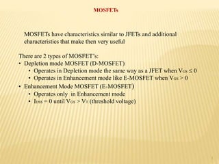
MOSFETs
MOSFETs have characteristics similar to JFETs and additional
characteristics that make then very useful
There are 2 types of MOSFET’s:
• Depletion mode MOSFET (D-MOSFET)
• Operates in Depletion mode the same way as a JFET when VGS 0
• Operates in Enhancement mode like E-MOSFET when VGS > 0
• Enhancement Mode MOSFET (E-MOSFET)
• Operates only in Enhancement mode
• IDSS = 0 until VGS > VT (threshold voltage)
2. BJT MOSFET
It is a current controlled device. It is a voltage controlled device.
It is a bipolar device (Current flows due
to both majority & minority carriers).
It is a unipolar device (Current flows
due to only majority carriers).
Thermal Runaway can damage the BJT Thermal Runaway does not take place
Input resistance (Ri) is very low. Output resistance (Ro) is very high.
Transfer characteristics are linear in
nature.
Transfer characteristics are non-linear in
nature.
BJT is More sensitive than MOSFET MOSFET is less Sensitive
AC Voltage Gain is HIGH AC Voltage Gain is Less
Bigger in size. Smaller in size.
Regions of operation: Saturation – ON
Switch , Cut off – OFF Switch
Active – Amplifier
Regions of operation: Ohmic – ON
Switch ,Saturation – Amplifier ,
Cut off – OFF Switch
It is more noisy. It is less noisy.
Switching speed is less. Switching speed is high.
Symbol Symbol
5 October 2023
2
3. THE MOSFET – DEPLETION MOSFET
Enhancement Mode With a
positive gate voltage, more
conduction electrons are attracted
into the channel, thus increasing
(enhancing) the channel
conductivity.
Depletion Mode With a negative gate voltage, the negative charges on the gate repel
conduction electrons from the channel, leaving positive ions in their place. Thereby, the n
channel is depleted of some of its electrons, thus decreasing the channel conductivity. The
greater the negative voltage on the gate, the greater the depletion of n-channel electrons. At
sufficiently negative gate-to-source voltage, VGS(off), the channel is totally depleted and
drain current is zero.
D-MOSFET schematic symbols.
Source
5. CONSTRUCTION OF N CHANNEL
DEPLETION TYPE MOSFET
• Two highly doped N regions are diffused into a lightly doped p type
substrate that may have an additional terminal connection called SS
• The two highly doped n regions represent source and drain connected via
an n-channel. The N-channel is formed by diffusion between the source
and drain. The type of impurity for the channel is the same as for the
source and drain.
• Metal is deposited through the holes to provide drain and source
terminals, and on the surface area between drain and source, a metal
plate is deposited. This layer constitutes the gate. The n-channel is
connected to the Gate (G) via a thin insulating layer of SiO2.
• The thin layer of SiO2 dielectric is grown over the entire surface and holes
are cut through the SiO2 (silicon-dioxide) layer to make contact with the N-
type blocks (Source and Drain).
6. OPERATION OF N CHANNEL
DEPLETION MOSFET
A D-MOSFET may be biased to operate in two modes:
the Depletion mode or the Enhancement mode
• When VGS =0 and drain is made positive with respect to source current(in the
form of free electrons) can flow between source and drain, even with zero
gate potential and the MOSFET is said to be operating in Enhancement
mode. In this mode of operation gate attracts the charge carriers from the P-
substrate to the N-channel and thus reduces the channel resistance which
increases the drain-current.
• When VGS = negative with respect to the substrate, the gate repels some of
the negative charge carriers out of the N-channel ,and attracts holes from the
p type substrate .This initiates recombination of holes and electrons. This
creates a depletion region in the channel and, therefore, reduces the number
of free electrons in the n channel, increases the channel resistance and
reduces the drain current. The more negative the gate, the less the drain
current. In this mode of operation the device is referred to as a depletion-
mode MOSFET. Here too much negative gate voltage can pinch-off the
channel.
• The more positive the gate is made, more number of electrons from p
substrate due to reverse leakage current and collisions between accelerating
particles the more drain current flows.
8. DRAIN CHARACTERISTICS
For VGS exceeding zero the device operates in
enhancement mode.
These drain curves again display an ohmic
region, a constant-current source region and a
cut-off region.
For a specified drain-source voltage VDS, VGS
(OFF) is the gate-source voltage at which drain
current reduces to a certain specified negligibly
small value,
For VGS between VGS (0FF) (-ve value)and zero,
the device operates in depletion-mode
9. 9
The transfer characteristics are similar
to the JFET
In Depletion Mode operation:
When VGS = 0V, ID = IDSS
When VGS < 0V, ID < IDSS
When VGS > 0V, ID > IDSS
Enhancement Mode operation
In this mode, the transistor operates with
VGS > 0V, and ID increases above IDSS
Shockley’s equation,
the formula used to plot the Transfer Curve
still applies but VGS is positive:
2
GS
D DSS
P
V
I = I 1-
V
11. 11
The p-channel Depletion mode MOSFET is similar to the n-channel except that
the voltage polarities and current directions are reversed
12. THE MOSFET – ENHANCEMENT MOSFET (E-MOSFET)
The schematic symbols for the n-channel
and p-channel E-MOSFET are shown in
Figure below.
The conventional enhancement MOSFETs
have a long thin lateral channel as shown
in structural view in Figure below.
Source
n
14. ENHANCEMENT MOSFET
CONSTRUCTION
Figure shows the construction of an N-channel E-MOSFET. The
main difference between the construction of DE-MOSFET and that of
E-MOSFET, the E-MOSFET substrate extends all the way to the
silicon dioxide (SiO2) and no channels are doped between the
source and the drain.
Two highly doped n regions are diffused into a lightly doped p
substrate that may have an additional terminal connection called SS
The source and drain are taken out through metallic contacts to n
doped regions. These n-doped regions are not connected via an n-
channel without an external voltage
The Gate (G) connects to the p-doped substrate via a thin insulating
layer of SiO2
Channels are electrically induced in these MOSFETs, when a
positive gate-source voltage VGS is applied to it.
15. N CHANNEL ENHANCEMENT
MOSFET OPERATION
• This MOSFET operates only in the enhancement mode and has no
depletion mode. It operates with large positive gate voltage only.
• When drain is applied with positive voltage with respect to source and
no potential is applied to the gate , a very small drain current that is,
reverse leakage current flows. The E MOSFET does not conduct when
the gate-source voltage VGS
= 0. This is the reason that it is called
normally-off MOSFET
• When the gate is made positive with respect to the source and the
substrate, negative (i.e. minority) charge carriers within the substrate
are attracted to the positive gate and accumulate close to the-surface of
the substrate. As the gate voltage is increased, more and more
electrons accumulate under the gate. Since these electrons can not
flow across the insulated layer of silicon dioxide to the gate, so they
accumulate at the surface of the substrate just below the gate. When
this occurs, a channel is induced by forming what is termed an
inversion layer (N-type). Now a drain current start flowing.
16. N CHANNEL ENHANCEMENT MOSFET
OPERATION
• At a particular value of VGS there is measurable current between drain and
source. This value of VGS is called threshold voltage VT. For any voltage below
VT, there is no channel
• The strength of the drain current depends upon the channel resistance which,
in turn, depends upon the number of charge carriers attracted to the positive
gate.
• Channel does not exist with VGS=0 and the conductivity of the channel is
enhanced by the positive bias on the gate so this device is also called the
enhancement MOSFET or E- MOSFET.
17. 17
Basic Operation
The Enhancement mode MOSFET only operates in the enhancement mode.
VGS is always positive
IDSS = 0 when VGS < VT
When VGS is greater than VT, the device turns- on and the drain current ID is controlled
by the gate voltage. As VGS increases above VT, the density of electrons in the induced
channel increases and ID increases. If VGS is kept constant and VDS is increased, then ID
saturates (IDSS)
The almost vertical components of the curves correspond to the ohmic region, and the
horizontal components correspond to the constant current region.
Thus E-MOSFET can be operated in either of these regions i.e. it can be used as a
variable-voltage resistor (WR) or as a constant current source.
18. 18
TRANSFER CHARACTERSTIC FOR
N CHANNEL ENHANCEMENT MOSFET
2
D GS T
I = k (V - V )
D(on)
2
GS(ON) T
I
k =
(V - V )
The current IDSS at VGS <=0 is very
small, When the VGS is made positive, the
drain current ID increases slowly at first,
and then much more rapidly with an
increase in VGS. The gate-source threshold
voltage VGST at which the drain current ID
attains some defined small value, say 10 u
A.
The equation for the transfer characteristic
of E-MOSFETs is given as:
19. E-MOSFET TRANSFER CHARACTERISTIC
CHARACTERISTICS AND PARAMETERS –
The E-MOSFET for all practical purposes does not conduct until VGS reaches the
threshold voltage (VGS(th)). ID when it is when conducting can be determined by the
formulas below. The constant K must first be determined. ID(on) is a data sheet given
value.
K = ID(on) /(VGS - VGS(th))2
ID = K(VGS - VGS(th))2
An n-channel device requires a
positive gate-to-source voltage, and
a p-channel device requires a
negative gate-to-source voltage.
E-MOSFET general transfer
characteristic curves.
33
20. 20
p-Channel Enhancement Mode MOSFETs
The p-channel Enhancement mode MOSFET is similar to the n-channel except
that the voltage polarities and current directions are reversed.