1. FET:-
FET stands for (Field Effect Transistor).
It has two types:
1: JFET
2: MOSFET
1-JFET
JFET stands for junction field effect transistor.
INTRODUTION:
JFET has the type of FET which is use for amplification of transistor .
It has voltage control device. It has depletion mode as 1: n-channel and 2: p-channel.
Construction:
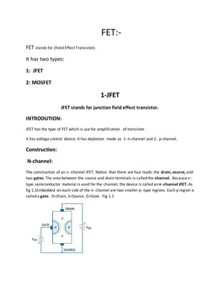
N-channel:
The construction of an n -channel JFET. Notice that there are four leads: the drain, source, and
two gates. The area between the source and drain terminals is called the channel. Because n -
type semiconductor material is used for the channel, the device is called an n -channel JFET. As
fig 1.1Embedded on each side of the n- channel are two smaller p- type regions. Each p region is
called a gate. D=Drain, S=Source, G=Gate. Fig 1.1
2. P-channel:
A p-channel JFET is shown in Fig c. Embedded on both sides of the p- channel are two n-
type gate regions. Again, these are normally connected together to form a single gate lead.
Reverse Bias of Gate :
In Fig. 1.2, the p-type gate and the n-type source
form the gate-source diode. With a JFET, we always reverse -bias the gate-source diode.
Because of reverse bias, the gate current IG is approximately zero, which is equivalent to saying
that the JFET has an almost infinite input resistance.
fig 1.2
Gate Voltage Controls Drain Current:
In Fig. 11-2, electrons flowing from the source to the drain must pass through the narrow
channel between the depletion layers.
When the gate voltage becomes more negative, the depletion layers expand and the
conducting channel becomes narrower. The more negative the gate voltage, the smaller the
current between the source and the drain. The JFET is a voltage-controlled device because an
input voltage controls an output current. In a JFET, the gate-to-source voltage VGS determines
3. How much current flows between the source and the drain . When VGS is zero, maximum
drain current flows through the JFET. This is why a JFET is referred to as a normally on device.
On the other hand, if VGS is negative enough, the depletion layers touch and the drain current
is cut off.
DRAIN Corves:
In Figure shows a JFET with normal biasing voltages. In this circuit, the
gate-source voltage VGS equals the gate supply voltage VGG, and the drain-source voltage VDS
equals the drain supply voltage VDD.
Maximum Drain Current:
If we short the gate to the source, as shown in Fig. we will
get maximum drain current because VGS 5 0. Figure shows the graph of drain current ID versus
drain-source voltage VDS for this shorted-gate condition. Notice how the drain current
increases rapidly and then becomes almost horizontal when VDS is greater than VP.
The active region of a JFET is between VP and VDS(max). The minimum voltage VP is called the
pinchoff voltage.
The ohmic region:
The almost-vertical part of the drain curve below pinchoff is called the
ohmic region.
Rds=Vp/Dss
4. 2-MOSFET:
MOSFET means (Metal Oxide Semiconductor Field effect Transistor).
Introduction:
MOSFET, has a source, gate, and drain. The MOSFET differs from the JFET,
however, in that the gate is insulated from the channel. Because of this, the gate current is
even smaller than it is in a JFET.
Types:
There are two kinds of MOSFETs, the depletion-mode type and the enhancement-
mode type. The enhancement-mode MOSFET is widely used in both discrete and integrated
circuits. In discrete circuits, the main use is in power switching, which means turning large
currents on and off . In integrated circuits, the main use is in digital switching, the basic process
behind modern computers. Although their use has declined, depletion mode MOSFETs are still
found in high-frequency front-end communications circuits as RF amplifiers.
The depletion mode MOSFET:
Depletion-mode MOSFET, a piece of n material with an insulated gate on the left and a p region
on the right. The p region is called the substrate. Electrons fl owing from source to drain must
pass through the narrow channel between the gate and the p substrate. A thin layer of silicon
dioxide (SiO2) is deposited on the left side of the channel. Silicon dioxide is the same as glass,
which is an insulator. In a MOSFET, the gate is metallic. Because the metallic gate is insulated
from the channel, negligible gate current fl ows even when the gate voltage is positive. Figure -
a shows a depletion-mode MOSFET with a negative gate voltage. The VDD supply forces free
electrons to fl ow from source to drain. These electrons fl ow through the narrow channel on
the left of the p substrate. As with a JFET, the gate voltage controls the width of the channel.
The more negative the gate voltage, the smaller the drain current. When the gate voltage is
negative enough, the drain current is cut off. Therefore, the operation of a depletion-mode
MOSFET is similar to that of a JFET when VGS is negative. Since the gate is insulated, we can
also use a positive input voltage, as shown in Fig. 12-2b. The positive gate voltage increases the
number of free electrons fl owing through the channel. The more positive the gate voltage, the
greater the conduction from source to drain.
5. D-MOSFET Curves:
Figure a shows the set of drain curves for a typical n-channel, depletion-mode MOSFET. Notice
that the curves above VGS = 0 are positive and the curves below VGS =0 are negative. As with a
JFET, the bottom curve is for VGS 5 VGS(off) and the drain current will be approximately zero.
As shown, when VGS = 0 V, the drain current will equal IDSS. This demonstrates that the
depletion-mode MOSFET, or D-MOSFET, is a normally on device. When VGS is made negative,
the drain current will be reduced. In contrast to an n-channel JFET, the n-channel D-MOSFET
can have VGS made positive and still function properly. This is because there is no p-n junction
to become forward biased. When VGS becomes positive, ID will increase following the square-
law equation: ID = IDSS ( 1 * VGS /VGS(off) ) 2
6. SYMBEL:
a)n-channel b)p-channel.
Depletion-Mode MOSFET Amplifiers:
A depletion-mode MOSFET is unique because it can operate with a positive or a negative gate
voltage. Because of this, we can set its Q point at VGS = 0 V.
When the input signal goes positive, it increases ID above IDSS. When the input signal goes
negative, it decreases ID below IDSS. Because there is no pn junction to forward bias, the input
resistance of the MOSFET r emains very high. Being able to use zero VGS allows us to build the
very simple bias circuit .
Because IG is zero, VGS 5 0 V and ID 5 IDSS. The drain voltage is: VDS =Vdd * IDss Rd .Due to
the fact that a D-MOSFET is a normally on device.
it is also possible to use self-bias by adding a source resistor. The operation becomes the same
as a self-biased JFET circuit.
The Enhancement-Mode MOSFET :
The depletion-mode MOSFET was part of the evolution toward the enhancement- mode
MOSFET, abbreviated E-MOSFET. Without the E-MOSFET, the personal computers that are now
so widespread would not exist.
7. BJT
BJT means (Bipolar Junction Transistor).
Introduction:
Transistors are used when it is necessary to amplify voltage, current, and power. With a small
signal applied to the transistor amplifier, the transistor and its associated circuitry can produce
an amplified version of the input signal. The output signal can be hundreds or even thousands
of times larger than the input signal. In computer circuits, the transistor can be used as an
electronic switch.
TransistorConstruction : A transistor has three doped regions, as shown in Figure
a shows an npn transistor, and Fig. b shows a pnp transistor. Notice that for both types, the
base is a narrow region sandwiched between the larger collector and emitter regions. The
emitter region of a transistor is heavily doped. Its job is to emit or inject current carriers into
the base. The base region is very thin and lightly doped. Most of the current carriers injected
into the base from the emitter do not flow out the base lead. Instead, most of the current
carriers injected into the base pass on to the collector. The collector region is moderately
doped and is the largest of all three regions. The collector region attracts the current carriers
that are injected into the thin and lightly doped base region. Incidentally, the collector region is
the largest of all three regions because it must dissipate more heat than the emitter or base
regions. In npn transistors, the majority current carriers are free electrons in the emitter
and collector, whereas the majority current carriers are holes in the base. The opposite is true
in a pnp transistor where the majority current carriers are holes in the emitter and collector,
and the majority current carriers are free electrons in the base.
a.
8. b
Proper Transistor Biasing:
For a transistor to function properly as an amplifi er, the
emitter-base junction must be forward-biased, and the collector-base junction must be reverse-
biased, as illustrated in Fig. a. Notice the common connection for the voltage sources at the
base lead of the transistor. The emitter-base supply voltage is designated V EE and the
collector-base supply voltage is designated Vcc .
Transistor Currents :
Figure b shows the emitter current, IE , the base current, IB ,
and the collector current, IC . Electrons in the n -type emitter are repelled into the base by the
negative terminal of the emitter supply voltage, VEE. Since the base is very thin and lightly
doped, only a few electrons combine with holes in the base. The small current flowing out of
the base lead (which is the base current, IB) is called recombination current because free
electrons injected into the base must fall into a hole before they can flow out the base lead.
Notice in Fig. b that most of the emitter-injected electrons pass through the base region and
into the collector region. The reason is two fold. First, only a few holes are available for
recombination in the base. Second, the positive collector-base voltage attracts the free
electrons in the p-type base over to the collector side before they can recombine with holes in
the base. In most transistors, the collector current, IC, is nearly identical to the emitter
current, IE. This is equivalent to saying that the recombination current, IB , is very small. Only
a small voltage is needed to create an electric field strong enough in the collector -base
junction to collect almost all free electrons injected into the base. After the collector-base
voltage reaches a certain level, increasing it further will have little or no effect on the number
9. of free electrons entering the collector. As a matter of fact, after the collector-base voltage is
slightly above zero, full current is obtained
DC Alpha:
A characteristic that describes how closely the emitter and collector currents are
in a common base circuit is called the dc alpha. This is expressed in Formula .
Adc= IC/ IE.
DC Beta:
The dc current gain of a transistor in the common-emitter connection is called the
dc beta. The dc beta is expressed in Formula .
Bdc=IcIb.