Downloaded 64 times
![14
What is an HDL? (continued)
module counter(clk,rst_n,cnt);
input clk,rst_n;
output [3:0] cnt;
reg [3:0] cnt;
always @(posedge clk) begin
if (~rst_n)
cnt = 4’b0000;
else
cnt = cnt+1;
end
endmodule
• It looks like a programming language
• It is NOT a programming language
It is always critical to recall you
are describing hardware
This codes primary purpose is to
generate hardware
The hardware this code describes
(a counter) can be simulated on a
computer. In this secondary use of
the language it does act more like a
programming language.](https://image.slidesharecdn.com/lecture1-150105073355-conversion-gate02/75/Verilog-Lecture1-14-2048.jpg)
![16
What is Synthesis?
Takes a description of what a circuit DOES
Creates the hardware to DO it
module counter(clk,rst_n,cnt);
input clk,rst_n;
output [3:0] cnt;
reg [3:0] cnt;
always @(posedge clk) begin
if (~rst_n)
cnt = 4’b0000;
else
cnt = cnt+1;
end
endmodule
SynthesisTool
(Synopsys)
Increment
Combinational
Logic
rst_n 44 4
clk
cnt[3:0]
Output is actually a text
netlist, not a GUI schematic
form.](https://image.slidesharecdn.com/lecture1-150105073355-conversion-gate02/75/Verilog-Lecture1-16-2048.jpg)
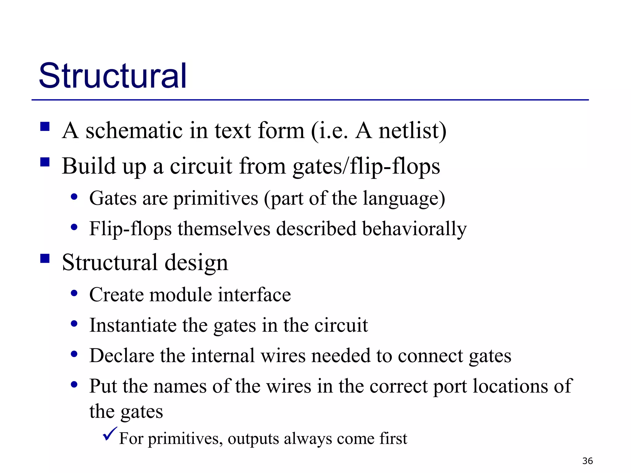
![31
Verilog Module
In Verilog, a circuit is a module.
module decoder_2_to_4 (A, D) ;
input [1:0] A ;
output [3:0] D ;
assign D = (A == 2'b00) ? 4'b0001 :
(A == 2'b01) ? 4'b0010 :
(A == 2'b10) ? 4'b0100 :
(A == 2'b11) ? 4'b1000 ;
endmodule
Decoder
2-to-4
A[1:0]
D[3:0]
2
4](https://image.slidesharecdn.com/lecture1-150105073355-conversion-gate02/75/Verilog-Lecture1-31-2048.jpg)
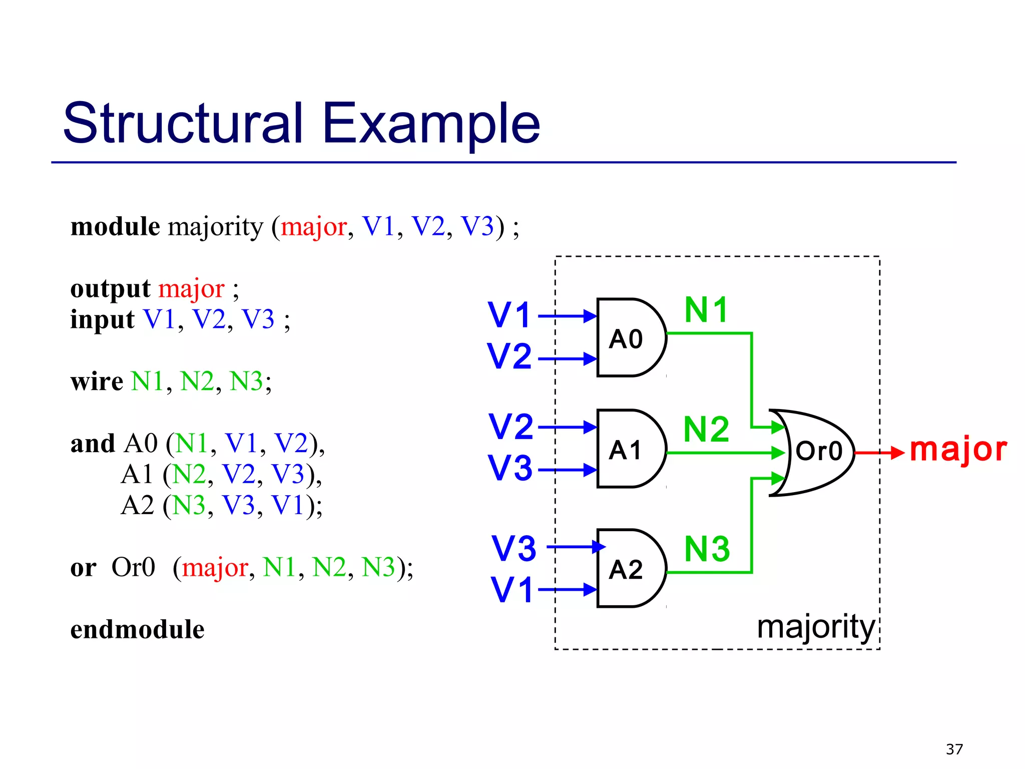
![32
Verilog Module
module decoder_2_to_4 (A, D) ;
input [1:0] A ;
output [3:0] D ;
assign D = (A == 2'b00) ? 4'b0001 :
(A == 2'b01) ? 4'b0010 :
(A == 2'b10) ? 4'b0100 :
(A == 2'b11) ? 4'b1000 ;
endmodule
Decoder
2-to-4
A[1:0]
D[3:0]
2
4
ports names
of module
module name
port
types
port
sizes
module
contents
keywords underlined](https://image.slidesharecdn.com/lecture1-150105073355-conversion-gate02/75/Verilog-Lecture1-32-2048.jpg)
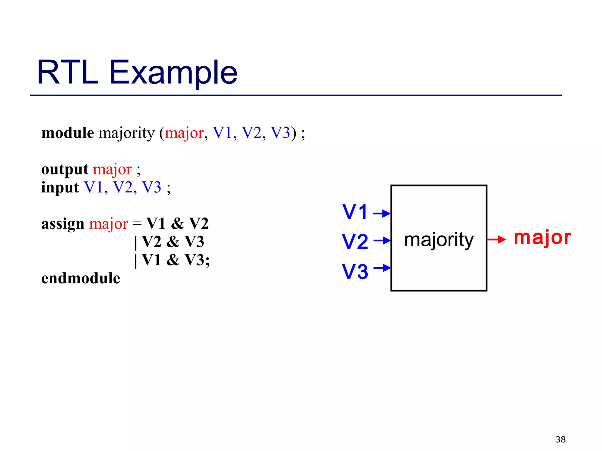
![34
Declaring Ports
A signal is attached to every port
Declare type of port
• input
• output
• inout (bidirectional)
Scalar (single bit) - don’t specify a size
• input cin;
Vector (multiple bits) - specify size using range
• Range is MSB to LSB (left to right)
• Don’t have to include zero if you don’t want to… (D[2:1])
• output [7:0] OUT;
• input [0:4] IN;](https://image.slidesharecdn.com/lecture1-150105073355-conversion-gate02/75/Verilog-Lecture1-34-2048.jpg)

This document provides an overview of the ECE 551 Digital Design and Synthesis course for Fall 2009 at UW-Madison. It introduces the instructor, Eric Hoffman, and TA Vinod Nalamalapu. It outlines course goals, materials, tools, evaluation criteria and schedule. Key topics covered include Verilog, simulation, synthesis, FPGAs, standard cells and digital design flows. Students are expected to have prior knowledge of digital logic concepts from ECE 352.