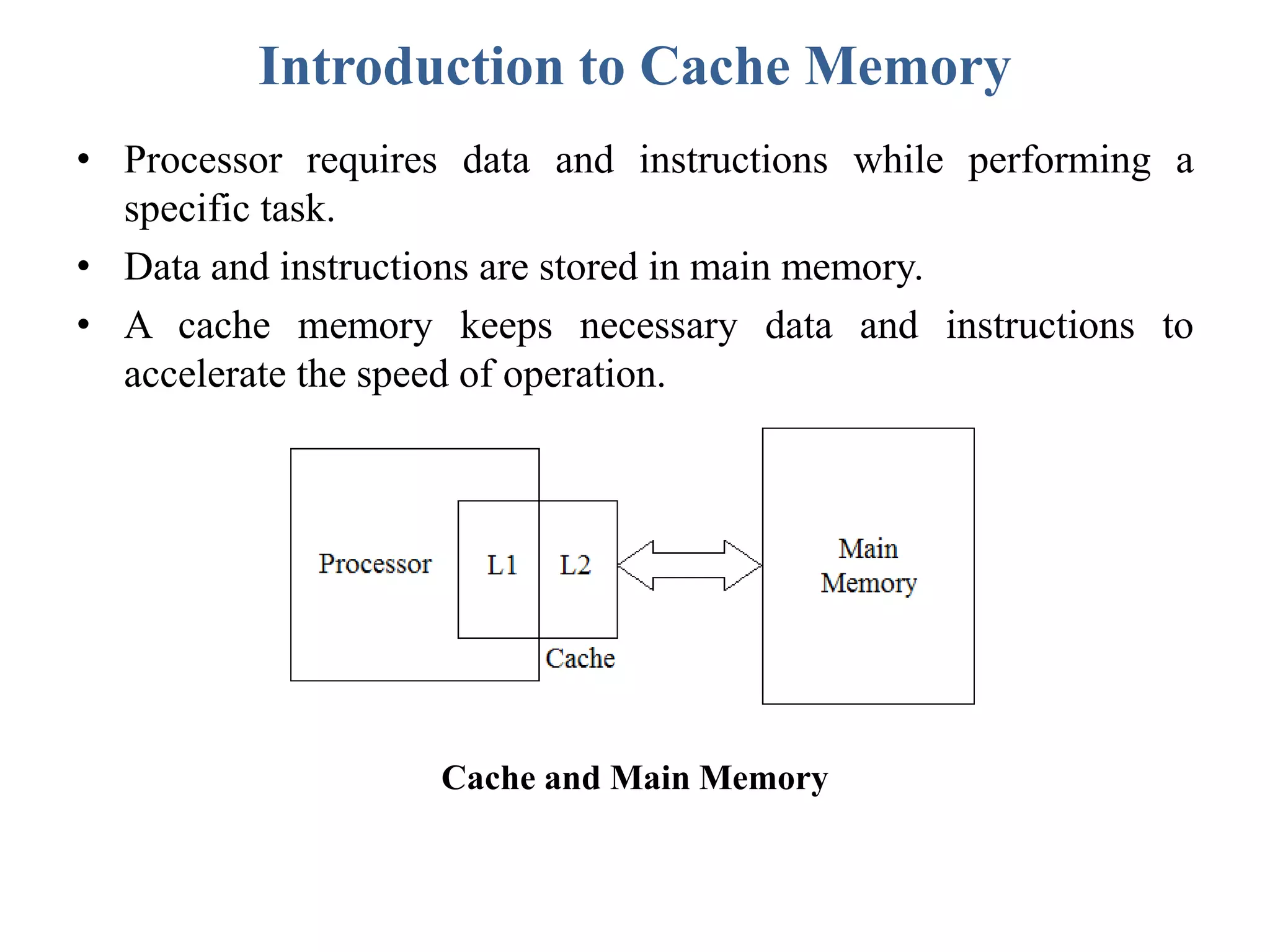
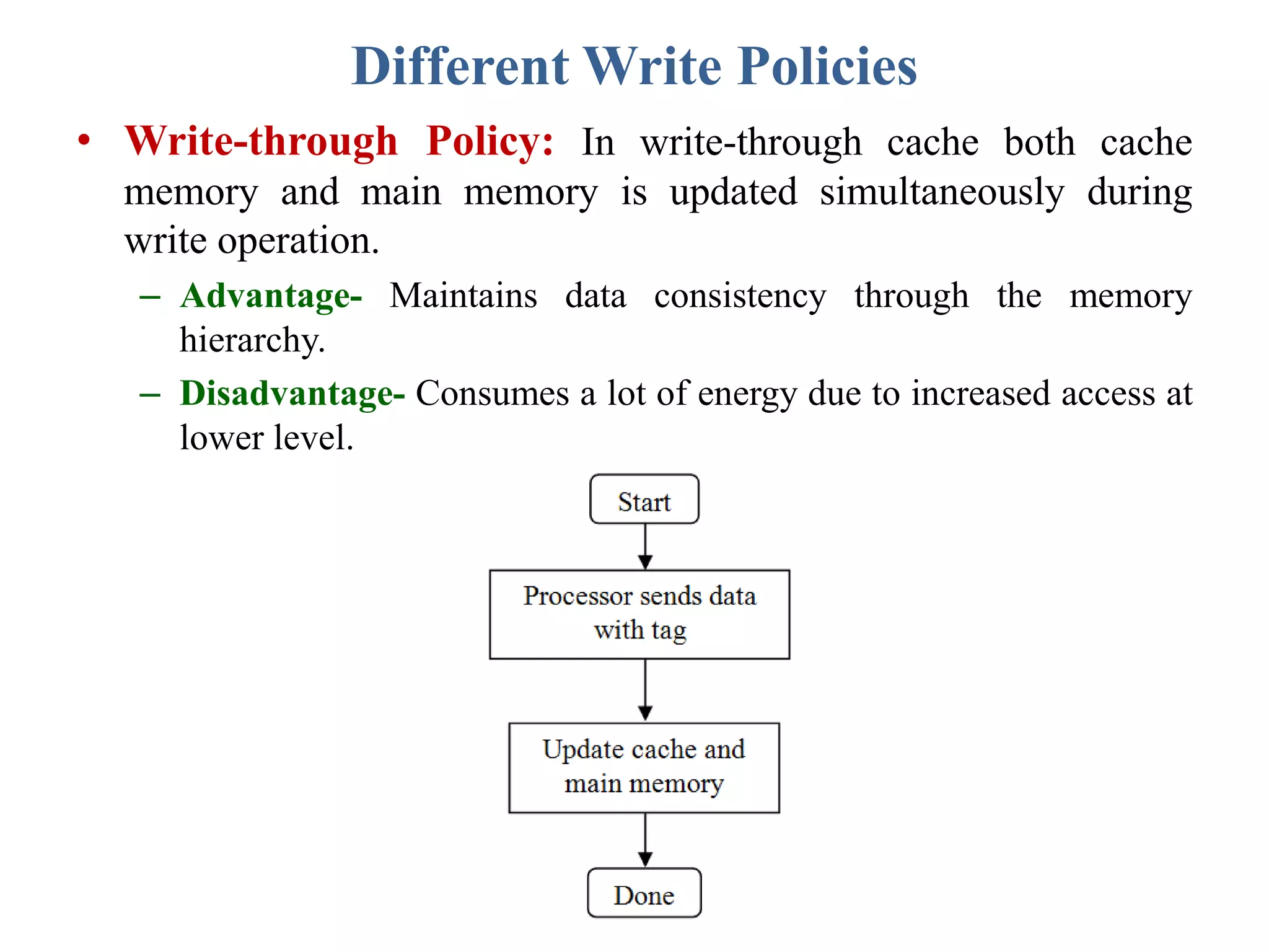
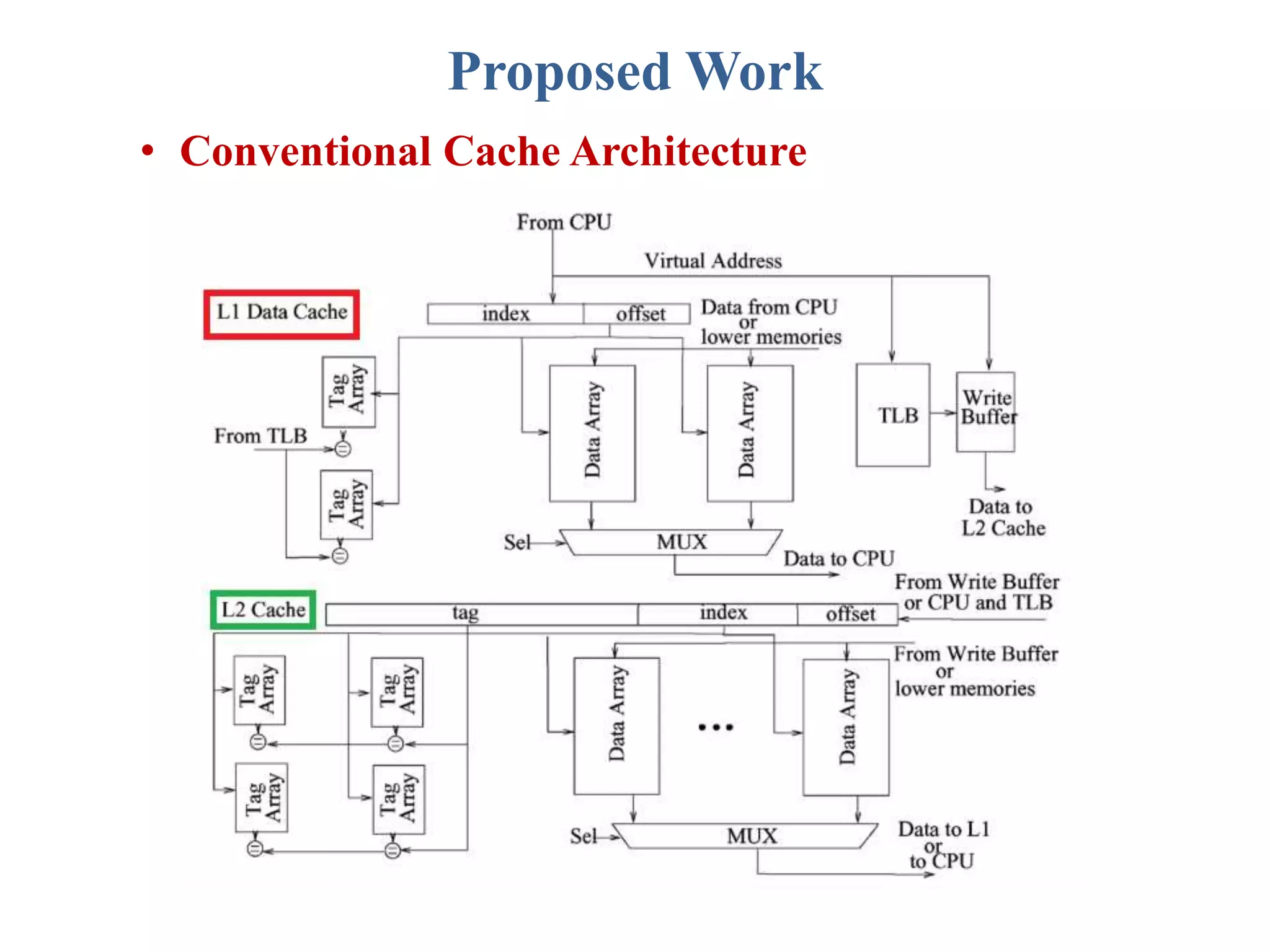
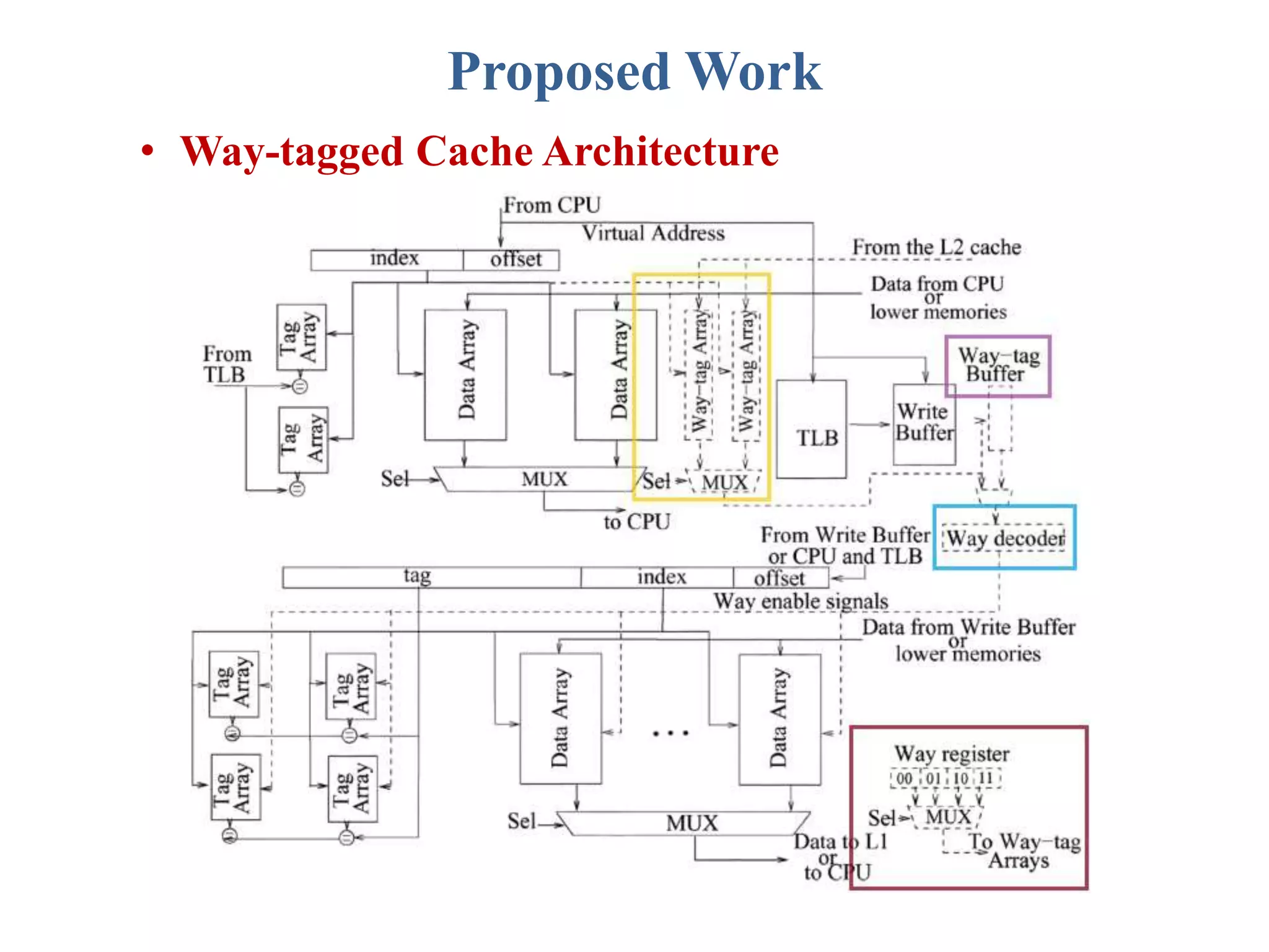
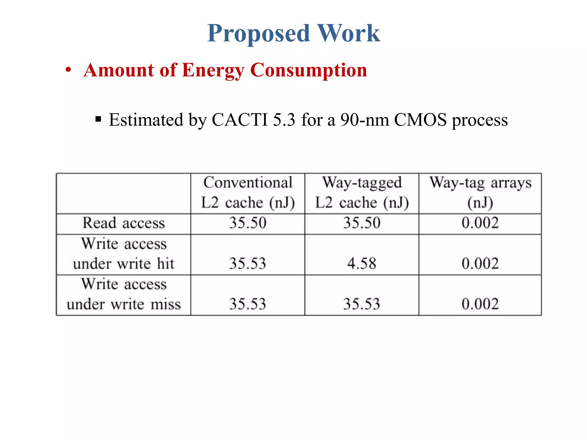
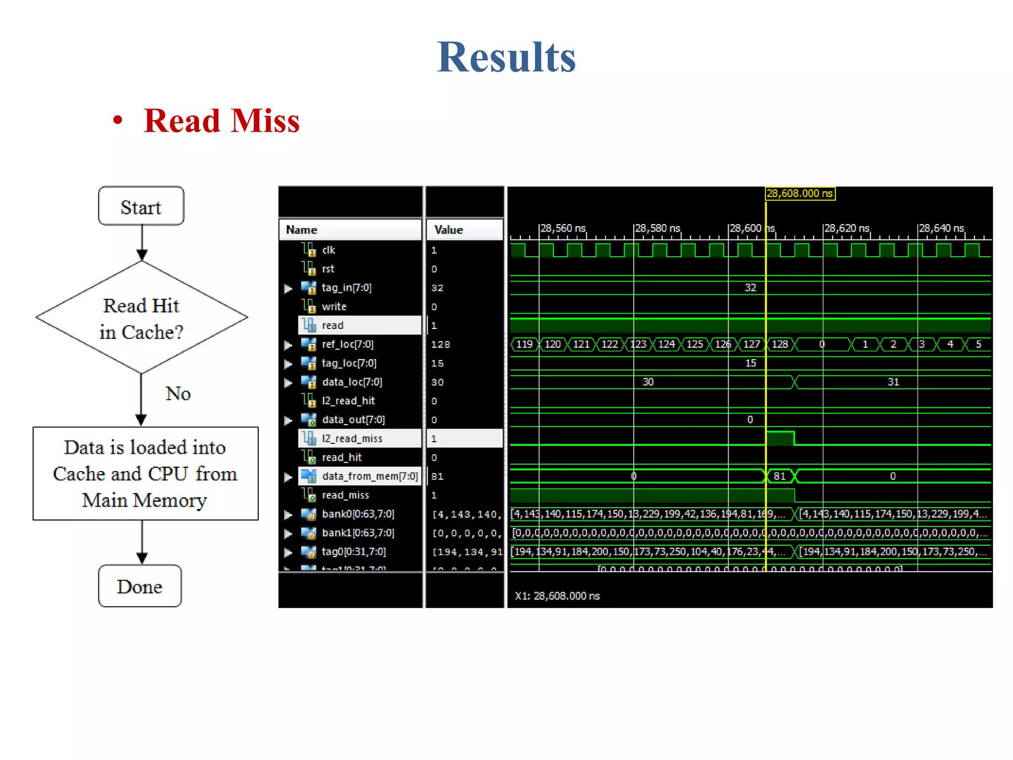
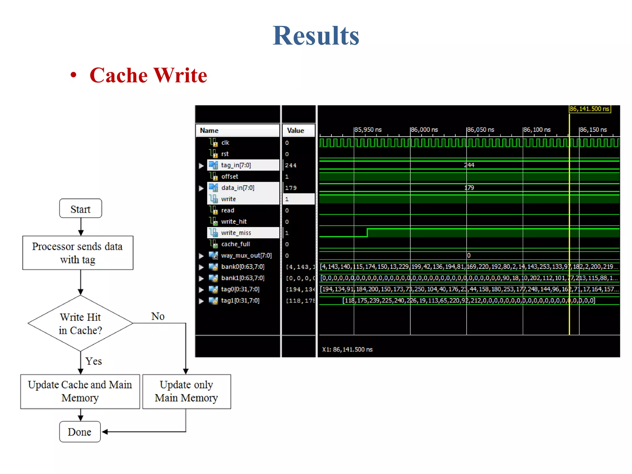
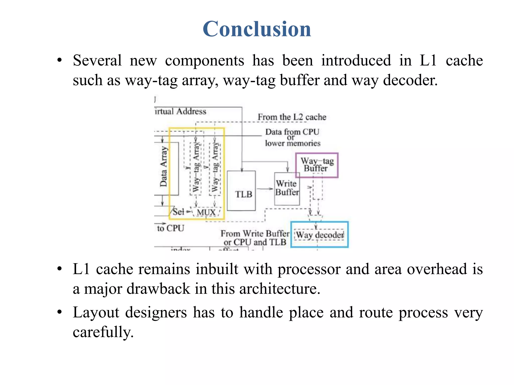
This document describes a student's project to design an energy efficient cache memory using Verilog HDL. It presents the background and motivation, including that write-through caches consume a lot of energy due to increased access at lower levels. The proposed work introduces a way-tagged cache architecture to reduce energy consumption. Simulation results show energy savings of the proposed cache compared to a conventional cache for various operations like reset, data load, read and write hits/misses. The conclusion is that the way-tagged cache adds new components to L1 cache but remains inbuilt with the processor, with area overhead as a drawback.
![References
• [1]. An Energy-Efficient L2 Cache Architecture Using Way Tag Information Under Write-Through Policy,
Jianwei Dai and Lei Wang, Senior Member, IEEE, IEEE Transactions on Very Large Scale Integration
(VLSI) Systems, Vol. 21, No. 1, January 2013
• [2]. G. Konstadinidis, K. Normoyle, S. Wong, S. Bhutani, H. Stuimer, T. Johnson, A. Smith, D. Cheung, F.
Romano, S. Yu, S. Oh, V.Melamed, S. Narayanan, D. Bunsey, C. Khieu, K. J. Wu, R. Schmitt, A. Dumlao,
M. Sutera, J. Chau, andK. J. Lin, “Implementation of a third-generation 1.1-GHz 64-bit microprocessor,”
IEEE J. Solid-State Circuits, vol. 37, no. 11, pp. 1461–1469, Nov. 2002.
• [3]. S. Rusu, J. Stinson, S. Tam, J. Leung, H. Muljono, and B. Cherkauer, “A 1.5-GHz 130-nm itanium 2
processor with 6-MB on-die L3 cache,” IEEE J. Solid-State Circuits, vol. 38, no. 11, pp. 1887–1895, Nov.
2003.
• [4]. D. Wendell, J. Lin, P. Kaushik, S. Seshadri, A. Wang, V. Sundararaman, P. Wang, H. McIntyre, S. Kim,
W. Hsu, H. Park, G. Levinsky, J. Lu, M. Chirania, R. Heald, and P. Lazar, “A 4 MB on-chip L2 cache for a
90 nm 1.6 GHz 64 bit SPARC microprocessor,” in IEEE Int. Solid-State Circuits Conf. (ISSCC) Dig. Tech.
Papers, 2004, pp. 66–67.
• [5]. http://en.wikipedia.org/wiki/CPU_cache
• [6]. C. Su and A. Despain, “Cache design tradeoffs for power and performance optimization: A case study,”
in Proc. Int. Symp. Low Power Electron. Design, 1997, pp. 63–68.
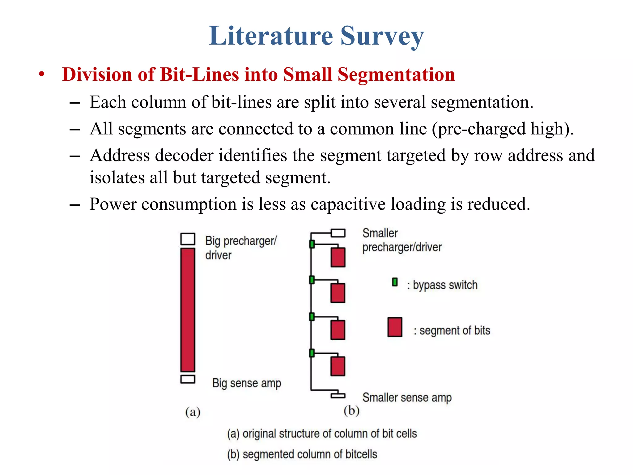
• [7]. K. Ghose and M. B.Kamble, “Reducing power in superscalar processor caches using subbanking,
multiple line buffers and bit-line segmentation,” in Proc. Int. Symp. Low Power Electron. Design, 1999, pp.
70–75.
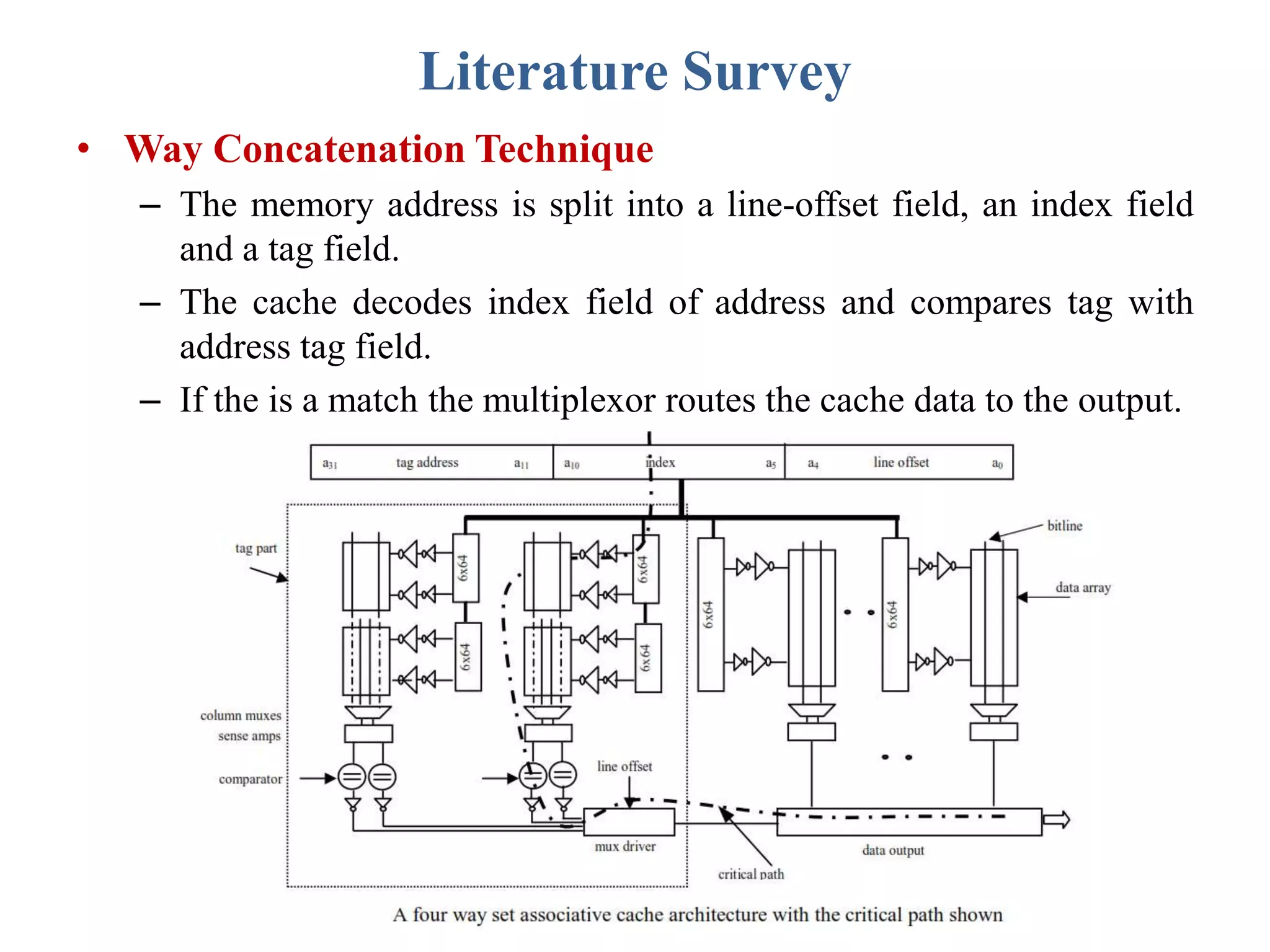
• [8]. C. Zhang, F. Vahid, and W. Najjar, “A highly-configurable cache architecture for embedded systems,”
in Proc. Int. Symp. Comput. Arch., 2003, pp. 136–146.
• [9]. K. Inoue, T. Ishihara, and K. Murakami, “Way-predicting set-associative cache for high performance
and low energy consumption,” in Proc. Int. Symp. Low Power Electron. Design, 1999, pp. 273–275.
• [10]. A.Ma, M. Zhang, and K.Asanovi, “Way memoization to reduce fetch energy in instruction caches,” in
Proc. ISCA Workshop Complexity Effective Design, 2001, pp. 1–9.
• [11]. T. Ishihara and F. Fallah, “A way memorization technique for reducing power consumption of caches
in application specific integrated processors,” in Proc. Design Autom. Test Euro. Conf., 2005, pp. 358–363.
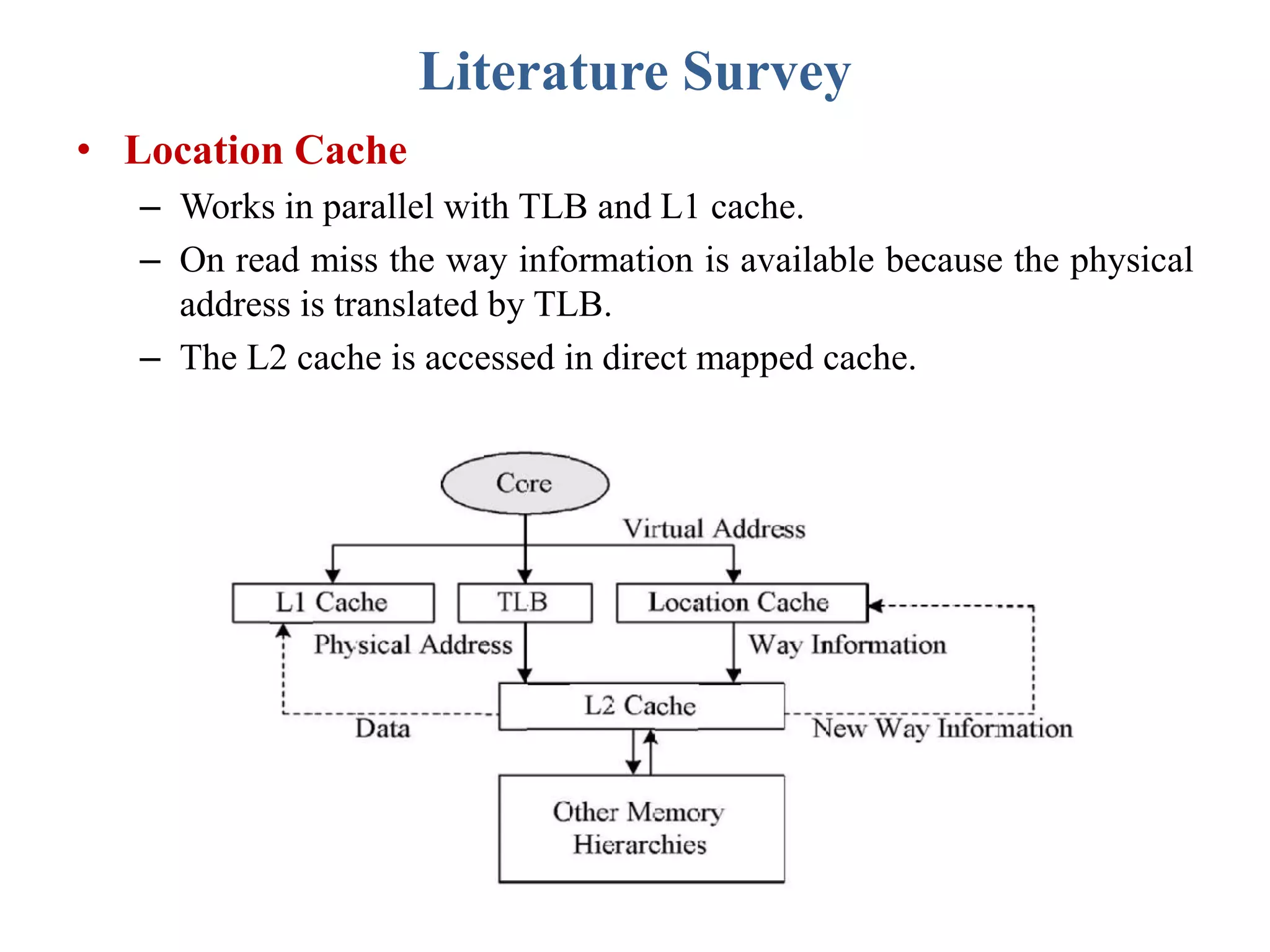
• [12]. R. Min, W. Jone, and Y. Hu, “Location cache: A low-power L2 cache system,” in Proc. Int. Symp.
Low Power Electron. Design, 2004, pp. 120–125.](https://image.slidesharecdn.com/e9873924-942b-4da3-873b-d877eff6458f-151111164735-lva1-app6891/75/Project-Presentation-Final-31-2048.jpg)