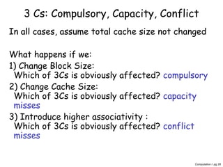
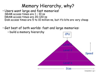
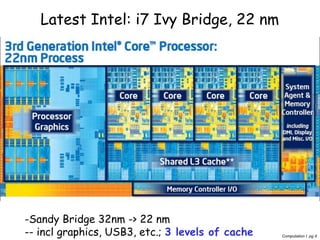
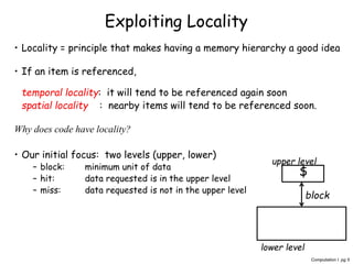
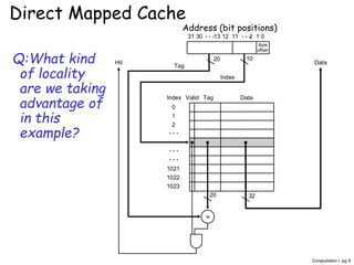
Computation I pg 1
Memory Hierarchy, why?
• Users want large and fast memories!
SRAM access times are 1 – 10 ns
DRAM access times are 20-120 ns
Disk access times are 5 to 10 million ns, but it’s bits are very cheap
• Get best of both worlds: fast and large memories:
– build a memory hierarchy
CPU
Level 1
Level 2
Level n
Size
Speed
Computation I pg 2
Memory recap
• We can build a memory – a logical k × m array of
stored bits. Usually m = 8 bits / location
•
•
•
n bits address
k = 2n locations
m bits data / entry
Address Space:
number of locations
(usually a power of 2)
Addressability:
m: number of bits per location
(e.g., byte-addressable)
Computation I pg 3
• SRAM:
– value is stored with a pair of inverting gates
– very fast but takes up more space than DRAM (4 to 6
transistors)
• DRAM:
– value is stored as a charge on capacitor (must be
refreshed)
– very small but slower than SRAM (factor of 5 to 10)
– charge leakes =>
• refresh needed
Memory element: SRAM vs DRAM
Word line
Pass transistor
Capacitor
Bit line
Computation I pg 4
Latest Intel: i7 Ivy Bridge, 22 nm
-Sandy Bridge 32nm -> 22 nm
-- incl graphics, USB3, etc.; 3 levels of cache
Computation I pg 5
Exploiting Locality
• Locality = principle that makes having a memory hierarchy a good idea
• If an item is referenced,
temporal locality: it will tend to be referenced again soon
spatial locality : nearby items will tend to be referenced soon.
Why does code have locality?
• Our initial focus: two levels (upper, lower)
– block: minimum unit of data
– hit: data requested is in the upper level
– miss: data requested is not in the upper level
block
$
lower level
upper level
Computation I pg 6
Cache operation
Memory/Lowerlevel
Cache / Higher level
block / line
tags data
Computation I pg 7
• Mapping: cache address is memory address modulo the
number of blocks in the cache
Direct Mapped Cache
00001 00101 01001 01101 10001 10101 11001 11101
000
Cache
Memory
001
010
011
100
101
110
111
Computation I pg 8
Q:What kind
of locality
are we taking
advantage of
in this
example?
Direct Mapped Cache
20 10
Byte
offset
Valid Tag DataIndex
0
1
2
1021
1022
1023
Tag
Index
Hit Data
20 32
31 30 13 12 11 2 1 0
Address (bit positions)
Computation I pg 9
• This example exploits (also) spatial locality (having
larger blocks):
Direct Mapped Cache
Address (showing bit positions)
16 12 Byte
offset
V Tag Data
Hit Data
16 32
4K
entries
16 bits 128 bits
Mux
32 32 32
2
32
Block offsetIndex
Tag
31 16 15 4 32 1 0
Address (bit positions)
Computation I pg 10
• Read hits
– this is what we want!
• Read misses
– stall the CPU, fetch block from memory, deliver to cache, restart the
load instruction
• Write hits:
– can replace data in cache and memory (write-through)
– write the data only into the cache (write-back the cache later)
• Write misses:
– read the entire block into the cache, then write the word (allocate on
write miss)
– do not read the cache line; just write to memory (no allocate on write
miss)
Hits vs. Misses
Computation I pg 11
Splitting first level cache
• Use split Instruction and Data caches
– Caches can be tuned differently
– Avoids dual ported cache
Program
Block size in
words
Instruction
miss rate
Data miss
rate
Effective combined
miss rate
gcc 1 6.1% 2.1% 5.4%
4 2.0% 1.7% 1.9%
spice 1 1.2% 1.3% 1.2%
4 0.3% 0.6% 0.4%
CPU
I$
D$
I&D
$
Main Memory
L1 L2
Computation I pg 12
Let’s look at cache&memory performance
Texec = Ncycles • Tcycle = Ninst• CPI • Tcycle
with
CPI = CPIideal + CPIstall
CPIstall = %reads • missrateread • misspenaltyread+
%writes • missratewrite • misspenaltywrite
or:
Texec = (Nnormal-cycles + Nstall-cycles ) • Tcycle
with
Nstall-cycles = Nreads • missrateread • misspenaltyread +
Nwrites • missratewrite • misspenaltywrite
(+ Write-buffer stalls )
Computation I pg 13
Performance example (1)
• Assume application with:
– Icache missrate 2%
– Dcache missrate 4%
– Fraction of ld-st instructions = 36%
– CPI ideal (i.e. without cache misses) is 2.0
– Misspenalty 40 cycles
• Calculate CPI taking misses into account
CPI = 2.0 + CPIstall
CPIstall = Instruction-miss cycles + Data-miss cycles
Instruction-miss cycles = Ninstr x 0.02 x 40 = 0.80 Ninstr
Data-miss cycles = Ninstr x %ld-st x 0.04 x 40
CPI = 3.36
Slowdown: 1.68 !!
Computation I pg 14
Performance example (2)
1. What if ideal processor had CPI = 1.0 (instead of 2.0)
• Slowdown would be 2.36 !
2. What if processor is clocked twice as fast
• => penalty becomes 80 cycles
• CPI = 4.75
• Speedup = N.CPIa.Tclock / (N.CPIb.Tclock/2) =
3.36 / (4.75/2)
• Speedup is not 2, but only 1.41 !!
Computation I pg 15
Improving cache / memory performance
• Ways of improving performance:
– decreasing the miss ratio (avoiding conflicts): associativity
– decreasing the miss penalty: multilevel caches
– Adapting block size: see earlier slides
– Note: there are many more ways to improve memory
performance
(see e.g. master course 5MD00)
Computation I pg 16
How to reduce CPIstall ?
CPIstall = %reads • missrateread • misspenaltyread+
%writes • missratewrite • misspenaltywrite
Reduce missrate:
• Larger cache
– Avoids capacity misses
– However: a large cache may increase Tcycle
• Larger block (line) size
– Exploits spatial locality: see previous lecture
• Associative cache
– Avoids conflict misses
Reduce misspenalty:
• Add 2nd level of cache
Computation I pg 17
Decreasing miss ratio with
associativity
Tag Data Tag Data Tag Data Tag Data Tag Data Tag Data Tag Data Tag Data
Eight-way set associative (fully associative)
Tag Data Tag Data Tag Data Tag Data
Four-way set associative
Set
0
1
Tag Data
One-way set associative
(direct mapped)
Block
0
7
1
2
3
4
5
6
Tag Data
Two-way set associative
Set
0
1
2
3
Tag Data
block
2 blocks / set
4 blocks / set
8 blocks / set
Computation I pg 18
An implementation: 4 way associative
Address
22 8
V TagIndex
0
1
2
253
254
255
Data V Tag Data V Tag Data V Tag Data
3222
4-to-1 multiplexor
Hit Data
123891011123031 0
Computation I pg 19
Performance of Associative Caches
0%
3%
6%
9%
12%
15%
Eight-wayFour-wayTwo-wayOne-way
1 KB
2 KB
4 KB
8 KB
Missrate
Associativity 16 KB
32 KB
64 KB
128 KB
1 KB
2 KB
8 KB
Computation I pg 20
Further Cache Basics
•cache_size = Nsets x Associativity x Block_size
•block_address = Byte_address DIV Block_size in
bytes
•index size = Block_address MOD Nsets
• Because the block size and the number of sets are
(usually) powers of two, DIV and MOD can be performed
efficiently
tag index block
offset
block address
… 2 1 0bit 31 …
Computation I pg 21
Comparing different (1-level) caches (1)
• Assume
– Cache of 4K blocks
– 4 word block size
– 32 bit address
• Direct mapped (associativity=1) :
– 16 bytes per block = 2^4
– 32 bit address : 32-4=28 bits for index and tag
– #sets=#blocks/ associativity : log2 of 4K=12 : 12 for index
– Total number of tag bits : (28-12)*4K=64 Kbits
• 2-way associative
– #sets=#blocks/associativity : 2K sets
– 1 bit less for indexing, 1 bit more for tag
– Tag bits : (28-11) * 2 * 2K=68 Kbits
• 4-way associative
– #sets=#blocks/associativity : 1K sets
– 1 bit less for indexing, 1 bit more for tag
– Tag bits : (28-10) * 4 * 1K=72 Kbits
Computation I pg 22
Comparing different (1-level) caches (2)
3 caches consisting of 4 one-word blocks:
• Cache 1 : fully associative
• Cache 2 : two-way set associative
• Cache 3 : direct mapped
Suppose following sequence of block
addresses: 0, 8, 0, 6, 8
Computation I pg 23
Direct Mapped
Block address Cache Block
0 0 mod 4=0
6 6 mod 4=2
8 8 mod 4=0
Address of
memory block
Hit or
miss
Location
0
Location
1
Location
2
Location
3
0 miss Mem[0]
8 miss Mem[8]
0 miss Mem[0]
6 miss Mem[0] Mem[6]
8 miss Mem[8] Mem[6]
Coloured = new entry = miss
Computation I pg 24
2-way Set Associative:
2 sets
Block address Cache Block
0 0 mod 2=0
6 6 mod 2=0
8 8 mod 2=0
Address of
memory block
Hit or
miss
SET 0
entry 0
SET 0
entry 1
SET 1
entry 0
SET 1
entry 1
0 Miss Mem[0]
8 Miss Mem[0] Mem[8]
0 Hit Mem[0] Mem[8]
6 Miss Mem[0] Mem[6]
8 Miss Mem[8] Mem[6]
LEAST RECENTLY USED BLOCK
(so all in set/location 0)
Computation I pg 25
Fully associative
(4 way assoc., 1 set)
Address of
memory block
Hit or
miss
Block 0 Block 1 Block 2 Block 3
0 Miss Mem[0]
8 Miss Mem[0] Mem[8]
0 Hit Mem[0] Mem[8]
6 Miss Mem[0] Mem[8] Mem[6]
8 Hit Mem[0] Mem[8] Mem[6]
Computation I pg 26
Review: Four Questions for Memory
Hierarchy Designers
•Q1: Where can a block be placed in the upper
level? (Block placement)
– Fully Associative, Set Associative, Direct Mapped
•Q2: How is a block found if it is in the upper
level?
(Block identification)
– Tag/Block
•Q3: Which block should be replaced on a miss?
(Block replacement)
– Random, FIFO, LRU
•Q4: What happens on a write?
(Write strategy)
– Write Back or Write Through (with Write Buffer)
Computation I pg 27
Classifying Misses: the 3 Cs
•The 3 Cs:
– Compulsory—First access to a block is always a
miss. Also called cold start misses
• misses in infinite cache
– Capacity—Misses resulting from the finite
capacity of the cache
• misses in fully associative cache with optimal replacement strategy
– Conflict—Misses occurring because several blocks
map to the same set. Also called collision misses
• remaining misses
Computation I pg 28
3 Cs: Compulsory, Capacity, Conflict
In all cases, assume total cache size not changed
What happens if we:
1) Change Block Size:
Which of 3Cs is obviously affected? compulsory
2) Change Cache Size:
Which of 3Cs is obviously affected? capacity
misses
3) Introduce higher associativity :
Which of 3Cs is obviously affected? conflict
misses
Computation I pg 29
Cache Size (KB)
MissRateperType
0
0.02
0.04
0.06
0.08
0.1
0.12
0.14
1
2
4
8
16
32
64
128
1-way
2-way
4-way
8-way
Capacity
Compulsory
3Cs Absolute Miss Rate (SPEC92)
Conflict
Miss rate per type
Computation I pg 30
Second Level Cache (L2)
• Most CPUs
– have an L1 cache small enough to match the cycle time
(reduce the time to hit the cache)
– have an L2 cache large enough and with sufficient
associativity to capture most memory accesses (reduce
miss rate)
• L2 Equations, Average Memory Access Time (AMAT):
AMAT = Hit TimeL1 + Miss RateL1 x Miss PenaltyL1
Miss PenaltyL1 = Hit TimeL2 + Miss RateL2 x Miss PenaltyL2
AMAT = Hit TimeL1 + Miss RateL1 x (Hit TimeL2 + Miss RateL2 x Miss
PenaltyL2)
• Definitions:
– Local miss rate— misses in this cache divided by the total number
of memory accesses to this cache (Miss rateL2)
– Global miss rate—misses in this cache divided by the total number
of memory accesses generated by the CPU
(Miss RateL1 x Miss RateL2)
Computation I pg 31
Second Level Cache (L2)
• Suppose processor with base CPI of 1.0
• Clock rate of 500 Mhz
• Main memory access time : 200 ns
• Miss rate per instruction primary cache : 5%
What improvement with second cache having 20ns access time,
reducing miss rate to memory to 2% ?
• Miss penalty : 200 ns/ 2ns per cycle=100 clock cycles
• Effective CPI=base CPI+ memory stall per instruction = ?
– 1 level cache : total CPI=1+5%*100=6
– 2 level cache : a miss in first level cache is satisfied by second cache or
memory
• Access second level cache : 20 ns / 2ns per cycle=10 clock cycles
• If miss in second cache, then access memory : in 2% of the cases
• Total CPI=1+primary stalls per instruction +secondary stalls per instruction
• Total CPI=1+5%*10+2%*100=3.5
Machine with L2 cache : 6/3.5=1.7 times faster
Computation I pg 32
Second Level Cache
• Global cache miss is similar to single cache miss rate of second
level cache provided L2 cache is much bigger than L1.
• Local cache rate is NOT good measure of secondary caches as it is function
of L1 cache.
Global cache miss rate should be used.
Computation I pg 33
Second Level Cache
Computation I pg 34
• Make reading multiple words easier by using banks of memory
• It can get a lot more complicated...
How to connect the cache to next level?
CPU
Cache
Bus
Memory
a. One-word-wide
memory organization
CPU
Bus
b. Wide memory organization
Memory
Multiplexor
Cache
CPU
Cache
Bus
Memory
bank 1
Memory
bank 2
Memory
bank 3
Memory
bank 0
c. Interleaved memory organization

Cache recap

  • 1.
    Computation I pg1 Memory Hierarchy, why? • Users want large and fast memories! SRAM access times are 1 – 10 ns DRAM access times are 20-120 ns Disk access times are 5 to 10 million ns, but it’s bits are very cheap • Get best of both worlds: fast and large memories: – build a memory hierarchy CPU Level 1 Level 2 Level n Size Speed
  • 2.
    Computation I pg2 Memory recap • We can build a memory – a logical k × m array of stored bits. Usually m = 8 bits / location • • • n bits address k = 2n locations m bits data / entry Address Space: number of locations (usually a power of 2) Addressability: m: number of bits per location (e.g., byte-addressable)
  • 3.
    Computation I pg3 • SRAM: – value is stored with a pair of inverting gates – very fast but takes up more space than DRAM (4 to 6 transistors) • DRAM: – value is stored as a charge on capacitor (must be refreshed) – very small but slower than SRAM (factor of 5 to 10) – charge leakes => • refresh needed Memory element: SRAM vs DRAM Word line Pass transistor Capacitor Bit line
  • 4.
    Computation I pg4 Latest Intel: i7 Ivy Bridge, 22 nm -Sandy Bridge 32nm -> 22 nm -- incl graphics, USB3, etc.; 3 levels of cache
  • 5.
    Computation I pg5 Exploiting Locality • Locality = principle that makes having a memory hierarchy a good idea • If an item is referenced, temporal locality: it will tend to be referenced again soon spatial locality : nearby items will tend to be referenced soon. Why does code have locality? • Our initial focus: two levels (upper, lower) – block: minimum unit of data – hit: data requested is in the upper level – miss: data requested is not in the upper level block $ lower level upper level
  • 6.
    Computation I pg6 Cache operation Memory/Lowerlevel Cache / Higher level block / line tags data
  • 7.
    Computation I pg7 • Mapping: cache address is memory address modulo the number of blocks in the cache Direct Mapped Cache 00001 00101 01001 01101 10001 10101 11001 11101 000 Cache Memory 001 010 011 100 101 110 111
  • 8.
    Computation I pg8 Q:What kind of locality are we taking advantage of in this example? Direct Mapped Cache 20 10 Byte offset Valid Tag DataIndex 0 1 2 1021 1022 1023 Tag Index Hit Data 20 32 31 30 13 12 11 2 1 0 Address (bit positions)
  • 9.
    Computation I pg9 • This example exploits (also) spatial locality (having larger blocks): Direct Mapped Cache Address (showing bit positions) 16 12 Byte offset V Tag Data Hit Data 16 32 4K entries 16 bits 128 bits Mux 32 32 32 2 32 Block offsetIndex Tag 31 16 15 4 32 1 0 Address (bit positions)
  • 10.
    Computation I pg10 • Read hits – this is what we want! • Read misses – stall the CPU, fetch block from memory, deliver to cache, restart the load instruction • Write hits: – can replace data in cache and memory (write-through) – write the data only into the cache (write-back the cache later) • Write misses: – read the entire block into the cache, then write the word (allocate on write miss) – do not read the cache line; just write to memory (no allocate on write miss) Hits vs. Misses
  • 11.
    Computation I pg11 Splitting first level cache • Use split Instruction and Data caches – Caches can be tuned differently – Avoids dual ported cache Program Block size in words Instruction miss rate Data miss rate Effective combined miss rate gcc 1 6.1% 2.1% 5.4% 4 2.0% 1.7% 1.9% spice 1 1.2% 1.3% 1.2% 4 0.3% 0.6% 0.4% CPU I$ D$ I&D $ Main Memory L1 L2
  • 12.
    Computation I pg12 Let’s look at cache&memory performance Texec = Ncycles • Tcycle = Ninst• CPI • Tcycle with CPI = CPIideal + CPIstall CPIstall = %reads • missrateread • misspenaltyread+ %writes • missratewrite • misspenaltywrite or: Texec = (Nnormal-cycles + Nstall-cycles ) • Tcycle with Nstall-cycles = Nreads • missrateread • misspenaltyread + Nwrites • missratewrite • misspenaltywrite (+ Write-buffer stalls )
  • 13.
    Computation I pg13 Performance example (1) • Assume application with: – Icache missrate 2% – Dcache missrate 4% – Fraction of ld-st instructions = 36% – CPI ideal (i.e. without cache misses) is 2.0 – Misspenalty 40 cycles • Calculate CPI taking misses into account CPI = 2.0 + CPIstall CPIstall = Instruction-miss cycles + Data-miss cycles Instruction-miss cycles = Ninstr x 0.02 x 40 = 0.80 Ninstr Data-miss cycles = Ninstr x %ld-st x 0.04 x 40 CPI = 3.36 Slowdown: 1.68 !!
  • 14.
    Computation I pg14 Performance example (2) 1. What if ideal processor had CPI = 1.0 (instead of 2.0) • Slowdown would be 2.36 ! 2. What if processor is clocked twice as fast • => penalty becomes 80 cycles • CPI = 4.75 • Speedup = N.CPIa.Tclock / (N.CPIb.Tclock/2) = 3.36 / (4.75/2) • Speedup is not 2, but only 1.41 !!
  • 15.
    Computation I pg15 Improving cache / memory performance • Ways of improving performance: – decreasing the miss ratio (avoiding conflicts): associativity – decreasing the miss penalty: multilevel caches – Adapting block size: see earlier slides – Note: there are many more ways to improve memory performance (see e.g. master course 5MD00)
  • 16.
    Computation I pg16 How to reduce CPIstall ? CPIstall = %reads • missrateread • misspenaltyread+ %writes • missratewrite • misspenaltywrite Reduce missrate: • Larger cache – Avoids capacity misses – However: a large cache may increase Tcycle • Larger block (line) size – Exploits spatial locality: see previous lecture • Associative cache – Avoids conflict misses Reduce misspenalty: • Add 2nd level of cache
  • 17.
    Computation I pg17 Decreasing miss ratio with associativity Tag Data Tag Data Tag Data Tag Data Tag Data Tag Data Tag Data Tag Data Eight-way set associative (fully associative) Tag Data Tag Data Tag Data Tag Data Four-way set associative Set 0 1 Tag Data One-way set associative (direct mapped) Block 0 7 1 2 3 4 5 6 Tag Data Two-way set associative Set 0 1 2 3 Tag Data block 2 blocks / set 4 blocks / set 8 blocks / set
  • 18.
    Computation I pg18 An implementation: 4 way associative Address 22 8 V TagIndex 0 1 2 253 254 255 Data V Tag Data V Tag Data V Tag Data 3222 4-to-1 multiplexor Hit Data 123891011123031 0
  • 19.
    Computation I pg19 Performance of Associative Caches 0% 3% 6% 9% 12% 15% Eight-wayFour-wayTwo-wayOne-way 1 KB 2 KB 4 KB 8 KB Missrate Associativity 16 KB 32 KB 64 KB 128 KB 1 KB 2 KB 8 KB
  • 20.
    Computation I pg20 Further Cache Basics •cache_size = Nsets x Associativity x Block_size •block_address = Byte_address DIV Block_size in bytes •index size = Block_address MOD Nsets • Because the block size and the number of sets are (usually) powers of two, DIV and MOD can be performed efficiently tag index block offset block address … 2 1 0bit 31 …
  • 21.
    Computation I pg21 Comparing different (1-level) caches (1) • Assume – Cache of 4K blocks – 4 word block size – 32 bit address • Direct mapped (associativity=1) : – 16 bytes per block = 2^4 – 32 bit address : 32-4=28 bits for index and tag – #sets=#blocks/ associativity : log2 of 4K=12 : 12 for index – Total number of tag bits : (28-12)*4K=64 Kbits • 2-way associative – #sets=#blocks/associativity : 2K sets – 1 bit less for indexing, 1 bit more for tag – Tag bits : (28-11) * 2 * 2K=68 Kbits • 4-way associative – #sets=#blocks/associativity : 1K sets – 1 bit less for indexing, 1 bit more for tag – Tag bits : (28-10) * 4 * 1K=72 Kbits
  • 22.
    Computation I pg22 Comparing different (1-level) caches (2) 3 caches consisting of 4 one-word blocks: • Cache 1 : fully associative • Cache 2 : two-way set associative • Cache 3 : direct mapped Suppose following sequence of block addresses: 0, 8, 0, 6, 8
  • 23.
    Computation I pg23 Direct Mapped Block address Cache Block 0 0 mod 4=0 6 6 mod 4=2 8 8 mod 4=0 Address of memory block Hit or miss Location 0 Location 1 Location 2 Location 3 0 miss Mem[0] 8 miss Mem[8] 0 miss Mem[0] 6 miss Mem[0] Mem[6] 8 miss Mem[8] Mem[6] Coloured = new entry = miss
  • 24.
    Computation I pg24 2-way Set Associative: 2 sets Block address Cache Block 0 0 mod 2=0 6 6 mod 2=0 8 8 mod 2=0 Address of memory block Hit or miss SET 0 entry 0 SET 0 entry 1 SET 1 entry 0 SET 1 entry 1 0 Miss Mem[0] 8 Miss Mem[0] Mem[8] 0 Hit Mem[0] Mem[8] 6 Miss Mem[0] Mem[6] 8 Miss Mem[8] Mem[6] LEAST RECENTLY USED BLOCK (so all in set/location 0)
  • 25.
    Computation I pg25 Fully associative (4 way assoc., 1 set) Address of memory block Hit or miss Block 0 Block 1 Block 2 Block 3 0 Miss Mem[0] 8 Miss Mem[0] Mem[8] 0 Hit Mem[0] Mem[8] 6 Miss Mem[0] Mem[8] Mem[6] 8 Hit Mem[0] Mem[8] Mem[6]
  • 26.
    Computation I pg26 Review: Four Questions for Memory Hierarchy Designers •Q1: Where can a block be placed in the upper level? (Block placement) – Fully Associative, Set Associative, Direct Mapped •Q2: How is a block found if it is in the upper level? (Block identification) – Tag/Block •Q3: Which block should be replaced on a miss? (Block replacement) – Random, FIFO, LRU •Q4: What happens on a write? (Write strategy) – Write Back or Write Through (with Write Buffer)
  • 27.
    Computation I pg27 Classifying Misses: the 3 Cs •The 3 Cs: – Compulsory—First access to a block is always a miss. Also called cold start misses • misses in infinite cache – Capacity—Misses resulting from the finite capacity of the cache • misses in fully associative cache with optimal replacement strategy – Conflict—Misses occurring because several blocks map to the same set. Also called collision misses • remaining misses
  • 28.
    Computation I pg28 3 Cs: Compulsory, Capacity, Conflict In all cases, assume total cache size not changed What happens if we: 1) Change Block Size: Which of 3Cs is obviously affected? compulsory 2) Change Cache Size: Which of 3Cs is obviously affected? capacity misses 3) Introduce higher associativity : Which of 3Cs is obviously affected? conflict misses
  • 29.
    Computation I pg29 Cache Size (KB) MissRateperType 0 0.02 0.04 0.06 0.08 0.1 0.12 0.14 1 2 4 8 16 32 64 128 1-way 2-way 4-way 8-way Capacity Compulsory 3Cs Absolute Miss Rate (SPEC92) Conflict Miss rate per type
  • 30.
    Computation I pg30 Second Level Cache (L2) • Most CPUs – have an L1 cache small enough to match the cycle time (reduce the time to hit the cache) – have an L2 cache large enough and with sufficient associativity to capture most memory accesses (reduce miss rate) • L2 Equations, Average Memory Access Time (AMAT): AMAT = Hit TimeL1 + Miss RateL1 x Miss PenaltyL1 Miss PenaltyL1 = Hit TimeL2 + Miss RateL2 x Miss PenaltyL2 AMAT = Hit TimeL1 + Miss RateL1 x (Hit TimeL2 + Miss RateL2 x Miss PenaltyL2) • Definitions: – Local miss rate— misses in this cache divided by the total number of memory accesses to this cache (Miss rateL2) – Global miss rate—misses in this cache divided by the total number of memory accesses generated by the CPU (Miss RateL1 x Miss RateL2)
  • 31.
    Computation I pg31 Second Level Cache (L2) • Suppose processor with base CPI of 1.0 • Clock rate of 500 Mhz • Main memory access time : 200 ns • Miss rate per instruction primary cache : 5% What improvement with second cache having 20ns access time, reducing miss rate to memory to 2% ? • Miss penalty : 200 ns/ 2ns per cycle=100 clock cycles • Effective CPI=base CPI+ memory stall per instruction = ? – 1 level cache : total CPI=1+5%*100=6 – 2 level cache : a miss in first level cache is satisfied by second cache or memory • Access second level cache : 20 ns / 2ns per cycle=10 clock cycles • If miss in second cache, then access memory : in 2% of the cases • Total CPI=1+primary stalls per instruction +secondary stalls per instruction • Total CPI=1+5%*10+2%*100=3.5 Machine with L2 cache : 6/3.5=1.7 times faster
  • 32.
    Computation I pg32 Second Level Cache • Global cache miss is similar to single cache miss rate of second level cache provided L2 cache is much bigger than L1. • Local cache rate is NOT good measure of secondary caches as it is function of L1 cache. Global cache miss rate should be used.
  • 33.
    Computation I pg33 Second Level Cache
  • 34.
    Computation I pg34 • Make reading multiple words easier by using banks of memory • It can get a lot more complicated... How to connect the cache to next level? CPU Cache Bus Memory a. One-word-wide memory organization CPU Bus b. Wide memory organization Memory Multiplexor Cache CPU Cache Bus Memory bank 1 Memory bank 2 Memory bank 3 Memory bank 0 c. Interleaved memory organization