SlideShare a Scribd company logo
1 of 28
Download to read offline
4.1 Power amplifiers
An Amplifier receives a signal from some pickup transducer or other input source and
provides a larger version of the signal to some output device or to another amplifier stage.
An input transducer signal is generally small (a few millivolts from a cassette or CD input or a
few microvolts from an antenna) and needs to be amplified sufficiently to operate an output
device (speaker or other power handling device). In small signal amplifiers, the main factors
are usually amplification linearity and magnitude of gain, since signal voltage and current are
small in a small-signal amplifier, the amount of power-handling capacity and power efficiency
are of little concern. A voltage amplifier provides voltage amplification primarily to increase
the voltage of the input signal. Large-signal or power amplifiers, on the other hand, primarily
provide sufficient power to an output load to drive a speaker or other power device, typically
a few watts to tens of watts. In the present chapter, we concentrate on those amplifier circuits
used to handle large-voltage signals at moderate to high current levels. The main features of
a large-signal amplifier are the circuit's power efficiency, the maximum amount of power that
the circuit is capable of handling, and the impedance matching to the output device. One
method used to categorize amplifiers is by class. Basically, amplifier classes represent the
amount the output signal varies over one cycle of operation for a full cycle of input signal. A
brief description of amplifier classes is provided next.
4.1.1 Classes of Amplifier
Some power amplifiers are classified according to the percent of time the output transistors
are conducting, or “turned on.” Four of the principal classifications are: class A, class B, class
AB, and class C. These classifications are illustrated in Figure 4.1.1 for a sinusoidal input signal.
In class-A operation, an output transistor is biased at a quiescent current ICQ and conducts for
the entire cycle of the input signal. For class-B operation, an output transistor conducts for
only one-half of each sine wave input cycle. In class-AB operation, an output transistor is
biased at a small quiescent current IQ and conducts for slightly more than half a cycle. In
contrast, in class-C operation an output transistor conducts for less than half a cycle. These
four types of power amplifiers use the output transistors as a current source. We will analyze
the biasing, load lines, and power efficiency of each class of these power amplifiers.
Figure 4.1.1 Collector
current versus time
characteristics:
(a) class-A amplifier,
(b) class-B amplifier,
(c) class-AB amplifier, and
(d) class-C amplifier
1
4.1.1 Difference between Voltage and Power Amplifier
The distinction between voltage and power amplifiers is somewhat artificial since useful
power (i.e. product of voltage and current) is always developed in the load resistance through
which current flows. The difference between the two types is really one of degree; it is a
question of how much voltage and how much power. A voltage amplifier is designed to
achieve maximum voltage amplification. It is, however, not important to raise the power
level. On the other hand, a power amplifier is designed to obtain maximum output power.
Voltage amplifier.
The voltage gain of an amplifier is given by ∶ A = β ×
R
R
In order to achieve high voltage amplification, the following features are incorporated in such
Amplifiers:
(i) The transistor with high β (>100) is used in the circuit. In other words, those transistors are
employed which have thin base.
(ii) The input resistance Rin of the transistor is sought to be quite low as compared to the
collector load RC.
(iii) A relatively high load RC is used in the collector. To permit this condition, voltage amplifiers
are always operated at low collector currents (≈1 mA). If the collector current is small, we can
use large RC in the collector circuit.
Power amplifier.
A power amplifier is required to deliver a large amount of power and as such it has to handle
large current. In order to achieve high power amplification, the following features are
incorporated in such amplifiers:
(i) The size of power transistor is made considerably larger in order to dissipate the heat
produced in the transistor during operation.
(ii) The base is made thicker to handle large currents. In other words, transistors with
comparatively smaller β are used.
(iii) Transformer coupling is used for impedance matching.
The comparison between voltage and power amplifiers is given below in the tabular form:
No Particular Voltage Amplifier Power Amplifier
1 β High(>100) Low (5 to 20)
2 Rc High(4-10k Ω) Low (5 to 20Ω)
3 Coupling Usually R-C Coupling Transformer coupling
4 Input Voltage low (a few mV) High (2-4V)
5 Collector current Low(≈1mA) High(>100mA)
6 Power output Low(≈mW) High(>1W)
7 Output impedance High(≈12k Ω) Low(≈200Ω)
2
4.1.2 Power Amplifier Efficiency
Since we are interested in delivering maximum AC power to the load, while consuming the
minimum DC power possible from the supply we are mostly concerned with the “conversion
efficiency” of the amplifier.
Power Amplifier Efficiency η =
P
P
× 100
Where PLoad is the amplifiers output power delivered to the load. Usually we consider RMS
Power delivered to a resistive Load for analysis.
And PDC is the DC power taken from the supply.
4.1.3 Significance of RMS Value
Since the instantaneous power of an AC waveform varies over time, AC power, , is typically
measured as an average over time. It is based on this formula
= ( ) ( )
For a purely resistive load(R), a simpler equation can be used, based on the root mean
square (RMS) values of the voltage and current waveforms:
for v(t) = V sinωt, i(t) =
v(t)
R
=
V sinωt
R
= I sinωt, where ω =
2π
T
P =
1
T
v(t)i(t)dt =
1
T
V sinωt
V sinωt
R
dt =
1
R
1
T
V sin ωtdt
From section 4.1.2 we can write
= = =
Also
P = V I = I R =
V
R
=
V
2R
=
I
2
R =
V
8R
=
I
8
R
Where V =
V
√2
=
V
2√2
and I =
I
√2
=
I
2√2
and V = 2V and I = 2I
3
Significance of this is that in case of power amplifiers efficiency we are concerned with the
power that is delivered to the resistive load when a sinusoidal (current/Voltage is generated
across it).
So for calculating PLoad we have to use AC power or RMS Power.
From the above result it follows that RMS Power (PLoad) is independent of mean value a0
And it depends on the maxim variation a1 only
Also for simplicity we are taking T=1 or = in all analysis. But the results are valid for all T
and
4.2 Class A Power Amplifier
The most commonly used type of power amplifier configuration is the Class A Amplifier. The
Class A amplifier is the most common and simplest form of power amplifier that uses the
switching transistor in the standard common emitter circuit configuration as seen previously.
The transistor is always biased “ON” so that it conducts during one complete cycle of the input
signal waveform producing minimum distortion and maximum amplitude to the output.
Figure 4.2.1 Typical Class A Amplifier
Figure 4.2.1 shows a typical class A amplifier in common emitter configuration. The Voltages
Vbb and VCC are input bias voltages used to set the operating point Q. VI is the input voltage
and Vo is the output voltage also note that Vo=VCC-ICR
Choice of operating Point Q
The choice of operating point should be such that it should provide maximum swing at the
output. Consider the case of Figure 4.2.2(c ) where the swing is maximum compared with (a)
and (b).So the optimum choice of operating point will be at the midpoint VCEQ=VCC/2 to obtain
maximum output voltage swing without distortion. In order to get maximum a.c. power
output (and hence maximum collector η), the peak value of collector current due to signal
4
alone should be equal to the zero signal collector current IC. In terms of a.c. load line, the
operating point Q should be located at the centre of a.c. load line.
4.2.1 Typical Operation
We will restrict ourselves to the circuits of this type where the Q remains entirely in the active
region. Consider the input Vi to be proportional to sinωt.
(i) As Vi↑ IB↑ which implies IC↑ (IC= βIB) Since Vo=(VCC-ICRC) Vo↓. The minimum value
of Vo will be just greater than 0 before Q saturates.
(ii) As Vi↓ IB ↓ which implies IC↓ (IC= βIB) Since Vo=(VCC-ICRC) Vo↑. The maximum value
of Vo will be just below VCC.
From the above discussion we can see that Vi and Vo are 1800 out of phase. Consider the
maximum value of Vo to VCC and minimum value to 0.(ignore the boundaries)
V =
V
2
, V ( ) ≈ V and V ( ) = V ( ) ≈ 0 and
I =
V
2R
, I ( ) ≈
V
R
, I ( ) ≈ 0
Figure 4.2.1.1 Vo vs Vi
Also IC and Vo are 1800 out of phase.
5
Figure 4.2.1.2 Vo vs Ic
4.2.2 Efficiency of Class A Amplifier
As mentioned before the class A amplifier simply produces a scaled and inverted version of
the input.
Power Amplifier Efficiency η =
P
P
× 100
Where PLoad is usually the RMS Power (or AC Power delivered to the load R) and PDC is the DC
Supply power.
Calculating PDC and PLoad
We consider only the power supplied by the source VCC. Because the power supplied by source
VBB is usually negligible compared with power supple VCC.
IC contains two components an (i)AC component and (ii)a DC Component. But it is the time
average value of IC that is needed in the calculation of PDC.
Since the ideal Q point is at VCC/2 the Ideal ICQ=VCC/(2R) the current
I = I + I sin(ωt) 0 ≤ I ≤
V
2R
we get the Power supplied by the DC Bias per cycle is
1
T
V I dt =
1
T
V [I + I sin(ωt)] dt = V I =
V
2R
since
1
T
sin(ωt) dt = 0
For calculating the PLoad the RMS power delivered to load R is considered. Note that IC and
Vo is 1800 out of phase but VR (VR=VCC-VO) and IC are in phase.
P = P = V I =
V
R
= I R =
I
√2
R
Now η = = R /
6
Now Maximum efficiency η occurs when I = I ( ) = (V )/
(2R)
= / = . %
Now this 25% is maximum theoretical efficiency with lots of assumptions for a Class A
amplifier connected to a purely resistive load. On a practical case the efficiency will be much
less because of power consumptions due to VBB, The maximum and minimum value of Vo is
not VCC and 0 etc etc. Consequently the usual efficiency observed in Class A Amplifiers is
around 10-20%.
*4.2.3 Power Flow in Class A Amplifier using Reisitive Loads
It is extremely insightfull to calculate the flow of power in this amplifier,beginning from the
dc source to the ac power(signal power) delivered to resisitve load. Specifically, power flows
from the dc source to both the load and transistor in the form of dc power and ac power
(again,ignoring the base circuit). Let’s calculate the maximum of all four of these quantities
separately:
(a) DC load power. This is due to the time average values of V and I in R and has nothing to
due with the time varying component. From Fig. 4.2.1.2: P , = =
(b) AC load power. We computed this earlier: P , =
(c) DC Transistor Power.The average DC power is same as average DC Powe across Load and
has nothing to do with time varying component.
Now IQ=VCC/(2R) and VCEQ=VCC/2 hence average DC power across transistor
P, =
V
2
.
V
2R
=
V
4R
(d) AC transistor power. This power is given by the usual expression
P, = V I = V ( )I ( )
V
2√2
. −
V
2R√2
= −
V
8R
Note the negative sign in the expression of ICrms because VCE=VO and IC are out of phase by
1800 and hence the power is negative.The negative sign means that transitor supplies the
power to the Load. These results from (a) to (d) are pictorially shown in figure 4.2.1.3.
7
Figure 4.2.1.3 Power flow in Class A amplifier
4.2.3.1 Example Problem for better understanding
Calculate the (i) output power (ii) input power and (iii) collector efficiency of the amplifier
circuit shown in Fig.4.2.3.1.1 (i) It is given that input voltage results in a base current of 10 mA
peak.
Ans) First draw the d.c. load line by locating the two end points viz.,
IC (sat) = VCC/RC = 20V/20Ω = 1 A = 1000 mA and VCE = VCC = 20 V as shown in Fig.
8
. The operating point Q of the circuit can be located as under:
I =
V − V
R
=
20 − 0.7
1k
= 19.3 mA
using I = βI we get I = βI = 25 (19.3 mA) = 482 mA
Also V = V − I R = 20V − (482 mA) (20 Ω) = 10.4 V
The operating point Q (10.4 V, 482 mA) is shown on the d.c. load line.
(i) I ( ) = I ( ) = βI ( ) = 25 × 10mA = 250mA
P ( )
(I ( ))
2
R =
(250mA)
2
× 20Ω = .
(ii) P = V I = 20V × 482 mA = 9.6W
(iii) = × =
.
.
× = . %
4.2.4 Transformer Coupled Class A Amplifier
*Basic transformer operation
A transformer can increase or decrease voltage or current levels according to the turns ratio,
as explained below. In addition, the impedance connected to one side of a transformer can
be made to appear either larger or smaller (step up or step down) at the other side of the
transformer, depending on the square of the transformer winding turns ratio. The following
discussion assumes ideal (100%) power transfer from primary to secondary, that is, no power
losses are considered.
Voltage Transformation
As shown in Fig. 15.7a, the transformer can step up or step down a voltage applied to one
side directly as the ratio of the turns (or number of windings) on each side. The voltage
transformation is given by
=
Above equation shows that if the number of turns of wire on the secondary side is larger than
on the primary, the voltage at the secondary side is larger than the voltage at the primary
side.
Current Transformation
The current in the secondary winding is inversely proportional to the number turns in the
windings. The current transformation is given by
=
9
Impedance Transformation
Since the voltage and current can be changed by a transformer, impedance ‘seen’ from either
side (primary or secondary) can also is changed. As shown in Fig, impedance RL is connected
across the transformer secondary. This impedance is changed by the transformer when
viewed at the primary side (RL’). This can be shown as follows:
R
R
=
R
R
=
(V /
I )
(V /
I )
=
(V × I )
(I × V )
=
(V × I )
(V × I )
=
(N × N )
(N × N )
=
N
N
If we define a =N1/N2, where a is the turns ratio of the transformer, the above equation
becomes
R
R
=
R
R
=
N
N
= a
We can express the load resistance reflected to the primary side as:
R = a R or R = a R
Where R is the reflected impedance, as shown in above Eqn, the reflected impedance is
related directly to the square of the turns ratio. If the number of turns of the secondary is
smaller than that of the primary, the impedance seen looking into the primary is larger than
that of the secondary by the square of the turns ratio
10
As mentioned in the previous section, there are two major disadvantages of class A
amplifiers with resistive loads:
 Half of the power from the supply is consumed as dc power in the load resistor.
 Some types of loads cannot be connected to this amplifier. For example, a second
amplifying stage would have the base of the transistor connected where R is located.
The ac voltage would be excessively large for direct connection (typically want ac
voltages from 10 – 100 mV or so).
An interesting variation of the class A amplifier and one that removes both of these problems
is to use a transformer coupled load as shown in Fig. 4.2.4.1:
Figure 4.2.4.1 Transformer Coupled Amplifier
From this circuit, we can see immediately that there will no longer be any dc power consumed
in R since dc does not couple through transformers. Next, notice that the dc resistance
between VCC and Q is (nearly) zero so that the average collector voltage VC will then be VCC,
not VCC/2 as before. This is very important to understand!
The effective load resistance due to Transformer T is given by R’=n2R where n=Np/Ns
(Basic transformer knowledge = = = n
now R =
V
i
and R =
V
i
and after some simplification we get R =
N
N
R = n R
Now RL’=R’+Re ≈ R’ is the effective load seen by transistor not R
11
Under zero signal conditions, the effective resistance in
the collector circuit is that of the primary winding of the
transformer. The primary resistance has a very small
value and is assumed zero. Therefore, d.c. load line is
a vertical line rising from VCC as shown in Fig. 4.2.4.2
When signal is applied, the collector current will vary
about the operating point Q.
Figure 4.2.4.2 ac and dc load Lines
With the transformer-coupled load, the maximum VC and IC are now twice as large as with a
resistive load: now
P = V I = V
V
R
=
V
R′
Now the ac power delivered to the load is P =
1
2
× V ×
V
R′
=
V
2R′
Figure 4.2.4.3 Vc vs Ic for transformer Coupled Class A Amplifier
Maximum efficiency η =
VCC
2
2R′
/
VCC
2
R′
= 0.5 or 50%
In other words, the maximum efficiency of the class A amplifier with transformer coupled
resistive load is η = 50%.This is twice the efficiency of a class A amplifier with a resistive load.
This doubling of efficiency makes sense since we’ve eliminated the dc power to the resistive
load.
12
Example for better understanding)
A common emitter class A transistor power amplifier uses a transistor with β = 100. The load
has a resistance of 81.6 Ω, which is transformer coupled to the collector circuit. If the peak
values of collector voltage and current are 30 V and 35 mA respectively and the corresponding
minimum values are 5 V and 1 mA respectively, determine :
(i) the approximate value of zero signal collector current (ii) the zero signal base current
(iii) Pdc and Pac (iv) collector efficiency (v) turn ratio of the transformer.
A) In an ideal case, the minimum values of vCE(min) and iC(min) are zero. However, in actual
practice,such ideal conditions cannot be realised. In the given problem, these minimum
values are 5 V and 1mA respectively as shown in Fig.
Note that in this configutation we have bypassed RE using a bypass capacitor.So DC load line
is almost vertical
13
(i) The zero signal collector current is approximately half-way between the maximum
and minimum values of collector current i.e.
Zero Signal I =
35 − 1
2
+ 1 = 18mA
(ii) Zero Signal I = = = .18mA
(iii) Zero Signal V = V = + 5 = 17.5V
Since the load is transformer coupled we get VCC≈VCEQ=17.5V
DC inout Power P = V I = 17.5 × 18mA = 315mW
AC output voltage V ( ) =
( )
√
=
√
= 8.84V
AC output current I ( ) =
( )
√
=
√
= 12mA
AC Output Power P = V ( ) × I ( ) = 8.84V × 12mA = 106mW
(iv) Power Amplifier Efficiency η = × 100 = × 100 = 33.7%
(v) The a.c. resistance R′L in the collector is determined from the slope of the line.
Slope = −
1
R
=
(35 − 1)V
(5 − 30)mA
= −
34
25
kiloΩ
or R = 735Ω
we get Turn ratio, n =
R
R
=
735
81.6
= 3
14
Advantages of class-A amplifiers
(i) Class-A designs are simpler than other classes; for example class AB and B designs
require two connected devices in the circuit (push–pull output), each to handle
one half of the waveform; class A can use a single device (single-ended).
(ii) The amplifying element is biased so the device is always conducting, the quiescent
(small-signal) collector current (for transistors; drain current for FETs or
anode/plate current for vacuum tubes) is close to the most linear portion of its
transconductance curve.
(iii) Because the device is never 'off' there is no "turn on" time, no problems with
charge storage, and generally better high frequency performance and feedback
loop stability (and usually fewer high-order harmonics).
(iv) The point at which the device comes closest to being 'off' is not at 'zero signal', so
the problems of crossover distortion associated with class-AB and -B designs is
avoided.
(v) Best for low signal levels of radio receivers due to low distortion.
Disadvantage of class-A amplifiers
Class-A amplifiers are inefficient. A theoretical efficiency of 50% is obtainable with
transformer output coupling and only 25% with capacitive coupling, unless deliberate use of
nonlinearities is made (such as in square-law output stages). In a power amplifier, this not
only wastes power and limits operation with batteries, but increases operating costs and
requires higher-rated output devices. Inefficiency comes from the standing current that must
be roughly half the maximum output current, and a large part of the power supply voltage is
present across the output device at low signal levels. If high output power is needed from a
class-A circuit, the power supply and accompanying heat becomes significant. For every watt
delivered to the load, the amplifier itself, at best, uses an extra watt. For high power amplifiers
this means very large and expensive power supplies and heat sinks.
Applications
Class-A power amplifier designs have largely been superseded by more efficient designs,
though they remain popular with some hobbyists, mostly for their simplicity. There is a
market for expensive high fidelity class-A amps considered a "cult item" amongst audiophiles
mainly for their absence of crossover distortion and reduced odd-harmonic and high-order
harmonic distortion.
15
4.3 Harmonic distortion
4.3.1 Amplifier Distortion
A pure sinusoidal signal has a single frequency at which the voltage varies positive and
negative by equal amounts. Any signal varying over less than the full 360° cycle considered to
have distortion. An idea] amplifier is capable of amplifying a pure sinusoidal signal to provide
a larger version, the resulting waveform being a pure single-frequency sinusoidal signal. When
distortion occurs the output will not be an exact duplicate (except for magnitude) of the input
signal.
Distortion can occur because the device characteristic is not linear, in which case nonlinear or
amplitude distortion occurs. This can occur with all classes of amplifier operation. Distortion
can also occur because the circuit elements and devices respond to the input signal differently
at various frequencies, this being frequency distortion. One technique for describing distorted
but period waveforms uses Fourier analysis, a method that describes any periodic waveform
in terms of its fundamental frequency component and frequency components at integer
multiples-these components are called harmonic components or harmonics.
For example, a signal that is originally 1000 Hz could result, after distortion, in a frequency
component at 1000Hz (1 kHz) and harmonic components at 2 kHz (2 X 1 kHz), 3 kHz (3 X 1
kHz), 4 kHz (4 X 1 kHz), and so on. The original frequency of 1 kHz is called the fundamental
frequency; those at integer multiples are the harmonics. The 2-kHz component is therefore
called a second harmonic that at 3 kHz is the third harmonic, and so on. The fundamental
frequency is not considered a harmonic. Fourier analysis does not allow for fractional
harmonic frequencies-only integer multiples of the fundamental.
4.3.2 Harmonic Distortion
A signal is considered to have harmonic distortion when there are harmonic frequency
components (not just the fundamental component). If the fundamental frequency has an
amplitude, A1, and the nth frequency component has an amplitude, An a harmonic distortion
can be defined as %nth Harmonic Distortion = %D =
| |
| |
× 100
The fundamental component is typically larger than any harmonic component.
Q4.3.2.1) Calculate the harmonic distortion components for an output signal having
fundamental amplitude of 2.5 V, second harmonic amplitude of 0.25 V, third harmonic
amplitude of 0.1 V, and fourth harmonic amplitude of 0.05 V.
%D =
|A |
|A |
× 100 =
0.25
2.5
× 100 = 10%
%D =
|A |
|A |
× 100 =
0.1
2.5
× 100 = 4% and %D =
|A |
|A |
× 100 =
0.05
2.5
× 100 = 2%
16
4.3.2.1 Total harmonic Distortion
When an output signal has a number of individual harmonic distortion components, the signal
can be seen to have a total harmonic distortion based on the individual elements as combined
by the relationship of the following equation:
% = + + × %
Q4.3.2.1.1) Calculate the total harmonic distortion for the components given In Q4.3.2.1
Using Computed Values D2=10% D3=4% and D4=2%
%THD = D + D + D × 100% = 0.10 + 0.04 + 0.02 × 100% = 10.95%
An instrument such as a spectrum analyzer would allow measurement of the harmonics
present in the signal by providing a display of the fundamental component of a signal and a
number of its harmonics on a display screen. Similarly, a wave analyzer instrument allows
more precise measurement of the harmonic components of a distorted signal by filtering out
each of these components and providing a reading of these components. In any case, the
technique of considering any distorted signal as containing a fundamental component and
harmonic components is practical and useful. For a signal occurring in class AB or class B, the
distortion may be mainly even harmonics, of which the second harmonic component is the
largest. Thus, although the distorted signal theoretically contains all harmonic components
from the second harmonic up. The most important in terms of the amount of distortion in the
classes presented above is the second harmonic.
4.3.2.2 Second Harmonic Distortion
Figure 4.3.2.2.1: Waveform for obtaining
second harmonic distortion
Figure shows a waveform to use for
obtaining second harmonic distortion. A
collector current waveform is shown with
the quiescent, minimum, and maximum
signal levels, and the time at which they
occur is marked on the waveform.
The signal shown indicates that some
distortion is present. An equation that
approximately describes the distorted
signal waveform is
i ≈ I + I + I cosωt + I cos2ωt 4.3.2.2(1)
17
The current waveform contains the original quiescent current ICQ, which occurs with. zero
input signal; an additional dc current IO, due to the nonzero average of the distorted signal
the fundamental component of the distorted ac signal, I1 ; and a second harmonic component
I2, at twice the fundamental frequency. Although other harmonics, are also present, only the
second is considered here. Equating the resulting current from 4.3.2.2(1) at a few points in
the cycle to that shown on the current waveform provides the following three relations:
At point 1 ωt=0 we have i = I = I + I + I cos0 + I cos0
gives I = I + I + I + I
At point 2 ωt= π/2 we have i = I = I + I + I cos
π
+ I cos2
π
gives I = I + I − I and we get I = I
At point 3 ωt= π we have i = I = I + I + I cosπ + I cos2π
gives I = I + I − I + I
Solving the preceding three equations simultaneously gives the following results:
I = I =
I + I − 2I
4
and I =
I − I
2
By the definition of second harmonic distortion may be expressed as %D =
|A |
|A |
× 100
Inserting the values of I1 and I2 determined above gives D = |
1
2
(Icmax+ICmin)−ICQ
ICmax−ICmin
|
or using voltages D = |
1
2
(Vcmax+VCmin)−VCQ
VCmax−VCmin
|
4.3.2.3 Power of Signal Having Distortion
When distortion does occur, the output power calculated for the undistorted signal is no
longer correct. When distortion is present, the output power delivered to the load resistor RC
due to the fundamental component of the distorted signal is
P =
I R
2
The total power due to all the harmonic components of the distorted signal can then be
calculated using P = (I + I + ⋯ . )
The total power can also be expressed in terms of the total harmonic distortion
P = (1 + D + D + ⋯ . )I
R
2
= (1 + THD )P
18
*4.3.2.4 Graphical Description of Harmonic Components of Distorted Signal
A distorted waveform such as that which occurs in class B operation can be represented
using Fourier analysis as a fundamental with harmonic components. Figure 4.3.2.3.1 shows
a positive half cycle such as the type that would result in one side of a class B amplifier.
Using Fourier analysis techniques, the fundamental component of the distorted signal can be
obtained, as shown in Fig. 4.3.2.4.1 b. Similarly, the second and third harmonic components
can be obtained and are shown in Fig 4.3.2.4.1 c and d, respectively.
Using the Fourier technique, the distorted
Waveform can be made by adding the
fundamental and harmonic components, as
shown in Fig.4.3.2.3.1 e. In general, any
periodic distorted waveform can be
represented by adding a fundamental
component and all harmonic components,
each of varying amplitude and at various
phase angles
19
4.4.2 Idealized Class-B Operation
Figure 4.4.2.1(a) shows an idealized class-B output stage that consists of a complementary
pair of electronic devices. When vI = 0, both devices are off, the bias currents are zero, and vO
= 0. For vI > 0, device A turns on and supplies current to the load as shown in Figure 4.4.2.1(b).
For vI < 0, device B turns on and sinks current from the load as shown in Figure 4.4.2.1(c).
Figure 4.4.2.1(d) shows the voltage transfer characteristics. The ideal voltage gain is unity.
Figure 4.4.2.1
(a) Idealized class-B output stage with complementary pair, A and B, of electronic devices;
(b) device A turns on for vI > 0, supplying current to the load;
(c) device B turns on for vI < 0, sinking current from the load;
(d) ideal voltage transfer characteristics
20
4.4.3 Class B push pull circuit with complimentary symmetry
Figure 4.4.3.1 shows an output stage that consists of a complementary pair of bipolar
transistors. When the input voltage is vI = 0, both transistors are cut off and the output voltage
is vO = 0. If we assume a B–E cut-in voltage of 0.6V, then the output voltage vO remains zero
as long as the input voltage is in the range −0.6 ≤ vI ≤+0.6 V.
If vI becomes positive and is greater than 0.6 V, then Qn turns on and operates as an emitter
follower. The load current iL is positive and is supplied through Qn, and the B–E junction of
Qp is reverse biased. If vI becomes negative by more than 0.6 V, then Qp turns on and operates
as an emitter follower. Transistor Qp is a sink for the load current, which means that iL is
negative.
Figure 4.4.3.1 This circuit is called a complementary push–pull output stage.
Transistor Qn conducts during the positive half of the input cycle, and Qp conducts during the
negative half-cycle. The transistors do not both conduct at the same time.
Advantages
(i) This circuit does not require transformer. This saves on weight and cost.
(ii) Equal and opposite input signal voltages are not required.
Disadvantages
(i) It is difficult to get a pair of transistors (npn and pnp) that have similar characteristics.
(ii) We require both positive and negative supply voltages.
21
4.4.3.1 Crossover Distortion
From Figure 4.4.3.1.1, we see that there is a range of input voltage around zero volts where
both transistors are cut off and vO is zero. This portion of the curve is called the dead band.
Figure 4.4.3.1.1 shows the voltage transfer characteristics for this circuit. When either
transistor is conducting, the voltage gain, which is the slope of the curve, is essentially unity
as a result of the emitter follower.
The output voltage for a sinusoidal input voltage is shown in Figure 4.4.3.1.2. The output
voltage is not a perfect sinusoidal signal, which means that crossover distortion is produced
by the dead band region.Figure 4.4.3.1.2 shows the output voltage for a sinusoidal input
signal. When the output voltage is positive, the npn transistor is conducting, and when the
output voltage is negative, the pnp transistor is conducting. We can see from this figure that
each transistor actually conducts for slightly less than half the time. Thus the bipolar push–
pull circuit shown in Figure 4.4.3.1 is not exactly a class-B circuit.
Crossover distortion can be virtually eliminated by biasing both Qn and Qp with a small
quiescent collector current when vI is zero. This technique is discussed in the next section.
Fig 4.4.3.1.1 Voltage transfer characteristics of Figure 4.4.3.1.2 Crossover distortion
of basic complementary push–pull output stage complementary push–pull output
stage
22
4.4.3.2 Efficiency
If we consider an idealized version of the circuit in Figure 4.4.3.1 in which the base–emitter
turn-on voltages are zero, then each transistor would conduct for exactly one-half cycle of
the sinusoidal input signal. This circuit would be an ideal class-B output stage, and the output
voltage and load current would be replicas of the input signal. The collector–emitter voltages
would also show the same sinusoidal variation.
Figure 4.4.3.2.1 illustrates the applicable dc load line. The Q-point is at zero collector current,
or at cutoff for both transistors. The quiescent power dissipation in each transistor is then
zero.
Fig 4.4.3.2.1 Effective load line of the ideal class-B output stage
The output voltage for this idealized class-B output stage can be written as vo=VpSin(ωt)
Where the maximum possible value of Vp is VCC.For simplicity we will use T = 2π and
ω =
2π
= 1 but note that results are valid for all other values of T as well.
23
The instantaneous power dissipation in Qn is p(Qn) = vCEniCn
and the collector current is i =
v
R
=
V
R
sin(ωt) for 0 < ωt < π and
0 for π ≤ ωt ≤ 2π where Vp is the peak output voltage.
we see that the collector–emitter voltage can be written as vCEn = VCC-VP sin(ωt)
Therefore, the total instantaneous power dissipation in Qn is v i or
V − V sin(ωt) sin(ωt) for 0 < ωt < π and
0 for π ≤ ωt ≤ 2π
The average power dissipation of Qn is
1
(2π)
v i dt
(2π)
=
1
(2π)
v i dt
(π)
Since v i = 0 for π ≤ ωt ≤ 2π
The average power dissipation of Qn is =
1
(2π)
(V − V sin(ωt))
V
R
sin(ωt)dt
(π)
=
1
(2π)
V
V
R
sin(ωt)dt −
(π)
1
(2π)
V sin(ωt))
V
R
sin(ωt)dt
(π)
For Simplicity T = 2π we get ω =
2π
= 1 and using this in above equation we get
1
(2π)
V
V
R
sin(ωt)dt −
(π)
1
(2π)
V sin(ωt))
V
R
sin(ωt)dt
(π)
= −
The average power dissipation is therefore = Pavg(Qn) = −
The average power dissipation in transistor Qp is exactly the same as that for Qn, because of
symmetry.
A plot of the average power dissipation in each transistor, as a function of Vp, is shown in
Figure 4.4.3.2.2. The power dissipation first increases with increasing output voltage, reaches
a maximum, and finally decreases with increasing Vp. We determine the maximum average
power dissipation by setting the derivative of Pavg(Qn) with respect to Vp equal to zero,
producing
dPavg(Qn)
dV
=
V
πR
−
2V
4R
= 0 or V =
2V
π
and
( ) = =
24
Fig 4.4.3.3.2 Average power
dissipation in each transistor
versus peak output voltage
for class-B output stage
Since the current supplied by each power supply is half a sine wave, the average current is
1
(2π)
(
V
R
sin(ωt))dt
(π)
=
V
(2πR )
|− [cos(π) − cos(0)]| =
V
πR
Since ω =
2π
T
and T = 2π
The average power supplied by each source is thereforeP = P = V
V
πR
And the total average power supplied by the two sources is 2V
V
πR
The avg power delivered to the load is P (load) = V I =
V I
√2√2
=
V V
√2 √2R
=
1
2
V
R
= = ×
The maximum possible efficiency ηmax occurs when VP=VCC is =. . %
This maximum efficiency value is substantially larger than that of the standard class-A
amplifier.
The actual conversion efficiency obtained in practice is less than the maximum value
because of other circuit losses, and because the peak output voltage must remain less than
VCC to avoid transistor saturation. As the output voltage amplitude increases, output signal
distortion also increases. To limit this distortion to an acceptable level, the peak output
voltage is usually limited to several volts below VCC.
The maximum transistor power dissipation occurs when Vp = 2VCC/π. At this peak output
voltage, the conversion efficiency of the class-B amplifier is,
× = . %
25
4.4.3.4 Advantages and Disadvantages
Advantages of Class B Amplifier
(i) Very low standing bias current. Negligible power consumption without signal.
(ii) Can be used for much more powerful outputs than class A
(iii) More efficient than Class A.
Disadvantages of Class B Amplifier
(i) Creates Crossover distortion.
(ii) Supply current changes with signal, stabilized supply may be needed. Because the large
and varying current drawn by a powerful class B amplifier also puts considerable extra
demand on the DC power supply.
(iii) More distortion than Class A.
Applications
Single ended Class B amplifiers are not used in present day practical audio amplifier application and
they can be found only in some earlier gadgets. Another place where you can find them is the RF
power amplifiers where the distortion is not a matter of major concern. Anyway, Class C amplifiers
are more often used in RF power amplifier applications.
4.4.4 Class AB amplifier
Crossover distortion can be virtually eliminated by applying a small quiescent bias on each
output transistor, for a zero input signal. This is called a class-AB output stage and is shown
schematically in the circuit in Figure 4.4.4.1. If Qn and Qp are matched, then for vI = 0, VBB/2
is applied to the B–E junction of Qn, VBB/2 is applied to the E–B junction of Qp, and vO = 0. The
quiescent collector currents in each transistor are given by
i = i = I e /
= I e /
Fig 4.4.4.1 Bipolar class-AB output stage Figure 4.4.4.2 Characteristics of a class-AB o/p stage:
26
As vI increases, the voltage at the base of Qn increases and vO increases. Transistor Qn
operates as an emitter follower, supplying the load current to RL. The output voltage is given
by
V = V + − v and the collector current of Qn (neglect base currents) is
i = i + i
Since iCn must increase to supply the load current, vBEn increases. Assuming VBB remains
constant, as vBEn increases, vEBp decreases resulting in a decrease in iCp.
As vI goes negative, the voltage at the base of Qp decreases and vO decreases. Transistor Qp
operates as an emitter follower, sinking current from the load. As iCp increases, vEBp increases,
causing a decrease in vBEn and iCn.
Figure 4.4.4.2(a) shows the voltage transfer characteristics for this class-AB output stage. If
vBEn and vEBp do not change significantly, then the voltage gain, or the slope of the transfer
curve, is essentially unity. A sinusoidal input signal voltage and the resulting collector currents
and load current are shown in Figures 4.4.4.2(b), (c), and (d). Each transistor conducts for
more than one-half cycle, which is the definition of class-AB operation.
There is a relationship between iCn and iCp. We know that vBEn + vEBp = VBB
which can be written
V ln
i
I
+ V ln
i
I
= 2V ln
I
I
i i = I
The product of iCn and iCp is a constant; therefore, if iCn increases, iCp decreases, but does not
go to zero.
Also using i = i + i and i i = I we get i − i i − i = 0
From the equations above, we can see that for positive output voltages, the load current is
supplied by Qn, which acts as the output emitter follower. Meanwhile, Qp will be conducting
a current that decreases as vO increases; for large vO the current in Qp can be ignored
altogether.
For negative input voltages the opposite occurs: The load current will be supplied by Qp,
which acts as the output emitter follower, while Qn conducts a current that gets smaller as vI
becomes more negative. Equation or i i = I ,relating icn and ipn, holds for negative inputs
as well.
The power relationships in the class AB stage are almost identical to those derived for the
class B circuit. The only difference is that under quiescent conditions the class AB circuit
dissipates a power of VCCICQ per transistor. Since IQ is usually much smaller than the peak
load current, the quiescent power dissipation is usually small. Nevertheless, it can be taken
into account easily. Specifically, we can simply add the quiescent dissipation per transistor to
its maximum power dissipation with an input signal applied, to obtain the total power
dissipation that the transistor must be able to handle safely.
27
Since, for a zero input signal, quiescent collector currents exist in the output transistors, the
average power supplied by each source and the average power dissipated in each transistor
are larger than for a class-B configuration. This means that the power conversion efficiency
for a class-AB output stage is less than that for an idealized class-B circuit. In addition, the
required power handling capability of the transistors in a class-AB circuit must be slightly
larger than in a class-B circuit. However, since the quiescent collector currents ICQ are usually
small compared to the peak current, this increase in power dissipation is not great. The
advantage of eliminating crossover distortion in the class-AB output stage greatly
outweighs the slight disadvantage of reduced conversion efficiency and increased power
dissipation.
Advantages of Class AB power amplifier.
 No cross over distortion.
 No need for the bulky coupling transformers.
 No hum in the output.
Disadvantages of Class AB power amplifier.
 Efficiency is slightly less when compared to Class B configuration.
 There will be some DC components in the output as the load is directly coupled.
 Capacitive coupling can eliminate DC components but it is not practical in case of
heavy loads.
Applications:
ECM/EW Jammers
Booster Amplifiers
Transmitters
RFI/EMI Testing
High Power TWT Replacements
Visual Television Amplifiers
High Power Calibration Testing

More Related Content

What's hot

267182869 large-signal-amplifiers-ppt
267182869 large-signal-amplifiers-ppt267182869 large-signal-amplifiers-ppt
267182869 large-signal-amplifiers-pptprasadjanga85
 
Monolithic implementation of parasitic elements
Monolithic implementation of parasitic elementsMonolithic implementation of parasitic elements
Monolithic implementation of parasitic elementsGOPICHAND NAGUBOINA
 
Operating Amplifier
Operating AmplifierOperating Amplifier
Operating AmplifierBalajiK109
 
Class a power amplifiers
Class a power amplifiersClass a power amplifiers
Class a power amplifiersAdarsh Raj
 
Bicmos Technology - Overview
Bicmos Technology - OverviewBicmos Technology - Overview
Bicmos Technology - OverviewAyush Mittal
 
Power amplifiers
Power amplifiersPower amplifiers
Power amplifiersmofassair
 
Lic lab manual
Lic lab manualLic lab manual
Lic lab manualAJAL A J
 
Measuring the cutoff frequency of a low pass filter
Measuring the cutoff frequency of a low pass filterMeasuring the cutoff frequency of a low pass filter
Measuring the cutoff frequency of a low pass filterHasnain Ali
 
BJT- Emitter Follower Circuit
BJT- Emitter Follower CircuitBJT- Emitter Follower Circuit
BJT- Emitter Follower CircuitDr Piyush Charan
 
L08 power amplifier (class a)
L08 power amplifier (class a)L08 power amplifier (class a)
L08 power amplifier (class a)Sarah Krystelle
 
Differential amplifier
Differential amplifierDifferential amplifier
Differential amplifiersarunkutti
 
Ic voltage regulators
Ic voltage regulatorsIc voltage regulators
Ic voltage regulatorsgajju177
 

What's hot (20)

267182869 large-signal-amplifiers-ppt
267182869 large-signal-amplifiers-ppt267182869 large-signal-amplifiers-ppt
267182869 large-signal-amplifiers-ppt
 
Tuned amplifire
Tuned amplifireTuned amplifire
Tuned amplifire
 
Monolithic implementation of parasitic elements
Monolithic implementation of parasitic elementsMonolithic implementation of parasitic elements
Monolithic implementation of parasitic elements
 
Op amp basics
Op amp basicsOp amp basics
Op amp basics
 
Operating Amplifier
Operating AmplifierOperating Amplifier
Operating Amplifier
 
Op amp
Op ampOp amp
Op amp
 
Op amp
Op ampOp amp
Op amp
 
Power mosfet
Power mosfetPower mosfet
Power mosfet
 
Class a power amplifiers
Class a power amplifiersClass a power amplifiers
Class a power amplifiers
 
Bicmos Technology - Overview
Bicmos Technology - OverviewBicmos Technology - Overview
Bicmos Technology - Overview
 
Oscillator
OscillatorOscillator
Oscillator
 
Power amplifiers
Power amplifiersPower amplifiers
Power amplifiers
 
Lic lab manual
Lic lab manualLic lab manual
Lic lab manual
 
Measuring the cutoff frequency of a low pass filter
Measuring the cutoff frequency of a low pass filterMeasuring the cutoff frequency of a low pass filter
Measuring the cutoff frequency of a low pass filter
 
BJT- Emitter Follower Circuit
BJT- Emitter Follower CircuitBJT- Emitter Follower Circuit
BJT- Emitter Follower Circuit
 
L08 power amplifier (class a)
L08 power amplifier (class a)L08 power amplifier (class a)
L08 power amplifier (class a)
 
igbt and its characteristics
igbt and its characteristicsigbt and its characteristics
igbt and its characteristics
 
Differential amplifier
Differential amplifierDifferential amplifier
Differential amplifier
 
Ic voltage regulators
Ic voltage regulatorsIc voltage regulators
Ic voltage regulators
 
Op amps
Op ampsOp amps
Op amps
 

Similar to Power Amplifier

591321fghfryugfggffgghgghjhfgggggggggggggggg
591321fghfryugfggffgghgghjhfgggggggggggggggg591321fghfryugfggffgghgghjhfgggggggggggggggg
591321fghfryugfggffgghgghjhfggggggggggggggggankitch860
 
L08 power amplifier (class a)
L08 power amplifier (class a)L08 power amplifier (class a)
L08 power amplifier (class a)hasanen22
 
power amplifier -IT IS ONE OF THE AMPLIFIER WHICH CAN HANDLE LARGER SIGNALS
power amplifier -IT IS ONE OF THE AMPLIFIER WHICH CAN HANDLE LARGER SIGNALSpower amplifier -IT IS ONE OF THE AMPLIFIER WHICH CAN HANDLE LARGER SIGNALS
power amplifier -IT IS ONE OF THE AMPLIFIER WHICH CAN HANDLE LARGER SIGNALSAbinaya Saraswathy T
 
Power amplifiers analog electronics.pptx
Power amplifiers analog electronics.pptxPower amplifiers analog electronics.pptx
Power amplifiers analog electronics.pptxPrateek718260
 
Power amplifier.ppt
Power amplifier.pptPower amplifier.ppt
Power amplifier.pptJohnColaco1
 
Unit-I Characteristics of opamp
Unit-I Characteristics of opampUnit-I Characteristics of opamp
Unit-I Characteristics of opampDr.Raja R
 
orca_share_media1489816591592333333333.pptx
orca_share_media1489816591592333333333.pptxorca_share_media1489816591592333333333.pptx
orca_share_media1489816591592333333333.pptxIstiaqHossanShuvo
 
Poweramplifiers 170726051202
Poweramplifiers 170726051202Poweramplifiers 170726051202
Poweramplifiers 170726051202raju reddy
 
power amplifier.pptx
power amplifier.pptxpower amplifier.pptx
power amplifier.pptxudayt4
 
SIGNAL SPECTRA EXPERIMENT 1 - FINALS (for ABDON)
SIGNAL SPECTRA EXPERIMENT 1 - FINALS (for ABDON)SIGNAL SPECTRA EXPERIMENT 1 - FINALS (for ABDON)
SIGNAL SPECTRA EXPERIMENT 1 - FINALS (for ABDON)Sarah Krystelle
 
SIGNAL SPECTRA EXPERIMENT 1 - FINALS (for AGDON)
SIGNAL SPECTRA EXPERIMENT 1 - FINALS (for AGDON)SIGNAL SPECTRA EXPERIMENT 1 - FINALS (for AGDON)
SIGNAL SPECTRA EXPERIMENT 1 - FINALS (for AGDON)Sarah Krystelle
 
SIGNAL SPECTRA EXPERIMENT 1 - FINALS (for PULA)
SIGNAL SPECTRA EXPERIMENT 1 - FINALS (for PULA)SIGNAL SPECTRA EXPERIMENT 1 - FINALS (for PULA)
SIGNAL SPECTRA EXPERIMENT 1 - FINALS (for PULA)Sarah Krystelle
 
Basics of amplifier.ppt
Basics of amplifier.pptBasics of amplifier.ppt
Basics of amplifier.pptVijay Togadiya
 

Similar to Power Amplifier (20)

591321fghfryugfggffgghgghjhfgggggggggggggggg
591321fghfryugfggffgghgghjhfgggggggggggggggg591321fghfryugfggffgghgghjhfgggggggggggggggg
591321fghfryugfggffgghgghjhfgggggggggggggggg
 
Lec-19.pdf
Lec-19.pdfLec-19.pdf
Lec-19.pdf
 
Olano
OlanoOlano
Olano
 
L08 power amplifier (class a)
L08 power amplifier (class a)L08 power amplifier (class a)
L08 power amplifier (class a)
 
power amplifier -IT IS ONE OF THE AMPLIFIER WHICH CAN HANDLE LARGER SIGNALS
power amplifier -IT IS ONE OF THE AMPLIFIER WHICH CAN HANDLE LARGER SIGNALSpower amplifier -IT IS ONE OF THE AMPLIFIER WHICH CAN HANDLE LARGER SIGNALS
power amplifier -IT IS ONE OF THE AMPLIFIER WHICH CAN HANDLE LARGER SIGNALS
 
Transisitor amplifier
Transisitor amplifierTransisitor amplifier
Transisitor amplifier
 
Power amplifiers analog electronics.pptx
Power amplifiers analog electronics.pptxPower amplifiers analog electronics.pptx
Power amplifiers analog electronics.pptx
 
Power amplifier.ppt
Power amplifier.pptPower amplifier.ppt
Power amplifier.ppt
 
Unit-I Characteristics of opamp
Unit-I Characteristics of opampUnit-I Characteristics of opamp
Unit-I Characteristics of opamp
 
orca_share_media1489816591592333333333.pptx
orca_share_media1489816591592333333333.pptxorca_share_media1489816591592333333333.pptx
orca_share_media1489816591592333333333.pptx
 
Poweramplifiers 170726051202
Poweramplifiers 170726051202Poweramplifiers 170726051202
Poweramplifiers 170726051202
 
Power amplifiers
Power amplifiersPower amplifiers
Power amplifiers
 
power amplifier.pptx
power amplifier.pptxpower amplifier.pptx
power amplifier.pptx
 
Exp f1 maycen
Exp f1 maycenExp f1 maycen
Exp f1 maycen
 
SIGNAL SPECTRA EXPERIMENT 1 - FINALS (for ABDON)
SIGNAL SPECTRA EXPERIMENT 1 - FINALS (for ABDON)SIGNAL SPECTRA EXPERIMENT 1 - FINALS (for ABDON)
SIGNAL SPECTRA EXPERIMENT 1 - FINALS (for ABDON)
 
SIGNAL SPECTRA EXPERIMENT 1 - FINALS (for AGDON)
SIGNAL SPECTRA EXPERIMENT 1 - FINALS (for AGDON)SIGNAL SPECTRA EXPERIMENT 1 - FINALS (for AGDON)
SIGNAL SPECTRA EXPERIMENT 1 - FINALS (for AGDON)
 
Voltage Amplifier
Voltage AmplifierVoltage Amplifier
Voltage Amplifier
 
SIGNAL SPECTRA EXPERIMENT 1 - FINALS (for PULA)
SIGNAL SPECTRA EXPERIMENT 1 - FINALS (for PULA)SIGNAL SPECTRA EXPERIMENT 1 - FINALS (for PULA)
SIGNAL SPECTRA EXPERIMENT 1 - FINALS (for PULA)
 
Basics of amplifier.ppt
Basics of amplifier.pptBasics of amplifier.ppt
Basics of amplifier.ppt
 
UNIT-3 OPAMP.pptx
UNIT-3 OPAMP.pptxUNIT-3 OPAMP.pptx
UNIT-3 OPAMP.pptx
 

More from Jason J Pulikkottil

Overview of computers and programming
Overview of computers and programmingOverview of computers and programming
Overview of computers and programmingJason J Pulikkottil
 
Repetition, Basic loop structures, Loop programming techniques
Repetition, Basic loop structures, Loop programming techniquesRepetition, Basic loop structures, Loop programming techniques
Repetition, Basic loop structures, Loop programming techniquesJason J Pulikkottil
 
Computer Architecture Performance and Energy
Computer Architecture Performance and EnergyComputer Architecture Performance and Energy
Computer Architecture Performance and EnergyJason J Pulikkottil
 
ARM 7 and 9 Core Architecture Illustration
ARM 7 and 9 Core Architecture IllustrationARM 7 and 9 Core Architecture Illustration
ARM 7 and 9 Core Architecture IllustrationJason J Pulikkottil
 
Microprocessors and Microcontrollers 8086 Pin Connections
Microprocessors and Microcontrollers 8086 Pin ConnectionsMicroprocessors and Microcontrollers 8086 Pin Connections
Microprocessors and Microcontrollers 8086 Pin ConnectionsJason J Pulikkottil
 
Basic Electronics Theory and Components
Basic Electronics Theory and ComponentsBasic Electronics Theory and Components
Basic Electronics Theory and ComponentsJason J Pulikkottil
 
Deep Learning for Health Informatics
Deep Learning for Health InformaticsDeep Learning for Health Informatics
Deep Learning for Health InformaticsJason J Pulikkottil
 

More from Jason J Pulikkottil (12)

Overview of computers and programming
Overview of computers and programmingOverview of computers and programming
Overview of computers and programming
 
Repetition, Basic loop structures, Loop programming techniques
Repetition, Basic loop structures, Loop programming techniquesRepetition, Basic loop structures, Loop programming techniques
Repetition, Basic loop structures, Loop programming techniques
 
Selection
SelectionSelection
Selection
 
Input and Output
Input and OutputInput and Output
Input and Output
 
Basic Elements of C++
Basic Elements of C++Basic Elements of C++
Basic Elements of C++
 
Computer Architecture Performance and Energy
Computer Architecture Performance and EnergyComputer Architecture Performance and Energy
Computer Architecture Performance and Energy
 
ARM 7 and 9 Core Architecture Illustration
ARM 7 and 9 Core Architecture IllustrationARM 7 and 9 Core Architecture Illustration
ARM 7 and 9 Core Architecture Illustration
 
Microprocessors and Microcontrollers 8086 Pin Connections
Microprocessors and Microcontrollers 8086 Pin ConnectionsMicroprocessors and Microcontrollers 8086 Pin Connections
Microprocessors and Microcontrollers 8086 Pin Connections
 
Basic Electronics Theory and Components
Basic Electronics Theory and ComponentsBasic Electronics Theory and Components
Basic Electronics Theory and Components
 
Electronic Circuits
Electronic CircuitsElectronic Circuits
Electronic Circuits
 
E12 Resistor Series
E12 Resistor SeriesE12 Resistor Series
E12 Resistor Series
 
Deep Learning for Health Informatics
Deep Learning for Health InformaticsDeep Learning for Health Informatics
Deep Learning for Health Informatics
 

Recently uploaded

Sheet Pile Wall Design and Construction: A Practical Guide for Civil Engineer...
Sheet Pile Wall Design and Construction: A Practical Guide for Civil Engineer...Sheet Pile Wall Design and Construction: A Practical Guide for Civil Engineer...
Sheet Pile Wall Design and Construction: A Practical Guide for Civil Engineer...Dr.Costas Sachpazis
 
247267395-1-Symmetric-and-distributed-shared-memory-architectures-ppt (1).ppt
247267395-1-Symmetric-and-distributed-shared-memory-architectures-ppt (1).ppt247267395-1-Symmetric-and-distributed-shared-memory-architectures-ppt (1).ppt
247267395-1-Symmetric-and-distributed-shared-memory-architectures-ppt (1).pptssuser5c9d4b1
 
AKTU Computer Networks notes --- Unit 3.pdf
AKTU Computer Networks notes ---  Unit 3.pdfAKTU Computer Networks notes ---  Unit 3.pdf
AKTU Computer Networks notes --- Unit 3.pdfankushspencer015
 
UNIT-II FMM-Flow Through Circular Conduits
UNIT-II FMM-Flow Through Circular ConduitsUNIT-II FMM-Flow Through Circular Conduits
UNIT-II FMM-Flow Through Circular Conduitsrknatarajan
 
Call Girls Pimpri Chinchwad Call Me 7737669865 Budget Friendly No Advance Boo...
Call Girls Pimpri Chinchwad Call Me 7737669865 Budget Friendly No Advance Boo...Call Girls Pimpri Chinchwad Call Me 7737669865 Budget Friendly No Advance Boo...
Call Girls Pimpri Chinchwad Call Me 7737669865 Budget Friendly No Advance Boo...roncy bisnoi
 
KubeKraft presentation @CloudNativeHooghly
KubeKraft presentation @CloudNativeHooghlyKubeKraft presentation @CloudNativeHooghly
KubeKraft presentation @CloudNativeHooghlysanyuktamishra911
 
Java Programming :Event Handling(Types of Events)
Java Programming :Event Handling(Types of Events)Java Programming :Event Handling(Types of Events)
Java Programming :Event Handling(Types of Events)simmis5
 
OSVC_Meta-Data based Simulation Automation to overcome Verification Challenge...
OSVC_Meta-Data based Simulation Automation to overcome Verification Challenge...OSVC_Meta-Data based Simulation Automation to overcome Verification Challenge...
OSVC_Meta-Data based Simulation Automation to overcome Verification Challenge...Soham Mondal
 
Software Development Life Cycle By Team Orange (Dept. of Pharmacy)
Software Development Life Cycle By  Team Orange (Dept. of Pharmacy)Software Development Life Cycle By  Team Orange (Dept. of Pharmacy)
Software Development Life Cycle By Team Orange (Dept. of Pharmacy)Suman Mia
 
UNIT-III FMM. DIMENSIONAL ANALYSIS
UNIT-III FMM.        DIMENSIONAL ANALYSISUNIT-III FMM.        DIMENSIONAL ANALYSIS
UNIT-III FMM. DIMENSIONAL ANALYSISrknatarajan
 
Coefficient of Thermal Expansion and their Importance.pptx
Coefficient of Thermal Expansion and their Importance.pptxCoefficient of Thermal Expansion and their Importance.pptx
Coefficient of Thermal Expansion and their Importance.pptxAsutosh Ranjan
 
(PRIYA) Rajgurunagar Call Girls Just Call 7001035870 [ Cash on Delivery ] Pun...
(PRIYA) Rajgurunagar Call Girls Just Call 7001035870 [ Cash on Delivery ] Pun...(PRIYA) Rajgurunagar Call Girls Just Call 7001035870 [ Cash on Delivery ] Pun...
(PRIYA) Rajgurunagar Call Girls Just Call 7001035870 [ Cash on Delivery ] Pun...ranjana rawat
 
Call Girls Service Nagpur Tanvi Call 7001035870 Meet With Nagpur Escorts
Call Girls Service Nagpur Tanvi Call 7001035870 Meet With Nagpur EscortsCall Girls Service Nagpur Tanvi Call 7001035870 Meet With Nagpur Escorts
Call Girls Service Nagpur Tanvi Call 7001035870 Meet With Nagpur EscortsCall Girls in Nagpur High Profile
 
Call Girls Service Nashik Vaishnavi 7001305949 Independent Escort Service Nashik
Call Girls Service Nashik Vaishnavi 7001305949 Independent Escort Service NashikCall Girls Service Nashik Vaishnavi 7001305949 Independent Escort Service Nashik
Call Girls Service Nashik Vaishnavi 7001305949 Independent Escort Service NashikCall Girls in Nagpur High Profile
 
High Profile Call Girls Nagpur Isha Call 7001035870 Meet With Nagpur Escorts
High Profile Call Girls Nagpur Isha Call 7001035870 Meet With Nagpur EscortsHigh Profile Call Girls Nagpur Isha Call 7001035870 Meet With Nagpur Escorts
High Profile Call Girls Nagpur Isha Call 7001035870 Meet With Nagpur Escortsranjana rawat
 
UNIT - IV - Air Compressors and its Performance
UNIT - IV - Air Compressors and its PerformanceUNIT - IV - Air Compressors and its Performance
UNIT - IV - Air Compressors and its Performancesivaprakash250
 
Call for Papers - Educational Administration: Theory and Practice, E-ISSN: 21...
Call for Papers - Educational Administration: Theory and Practice, E-ISSN: 21...Call for Papers - Educational Administration: Theory and Practice, E-ISSN: 21...
Call for Papers - Educational Administration: Theory and Practice, E-ISSN: 21...Christo Ananth
 
APPLICATIONS-AC/DC DRIVES-OPERATING CHARACTERISTICS
APPLICATIONS-AC/DC DRIVES-OPERATING CHARACTERISTICSAPPLICATIONS-AC/DC DRIVES-OPERATING CHARACTERISTICS
APPLICATIONS-AC/DC DRIVES-OPERATING CHARACTERISTICSKurinjimalarL3
 
Introduction and different types of Ethernet.pptx
Introduction and different types of Ethernet.pptxIntroduction and different types of Ethernet.pptx
Introduction and different types of Ethernet.pptxupamatechverse
 

Recently uploaded (20)

Sheet Pile Wall Design and Construction: A Practical Guide for Civil Engineer...
Sheet Pile Wall Design and Construction: A Practical Guide for Civil Engineer...Sheet Pile Wall Design and Construction: A Practical Guide for Civil Engineer...
Sheet Pile Wall Design and Construction: A Practical Guide for Civil Engineer...
 
247267395-1-Symmetric-and-distributed-shared-memory-architectures-ppt (1).ppt
247267395-1-Symmetric-and-distributed-shared-memory-architectures-ppt (1).ppt247267395-1-Symmetric-and-distributed-shared-memory-architectures-ppt (1).ppt
247267395-1-Symmetric-and-distributed-shared-memory-architectures-ppt (1).ppt
 
AKTU Computer Networks notes --- Unit 3.pdf
AKTU Computer Networks notes ---  Unit 3.pdfAKTU Computer Networks notes ---  Unit 3.pdf
AKTU Computer Networks notes --- Unit 3.pdf
 
UNIT-II FMM-Flow Through Circular Conduits
UNIT-II FMM-Flow Through Circular ConduitsUNIT-II FMM-Flow Through Circular Conduits
UNIT-II FMM-Flow Through Circular Conduits
 
Call Girls Pimpri Chinchwad Call Me 7737669865 Budget Friendly No Advance Boo...
Call Girls Pimpri Chinchwad Call Me 7737669865 Budget Friendly No Advance Boo...Call Girls Pimpri Chinchwad Call Me 7737669865 Budget Friendly No Advance Boo...
Call Girls Pimpri Chinchwad Call Me 7737669865 Budget Friendly No Advance Boo...
 
KubeKraft presentation @CloudNativeHooghly
KubeKraft presentation @CloudNativeHooghlyKubeKraft presentation @CloudNativeHooghly
KubeKraft presentation @CloudNativeHooghly
 
Java Programming :Event Handling(Types of Events)
Java Programming :Event Handling(Types of Events)Java Programming :Event Handling(Types of Events)
Java Programming :Event Handling(Types of Events)
 
OSVC_Meta-Data based Simulation Automation to overcome Verification Challenge...
OSVC_Meta-Data based Simulation Automation to overcome Verification Challenge...OSVC_Meta-Data based Simulation Automation to overcome Verification Challenge...
OSVC_Meta-Data based Simulation Automation to overcome Verification Challenge...
 
Software Development Life Cycle By Team Orange (Dept. of Pharmacy)
Software Development Life Cycle By  Team Orange (Dept. of Pharmacy)Software Development Life Cycle By  Team Orange (Dept. of Pharmacy)
Software Development Life Cycle By Team Orange (Dept. of Pharmacy)
 
UNIT-III FMM. DIMENSIONAL ANALYSIS
UNIT-III FMM.        DIMENSIONAL ANALYSISUNIT-III FMM.        DIMENSIONAL ANALYSIS
UNIT-III FMM. DIMENSIONAL ANALYSIS
 
Coefficient of Thermal Expansion and their Importance.pptx
Coefficient of Thermal Expansion and their Importance.pptxCoefficient of Thermal Expansion and their Importance.pptx
Coefficient of Thermal Expansion and their Importance.pptx
 
(PRIYA) Rajgurunagar Call Girls Just Call 7001035870 [ Cash on Delivery ] Pun...
(PRIYA) Rajgurunagar Call Girls Just Call 7001035870 [ Cash on Delivery ] Pun...(PRIYA) Rajgurunagar Call Girls Just Call 7001035870 [ Cash on Delivery ] Pun...
(PRIYA) Rajgurunagar Call Girls Just Call 7001035870 [ Cash on Delivery ] Pun...
 
Call Girls Service Nagpur Tanvi Call 7001035870 Meet With Nagpur Escorts
Call Girls Service Nagpur Tanvi Call 7001035870 Meet With Nagpur EscortsCall Girls Service Nagpur Tanvi Call 7001035870 Meet With Nagpur Escorts
Call Girls Service Nagpur Tanvi Call 7001035870 Meet With Nagpur Escorts
 
Call Girls Service Nashik Vaishnavi 7001305949 Independent Escort Service Nashik
Call Girls Service Nashik Vaishnavi 7001305949 Independent Escort Service NashikCall Girls Service Nashik Vaishnavi 7001305949 Independent Escort Service Nashik
Call Girls Service Nashik Vaishnavi 7001305949 Independent Escort Service Nashik
 
High Profile Call Girls Nagpur Isha Call 7001035870 Meet With Nagpur Escorts
High Profile Call Girls Nagpur Isha Call 7001035870 Meet With Nagpur EscortsHigh Profile Call Girls Nagpur Isha Call 7001035870 Meet With Nagpur Escorts
High Profile Call Girls Nagpur Isha Call 7001035870 Meet With Nagpur Escorts
 
UNIT - IV - Air Compressors and its Performance
UNIT - IV - Air Compressors and its PerformanceUNIT - IV - Air Compressors and its Performance
UNIT - IV - Air Compressors and its Performance
 
Call for Papers - Educational Administration: Theory and Practice, E-ISSN: 21...
Call for Papers - Educational Administration: Theory and Practice, E-ISSN: 21...Call for Papers - Educational Administration: Theory and Practice, E-ISSN: 21...
Call for Papers - Educational Administration: Theory and Practice, E-ISSN: 21...
 
APPLICATIONS-AC/DC DRIVES-OPERATING CHARACTERISTICS
APPLICATIONS-AC/DC DRIVES-OPERATING CHARACTERISTICSAPPLICATIONS-AC/DC DRIVES-OPERATING CHARACTERISTICS
APPLICATIONS-AC/DC DRIVES-OPERATING CHARACTERISTICS
 
Roadmap to Membership of RICS - Pathways and Routes
Roadmap to Membership of RICS - Pathways and RoutesRoadmap to Membership of RICS - Pathways and Routes
Roadmap to Membership of RICS - Pathways and Routes
 
Introduction and different types of Ethernet.pptx
Introduction and different types of Ethernet.pptxIntroduction and different types of Ethernet.pptx
Introduction and different types of Ethernet.pptx
 

Power Amplifier

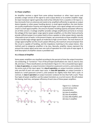
  • 1. 4.1 Power amplifiers An Amplifier receives a signal from some pickup transducer or other input source and provides a larger version of the signal to some output device or to another amplifier stage. An input transducer signal is generally small (a few millivolts from a cassette or CD input or a few microvolts from an antenna) and needs to be amplified sufficiently to operate an output device (speaker or other power handling device). In small signal amplifiers, the main factors are usually amplification linearity and magnitude of gain, since signal voltage and current are small in a small-signal amplifier, the amount of power-handling capacity and power efficiency are of little concern. A voltage amplifier provides voltage amplification primarily to increase the voltage of the input signal. Large-signal or power amplifiers, on the other hand, primarily provide sufficient power to an output load to drive a speaker or other power device, typically a few watts to tens of watts. In the present chapter, we concentrate on those amplifier circuits used to handle large-voltage signals at moderate to high current levels. The main features of a large-signal amplifier are the circuit's power efficiency, the maximum amount of power that the circuit is capable of handling, and the impedance matching to the output device. One method used to categorize amplifiers is by class. Basically, amplifier classes represent the amount the output signal varies over one cycle of operation for a full cycle of input signal. A brief description of amplifier classes is provided next. 4.1.1 Classes of Amplifier Some power amplifiers are classified according to the percent of time the output transistors are conducting, or “turned on.” Four of the principal classifications are: class A, class B, class AB, and class C. These classifications are illustrated in Figure 4.1.1 for a sinusoidal input signal. In class-A operation, an output transistor is biased at a quiescent current ICQ and conducts for the entire cycle of the input signal. For class-B operation, an output transistor conducts for only one-half of each sine wave input cycle. In class-AB operation, an output transistor is biased at a small quiescent current IQ and conducts for slightly more than half a cycle. In contrast, in class-C operation an output transistor conducts for less than half a cycle. These four types of power amplifiers use the output transistors as a current source. We will analyze the biasing, load lines, and power efficiency of each class of these power amplifiers. Figure 4.1.1 Collector current versus time characteristics: (a) class-A amplifier, (b) class-B amplifier, (c) class-AB amplifier, and (d) class-C amplifier
  • 2. 1 4.1.1 Difference between Voltage and Power Amplifier The distinction between voltage and power amplifiers is somewhat artificial since useful power (i.e. product of voltage and current) is always developed in the load resistance through which current flows. The difference between the two types is really one of degree; it is a question of how much voltage and how much power. A voltage amplifier is designed to achieve maximum voltage amplification. It is, however, not important to raise the power level. On the other hand, a power amplifier is designed to obtain maximum output power. Voltage amplifier. The voltage gain of an amplifier is given by ∶ A = β × R R In order to achieve high voltage amplification, the following features are incorporated in such Amplifiers: (i) The transistor with high β (>100) is used in the circuit. In other words, those transistors are employed which have thin base. (ii) The input resistance Rin of the transistor is sought to be quite low as compared to the collector load RC. (iii) A relatively high load RC is used in the collector. To permit this condition, voltage amplifiers are always operated at low collector currents (≈1 mA). If the collector current is small, we can use large RC in the collector circuit. Power amplifier. A power amplifier is required to deliver a large amount of power and as such it has to handle large current. In order to achieve high power amplification, the following features are incorporated in such amplifiers: (i) The size of power transistor is made considerably larger in order to dissipate the heat produced in the transistor during operation. (ii) The base is made thicker to handle large currents. In other words, transistors with comparatively smaller β are used. (iii) Transformer coupling is used for impedance matching. The comparison between voltage and power amplifiers is given below in the tabular form: No Particular Voltage Amplifier Power Amplifier 1 β High(>100) Low (5 to 20) 2 Rc High(4-10k Ω) Low (5 to 20Ω) 3 Coupling Usually R-C Coupling Transformer coupling 4 Input Voltage low (a few mV) High (2-4V) 5 Collector current Low(≈1mA) High(>100mA) 6 Power output Low(≈mW) High(>1W) 7 Output impedance High(≈12k Ω) Low(≈200Ω)
  • 3. 2 4.1.2 Power Amplifier Efficiency Since we are interested in delivering maximum AC power to the load, while consuming the minimum DC power possible from the supply we are mostly concerned with the “conversion efficiency” of the amplifier. Power Amplifier Efficiency η = P P × 100 Where PLoad is the amplifiers output power delivered to the load. Usually we consider RMS Power delivered to a resistive Load for analysis. And PDC is the DC power taken from the supply. 4.1.3 Significance of RMS Value Since the instantaneous power of an AC waveform varies over time, AC power, , is typically measured as an average over time. It is based on this formula = ( ) ( ) For a purely resistive load(R), a simpler equation can be used, based on the root mean square (RMS) values of the voltage and current waveforms: for v(t) = V sinωt, i(t) = v(t) R = V sinωt R = I sinωt, where ω = 2π T P = 1 T v(t)i(t)dt = 1 T V sinωt V sinωt R dt = 1 R 1 T V sin ωtdt From section 4.1.2 we can write = = = Also P = V I = I R = V R = V 2R = I 2 R = V 8R = I 8 R Where V = V √2 = V 2√2 and I = I √2 = I 2√2 and V = 2V and I = 2I
  • 4. 3 Significance of this is that in case of power amplifiers efficiency we are concerned with the power that is delivered to the resistive load when a sinusoidal (current/Voltage is generated across it). So for calculating PLoad we have to use AC power or RMS Power. From the above result it follows that RMS Power (PLoad) is independent of mean value a0 And it depends on the maxim variation a1 only Also for simplicity we are taking T=1 or = in all analysis. But the results are valid for all T and 4.2 Class A Power Amplifier The most commonly used type of power amplifier configuration is the Class A Amplifier. The Class A amplifier is the most common and simplest form of power amplifier that uses the switching transistor in the standard common emitter circuit configuration as seen previously. The transistor is always biased “ON” so that it conducts during one complete cycle of the input signal waveform producing minimum distortion and maximum amplitude to the output. Figure 4.2.1 Typical Class A Amplifier Figure 4.2.1 shows a typical class A amplifier in common emitter configuration. The Voltages Vbb and VCC are input bias voltages used to set the operating point Q. VI is the input voltage and Vo is the output voltage also note that Vo=VCC-ICR Choice of operating Point Q The choice of operating point should be such that it should provide maximum swing at the output. Consider the case of Figure 4.2.2(c ) where the swing is maximum compared with (a) and (b).So the optimum choice of operating point will be at the midpoint VCEQ=VCC/2 to obtain maximum output voltage swing without distortion. In order to get maximum a.c. power output (and hence maximum collector η), the peak value of collector current due to signal
  • 5. 4 alone should be equal to the zero signal collector current IC. In terms of a.c. load line, the operating point Q should be located at the centre of a.c. load line. 4.2.1 Typical Operation We will restrict ourselves to the circuits of this type where the Q remains entirely in the active region. Consider the input Vi to be proportional to sinωt. (i) As Vi↑ IB↑ which implies IC↑ (IC= βIB) Since Vo=(VCC-ICRC) Vo↓. The minimum value of Vo will be just greater than 0 before Q saturates. (ii) As Vi↓ IB ↓ which implies IC↓ (IC= βIB) Since Vo=(VCC-ICRC) Vo↑. The maximum value of Vo will be just below VCC. From the above discussion we can see that Vi and Vo are 1800 out of phase. Consider the maximum value of Vo to VCC and minimum value to 0.(ignore the boundaries) V = V 2 , V ( ) ≈ V and V ( ) = V ( ) ≈ 0 and I = V 2R , I ( ) ≈ V R , I ( ) ≈ 0 Figure 4.2.1.1 Vo vs Vi Also IC and Vo are 1800 out of phase.
  • 6. 5 Figure 4.2.1.2 Vo vs Ic 4.2.2 Efficiency of Class A Amplifier As mentioned before the class A amplifier simply produces a scaled and inverted version of the input. Power Amplifier Efficiency η = P P × 100 Where PLoad is usually the RMS Power (or AC Power delivered to the load R) and PDC is the DC Supply power. Calculating PDC and PLoad We consider only the power supplied by the source VCC. Because the power supplied by source VBB is usually negligible compared with power supple VCC. IC contains two components an (i)AC component and (ii)a DC Component. But it is the time average value of IC that is needed in the calculation of PDC. Since the ideal Q point is at VCC/2 the Ideal ICQ=VCC/(2R) the current I = I + I sin(ωt) 0 ≤ I ≤ V 2R we get the Power supplied by the DC Bias per cycle is 1 T V I dt = 1 T V [I + I sin(ωt)] dt = V I = V 2R since 1 T sin(ωt) dt = 0 For calculating the PLoad the RMS power delivered to load R is considered. Note that IC and Vo is 1800 out of phase but VR (VR=VCC-VO) and IC are in phase. P = P = V I = V R = I R = I √2 R Now η = = R /
  • 7. 6 Now Maximum efficiency η occurs when I = I ( ) = (V )/ (2R) = / = . % Now this 25% is maximum theoretical efficiency with lots of assumptions for a Class A amplifier connected to a purely resistive load. On a practical case the efficiency will be much less because of power consumptions due to VBB, The maximum and minimum value of Vo is not VCC and 0 etc etc. Consequently the usual efficiency observed in Class A Amplifiers is around 10-20%. *4.2.3 Power Flow in Class A Amplifier using Reisitive Loads It is extremely insightfull to calculate the flow of power in this amplifier,beginning from the dc source to the ac power(signal power) delivered to resisitve load. Specifically, power flows from the dc source to both the load and transistor in the form of dc power and ac power (again,ignoring the base circuit). Let’s calculate the maximum of all four of these quantities separately: (a) DC load power. This is due to the time average values of V and I in R and has nothing to due with the time varying component. From Fig. 4.2.1.2: P , = = (b) AC load power. We computed this earlier: P , = (c) DC Transistor Power.The average DC power is same as average DC Powe across Load and has nothing to do with time varying component. Now IQ=VCC/(2R) and VCEQ=VCC/2 hence average DC power across transistor P, = V 2 . V 2R = V 4R (d) AC transistor power. This power is given by the usual expression P, = V I = V ( )I ( ) V 2√2 . − V 2R√2 = − V 8R Note the negative sign in the expression of ICrms because VCE=VO and IC are out of phase by 1800 and hence the power is negative.The negative sign means that transitor supplies the power to the Load. These results from (a) to (d) are pictorially shown in figure 4.2.1.3.
  • 8. 7 Figure 4.2.1.3 Power flow in Class A amplifier 4.2.3.1 Example Problem for better understanding Calculate the (i) output power (ii) input power and (iii) collector efficiency of the amplifier circuit shown in Fig.4.2.3.1.1 (i) It is given that input voltage results in a base current of 10 mA peak. Ans) First draw the d.c. load line by locating the two end points viz., IC (sat) = VCC/RC = 20V/20Ω = 1 A = 1000 mA and VCE = VCC = 20 V as shown in Fig.
  • 9. 8 . The operating point Q of the circuit can be located as under: I = V − V R = 20 − 0.7 1k = 19.3 mA using I = βI we get I = βI = 25 (19.3 mA) = 482 mA Also V = V − I R = 20V − (482 mA) (20 Ω) = 10.4 V The operating point Q (10.4 V, 482 mA) is shown on the d.c. load line. (i) I ( ) = I ( ) = βI ( ) = 25 × 10mA = 250mA P ( ) (I ( )) 2 R = (250mA) 2 × 20Ω = . (ii) P = V I = 20V × 482 mA = 9.6W (iii) = × = . . × = . % 4.2.4 Transformer Coupled Class A Amplifier *Basic transformer operation A transformer can increase or decrease voltage or current levels according to the turns ratio, as explained below. In addition, the impedance connected to one side of a transformer can be made to appear either larger or smaller (step up or step down) at the other side of the transformer, depending on the square of the transformer winding turns ratio. The following discussion assumes ideal (100%) power transfer from primary to secondary, that is, no power losses are considered. Voltage Transformation As shown in Fig. 15.7a, the transformer can step up or step down a voltage applied to one side directly as the ratio of the turns (or number of windings) on each side. The voltage transformation is given by = Above equation shows that if the number of turns of wire on the secondary side is larger than on the primary, the voltage at the secondary side is larger than the voltage at the primary side. Current Transformation The current in the secondary winding is inversely proportional to the number turns in the windings. The current transformation is given by =
  • 10. 9 Impedance Transformation Since the voltage and current can be changed by a transformer, impedance ‘seen’ from either side (primary or secondary) can also is changed. As shown in Fig, impedance RL is connected across the transformer secondary. This impedance is changed by the transformer when viewed at the primary side (RL’). This can be shown as follows: R R = R R = (V / I ) (V / I ) = (V × I ) (I × V ) = (V × I ) (V × I ) = (N × N ) (N × N ) = N N If we define a =N1/N2, where a is the turns ratio of the transformer, the above equation becomes R R = R R = N N = a We can express the load resistance reflected to the primary side as: R = a R or R = a R Where R is the reflected impedance, as shown in above Eqn, the reflected impedance is related directly to the square of the turns ratio. If the number of turns of the secondary is smaller than that of the primary, the impedance seen looking into the primary is larger than that of the secondary by the square of the turns ratio
  • 11. 10 As mentioned in the previous section, there are two major disadvantages of class A amplifiers with resistive loads:  Half of the power from the supply is consumed as dc power in the load resistor.  Some types of loads cannot be connected to this amplifier. For example, a second amplifying stage would have the base of the transistor connected where R is located. The ac voltage would be excessively large for direct connection (typically want ac voltages from 10 – 100 mV or so). An interesting variation of the class A amplifier and one that removes both of these problems is to use a transformer coupled load as shown in Fig. 4.2.4.1: Figure 4.2.4.1 Transformer Coupled Amplifier From this circuit, we can see immediately that there will no longer be any dc power consumed in R since dc does not couple through transformers. Next, notice that the dc resistance between VCC and Q is (nearly) zero so that the average collector voltage VC will then be VCC, not VCC/2 as before. This is very important to understand! The effective load resistance due to Transformer T is given by R’=n2R where n=Np/Ns (Basic transformer knowledge = = = n now R = V i and R = V i and after some simplification we get R = N N R = n R Now RL’=R’+Re ≈ R’ is the effective load seen by transistor not R
  • 12. 11 Under zero signal conditions, the effective resistance in the collector circuit is that of the primary winding of the transformer. The primary resistance has a very small value and is assumed zero. Therefore, d.c. load line is a vertical line rising from VCC as shown in Fig. 4.2.4.2 When signal is applied, the collector current will vary about the operating point Q. Figure 4.2.4.2 ac and dc load Lines With the transformer-coupled load, the maximum VC and IC are now twice as large as with a resistive load: now P = V I = V V R = V R′ Now the ac power delivered to the load is P = 1 2 × V × V R′ = V 2R′ Figure 4.2.4.3 Vc vs Ic for transformer Coupled Class A Amplifier Maximum efficiency η = VCC 2 2R′ / VCC 2 R′ = 0.5 or 50% In other words, the maximum efficiency of the class A amplifier with transformer coupled resistive load is η = 50%.This is twice the efficiency of a class A amplifier with a resistive load. This doubling of efficiency makes sense since we’ve eliminated the dc power to the resistive load.
  • 13. 12 Example for better understanding) A common emitter class A transistor power amplifier uses a transistor with β = 100. The load has a resistance of 81.6 Ω, which is transformer coupled to the collector circuit. If the peak values of collector voltage and current are 30 V and 35 mA respectively and the corresponding minimum values are 5 V and 1 mA respectively, determine : (i) the approximate value of zero signal collector current (ii) the zero signal base current (iii) Pdc and Pac (iv) collector efficiency (v) turn ratio of the transformer. A) In an ideal case, the minimum values of vCE(min) and iC(min) are zero. However, in actual practice,such ideal conditions cannot be realised. In the given problem, these minimum values are 5 V and 1mA respectively as shown in Fig. Note that in this configutation we have bypassed RE using a bypass capacitor.So DC load line is almost vertical
  • 14. 13 (i) The zero signal collector current is approximately half-way between the maximum and minimum values of collector current i.e. Zero Signal I = 35 − 1 2 + 1 = 18mA (ii) Zero Signal I = = = .18mA (iii) Zero Signal V = V = + 5 = 17.5V Since the load is transformer coupled we get VCC≈VCEQ=17.5V DC inout Power P = V I = 17.5 × 18mA = 315mW AC output voltage V ( ) = ( ) √ = √ = 8.84V AC output current I ( ) = ( ) √ = √ = 12mA AC Output Power P = V ( ) × I ( ) = 8.84V × 12mA = 106mW (iv) Power Amplifier Efficiency η = × 100 = × 100 = 33.7% (v) The a.c. resistance R′L in the collector is determined from the slope of the line. Slope = − 1 R = (35 − 1)V (5 − 30)mA = − 34 25 kiloΩ or R = 735Ω we get Turn ratio, n = R R = 735 81.6 = 3
  • 15. 14 Advantages of class-A amplifiers (i) Class-A designs are simpler than other classes; for example class AB and B designs require two connected devices in the circuit (push–pull output), each to handle one half of the waveform; class A can use a single device (single-ended). (ii) The amplifying element is biased so the device is always conducting, the quiescent (small-signal) collector current (for transistors; drain current for FETs or anode/plate current for vacuum tubes) is close to the most linear portion of its transconductance curve. (iii) Because the device is never 'off' there is no "turn on" time, no problems with charge storage, and generally better high frequency performance and feedback loop stability (and usually fewer high-order harmonics). (iv) The point at which the device comes closest to being 'off' is not at 'zero signal', so the problems of crossover distortion associated with class-AB and -B designs is avoided. (v) Best for low signal levels of radio receivers due to low distortion. Disadvantage of class-A amplifiers Class-A amplifiers are inefficient. A theoretical efficiency of 50% is obtainable with transformer output coupling and only 25% with capacitive coupling, unless deliberate use of nonlinearities is made (such as in square-law output stages). In a power amplifier, this not only wastes power and limits operation with batteries, but increases operating costs and requires higher-rated output devices. Inefficiency comes from the standing current that must be roughly half the maximum output current, and a large part of the power supply voltage is present across the output device at low signal levels. If high output power is needed from a class-A circuit, the power supply and accompanying heat becomes significant. For every watt delivered to the load, the amplifier itself, at best, uses an extra watt. For high power amplifiers this means very large and expensive power supplies and heat sinks. Applications Class-A power amplifier designs have largely been superseded by more efficient designs, though they remain popular with some hobbyists, mostly for their simplicity. There is a market for expensive high fidelity class-A amps considered a "cult item" amongst audiophiles mainly for their absence of crossover distortion and reduced odd-harmonic and high-order harmonic distortion.
  • 16. 15 4.3 Harmonic distortion 4.3.1 Amplifier Distortion A pure sinusoidal signal has a single frequency at which the voltage varies positive and negative by equal amounts. Any signal varying over less than the full 360° cycle considered to have distortion. An idea] amplifier is capable of amplifying a pure sinusoidal signal to provide a larger version, the resulting waveform being a pure single-frequency sinusoidal signal. When distortion occurs the output will not be an exact duplicate (except for magnitude) of the input signal. Distortion can occur because the device characteristic is not linear, in which case nonlinear or amplitude distortion occurs. This can occur with all classes of amplifier operation. Distortion can also occur because the circuit elements and devices respond to the input signal differently at various frequencies, this being frequency distortion. One technique for describing distorted but period waveforms uses Fourier analysis, a method that describes any periodic waveform in terms of its fundamental frequency component and frequency components at integer multiples-these components are called harmonic components or harmonics. For example, a signal that is originally 1000 Hz could result, after distortion, in a frequency component at 1000Hz (1 kHz) and harmonic components at 2 kHz (2 X 1 kHz), 3 kHz (3 X 1 kHz), 4 kHz (4 X 1 kHz), and so on. The original frequency of 1 kHz is called the fundamental frequency; those at integer multiples are the harmonics. The 2-kHz component is therefore called a second harmonic that at 3 kHz is the third harmonic, and so on. The fundamental frequency is not considered a harmonic. Fourier analysis does not allow for fractional harmonic frequencies-only integer multiples of the fundamental. 4.3.2 Harmonic Distortion A signal is considered to have harmonic distortion when there are harmonic frequency components (not just the fundamental component). If the fundamental frequency has an amplitude, A1, and the nth frequency component has an amplitude, An a harmonic distortion can be defined as %nth Harmonic Distortion = %D = | | | | × 100 The fundamental component is typically larger than any harmonic component. Q4.3.2.1) Calculate the harmonic distortion components for an output signal having fundamental amplitude of 2.5 V, second harmonic amplitude of 0.25 V, third harmonic amplitude of 0.1 V, and fourth harmonic amplitude of 0.05 V. %D = |A | |A | × 100 = 0.25 2.5 × 100 = 10% %D = |A | |A | × 100 = 0.1 2.5 × 100 = 4% and %D = |A | |A | × 100 = 0.05 2.5 × 100 = 2%
  • 17. 16 4.3.2.1 Total harmonic Distortion When an output signal has a number of individual harmonic distortion components, the signal can be seen to have a total harmonic distortion based on the individual elements as combined by the relationship of the following equation: % = + + × % Q4.3.2.1.1) Calculate the total harmonic distortion for the components given In Q4.3.2.1 Using Computed Values D2=10% D3=4% and D4=2% %THD = D + D + D × 100% = 0.10 + 0.04 + 0.02 × 100% = 10.95% An instrument such as a spectrum analyzer would allow measurement of the harmonics present in the signal by providing a display of the fundamental component of a signal and a number of its harmonics on a display screen. Similarly, a wave analyzer instrument allows more precise measurement of the harmonic components of a distorted signal by filtering out each of these components and providing a reading of these components. In any case, the technique of considering any distorted signal as containing a fundamental component and harmonic components is practical and useful. For a signal occurring in class AB or class B, the distortion may be mainly even harmonics, of which the second harmonic component is the largest. Thus, although the distorted signal theoretically contains all harmonic components from the second harmonic up. The most important in terms of the amount of distortion in the classes presented above is the second harmonic. 4.3.2.2 Second Harmonic Distortion Figure 4.3.2.2.1: Waveform for obtaining second harmonic distortion Figure shows a waveform to use for obtaining second harmonic distortion. A collector current waveform is shown with the quiescent, minimum, and maximum signal levels, and the time at which they occur is marked on the waveform. The signal shown indicates that some distortion is present. An equation that approximately describes the distorted signal waveform is i ≈ I + I + I cosωt + I cos2ωt 4.3.2.2(1)
  • 18. 17 The current waveform contains the original quiescent current ICQ, which occurs with. zero input signal; an additional dc current IO, due to the nonzero average of the distorted signal the fundamental component of the distorted ac signal, I1 ; and a second harmonic component I2, at twice the fundamental frequency. Although other harmonics, are also present, only the second is considered here. Equating the resulting current from 4.3.2.2(1) at a few points in the cycle to that shown on the current waveform provides the following three relations: At point 1 ωt=0 we have i = I = I + I + I cos0 + I cos0 gives I = I + I + I + I At point 2 ωt= π/2 we have i = I = I + I + I cos π + I cos2 π gives I = I + I − I and we get I = I At point 3 ωt= π we have i = I = I + I + I cosπ + I cos2π gives I = I + I − I + I Solving the preceding three equations simultaneously gives the following results: I = I = I + I − 2I 4 and I = I − I 2 By the definition of second harmonic distortion may be expressed as %D = |A | |A | × 100 Inserting the values of I1 and I2 determined above gives D = | 1 2 (Icmax+ICmin)−ICQ ICmax−ICmin | or using voltages D = | 1 2 (Vcmax+VCmin)−VCQ VCmax−VCmin | 4.3.2.3 Power of Signal Having Distortion When distortion does occur, the output power calculated for the undistorted signal is no longer correct. When distortion is present, the output power delivered to the load resistor RC due to the fundamental component of the distorted signal is P = I R 2 The total power due to all the harmonic components of the distorted signal can then be calculated using P = (I + I + ⋯ . ) The total power can also be expressed in terms of the total harmonic distortion P = (1 + D + D + ⋯ . )I R 2 = (1 + THD )P
  • 19. 18 *4.3.2.4 Graphical Description of Harmonic Components of Distorted Signal A distorted waveform such as that which occurs in class B operation can be represented using Fourier analysis as a fundamental with harmonic components. Figure 4.3.2.3.1 shows a positive half cycle such as the type that would result in one side of a class B amplifier. Using Fourier analysis techniques, the fundamental component of the distorted signal can be obtained, as shown in Fig. 4.3.2.4.1 b. Similarly, the second and third harmonic components can be obtained and are shown in Fig 4.3.2.4.1 c and d, respectively. Using the Fourier technique, the distorted Waveform can be made by adding the fundamental and harmonic components, as shown in Fig.4.3.2.3.1 e. In general, any periodic distorted waveform can be represented by adding a fundamental component and all harmonic components, each of varying amplitude and at various phase angles
  • 20. 19 4.4.2 Idealized Class-B Operation Figure 4.4.2.1(a) shows an idealized class-B output stage that consists of a complementary pair of electronic devices. When vI = 0, both devices are off, the bias currents are zero, and vO = 0. For vI > 0, device A turns on and supplies current to the load as shown in Figure 4.4.2.1(b). For vI < 0, device B turns on and sinks current from the load as shown in Figure 4.4.2.1(c). Figure 4.4.2.1(d) shows the voltage transfer characteristics. The ideal voltage gain is unity. Figure 4.4.2.1 (a) Idealized class-B output stage with complementary pair, A and B, of electronic devices; (b) device A turns on for vI > 0, supplying current to the load; (c) device B turns on for vI < 0, sinking current from the load; (d) ideal voltage transfer characteristics
  • 21. 20 4.4.3 Class B push pull circuit with complimentary symmetry Figure 4.4.3.1 shows an output stage that consists of a complementary pair of bipolar transistors. When the input voltage is vI = 0, both transistors are cut off and the output voltage is vO = 0. If we assume a B–E cut-in voltage of 0.6V, then the output voltage vO remains zero as long as the input voltage is in the range −0.6 ≤ vI ≤+0.6 V. If vI becomes positive and is greater than 0.6 V, then Qn turns on and operates as an emitter follower. The load current iL is positive and is supplied through Qn, and the B–E junction of Qp is reverse biased. If vI becomes negative by more than 0.6 V, then Qp turns on and operates as an emitter follower. Transistor Qp is a sink for the load current, which means that iL is negative. Figure 4.4.3.1 This circuit is called a complementary push–pull output stage. Transistor Qn conducts during the positive half of the input cycle, and Qp conducts during the negative half-cycle. The transistors do not both conduct at the same time. Advantages (i) This circuit does not require transformer. This saves on weight and cost. (ii) Equal and opposite input signal voltages are not required. Disadvantages (i) It is difficult to get a pair of transistors (npn and pnp) that have similar characteristics. (ii) We require both positive and negative supply voltages.
  • 22. 21 4.4.3.1 Crossover Distortion From Figure 4.4.3.1.1, we see that there is a range of input voltage around zero volts where both transistors are cut off and vO is zero. This portion of the curve is called the dead band. Figure 4.4.3.1.1 shows the voltage transfer characteristics for this circuit. When either transistor is conducting, the voltage gain, which is the slope of the curve, is essentially unity as a result of the emitter follower. The output voltage for a sinusoidal input voltage is shown in Figure 4.4.3.1.2. The output voltage is not a perfect sinusoidal signal, which means that crossover distortion is produced by the dead band region.Figure 4.4.3.1.2 shows the output voltage for a sinusoidal input signal. When the output voltage is positive, the npn transistor is conducting, and when the output voltage is negative, the pnp transistor is conducting. We can see from this figure that each transistor actually conducts for slightly less than half the time. Thus the bipolar push– pull circuit shown in Figure 4.4.3.1 is not exactly a class-B circuit. Crossover distortion can be virtually eliminated by biasing both Qn and Qp with a small quiescent collector current when vI is zero. This technique is discussed in the next section. Fig 4.4.3.1.1 Voltage transfer characteristics of Figure 4.4.3.1.2 Crossover distortion of basic complementary push–pull output stage complementary push–pull output stage
  • 23. 22 4.4.3.2 Efficiency If we consider an idealized version of the circuit in Figure 4.4.3.1 in which the base–emitter turn-on voltages are zero, then each transistor would conduct for exactly one-half cycle of the sinusoidal input signal. This circuit would be an ideal class-B output stage, and the output voltage and load current would be replicas of the input signal. The collector–emitter voltages would also show the same sinusoidal variation. Figure 4.4.3.2.1 illustrates the applicable dc load line. The Q-point is at zero collector current, or at cutoff for both transistors. The quiescent power dissipation in each transistor is then zero. Fig 4.4.3.2.1 Effective load line of the ideal class-B output stage The output voltage for this idealized class-B output stage can be written as vo=VpSin(ωt) Where the maximum possible value of Vp is VCC.For simplicity we will use T = 2π and ω = 2π = 1 but note that results are valid for all other values of T as well.
  • 24. 23 The instantaneous power dissipation in Qn is p(Qn) = vCEniCn and the collector current is i = v R = V R sin(ωt) for 0 < ωt < π and 0 for π ≤ ωt ≤ 2π where Vp is the peak output voltage. we see that the collector–emitter voltage can be written as vCEn = VCC-VP sin(ωt) Therefore, the total instantaneous power dissipation in Qn is v i or V − V sin(ωt) sin(ωt) for 0 < ωt < π and 0 for π ≤ ωt ≤ 2π The average power dissipation of Qn is 1 (2π) v i dt (2π) = 1 (2π) v i dt (π) Since v i = 0 for π ≤ ωt ≤ 2π The average power dissipation of Qn is = 1 (2π) (V − V sin(ωt)) V R sin(ωt)dt (π) = 1 (2π) V V R sin(ωt)dt − (π) 1 (2π) V sin(ωt)) V R sin(ωt)dt (π) For Simplicity T = 2π we get ω = 2π = 1 and using this in above equation we get 1 (2π) V V R sin(ωt)dt − (π) 1 (2π) V sin(ωt)) V R sin(ωt)dt (π) = − The average power dissipation is therefore = Pavg(Qn) = − The average power dissipation in transistor Qp is exactly the same as that for Qn, because of symmetry. A plot of the average power dissipation in each transistor, as a function of Vp, is shown in Figure 4.4.3.2.2. The power dissipation first increases with increasing output voltage, reaches a maximum, and finally decreases with increasing Vp. We determine the maximum average power dissipation by setting the derivative of Pavg(Qn) with respect to Vp equal to zero, producing dPavg(Qn) dV = V πR − 2V 4R = 0 or V = 2V π and ( ) = =
  • 25. 24 Fig 4.4.3.3.2 Average power dissipation in each transistor versus peak output voltage for class-B output stage Since the current supplied by each power supply is half a sine wave, the average current is 1 (2π) ( V R sin(ωt))dt (π) = V (2πR ) |− [cos(π) − cos(0)]| = V πR Since ω = 2π T and T = 2π The average power supplied by each source is thereforeP = P = V V πR And the total average power supplied by the two sources is 2V V πR The avg power delivered to the load is P (load) = V I = V I √2√2 = V V √2 √2R = 1 2 V R = = × The maximum possible efficiency ηmax occurs when VP=VCC is =. . % This maximum efficiency value is substantially larger than that of the standard class-A amplifier. The actual conversion efficiency obtained in practice is less than the maximum value because of other circuit losses, and because the peak output voltage must remain less than VCC to avoid transistor saturation. As the output voltage amplitude increases, output signal distortion also increases. To limit this distortion to an acceptable level, the peak output voltage is usually limited to several volts below VCC. The maximum transistor power dissipation occurs when Vp = 2VCC/π. At this peak output voltage, the conversion efficiency of the class-B amplifier is, × = . %
  • 26. 25 4.4.3.4 Advantages and Disadvantages Advantages of Class B Amplifier (i) Very low standing bias current. Negligible power consumption without signal. (ii) Can be used for much more powerful outputs than class A (iii) More efficient than Class A. Disadvantages of Class B Amplifier (i) Creates Crossover distortion. (ii) Supply current changes with signal, stabilized supply may be needed. Because the large and varying current drawn by a powerful class B amplifier also puts considerable extra demand on the DC power supply. (iii) More distortion than Class A. Applications Single ended Class B amplifiers are not used in present day practical audio amplifier application and they can be found only in some earlier gadgets. Another place where you can find them is the RF power amplifiers where the distortion is not a matter of major concern. Anyway, Class C amplifiers are more often used in RF power amplifier applications. 4.4.4 Class AB amplifier Crossover distortion can be virtually eliminated by applying a small quiescent bias on each output transistor, for a zero input signal. This is called a class-AB output stage and is shown schematically in the circuit in Figure 4.4.4.1. If Qn and Qp are matched, then for vI = 0, VBB/2 is applied to the B–E junction of Qn, VBB/2 is applied to the E–B junction of Qp, and vO = 0. The quiescent collector currents in each transistor are given by i = i = I e / = I e / Fig 4.4.4.1 Bipolar class-AB output stage Figure 4.4.4.2 Characteristics of a class-AB o/p stage:
  • 27. 26 As vI increases, the voltage at the base of Qn increases and vO increases. Transistor Qn operates as an emitter follower, supplying the load current to RL. The output voltage is given by V = V + − v and the collector current of Qn (neglect base currents) is i = i + i Since iCn must increase to supply the load current, vBEn increases. Assuming VBB remains constant, as vBEn increases, vEBp decreases resulting in a decrease in iCp. As vI goes negative, the voltage at the base of Qp decreases and vO decreases. Transistor Qp operates as an emitter follower, sinking current from the load. As iCp increases, vEBp increases, causing a decrease in vBEn and iCn. Figure 4.4.4.2(a) shows the voltage transfer characteristics for this class-AB output stage. If vBEn and vEBp do not change significantly, then the voltage gain, or the slope of the transfer curve, is essentially unity. A sinusoidal input signal voltage and the resulting collector currents and load current are shown in Figures 4.4.4.2(b), (c), and (d). Each transistor conducts for more than one-half cycle, which is the definition of class-AB operation. There is a relationship between iCn and iCp. We know that vBEn + vEBp = VBB which can be written V ln i I + V ln i I = 2V ln I I i i = I The product of iCn and iCp is a constant; therefore, if iCn increases, iCp decreases, but does not go to zero. Also using i = i + i and i i = I we get i − i i − i = 0 From the equations above, we can see that for positive output voltages, the load current is supplied by Qn, which acts as the output emitter follower. Meanwhile, Qp will be conducting a current that decreases as vO increases; for large vO the current in Qp can be ignored altogether. For negative input voltages the opposite occurs: The load current will be supplied by Qp, which acts as the output emitter follower, while Qn conducts a current that gets smaller as vI becomes more negative. Equation or i i = I ,relating icn and ipn, holds for negative inputs as well. The power relationships in the class AB stage are almost identical to those derived for the class B circuit. The only difference is that under quiescent conditions the class AB circuit dissipates a power of VCCICQ per transistor. Since IQ is usually much smaller than the peak load current, the quiescent power dissipation is usually small. Nevertheless, it can be taken into account easily. Specifically, we can simply add the quiescent dissipation per transistor to its maximum power dissipation with an input signal applied, to obtain the total power dissipation that the transistor must be able to handle safely.
  • 28. 27 Since, for a zero input signal, quiescent collector currents exist in the output transistors, the average power supplied by each source and the average power dissipated in each transistor are larger than for a class-B configuration. This means that the power conversion efficiency for a class-AB output stage is less than that for an idealized class-B circuit. In addition, the required power handling capability of the transistors in a class-AB circuit must be slightly larger than in a class-B circuit. However, since the quiescent collector currents ICQ are usually small compared to the peak current, this increase in power dissipation is not great. The advantage of eliminating crossover distortion in the class-AB output stage greatly outweighs the slight disadvantage of reduced conversion efficiency and increased power dissipation. Advantages of Class AB power amplifier.  No cross over distortion.  No need for the bulky coupling transformers.  No hum in the output. Disadvantages of Class AB power amplifier.  Efficiency is slightly less when compared to Class B configuration.  There will be some DC components in the output as the load is directly coupled.  Capacitive coupling can eliminate DC components but it is not practical in case of heavy loads. Applications: ECM/EW Jammers Booster Amplifiers Transmitters RFI/EMI Testing High Power TWT Replacements Visual Television Amplifiers High Power Calibration Testing