
Recommended
Recommended
More Related Content
Similar to Novel conservative reversible error control circuits based on molecular QCA
Similar to Novel conservative reversible error control circuits based on molecular QCA (20)
More from VIT-AP University
More from VIT-AP University (20)
Recently uploaded
Recently uploaded (20)
Novel conservative reversible error control circuits based on molecular QCA
- 1. Int. J. Computer Applications in Technology, Vol. 56, No. 1, 2017 1 Copyright © 2017 Inderscience Enterprises Ltd. Novel conservative reversible error control circuits based on molecular QCA Neeraj Kumar Misra* Department of Electronics Engineering, Institute of Engineering and Technology, Lucknow, India Email: neeraj.mishra@ietluckow.ac.in *Corresponding author Bibhash Sen Department of Computer Science and Engineering, National Institute of Technology, Durgapur, India Email: bibhash.sen@cse.nitdgp.ac.in Subodh Wairya Department of Electronics Engineering, Institute of Engineering and Technology, Lucknow, India Email: swairya@ietlucknow.edu Abstract: Quantum-dot cellular automata are a prominent part of the nanoscale regime. They use a quantum cellular based architecture which enables rapid information process with high device density. This paper targets the two kinds of novel error control circuits such as Hamming code, parity generator and checker. To design the HG-PP (HG = Hamming gate, PP = parity preserving), NG-PP (NG = new gate) are proposed for optimising the circuits. Based on the proposed gates and a few existing gates, the Hamming code and parity generator and checker circuits are constructed. The proposed gates have been framed and verified in QCA. The simulation outcomes signify that their framed circuits are faultless. In addition to verification, physical reversible is done. The reversible major metrics such as gate count, quantum cost, unit delay, and garbage outputs, uses best optimisation results compared to counterparts. They can be utilised as a low power error control circuit applied in future communication systems. Keywords: reversible computing; quantum cost; conservative gate; hamming code; parity generator and checker; quantum-dot cellular automata; error control. Reference to this paper should be made as follows: Misra, N.K., Sen, B. and Wairya, S. (2017) ‘Novel conservative reversible error control circuits based on molecular QCA’, Int. J. Computer Applications in Technology, Vol. 56, No. 1, pp.1–17. Biographical notes: Neeraj Kumar Misra is pursuing a PhD program under TEQIP-II in the Department of Electronics Engineering at the Institute of Engineering & Technology (IET) Lucknow, India. He completed his BTech in Electronics and Communication Engineering from Integral University and MTech from Amity University, in 2008 and 2012 respectively. His research interests include reversible logic, fault-tolerant digital design, quantum-dot cellular automata, circuit and architectures for emerging nanotechnology, low power VLSI. Bibhash Sen received the PhD, MTech and BTech degree in Computer Science and Engineering from IIEST Shibpur, BESU Shibpur and NERIST, Nirjuli, India in 2015, 2007 and 2002 respectively. He also worked for Cognizant Technology Solution, India from 2007 to 2008. He is now working as Assistant Professor at National Institute of Technology Durgapur, India since 2008. His research interests includes design and Testing of a digital circuit based on QCA and reversible logic, a fault-tolerant architecture for emerging nanoelectronics. Subodh Wairya is a Professor and Head of the Department of Electronics Engineering at the Institute of Engineering & Technology (IET) Lucknow, India. He has completed his doctoral degree from Motilal Nehru National Institute of Technology, Allahabad, India and received his ME (Telecommunication) from Jadavpur University, Kolkata and BTech (Electronics Engineering.) from H.B.T.I., Kanpur, India. His major research interests include digital circuits,
- 2. 2 N.K. Misra, B. Sen and S. Wairya high-speed network, and NANO-Electronics. He has more than 22 years’ experience in teaching and research. He has served as Scientist ‘B’ in Defense Research & Development Organization (DRDO) and Graduate Engineer (Design Project) in Hindustan Aeronautical Limited (HAL), Lucknow from 1994 to 1996. 1 Introduction In recent years, low power becomes a primary factor due to the advancement in an integrated circuit. In 1960, Landauer proved that the energy dissipated due to loss of data bits is related to the irreversible logic circuit (Landauer, 1961). It has been also presented that the energy dissipated is exactly (n*KTln2), where n = total sum of the data bits loss, K = Boltzmann’s constant and T = temperature. Bennett proves that the ideally zero energy dissipation can be possible if the circuit is designed by the reversible gate (Bennett, 1973). Reversible logic has become one of the most popular techniques owing to the reduced energy dissipation. Further, the quantum circuit, as the enormous area (Wille, 2011), designs the reversible circuit. The nature of quantum circuit is reversible (Sen et al., 2014). Thus, computing using quantum circuit shows an attractive prospect for next generation technology. A significant action in reversible circuit design is the optimisation of parameters such as garbage outputs, gate count, constant input, unit delay, and quantum cost for efficient circuit design (Sen et al., 2013; Misra et al., 2017a). A popular area of nanoelectronics is a regime which is not met by the MOS transistor technology due to its feature size reduction (Nehru and Shanmugam, 2014; Pankaj et al., 2016). In this way, quantum-dot cellular automata (QCA) approach the practice of high computation speed, low power, and high density (Mohammadyan et al., 2015). It is a good vision to use QCA technology in digital logic circuit design (Misra et al., 2016a). Conservative logic based circuits can find the error by matching the parity bits (Roohi et al., 2016; Misra et al., 2017b). In data communication environment the data bits are transmitted from the transmitter to the receiver over a noisy medium. In the way, the Hamming code was proposed by Richard W. Hamming in the 1940s (Misra et al., 2015). Hamming code based error detection and correction are still receiving more consideration for research as well as industry. Its outstanding feature is to detect and correct the error (Haghparast and Navi, 2011; Misra et al., 2016b). The primary challenge of Hamming circuit is to develop low reversible metrics on quantum computing framework (Misra et al., 2016a). To the best of state-of-art review technology, this is a first attempt in the literature that successfully synthesises Hamming code circuit with the optimising reversible metrics. In nano-communication application, the main challenge is to make error-free data communication (Jayanthy et al., 2013; Gupta et al., 2015). In a more practical way, the reversible circuit is more useful in nano-communication, when we minimise reversible metrics. It is reviewed that reversible circuit having include of conservative logic gates is more demand (Chandra et al., 2015). In our work, we minimise the reversible metrics in conservative reversible logic based circuit, it is successfully achieved as reported here. This work concentrates on the error control circuits, which is showing a Nano-communication framework. The existing circuit in Thapliyal and Ranganathan (2010), Das and De (2016), Haghparast and Navi (2011), Mustafa and Beigh (2013), and Ahmad et al. (2015) motivates the circuit. We design first category circuit like a conservative reversible hamming code. The second category of conservative reversible circuit such as parity generator and parity checker. To optimise our designs, we propose two novel conservative, reversible gates such as HG-PP (HG = Hamming gate, PP = parity preserving), and NG-PP (NG = new gate) gates for circuits synthesis and optimisation. In addition, the quantum equivalent is presented for all the proposed circuits. The error control circuits like Hamming code, parity generator, and parity checker provided full coverage of error control. The justification of parity generator and parity checker logic circuit are constructed by novel NG-PP gate, whereas Hamming code circuit is based on novel HG-PP gate. The QCA implementations of the novel gates are also presented to justify the reliability of circuit in the physical foreground. The proposed circuits are superior in terms of reversible metrics such as quantum cost, unit delay, garbage output, constant input, and gate count. In addition, the quantum equivalent is presented to all the proposed error control circuits. Moreover, we estimate the energy dissipation related parameters of proposed gates by using the QCAPro tool, to indicate the low power feature in the work. Especially, this workaround in reversible error control circuits can be highlighted as: The proposed conservative reversible gates such as HG- PP and NG-PP are taken into consideration for the design of Hamming code, parity generator, and parity checker. An attempt has been made to design the quantum equivalent circuits for error control circuit. The workability of the proposed gates is justified by QCADesigner, which shows the property under an environment of majority gates, and inverter to meet the physical foregrounds. We use a few novel reversible gates to account for the low-cost metrics in the circuit model of error control circuits and compare the cost metrics to existing counterparts. These comparative results lead to very low reversible metrics reported here.
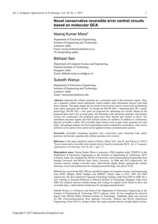
- 3. Novel conservative reversible error control circuits based on molecular QCA 3 We described the energy dissipation of proposed gates such as HG-PP and NG-PP by designing a thermal layout in QCAPro tool. The work is organised as follows: Section 2 presents the QCA fundamentals including the reversible logic. The state-of-the-art section is framed in Section 3. Section 4 proposes two novel reversible gates. Section 5 includes the proposed gates in QCA framework. Section 6 contains energy dissipation analysis of proposed gates. Section 7.1 shows synthesis approach of parity generator and checker. Section 7.2 presents the proposed circuits of Hamming generator and checker. Section 7.2.3 presents the observation and discussion. Finally, the conclusion is presented in Section 8. 2 QCA fundamentals and reversible logic In this section, we present the fundamentals of QCA including reversible logic, conservative logic, and quantum cost. 2.1 QCA A QCA cell contains four dots with two free electrons (Lent et al., 1993). The two polarisation states (P = –1, P = +1) are possible as per the electrons location in the cell (Figure 1a). In QCA two fundamental structures are possible as an inverter and the majority, as depicted in Figure 1b, 1c. QCA clock has four clock zones (clock0, clock1, clock2 and clock3) each clock phase shifted by 90°. Each clock zone has four phases (Release, relax, switch and hold), as shown in Figure 1d, 1e. The clock phase’s description as switch phase: barrier is gradually high, hold phase: polarity withholds, release: barrier is gradually lowered, relax: release polarity, as shown in Figure 1f. The Coulombic attraction between nearest electrons leads to synchronisation of adjacent cells, so they affect the polarisation state of another cell (Das et al., 2012). Thus, a repeated cell arrangement in QCA forms a wire. The QCA complements or un-complement signal of input are realised by the alternate arrangement of cells by tapping off a normal wire (Figure 1g). 2.2 Reversible logic In reversible logic gate there is a bijective property (unique correspondence) between the input and the output vectors in function F (F has n x n type, where n = input and n = output) then F is reversible. It is only the gate level designing approach. The reversible gate is essential units of the reversible logic circuit (Tabatabaii and Haghparast, 2016). The delay is the maximum number of the gate in a path from applying input to target output line. It is considered that each gate executes computation in the one-time unit. Figure 1 Basics of QCA (a) four-dot QCA cell (b) inverter (c) majority gate (d) clock, four stages (e) clock phase shifted (90°) (f) clocking concept (g) outputs, realisation from inputs 0 45 0 90 0 90 2.3 Conservative reversible logic A conservative gate is a reversible gate that regularly fixes the parity between inputs and outputs. More appropriately, a n x n conservative reversible gate preserves the parity as well as the unique mapping between all sequences of inputs and outputs (Misra et al., 2016c). 2.4 Quantum cost The count of controlled-V, controlled-V+ , and Ex-OR, gates gives the total quantum cost of the quantum circuit. The representation of controlled-V is shown in Figure 2a. If the control input A=0, qubit B will propagate through the A will remain the same i.e., Q=B is synthesised. Another value of controlled input A=1 then the unitary operation applies to the other input B, that is Q = V (B). The other quantum gate is controlled V+ gate is depicted in Figure 2b. If control input A=0 means qubit B will propagate but a controlled part, remain the same i.e., Q=B. Another value of A=1 means unitary operation V+ =V– applies to the input B i.e., Q=V+ (B). The three types of quantum equivalent are depicted in Figure 2c. The equivalent quantum cost of these
- 4. 4 N.K. Misra, B. Sen and S. Wairya qubit gates is zero. The two other integrated qubit gate is illustrated in Figure 2d. The basic properties V x V=NOT, V+ x V =V x V+ =I, V+ x V+ =NOT were utilised for reversible computing. Figure 2 Basic quantum gates (a) square root of NOT (b) Hermitian matrix of SRN (c) quantum wire (d) integrated qubit 1 I 2 I 1 I ) I ( V 2 2 I 1 I V 1 I 2 I 1 I ) I ( V 2 2 I 1 I V 1 I 2 I 1 I 2 1 I I 1 I 2 I 1 I 2 I 1 I 2 I 1 I 2 I V V V V ) a ( ) b ( 1 Cost 0 Cost 0 Cost 1 Cost 1 Cost ) c ( ) d ( Table 1 Previous works on reversible error control Circuit Need Method Factor Surround HGC in Haghparast et al. F2G R/C More CC and UD Missing HGC in Haghparast et al. F2G R/C More QC and GO Missing HGC, circuit #1in James et al. FG, HCG R More GC and QC Missing HGC, circuit #2 in James et al. FG, F2G R More CC Missing HGC, circuit #3 in James et al. F2G, PPHCG R/C More CC Missing HGC, circuit #4 in James et al. F2G R/C More CC and UD Missing HDC, circuit #5 in James et al. HCG, FG R More GO Missing HDC, circuit #6 in James et al. F2G R/C More CC and UD Missing PGC in Mustafa et al. FG R More QC and GO QCA PGC in Ahmed et al. Logic gates NR More latency, CC and area QCA Notes: HGC-Hamming generator circuit; HDC-Hamming detector circuit; PGC-Parity generator circuit; R/C- Reversible/Conservative; NR-Non-reversible; CC-Circuit complexity; UD-Unit delay; QC-Quantum cost; GO- Garbage outputs; GC-Gate count; QC-Quantum cost. 3 Related work On the synthesis of error control circuits, less amount of research works presented in the state-of-the-art work. The design in Das and De (2016) has addressed reversible parity generator and checker circuits using Feynman gate (FG) there is a certain limitation. Firstly: circuits claim too much gate count, garbage outputs, and quantum cost. Secondly: circuits are non-conservative. The design in (James et al., 2007) has discussed the Hamming code based approach to error control in reversible circuits. The presented approach target both in parity based gates and without parity based gates. The cost for such without parity based Hamming-code generator was GC of 6 gate and quantum cost of 8, the Hamming code detector requires GC of 4 and QC of 9. The parity-based Hamming- generator used GC of 6 and quantum cost of 12, Hamming- checker requires GC of 5 and QC of 10. Most of the existing designs focused only on the reversible circuits synthesise without emphasis on the nanometric scale such as QCA technology. We considered the most optimised Hamming error control circuits in Haghparast and Navi (2011), James et al. (2007) and parity generator and checker circuits in Das et al. (2012) and compared it with our circuits, as an achievement in both circuits were to reduce the reversible metrics. 4 The proposed reversible gates For construction and optimisation of reversible circuits, we have proposed few conservative reversible gates. 4.1 Conservative reversible HG-PP gate A 5 x 5 conservative reversible logic gate named HG-PP is drawn in Figure 3a.The truth table of HG-PP is drawn in Figure 3c. It depicts the same count of 1’s in the output as well as input, further maintain the bijective-mapping property of the reversibility. Hence this gate is reversible as well as conservative. The quantum equivalent and HG- PP.tfc is depicted in Figure 3b. The QC of HG-PP gate is only four, as shown in Figure 3b. This work designs HG-PP because it can helpful for the design of hamming code. The LC of HG-PP is calculated in this method. The R, and T expressions have LC = 0. Then final LC can be computed as: LC (HG-PP) = 2α (P) + 1α (Q) + 0α (R) + 1α (S) + 0α (T) = 4α. The utility of the HG-PP gate as a reversible three input Ex- OR, two input Ex-OR, and signal duplication, if applying the inputs. This work design HG-PP because it can easily construct the conservative reversible hamming generator and checker circuit with utilising very less quantum cost and gate count.
- 5. Novel conservative reversible error control circuits based on molecular QCA 5 4.2 Conservative reversible NG-PP gate The NG-PP structure is utilised of 5-input and 5-output. The schematic diagram and truth table is shown in Figures 4a, 4b. By seeing the truth table the input parity to output parity is conserved. Hence this gate is a conservative gate. Further, it holds the bijective mapping, it also the reversible gate. The QE of NG-PP is shown in Figure 4c. This work designs NG-PP because it can singly perform the logic operation of parity generator and checker. The LC of NG-PP is calculated in this method. The P, Q, and R expressions have LC = 0. The S expression (ABC) has LC =3α. Then we form signal duplication to make (ABC) in T expression. Then final LC can be computed as: LC (NG-PP) = 0α (P) + 0α (Q) + 0α (R) + 1 α (for signal duplication operation in T) + 3α (S) + 1α (T) = 5α. Now we have presented the utility of NG-PP by setting D=E=0, the same time realise the three input Ex-OR logic function with only use of QC of 5, which are useful for the construction of conservative reversible parity generator and parity checker circuit. Throughout the work we measure the quantum cost: It is the number of elemental quantum gates involve in the quantum circuit. In all the schematic diagram in this work we consider inputs are all on the left side, where the corresponding outputs on the right side. Throughout the work we include the *.tfc code to synthesise the quantum equivalent as well as quantum cost. Moreover, the manual manipulation of the quantum cost is also done to ensure the correct value of quantum cost. Throughout the work we try to minimise the quantum cost is beneficial for quantum computing paradigm. 5 Design of proposed gates in QCA framework The idea of the logic design of reversible computing in QCA technology is based on the fact that the addition of reversible circuits with QCA framework is equivalent to the low power circuit. QCA technology is considered as the following features such as high-speed computing, high device density, and low energy dissipation. The QCA cells are used for implementing the QCA circuit. The basic building elements of the QCA circuit are the majority voter gate, inverter, and wire. Figure 3 The proposed conservative reversible HG-PP (a) schematic diagram (b) HG-PP. tfc code and QE (c) truth table HG-PP .v A,B,C,D,E .i A,B,C,D,E .o A,B,C,D,E BEGIN T2 C,A T2 E,A T2 C,B T2 E,D END 1 2 3 4 (a) (b) (c)
- 6. 6 N.K. Misra, B. Sen and S. Wairya Figure 4 The proposed conservative reversible NG-PP (a) schematic diagram (b) NG-PP. tfc code and QE (c) truth table NG-PP .v A,B,C,D,E .i A,B,C,D,E .o A,B,C,D,E BEGIN T2 D,E T2 B,D T2 A,D T2 C,D T2 D,E END NG-PP.tfc code (a) (b) (c) The novel gates are tested in QCADesigner tool. The simulating computer is provided with Intel(R) core(TM) i5- 6200U CPU 2.40GHz, 4GB RAM, and environment of Window 10Home (64-bit). Addition, the simulation setting (Bistable approximation) of QCADesigner have been adopted with dot diameter, single cell area, adjacent cell distance, radius of effect, and cell separation, which is settled to be 5nm, (18nm) x (18nm), 42nm, 65nm, and 2nm respectively. The novel gates are designed with QCADesigner tool for checking the workability and further the QCA primitives are evaluated. The characteristics of QCA primitives like cell complexity, area, and latency are also evaluated. The workability has ensured the implementation in QCA show the existence in the physical foreground. 5.1 Design of NG-PP gate in QCA In order to check the workability of the proposed NG-PP in QCADesigner. First, the layout of NG-PP is implemented in QCA. The NG-PP cell layout, a block diagram with clock zone and simulation result are depicted in Figures 5a, 5b, and 5c. The simulation result ensures the correctness of the gate. The simulation result is checked by comparing with truth table as drawn in Figure 4c. The QCA layout of NG- PP is implemented with majority voter gates of 9, inverters of 6, and area of 45nm2 . 5.2 Design of HG-PP gate in QCA The prominent application of reversible circuit in QCA computing is a nanoscale based computing. The block diagram, cell layout, and the simulation result of HG-PP are shown in Figures 6a, 6b, and 6c. It is remarkable that the latency of the design has been decreased by using the QCA layout. In Figure 6c simulation result is verified. The simulation result is justified by comparison with truth table as drawn in Figure 3c. By the results analysis, it is noticed that the proposed HG-PP layout achieved cell complexity of 175, area of 0.25 µm2 , and latency of 3. 5.3 The performance table of proposed gates regarding QCA primitives In summary, the QCA primitive’s results of proposed gates in terms of majority voter (MV), latency, total area, cell area and area usages are presented in Table 2. The QCA primitive’s results are justified by the QCA layout. The area of one QCA cell is expressed as: (18nm) x (18nm) = 324 nm2 . The approach of area usages and cell area calculation are described below as: Cell area = (Total cell) x (One cell area) Area usage = (Cell area) / (Total area) = (Total cell) x (One cell area) / Total area Thus the area usages calculated of proposed gates are calculated as: 1 Area usages of HG-PP = (173) x (324) / 241057 x 100 % = 23.25 %, 2 Area usages of NG-PP = (255) x (324) / 422254 x 100 % = 19.56 %.
- 7. Novel conservative reversible error control circuits based on molecular QCA 7 Figure 5 QCA implementation of NG-PP (a) block diagram (b) cell layout (c) simulation result D3 D3 D0 D2 D1 D2 D1 D2 D1 D0 C D2 D1 D2 D1 D3 D0 B D A D0 D0 D2 D1 -1 +1 D1 D1 -1 D2 D3 D0 -1 D2 D1 D3 D0 D2 E D0 -1 D1 +1 T S D2 D1 D3 D3 D3 (a) (b) (c) Figure 6 QCA implementation of HG-PP (a) block diagram (b) cell layout (c) simulation result D3 D3 D0 D2 D1 D2 D1 D2 D1 D0 D2 D1 D2 D1 D3 D2 D2 D3 D1 D0 D1 P Q +1 -1 D1 B -1 A D2 D2 D3 D1 D0 D1 S +1 -1 D1 D -1 D0 C D0 D0 E D0
- 8. 8 N.K. Misra, B. Sen and S. Wairya Table 2 QCA primitive’s results of proposed gates Gates QCA Primitives MV L CC TA (nm2 ) CA (nm2 ) AU % HG-PP 8 3 173 241057 56052 23.25 NG-PP 9 4 255 422254 82620 19.56 Notes: MV: Majority voter gate, L: Latency (Clock delay), CC: Cell count: TA: Total area, CA: Cell area, AU: Area usage. Thus the results of table ensure that the proposed gates QCA layouts have met the demand of nanoscale QCA based computing. 6 Energy dissipation analysis Energy dissipation of QCA layout is important in the low power paradigm. Reduced energy dissipation and improve efficiency are important in nanoelectronics application. Researcher in Srivastava et al. (2009) proposed an energy estimation model to the QCA circuit based on kink energy. This model shows the effect of kink energy on energy dissipation on the sharp clock transitions. The thermal layout and energy dissipation related parameters are performed on the Intel (R) core(TM) i5- 6200U CPU 2.40GHz, 4GB RAM, and environment of Linux (Ubuntu-12.04, 32bit). We have taken files such as *. QCA file (create in QCADesigner version 1.4.0), majority switching vector (only inputs), and majority vector set (both inputs and outputs). These files are implemented in QCAPro tool to find the energy dissipation related parameters like switching energy dissipation, average energy, maximum and minimum energy dissipation, and thermal layout. The thermal layout has the unique design of visualising the energy dissipation at each cell. The cells have two colours. The darker cells have more the energy dissipation and vice versa. Thus lighter cells have now become dominate the thermal layout, whereas darker cell is few numbers. 6.1 Energy dissipation estimation for HG-PP and NG-PP Towards estimation of energy dissipation, we first illustrate the kink energy. The kink energy is affected the energy dissipation. In fact, the two adjacent cells have opposite polarisation the energy dissipation increase and the increased energy is known as kink energy (always greater than ground energy). In fact, minimum energy is termed for same polarisation state and maximum for different polarisation state. In this work, a model in Srivastava et al. (2009) is adopted for the result of energy estimation. The thermal layout map for energy dissipation in each cell of NG-PP is shown in Figure 7a, which shows the maximum number of cells is dissipated less energy (lighter cells). The energy dissipated parameters for NG-PP is visualised in Figure 7b. In the 0.5Ek, max. energy diss., min. energy diss., avg. energy diss., avg. leakage, and avg. switching energy diss. are 0.01837, 0.07365, 0.58932, 0.28173, 0.1362 respectively, likewise are 0.37631, 0.21735, 0.71635, 0.35672, 0.38965 respectively at 1Ek, and 0.47325, 0.36271, 0.97632, 0.31782, 0.76532 respectively at 1.5Ek. This energy dissipation analysis and QCA primitive’s results ensure the high demand of NG-PP gate in the nanoelectronics paradigm. The energy dissipated related results for HG-PP is depicted in Figure 8b. This result shows the max. energy diss., min. energy diss., avg. energy diss., avg. leakage, and avg. switching energy diss. are 0.01307, 0.09844, 0.28008, 0.09934, 0.18074 respectively at 0.5Ek, likewise are 0.59504, 0.27176, 0.42273, 0.27404, 0.14869 respectively at 1Ek, and 0.72997, 0.46136, 0.58710, 0.46430, 0.12280 respectively at 1.5Ek. By this result, the avg. energy diss. of the HG-PP increase with the kink energy in a constant manner. Figure 8a shows the thermal layout map for energy dissipated in each cell of an HG-PP. Figure 7 NG-PP (a) thermal layout map (b) energy dissipation results (a) (b)
- 9. Novel conservative reversible error control circuits based on molecular QCA 9 7 The proposed conservative reversible error control circuits In this section, we present two nano-communication circuits such as Hamming code, even parity generator and even parity detector. 7.1 The proposed circuit of even parity generator and even parity checker In this section, we demonstrate synthesis of conservative reversible circuits such as even parity generator and even parity checker in quantum computing paradigm. Figure 8 HG-PP (a) thermal layout map (b) energy dissipation results (a) (b) Figure 9 NG-PP based realisation of (a) parity generator (b) parity checker NG-PP NG-PP Parity Generated bit Parity checker bit Even Parity Generator Even Parity Checker a b
- 10. 10 N.K. Misra, B. Sen and S. Wairya Figure 10 Complete schematic of parity generator and checker NG-PP NG-PP Transmission wire No Error Error Detection Circuit a b 7.1.1 Even parity generator There is vast potential to control error when applying parity generator and checker to a data communication system (Mustafa and Beigh, 2013). Even parity generator is a circuit that finds the input data bits, performs the Ex-OR operation to all the input data bits then determine the even number of 1’s, which is studied in Ahmad et al. (2015). The parity generator (Pg) bit is 1 when the number of 1’s is even, otherwise not. This parity generator circuit contains one NG-PP gate. The inputs contain three data bits (D0, D1, D2) and two constant inputs, which is shown in Figure 9a. This circuit can be programmed by applying data bits. The parity generator bits are expanded as g 0 1 2 P D D D . It is clear from the Figure 9a the output bit is high when even numbers of 1’s appear. 7.1.2 Even parity checker The structure of proposed even parity checker is presented in Figure 9b. This circuit contains one gate (NG-PP), it requires five inputs and five outputs. The input contains four data bits (D0, D1, D2), one parity generator bit (Pg), and one CI. This circuit produces four outputs (D0, D1, D2, Pg) and one GO. In addition, parity checker bit is synthesised by Ex-OR of inputs. However, when the parity checker bit (PC) is low, the no error condition occurs. If the case of checker bit (PC) is high, then there occurs an error in receiving data bits. This circuit also captures all the data bits (D0, D1, D2) on the output side, an attractive technique for online testability of circuit. The error detector circuit is synthesised by two gates (two NG-PP), it requires six inputs and six outputs. The inputs contain three data bits ((D0, D1, D2), and two CI. The circuit produces four outputs: D0, D1, D2, which are recovered data bits, and Pc which is indicated for an error condition. This circuit has three CI, and two GO, as depicted in Figure 10b. In this circuit construction, we report the algorithm 1. Algorithm 1: Complete parity generator and checker Input, Output: Inputs data bits (D0, D1, D2) in binary form, Outputs Pc in binary form. 1: For i=0 to n-1 do 2: If i=1 then (D0, D1, D2, 0, 0) → NG-PP // Assign inputs to first NG-PP NG-PP ← (D0, D1, D2, Pg) // Catch three intermediate outputs End if, Else 3: (D0, D1, D2, Pg) → NG-PP // Assign inputs to second NG-PP (Pc) ← NG-PP // Catch the one outputs End if, Else 4: If i = 3 then Call desired output (Pc) ← NG-PP // Desired output End if, Else 5: If Pc=0 then Comment: No Error End if, Else Comment: Error NG-PP← (GO1), NG-PP← (GO2) // Remaining as GO 6: End if, end for, 7: Return Pc, End;
- 11. Novel conservative reversible error control circuits based on molecular QCA 11 Proposition 1. The LC of the complete even parity generator and checker is LC (complete even parity generator) = 2LC (NG-PP) = 2 x 5α = 10α. Proposition 2. The QC of the complete even parity generator and checker is QC (complete even parity generator) = 2 QC (NG-PP) = 2 x 5 = 10. In the state-of-the-art work, there are fewer circuits of conservative reversible (CR), parity generator and checker. The circuit proposed in Das and De (2016) shows the optimised circuit of parity generator and checker but non- conservative approach. Table 3 presents the performance of our circuit versus counterpart works. 7.1.3 Simulation results for even parity generator and checker Lemma 1: The proposed 3-bit parity generator and 4-bit parity checker are required 1.5 latency. Proof: The 3-bit parity generator contains one NG-PP gate (in Figure 9a). The inputs include three data-inputs (D0, D1, D2) to various combinations of binary value, the generated outcome (Pg) result is obtained after 1.5 cycle delay, as shown in Figure 11. Hence a 3-bit parity generator is required at least 1.5 latency. A 4-bit parity checker circuit is shown in Figure 9b. The inputs include four data-inputs (D0, D1, D2, Pg) and one constant input as logic ‘0’. The circuit is utilised same as QCA layout of NG-PP gate. The simulation outcomes is shown in Figure 12. This outcome is justified by comparing the truth table as drawn in Figure 9b. The required parity checker is obtained after 1.5 clock cycle delay. Hence a parity checker has required at least 1.5 latency. 7.2 The proposed circuit of hamming generator and checker In this section, we have illustrated our compact circuit for hamming generator and checker using novel reversible gate and few existing gates. 7.2.1 Hamming code generator The prominent application of Hamming code in the area of data communication. Hamming code is a logic circuit that finds the double bit error detection (DBED) and single bit error correction (SBEC). The decoding of data bits in Hamming code is shown in Figure 14b. The Hamming code generator (HCG) contain four gates (2xF2G, and 2xHG-PP), it involves 10 inputs and 10 outputs. The input includes four data inputs (D0, D1, D2, and D3) and six constant inputs, as shown in Figure 14a. This circuit produces seven outputs: H1, H2, H3, H4, H5, H6, and H7. Whereas outputs: H1, H2, and H4 are utilised for parity bits. All the parity bits are specified by the equations 1, 2, and 3. The other three outputs are garbage outputs. The quantum equivalent and HCD.tfc code of this HCG is shown in Figure 14b. The construction of this circuit requires QC of 12, which is marked by dotted box, as shown in Figure 14c. The LC and QC for the HCG circuit are calculated by the propositions 3 and 4. 1 0 1 3 P D D D (1) 2 0 2 3 P D D D (2) 3 1 2 3 P D D D (3) Proposition 3. The LC of HCG is 2 LC (F2G) + 2 LC (HG-PP) = 2 x (2α) + 2 x (4α) = 12α. Proposition 4. The QC of HCG is 2 QC (F2G) + 2 QC (HG-PP) = 2 x (2) + 2 x (4) = 12. Algorithm 2: Algorithm for the reversible HCG Input: Take 7-bit data inputs Iv=Di (i=0 to 3) Output: Hamming code generator (named as HCG) outputs Pi (i=1 to 3) and Di (i=0 to 3) 1: Begin 2: For i=0 to n-1 then 3: If i = 1 then (D3,0,0) →F2G //Assign input to first F2G F2G ← (D3, D3) // Two intermediate output F2G ← (H7) //Catch one target output End if, Else 4: (D3,0,D2,0,D0) →HG-PP //Assign input to first HG-PP (D2) ← HG-PP // One intermediate output (H2, H3, H6) ← HG-PP //Catch three target output End if, Else 5: If i = 3 then (0, D2, D3, 0, D0) →HG-PP // Assign input to second HG-PP 0 3 2 3 D D , D D ← HG-PP // Two intermediate output End if, Else 1 0 3 2 3 , D D , D D D →F2G // Assign input to second F2G (H1, H4, H5) ←F2G // Catch three target output HG-PP←(GO1, GO2, GO3) //Remaining as GO 6: End if, Else if, end for, 7: Return (Hi), End;
- 12. 12 N.K. Misra, B. Sen and S. Wairya Table 3 Cost metrics statistics of parity generator and checker Design GC GO UD QC QE C/R Parity generator Das et al (2016) 3 2 3 3 N N/Y Novel 1 4 1 5 Y Y/Y Improvement in % +66.66 –50 +66.66 –66.66 Parity checker Das et al (2016) 6 3 4 6 N N/Y Novel 1 4 1 5 Y Y/Y Improvement +83.33 –33.33 +75 +16.66 Combined Das et al (2016) 9 4 7 9 N N/Y Novel 2 5 2 10 Y Y/Y Improvement in % +77.77 –25 +71.42 –10 Notes: C: Conservative, R: Reversible, GC: Gate count, GO: Garbage output, UD: Unit delay, QC: Quantum cost, QE: Quantum equivalent, Y: Yes, N: No Figure 11 Simulation result of even parity generator using the only NG-PP
- 13. Novel conservative reversible error control circuits based on molecular QCA 13 Figure 12 Simulation result of even parity checker by using the only NG-PP gate Figure 13 Decoding of parity bit
- 14. 14 N.K. Misra, B. Sen and S. Wairya Figure 14 The proposed HCG (a) schematic diagram (b) Toffoli gate block and HCG.tfc code (c) snapshot of result F2G HG-PP F2G HG-PP HCG Cell (a) (b) .v a,b,c,d,e,f,g,h,i,j .i a,b,c,d,e,f,g,h,i,j .o a,b,c,d,e,f,g,h,i,j BEGIN T2 a,b T2 a,c T2 e,a T2 g,a T2 e,d T2 g,f T2 c,h T2 g,h T2 c,d T2 g,i T2 j,h T2 j,d END a b c d c a e f g h i j g d h d HCG.tfc code F2G F2G HG-PP HG-PP (b) (c) Figure 15 The proposed HCD (a) schematic diagram (b) Toffoli gate block, HCD.ftc code, and a snapshot of the result HG-PP F2G F2G F2G HCD Cell (b) .v a,b,c,d,e,f,g,h .i a,b,c,d,e,f,g,h .o a,b,c,d,e,f,g,h BEGIN T2 c,a T2 e,a T2 c,b T2 e,d T2 f,g T2 f,h T2 f,h T2 f,a T2 g,b T2 g,d END HCD.tfc code (a) F2G F2G F2G HG-PP
- 15. Novel conservative reversible error control circuits based on molecular QCA 15 Table 4 Cost metrics statistics of the hamming checker Design Gate types GC CI GO UD QC QE HC1 F2G 5 4 1 5 10 Y HC2 (Circuit#1) FG, HCG 4 3 0 2 9 N HC2 (Circuit#2) F2G, FG 6 3 0 4 8 N HC2 (Circuit#3) F2G, PPHCG 5 8 5 2 14 N HC2 (Circuit#4) F2G 6 7 4 4 12 N Novel HG-PP, F2G 4 4 3 4 12 Y % Improvement w.r.t Haghparast et al. +20 NI NI +20 +20 Notes: HC1 is designed in (Haghparast et al., 2011). HC2 (Circuit#1) is designed in (James et al., 2007). HC2 (Circuit#2) is designed in (James et al., 2007). HC2 (Circuit#3) is designed in (James et al., 2007). HC2 (Circuit#4) is designed in (James et al., 2007). HC: Hamming checker. Table 5 Cost metrics statistics of the hamming detector Design Gate types GC CI GO UD QC QE HD1 F2G 5 0 4 3 10 Y HD2 (Circuit#5) HCG, FG 4 0 4 2 9 N HD2 (Circuit#6) F2G 5 2 6 3 10 N Novel HG-PP, F2G 4 1 5 2 10 Y % Improvement w.r.t Haghparast et al (2011) +20 NI NI +33.33 NI Notes: HD1 is designed in (Haghparast et al., 2011). HD2 (Circuit#5) is designed in (James et al., 2007). HD2 (Circuit#6) is designed in (James et al., 2007). HD: Hamming detector, NI: No improvement. GC: Gate count, CI: Constant input, GO: Garbage output, UD: Unit delay, QC: Quantum cost, QE: Quantum equivalent, NI: No improvement, Y: Yes, N: No. 7.2.2 The Hamming code detector The proposed Hamming code detector (HCD) is presented in Figure 15a, which involves four gates (3xF2G, and 1xHG- PP). The HCD is constructed herein using Algorithm 3. This circuit involves Hamming input bits (H1, H2, H3, H4, H5, H6, and H7) and only two constant inputs which are shown in Figure 3. It produces three outputs (named as check bits): C1, C2, and C3. All the check bits are specified by the equations 4, 5, and 6. In this circuit, QC of 10 which is marked by the dotted black circuit in Figure 15b. In this circuit construction, we report the algorithm 3. Algorithm 3: Algorithm for the reversible HCD Input: Take 7-bit data inputs Iv=Hi (i=1 to 7) Output: Hamming code detector (named as HCD), Outputs Ci (i=1 to 3) 1: Begin 2: Call (HCD) 3: Comment: Consider i=Input and o=Output 4: Begin 5: For i=0 to n-1 then 6: If i = 1 then (H6, H7, 0) →F2G //Assign input to first F2G F2G ← 7 6 7 7 H ,H H ,H // Three intermediate output End if, Else 7: (H1, H2, H3, H4, H5) →HG-PP //Assign input to HG-PP 1 3 5 2 3 4 5 H H H ,H H ,H H ← HG-PP // Three intermediate output End if, Else 8: If i = 3 then 7 7 1 3 5 H ,H , H H H →F2G // Assign input to second F2G 1 C ← F2G // Catch one output End if, Else
- 16. 16 N.K. Misra, B. Sen and S. Wairya 6 7 2 3 4 5 H H , H H , H H →F2G // Assign input to third F2G (C2, C3) ←F2G // Catch two target output HG-PP←(GO1, GO2), F2G←(GO3, GO4), F2G←(GO5), //Remaining as GO 9: End if, Else if, end for, 10: Return (Hi) End; 1 1 3 5 7 WhereC H H H H (4) 2 2 3 6 7 C H H H H (5) 3 4 5 6 7 C H H H H (6) 7.2.3 Observations and discussion The circuit of HCD is required three check bits (C1, C2, C3). In order to make the no error condition, three check bits must be zero, otherwise, it shows error. The verification is done by taking a certain condition when data bits are taken as 1111. In this case, the parity bit computed as ‘111’ by using equations (4), (5) and (6). Further, the check bits are observed as ‘000’ by using equations (4), (5) and (6). This ensures that the no-fault condition. Cost metrics statistics for the proposed hamming checker and hamming detector versus existing designs are presented in Tables 4, and 5. Note that our circuit is optimised with counterpart design and offers improved reversible metrics. 8 Conclusions The nanoscale devices are miniaturised, since there is a challenge in the synthesis of correct outputs. The wrong logic values in a complex circuit lead to the need for an error detection and correction circuit. The work targets error control circuits such as Hamming code, parity generator, and parity checker, based on two novel reversible gates. In a more general perspective, our proposed error control circuits can be tackle in nano-communication problems such as error control. Our constructed parity generator and parity checker have achieved 83.3% and 66.6% improvement in gate count respective as compared to counterpart designs. On the other hand, Hamming generator and Hamming checker circuit have achieved 33.33% and 66.66% gate count respectively compared to the best counterpart designs. Finally, the cost metrics results ensured the dominance of our circuits over counterpart designs in consideration of reversible metrics. QCADesigner tool is used to design and verify the functionality of the proposed HG-PP and NG-PP gates. QCAPro tool is used for energy dissipation analysis of the HG-PP and NG-PP gates. Further, the proposed HG- PP gate takes only cell count of 173, and 0.0993 meV average leakage energy at 0.5Ek tunnelling energy level. In the case of NG-PP gate requires only cell count of 255 and 0.2266 meV average leakage energy at 0.5Ek tunnelling energy level. The presented circuits forms a valuable part in building error control circuit for quantum-based computing. References Ahmad, F., Ahmad, P.Z. and Bhat, G.M. (2015) ‘Design and analysis of odd-and even-parity generators and checkers using Quantum- dot Cellular Automata (QCA)’, IEEE 2nd conference on Computing for Sustainable Global Development, pp.187–194. Bennett, C.H. (1973) ‘Logical reversibility of computation’. Maxwell’s Demon’, Entropy, Information, Computing, pp.197–204. Chandra, P., Singh, R.K. and Singh, Y. (2015) ‘Review and extension of fault class hierarchy for testing Boolean specification’, International Journal of Computer Applications in Technology, Vol. 52, No. 1, pp.29–38. Das, J.C. and De, D., (2016). ‘Quantum-dot cellular automata based reversible low power parity generator and parity checker design for nanocommunication’. Frontiers of Information Technology & Electronic Engineering, 17, pp. 224-236. Das, K., De, D. and De, M. (2012) ‘Competent universal reversible logic gate design for quantum dot cellular automata’, WSEAS Trans. Circuits Syst, Vol. 11, pp.401–411. Gupta, V., Chauhan, D.S. and Dutta, K. (2015) ‘Hybrid regression testing technique: based on requirement priorities, fault and modification history’, International Journal of Computer Applications in Technology, Vol. 51, No. 4, pp.352–365. Haghparast, M. and Navi, K., (2011) ‘Novel reversible fault tolerant error coding and detection circuits’, International Journal of Quantum Information, Vol. 9, No. 2, pp.723–738. James, R.K., Jacob, K.P. and Sasi, S. (2007) ‘Fault tolerant error coding and detection using reversible gates’, IEEE 10th Conference on TENCON, pp.1–4. Jayanthy, S., Bhuvaneswari, M.C. and Prabhu, M. (2013) ‘Simulation-based ATPG for low power testing of crosstalk delay faults in asynchronous circuits’, International Journal of Computer Applications in Technology, Vol. 48, No. 3, pp.241–252. Landauer, R. (1961) ‘Irreversibility and heat generation in the computing process’, IBM Journal of Research and Development, Vol. 5, No. 3, pp.183–191. Lent, C.S., Tougaw, P.D., Porod, W. and Bernstein, G.H. (1993) ‘Quantum cellular automata’, Nanotechnology, Vol. 4, No. 1, p.49. Misra, N.K., Sen, B. and Wairya, S. (2016) ‘Designing conservative reversible n-bit binary comparator for emerging quantum-dot cellular automata nano circuits’, Journal of Nanoengineering and Nanomanufacturing, Vol. 6, No. 3, pp.201–216. Misra, N.K., Sen, B. and Wairya, S. (2017a) ‘Towards designing efficient reversible binary code converters and a dual-rail checker for emerging nanocircuits’, Journal of Computational Electronics, Vol. 16, No. 2, pp.442–458. Misra, N.K., Wairya, S. and Sen, B. (2017b) ‘Design of conservative, reversible sequential logic for cost efficient emerging nano circuits with enhanced testability’, Ain Shams Engineering Journal, pp.1–11. DOI: http://dx.doi.org/10. 1016/j.asej.2017.02.005. Misra, N.K., Wairya, S. and Singh, V.K. (2015) ‘Approaches to design feasible error control scheme based on reversible series gates’, European Journal of Scientific Research, Vol. 129, No. 3, pp.224–240.
- 17. Novel conservative reversible error control circuits based on molecular QCA 17 Misra, N.K., Wairya, S. and Singh, V.K. (2016b) ‘Approach to design a high performance fault-tolerant reversible ALU’, International Journal of Circuits and Architecture Design, Vol. 2, No. 1, pp.83–103. Misra, N.K., Wairya, S. and Singh, V.K. (2016c) ‘Optimized approach for reversible code converters using quantum-dot cellular automata’, Proceedings of the 4th International Conference on Frontiers in Intelligent Computing: Theory and Applications (FICTA), Springer India, pp.367–378. Mohammadyan, S., Angizi, S. and Navi, K. (2015) ‘New fully single layer QCA full-adder cell based on feedback model’, International Journal of High Performance Systems Architecture, Vol. 5, No. 4, pp.202–208. Mustafa, M. and Beigh, M.R. (2013) ‘Design and implementation of quantum cellular automata based novel parity generator and checker circuits with minimum complexity and cell count’, Indian Journal of Pure and Applied Physics, Vol. 51, No. 1, pp.60–66. Nehru, K. and Shanmugam, A. (2014) ‘Design of high-performance low-power full adder’, International Journal of Computer Applications in Technology, Vol. 49, No. 2, pp.134–140. Pankaj, N.R., Venugopal, P. and Mortha, P. (2016) ‘Design of quantum cost efficient reversible multiplier using Reed-Muller expressions’, International Journal of Computing Science and Mathematics, Vol. 7, No. 3, pp.221–228. Roohi, A., Zand, R., Angizi, S. and Demara, R.F. (2016) ‘A Parity- preserving reversible QCA gate with self-checking cascadable resiliency’, IEEE Transactions on Emerging Topics in Computing, No. 99, DOI: 10.1109/TETC.2016.2593634. Sen, B., Dutta, M., Some, S. and Sikdar, B.K. (2014) ‘Realizing reversible computing in QCA framework resulting in efficient design of testable ALU’, ACM Journal on Emerging Technologies in Computing Systems, Vol. 11, No. 3, p.30. Sen, B., Ganeriwal, S. and Sikdar, B.K. (2013) ‘Reversible logic-based fault-tolerant nanocircuits in QCA’, ISRN Electronics. Srivastava, S., Sarkar, S. and Bhanja, S. (2009) ‘Estimation of the upper bound of power dissipation in QCA circuits’, IEEE Transaction on Nanotechnology, Vol. 8, No. 1, pp.116–127. Tabatabaii, P. and Haghparast, M. (2016) ‘Novel design of nanometric reversible floating point adder with parity preservation capability’, International Journal of Innovative Computing and Applications, Vol. 7, No. 2, pp.76–83. Thapliyal, H. and Ranganathan, N. (2010) ‘Reversible logic based concurrent error detection methodology for emerging nanocircuits’, IEEE 10th Conference on Nanotechnology, pp.217–222. Wille, R. (2011) ‘An introduction to reversible circuit design’, IEEE conference on Electronics, Communications and Photonics Conference (SIECPC), pp.1–4.