BJT and CMOS as Electronic Switches
•Download as PPTX, PDF•
5 likes•2,972 views

BJT and CMOS as switch

Recommended
More Related Content
What's hot
What's hot (20)
Similar to BJT and CMOS as Electronic Switches
Similar to BJT and CMOS as Electronic Switches (20)
Recently uploaded
Recently uploaded (20)
BJT and CMOS as Electronic Switches
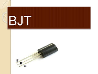
- 2. BJT Bipolar junction transistor Type of transistor that relies on the contact of two types of semiconductors for its operation. Their operation involve both electrons and holes. BJT can be used as amplifiers , switches ,temperature sensors or in oscillators. BJT can be found either as individual discrete component or in large numbers as parts of integrated circuits.
- 4. BJT AS AN ELECTRONIC SWITCH As a switch , we use the cutoff and saturation regions of BJT operation. Cutoff Region: Cutoff is easy to design. If v1<=0.5or so, the EBJ will conduct negligible current. Also, the CBJ will be reversed biased with a large Vcc. Consequently, Vo= Vcc These are the cutoff conditions and the BJT is in the “off” state. Saturation Region :Saturation is a bit more difficult to design .We need V1 sufficiently large so that the collector current becomes large enough for the CBJ to become forward biased. For the “on” state of the switch, we increase V1until the BJT saturates. This occurs when the EBJ and the CBJ are both forward biased.
- 5. BJT AS AN ELECTRONIC SWITCH When the input equals –Vin, the base-emitter junction is reverse biased or off so no current flows in the collector. When the BJT is in the cutoff, the circuit (ideally) has the following values: Vce=Vcc and Ic=0 A This state is similar to an open switch. When the input equals +Vin, the transistor is driven into saturation and the following condition occur: Vce~0V and Icsat=Vcc/Rc This state is similar to a closed switch connecting the bottom of Rc to ground.
- 6. The Characteristics for a BJT switch assumes that: 1) -Vin is low enough to drive the transistor into cutoff. 2) +Vin must produce enough base current through Rb to drive the transistor into saturation. 3) The transistor is an ideal component. These conditions can be assured by designing the circuit so that: 1) -Vin=Vbe 2) +Vin=Vbe+IbRb(Vcc is a good maximum)
- 7. Condition 1: guarantees that the circuit is driven into the cutoff region by the input. Condition 2 and 3: assures that the transistor will be driven into the saturation region.
- 9. INTRODUCTION Complementary metal–oxide– semiconductor (CMOS) is a technology for constructing integrating circuits. It is used in microcontrollers, static RAM, microprocessors and other digital logic circuits.
- 10. CMOS technology is also used for several analog circuits such as image sensors, data converters and highly integrated transceivers for many types of communication. Frank wanlass patented CMOS in 1963 .
- 11. The words "complementary- symmetry" refer to the fact that the typical digital design style with CMOS uses complementary and symmetrical pairs of p-type and n- type metal oxide semiconductor field effect transistors (MOSFETs) for logic functions.[2]
- 12. CMOS AS A SWITCH
- 13. INVERSION CMOS circuits are constructed in such a way that all PMOS transistors must have either an input from the voltage source or from another PMOS transistor. Similarly, all NMOS transistors must have either an input from ground or from another NMOS transistor