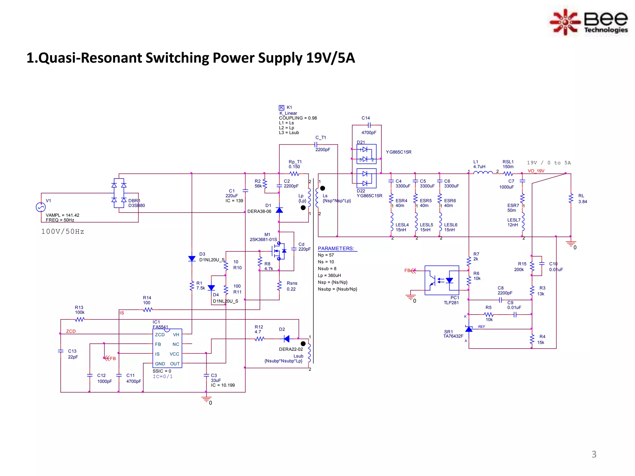
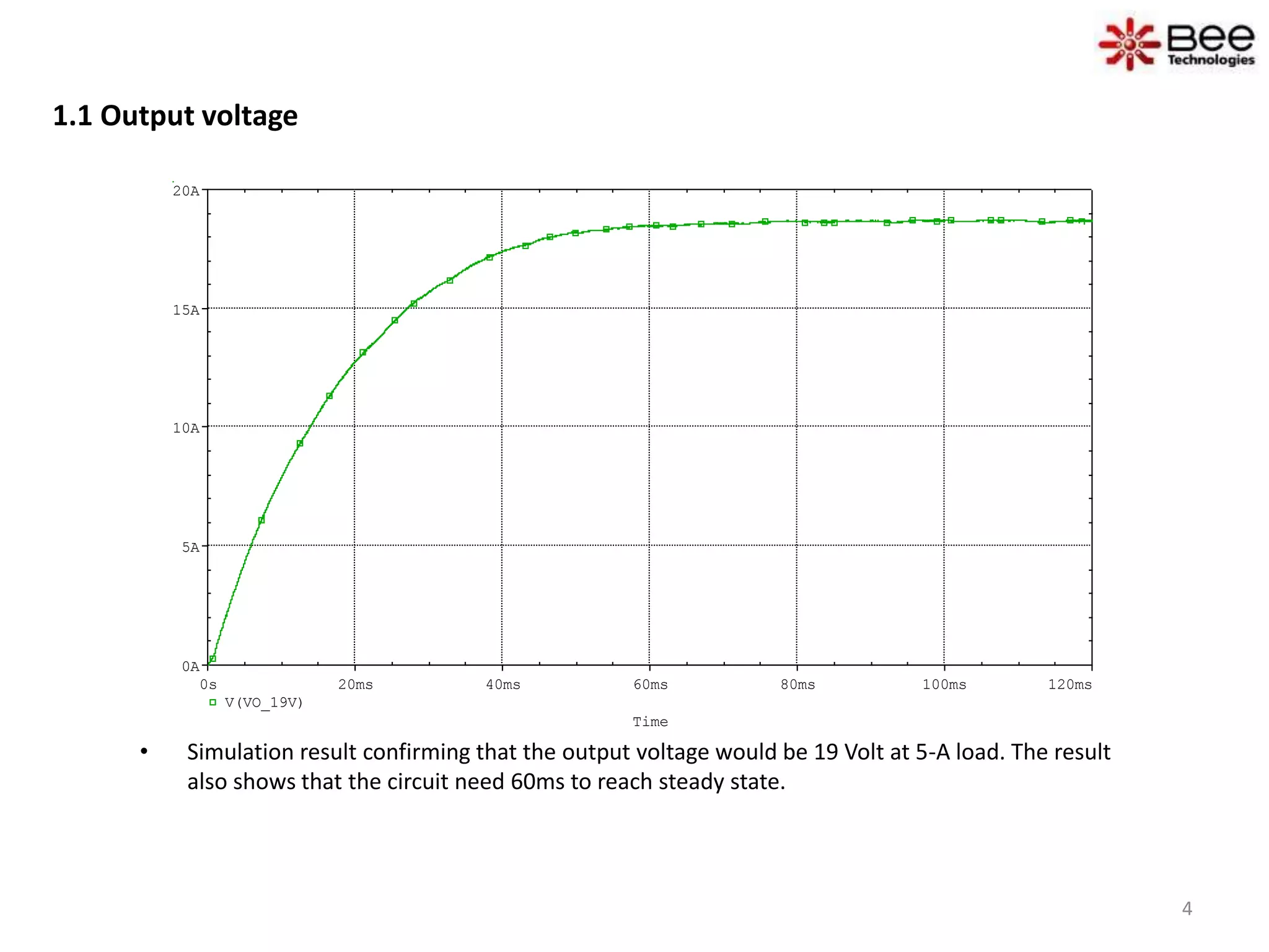
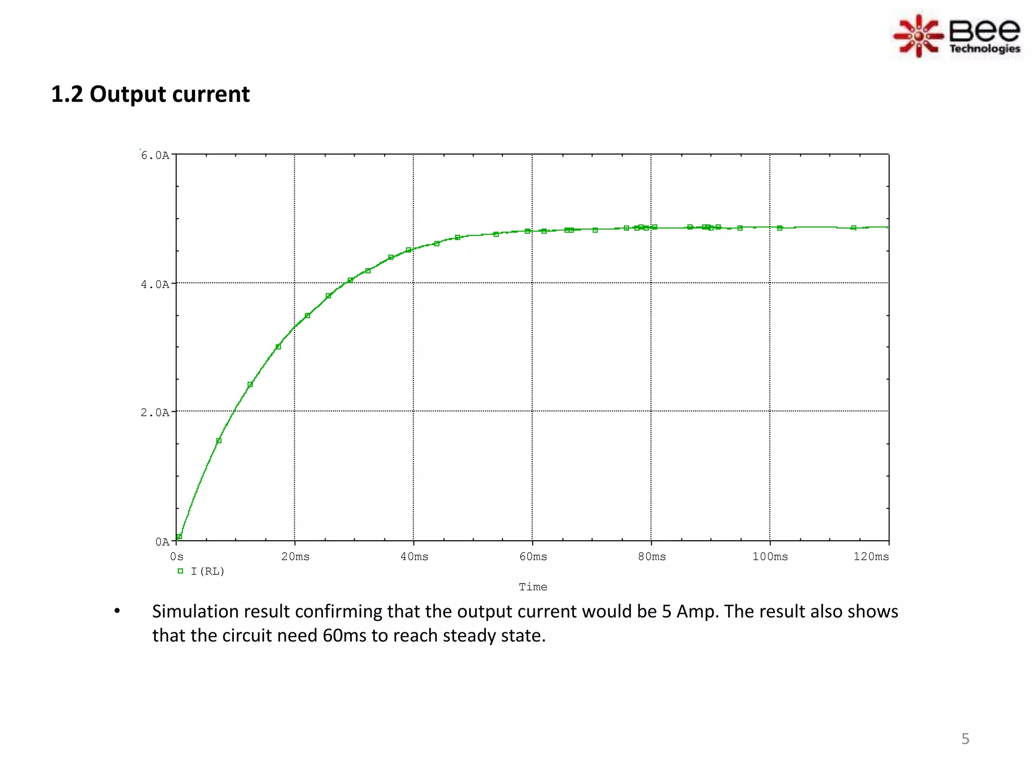
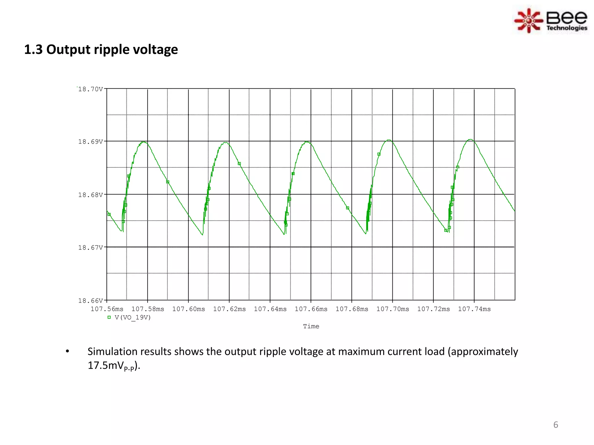
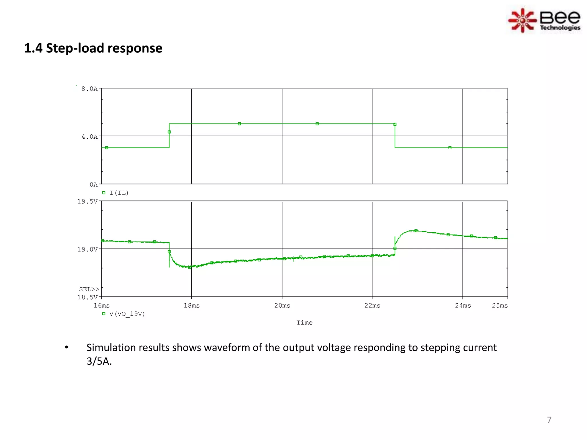
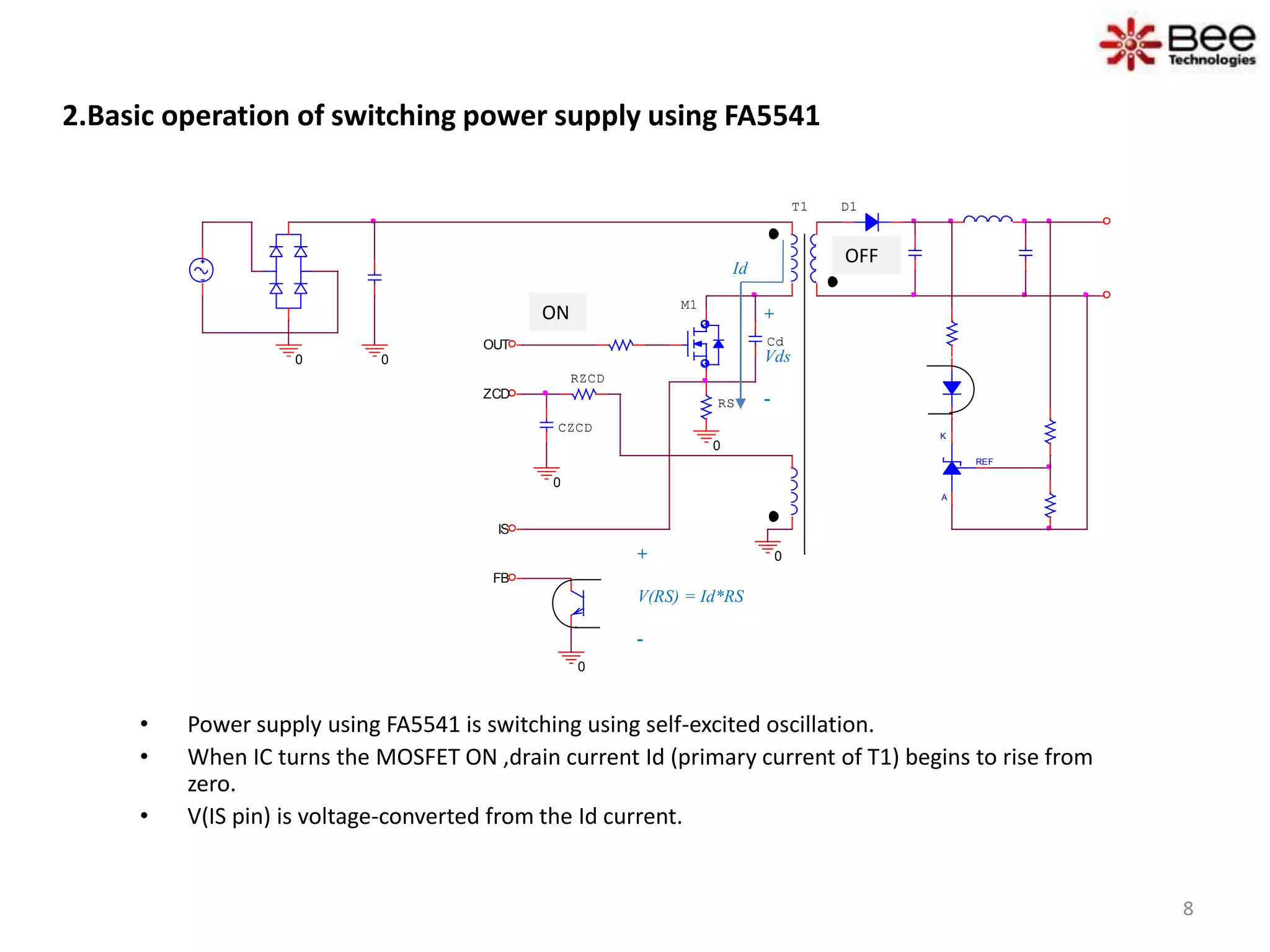
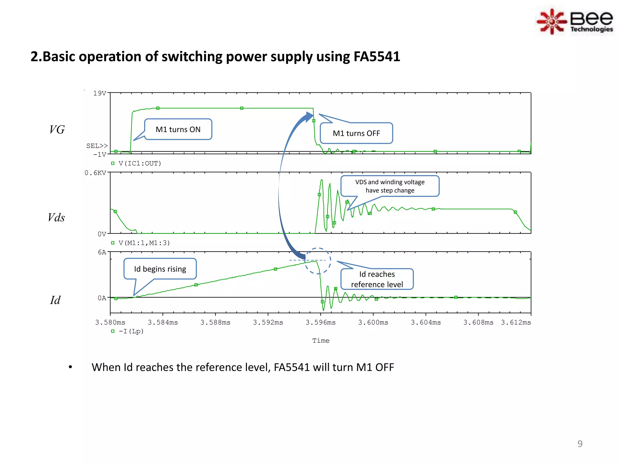
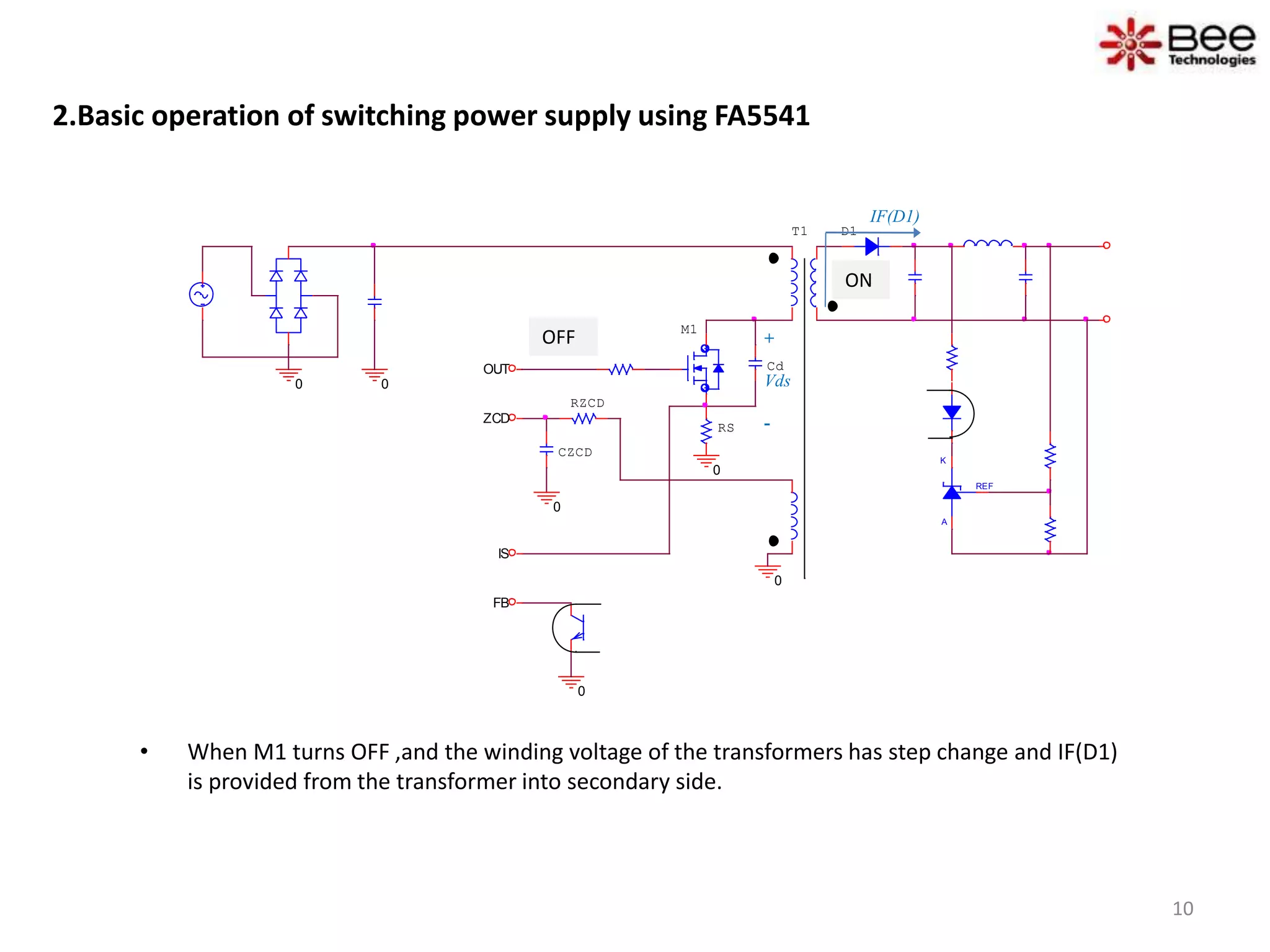
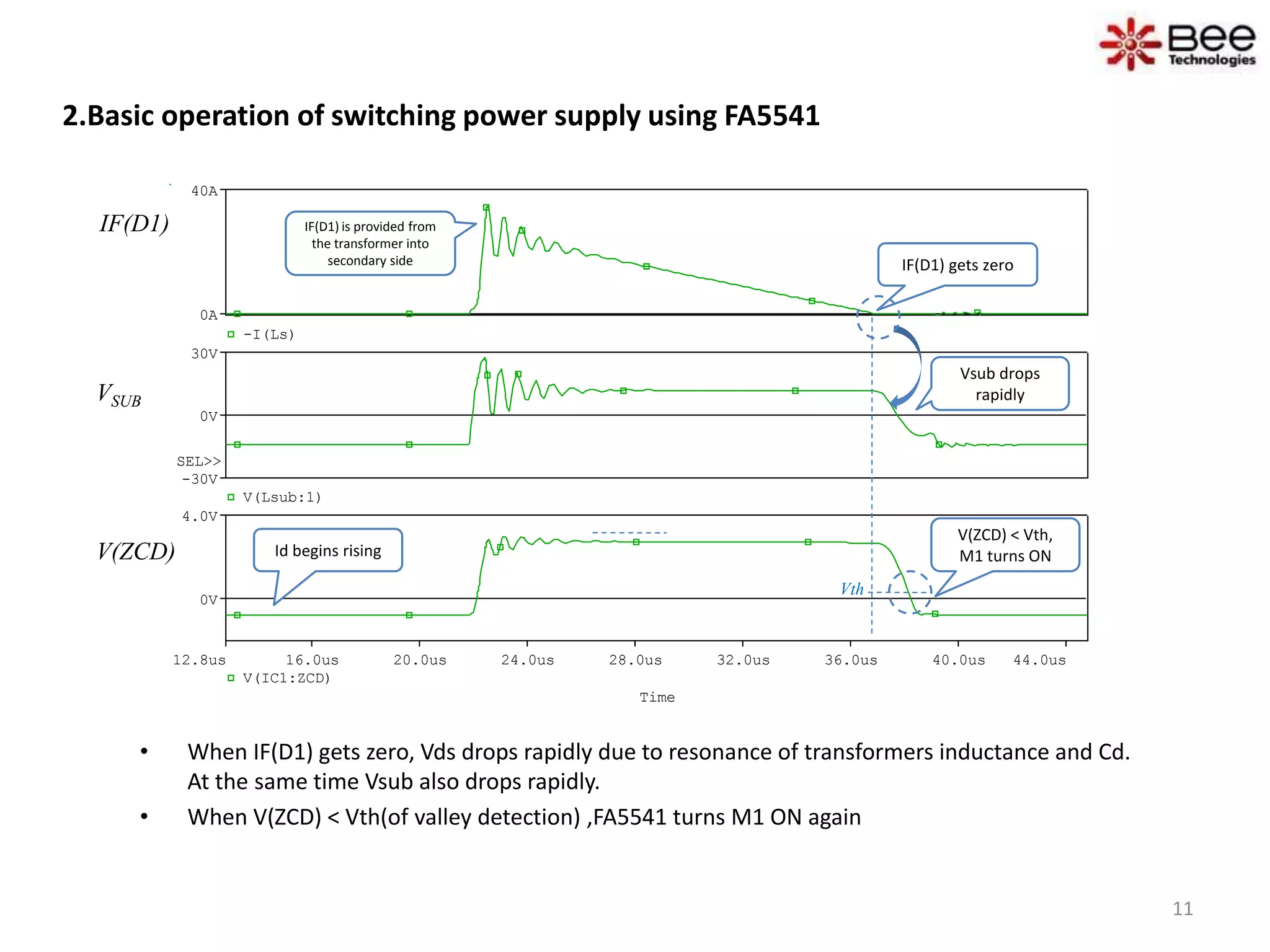
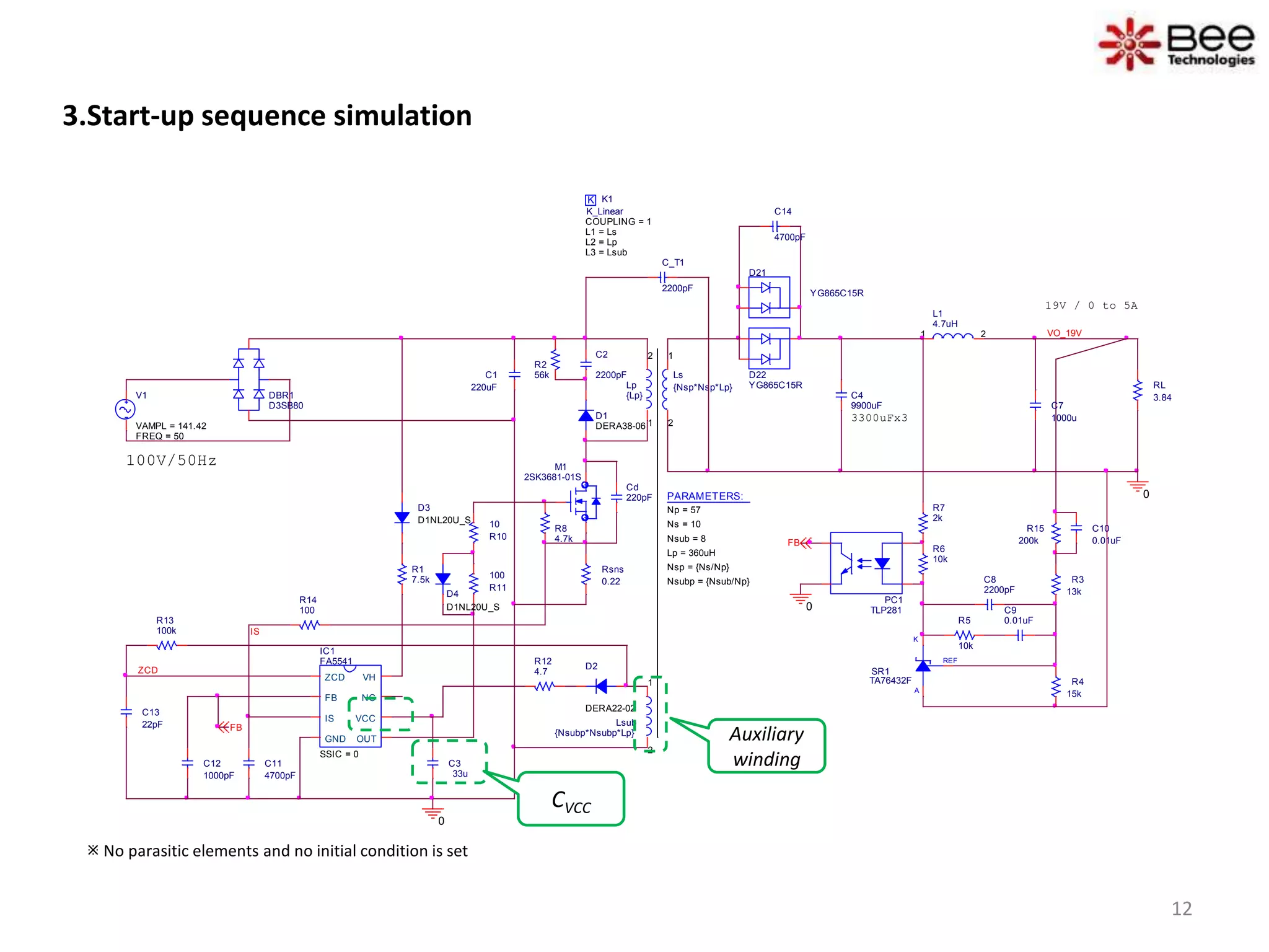
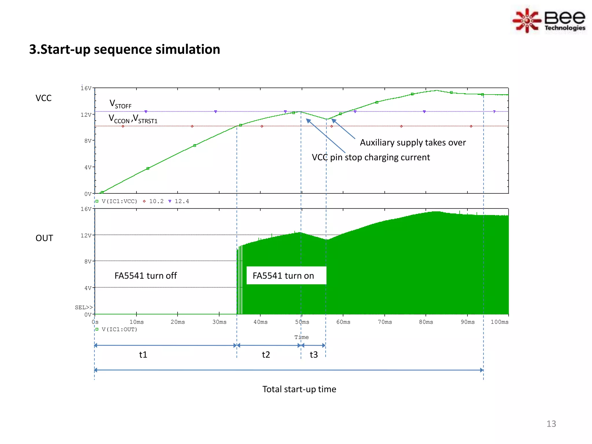
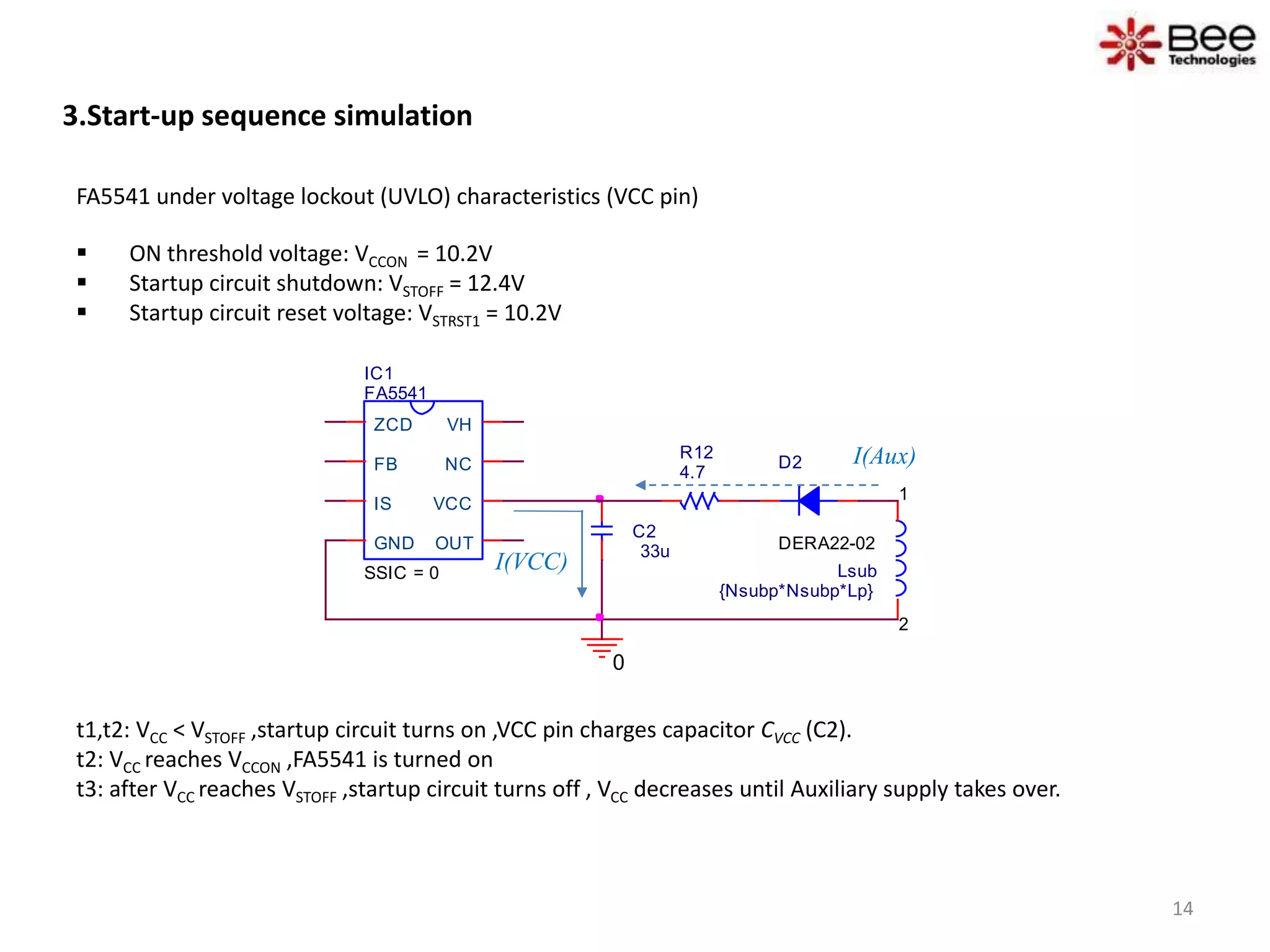
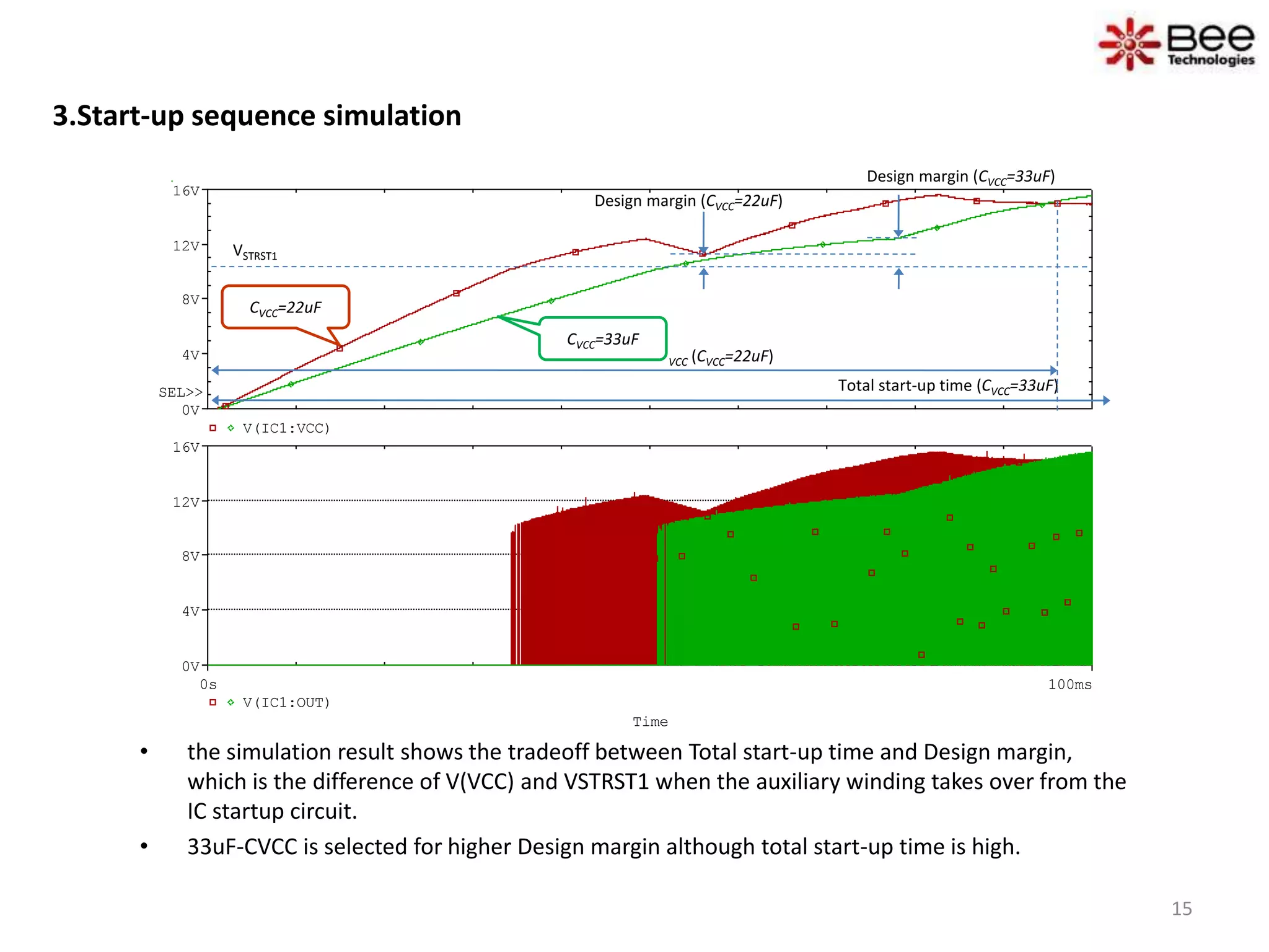
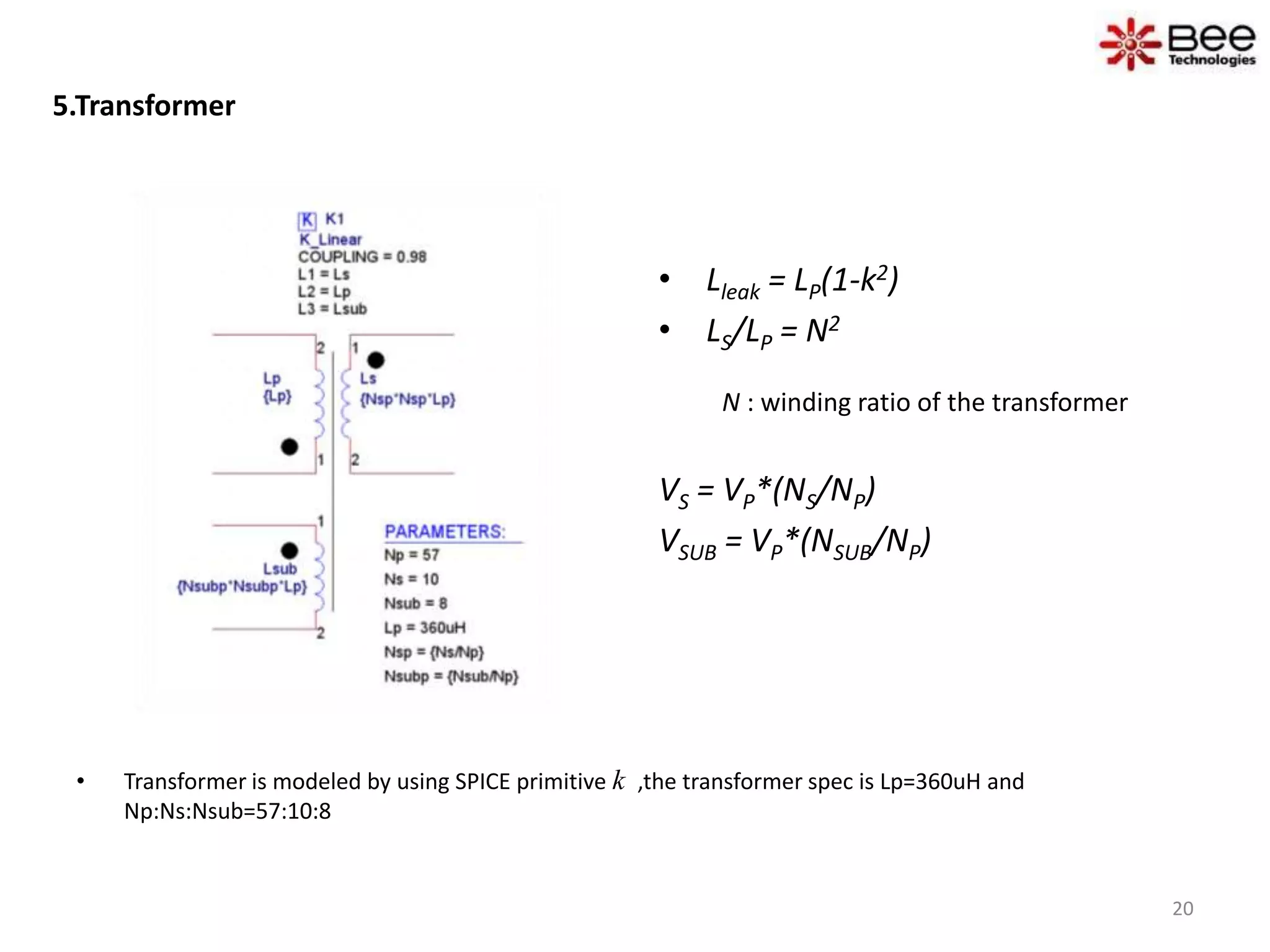
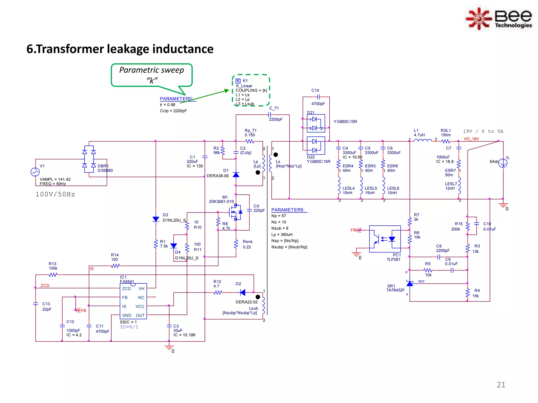
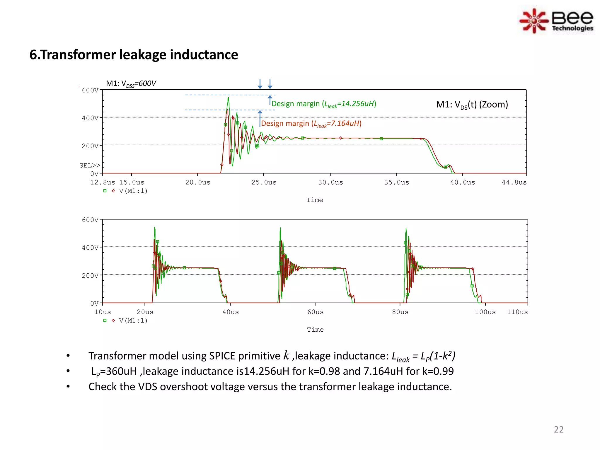
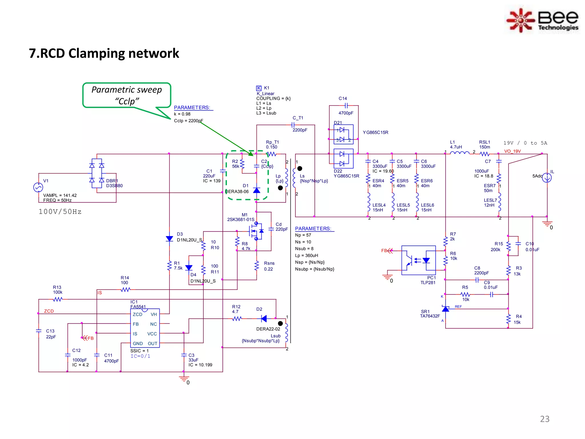
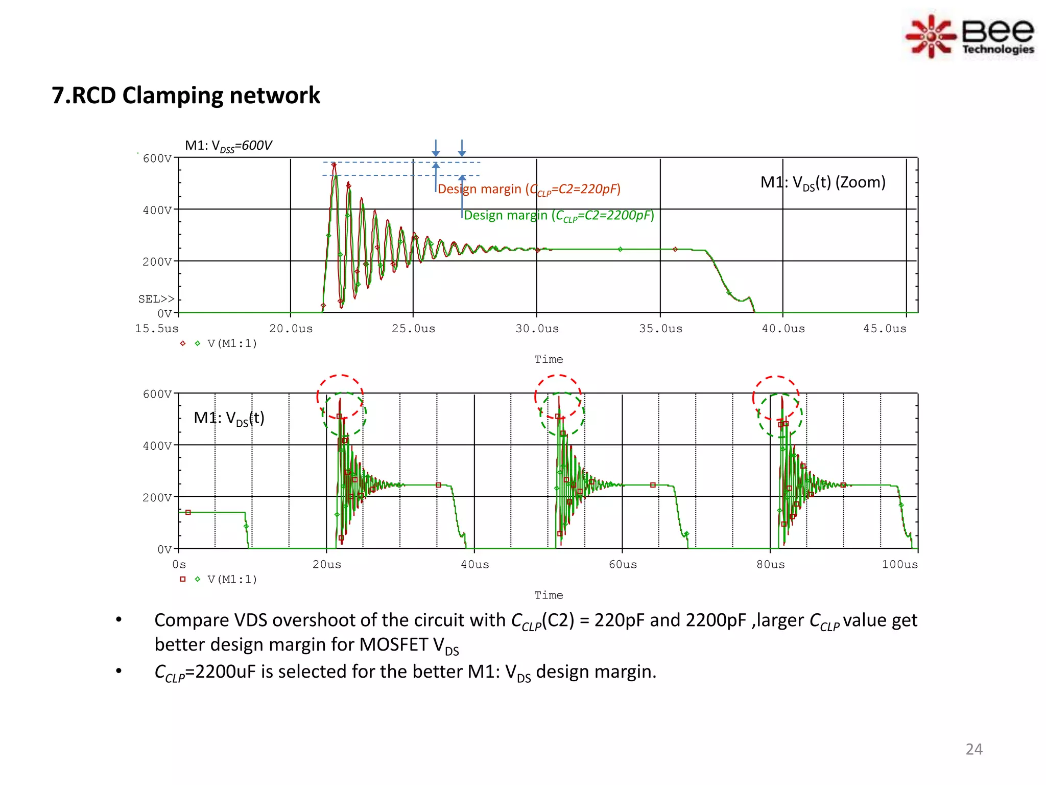
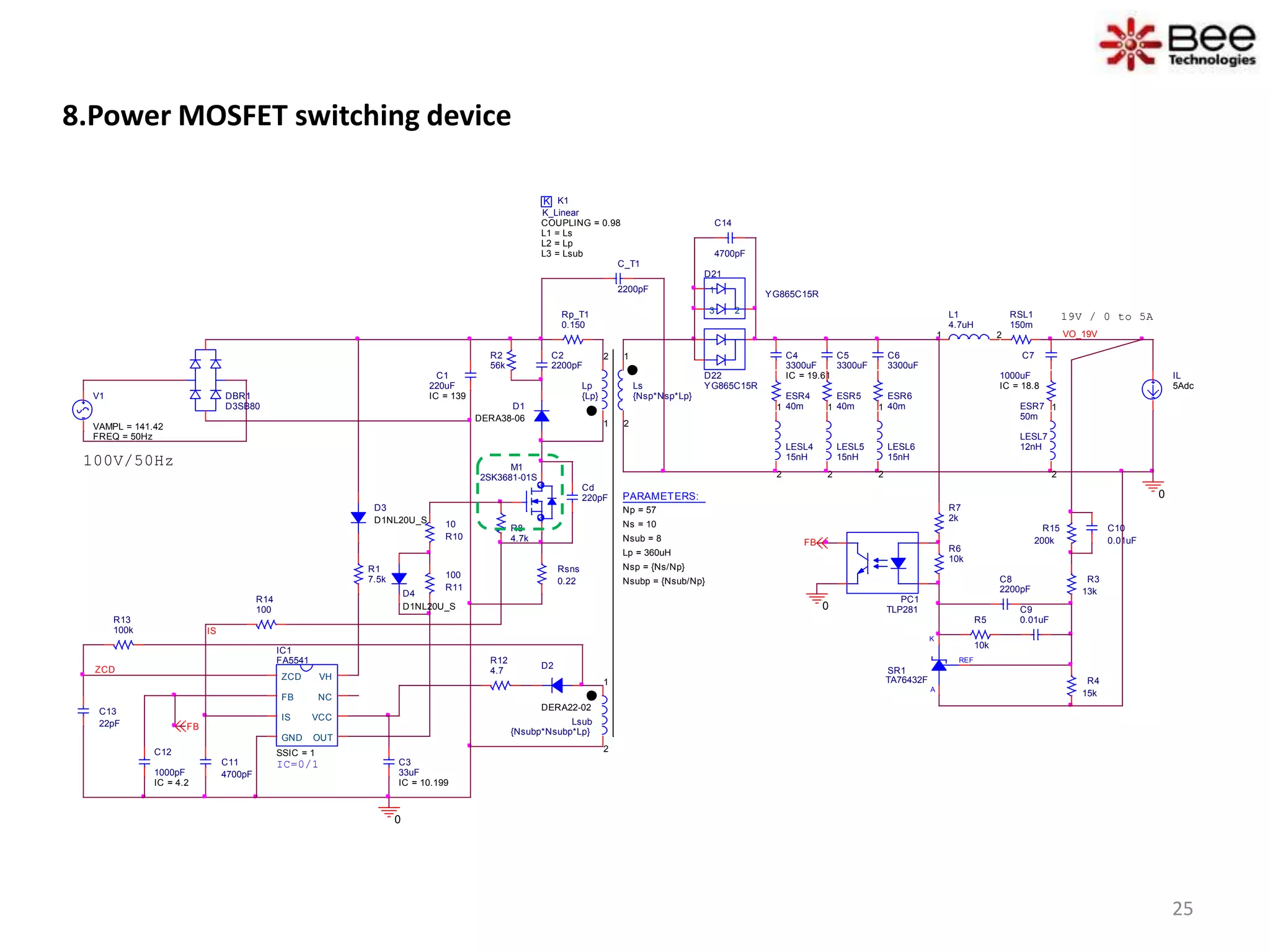
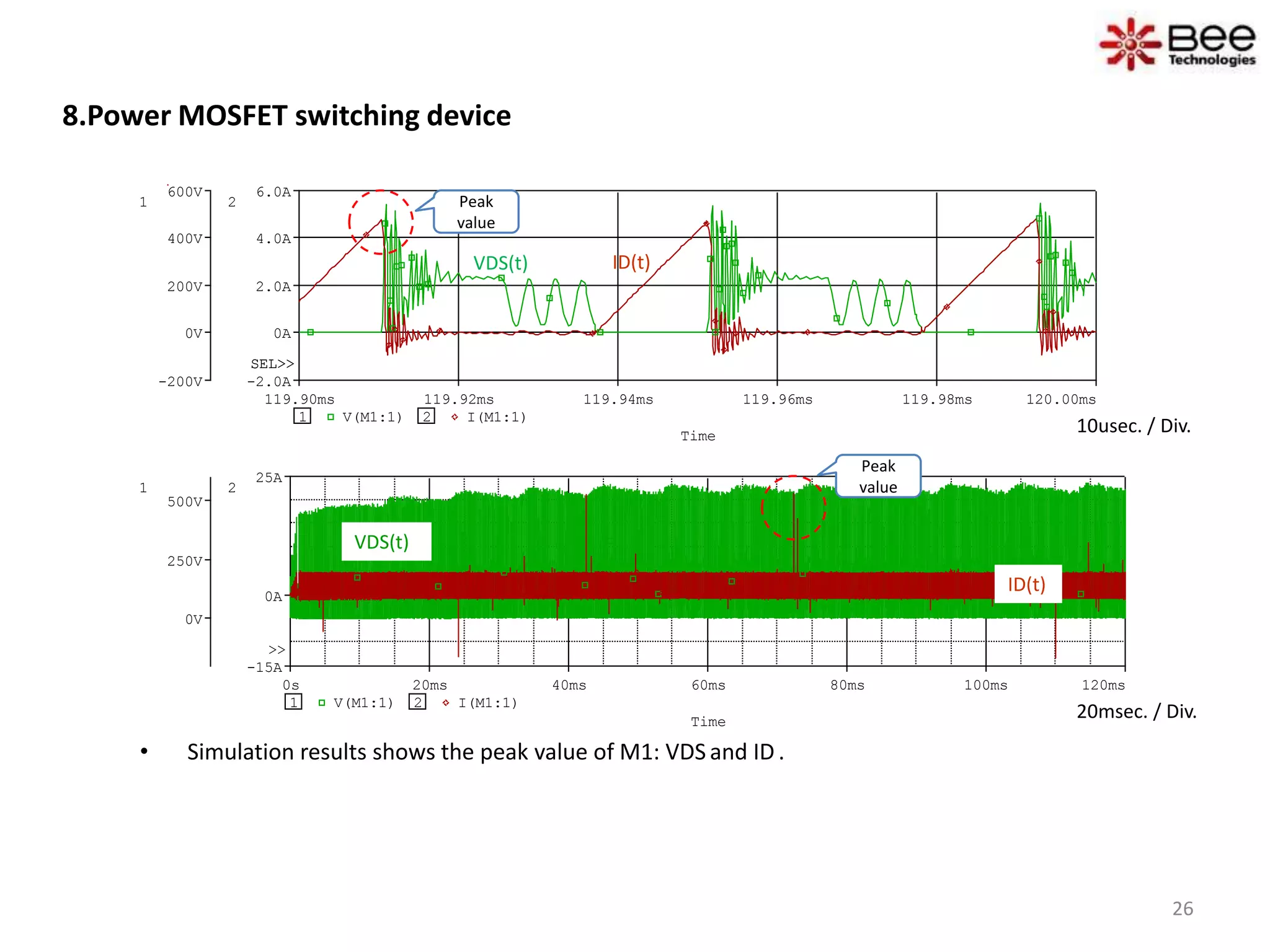
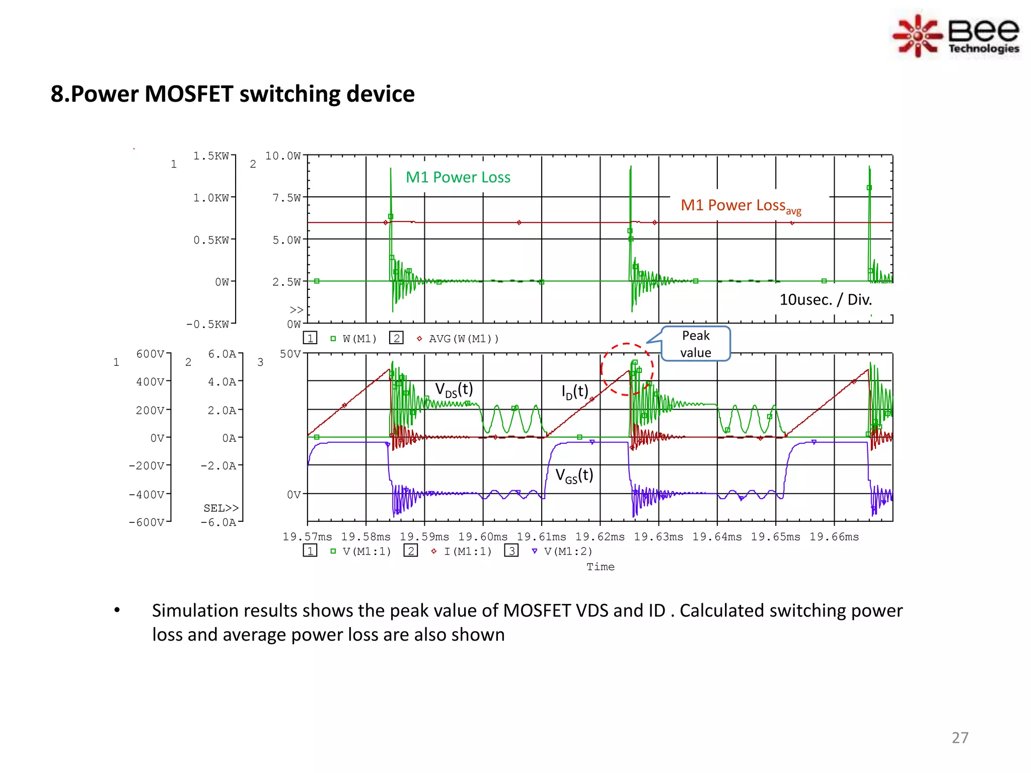
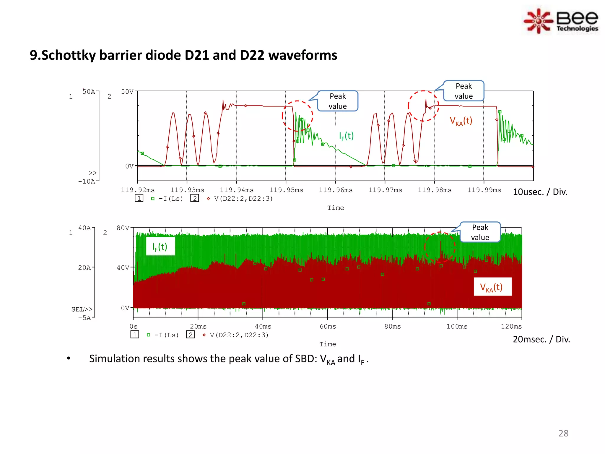
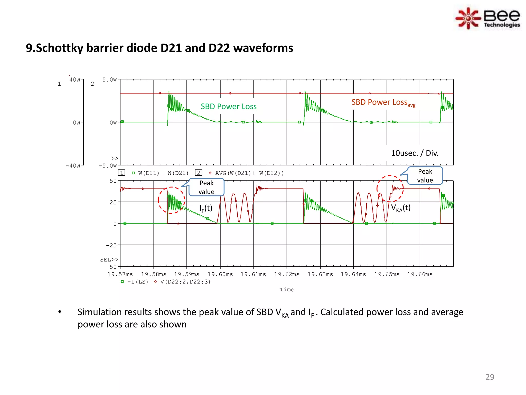
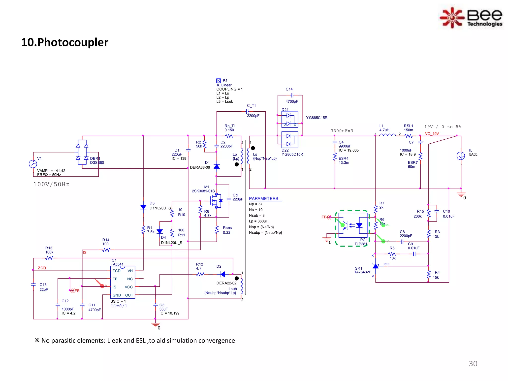
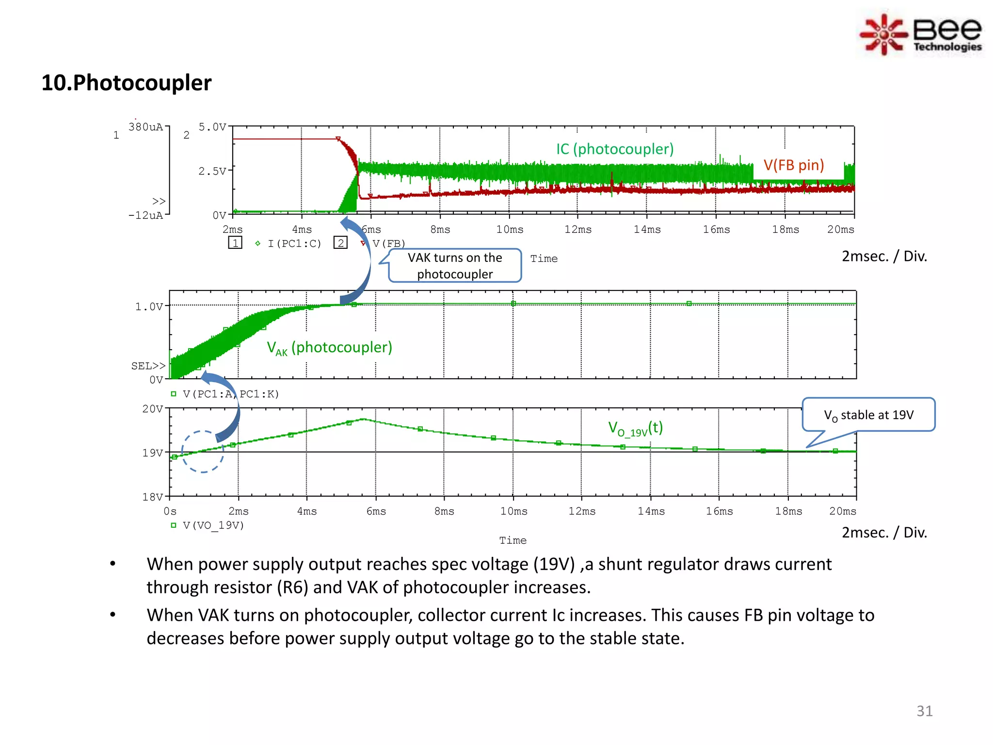
The document provides a device modeling report for a Toshiba TA7291P bridge driver IC. It includes:
- Component and part number details
- Circuit simulations and evaluation circuits showing the IC's operation under different input and output conditions
- Simulation results analyzing key parameters like supply current, input characteristics, saturation voltages, and diode characteristics.
The report concludes with 11 sections summarizing the IC's electrical behavior and performance based on circuit simulations, with tables comparing simulated and measured values.
The document discusses a simulation of a quasi-resonant switching power supply using an FA5541 controller chip. The simulation results show:
1) The output voltage is regulated at 19V with a maximum current of 5A and an output ripple voltage of approximately 17.5mVP-P.
2) Waveforms of the output responding properly to a step change in load from 3A to 5A.
3) The start-up sequence, showing the controller turning on after the voltage on the VCC pin charges and the auxiliary winding takes over once VCC reaches its threshold.
Original Transition-Mode PFC Controller IC LD7591GS 7591 SOP-8 New LeadtrendAUTHELECTRONIC
This document provides information about the LD7591 transition-mode PFC controller, including:
- It is a voltage mode PFC controller that operates in transition mode with protections like OVP, OCP, and brown-in protection.
- It has features like low startup current, over voltage protection, open feedback protection, disable function, and integrated current sensing.
- Typical applications include adapters over 65W, open frame switching power supplies, LCD TV power supplies, and LED power supplies.
SPICE MODEL of 2SJ618 (Professional+BDP Model) in SPICE PARKTsuyoshi Horigome
This document provides a summary of simulation results for a TOSHIBA 2SJ618 power MOSFET model and associated diode models from Bee Technologies. It includes characteristics such as drain current, transconductance, gate charge, switching time, output, and reverse recovery characteristics obtained from circuit simulations in comparison to measurement data with less than 3% error reported.
SPICE MODEL of 2SJ618 (Standard+BDS Model) in SPICE PARKTsuyoshi Horigome
SPICE MODEL of 2SJ618 (Standard+BDS) in SPICE PARK. English Version is http://www.spicepark.net. Japanese Version is http://www.spicepark.com by Bee Technologies.
This document provides a model evaluation report for a Texas Instruments TL431 voltage regulator component. It includes the model parameters, SPICE simulation results comparing measured and simulated component characteristics, and evaluation circuits used for testing. Simulation results match measurements well with less than 10% error for most output and reference characteristics.
SPICE MODEL of TPCA8105 (Professional+BDP Model) in SPICE PARKTsuyoshi Horigome
SPICE MODEL of TPCA8105 (Professional+BDP Model) in SPICE PARK. English Version is http://www.spicepark.net. Japanese Version is http://www.spicepark.com by Bee Technologies.
SPICE MODEL of TK65E10N1 (Standard+BDS Model) in SPICE PARKTsuyoshi Horigome
This document provides a 14-page report on modeling and simulation parameters for a Toshiba MOSFET transistor (TK65E10N1). It includes:
- MOSFET model parameters for the PSpice simulation.
- Simulation results and comparisons to measurements for various transistor characteristics like transconductance, output characteristics, capacitance, gate charge, switching times and reverse recovery.
- Circuit schematics used to simulate and evaluate the transistor parameters.
- Tables and graphs comparing simulation results to manufacturer measurements with good agreement within a few percent error.
SPICE MODEL of TK65E10N1 (Professional+BDP Model) in SPICE PARKTsuyoshi Horigome
This document provides a summary of simulation results for the electrical characteristics of a Toshiba TK65E10N1 MOSFET device, including:
- Transconductance characteristics showing less than 1% error between measured and simulated values.
- Vgs-Id, output, and Rds(on) characteristics with errors under 2%.
- Gate charge, switching time, and body diode characteristics within 2% of measurements.
- Reverse recovery characteristics of the body diode matching measurements to within 0.5% error.
SPICE MODEL of TPCC8105 (Standard+BDS Model) in SPICE PARKTsuyoshi Horigome
SPICE MODEL of TPCC8105 (Standard+BDS) in SPICE PARK. English Version is http://www.spicepark.net. Japanese Version is http://www.spicepark.com by Bee Technologies.
SPICE MODEL of TPCA8105 (Standard+BDS Model) in SPICE PARKTsuyoshi Horigome
SPICE MODEL of TPCA8105 (Standard+BDS) in SPICE PARK. English Version is http://www.spicepark.net. Japanese Version is http://www.spicepark.com by Bee Technologies.
Original Power Factor Correction IC UCC28061DR 28061 SOP-16 New Texas Instrum...AUTHELECTRONIC
The UCC28061 is a transition-mode PFC controller that features natural interleaving to improve efficiency and reduce component size. It provides complete system-level protections including input brownout, output overvoltage, and thermal shutdown. The device utilizes a natural interleaving technique where both channels operate as masters synchronized to the same frequency, delivering strong matching and fast response.
Original IGBT N-Channel FGA25N120 25N120 ANTD 25A 1200V Newauthelectroniccom
This document provides information on the FGA25N120ANTD 1200V, 25A NPT trench IGBT from Fairchild Semiconductor Corporation. It has the following key specifications:
- Low saturation voltage of 2.0V at 25A collector current and 25°C case temperature.
- Low switching losses of 0.96mJ turn-off switching loss at 25A collector current and 25°C case temperature.
- Enhanced avalanche capability making it suitable for resonant or soft switching applications such as induction heating and microwave ovens.
- Packaged in a TO-3P package and has maximum ratings of 1200V collector-emitter voltage and 50A collector current at
SPICE MODEL of TPCC8105 (Professional+BDP Model) in SPICE PARKTsuyoshi Horigome
SPICE MODEL of TPCC8105 (Professional+BDP Model) in SPICE PARK. English Version is http://www.spicepark.net. Japanese Version is http://www.spicepark.com by Bee Technologies.
SPICE MODEL of TPCA8057-H (Professional+BDP Model) in SPICE PARKTsuyoshi Horigome
SPICE MODEL of TPCA8057-H (Professional+BDP Model) in SPICE PARK. English Version is http://www.spicepark.net. Japanese Version is http://www.spicepark.com by Bee Technologies.
Original NPN Transistor 2SC3852A C3852A 3852 TO-220F New SankenAUTHELECTRONIC
This document provides specifications and characteristics for the 2SC3852/3852A NPN epitaxial planar transistor. It includes:
1) Typical IC-VCE, hFE-IC, and other characteristics curves showing parameters like current gain and saturation voltage at different currents and temperatures.
2) Maximum ratings for voltages, currents, power dissipation, and storage temperature.
3) Electrical characteristic specifications for current, voltage, gain, and switching performance under given conditions.
4) The transistor's external dimensions and packaging in a TO-220F case.
The document compares the performance of a MOSFET model in PSpice and LTspice simulation software. It includes circuits and characteristic graphs for the MOSFET's ID-VGS, output, Rds(on), switching time, and gate charge characteristics. The summaries show the characteristics are similar between the two simulations, but PSpice provides more accurate results.
This document summarizes the simulation results of an operational amplifier component (NJM2068M) for key parameters including output voltage swing, input offset voltage, slew rate, input current, open loop voltage gain, and common mode rejection ratio. The simulation results are compared to the datasheet specifications and percent errors are reported to validate the accuracy of the SPICE model.
The MIC38HC42/3/4/5 are current-mode PWM controllers with 1A drive capability and operating voltage ranges of 14.5V to 9V and 8.4V to 7.6V. They have low start-up and operating currents compared to similar bipolar controllers, and feature fast switching times, rail-to-rail output, and pin compatibility with existing controllers. They are suitable for use in applications such as switched-mode power supplies, DC-DC converters, and other power regulation circuits where high efficiency is required.
Original Gate Driver IC TD62083APG 62083APG 62083 DIP-18 New ToshibaAUTHELECTRONIC
This document provides specifications for the TD62083APG/AFG and TD62084APG/AFG integrated circuits from Toshiba. They are 8-channel Darlington sink drivers comprised of NPN Darlington pairs, with each channel capable of 500mA of output current. Key features include integral clamp diodes, compatible inputs for various logic types, DIP-18 and SOP-18 packaging options. Electrical characteristics, test circuits, precautions and package dimensions are provided.
This document provides data sheets for several quad operational amplifier integrated circuits, including the CA124, CA224, CA324, LM324, and LM2902. It summarizes their key specifications such as operating temperature range, voltage gain, bandwidth, input/output voltage ranges, power requirements, and packaging options. The amplifiers each contain four independent high-gain op-amps on a single chip and are designed for use in commercial, industrial and military applications requiring operation from single or dual power supplies.
The document provides information on the LM555 timer integrated circuit. It can be used to generate accurate time delays or oscillations. In monostable mode, the time is controlled by one external resistor and capacitor. In astable mode, frequency and duty cycle are controlled by two resistors and one capacitor. It has applications in precision timing, pulse generation, and more. Key specifications and electrical characteristics are provided.
The document provides information on the LM555 timer integrated circuit. It can be used to generate precise time delays or oscillations. In monostable mode, the time is controlled by a single external resistor and capacitor. In astable mode, frequency and duty cycle are set by two resistors and a capacitor. It has applications in timing, pulse generation, and more. Key specifications include timing accuracy better than 0.5% and an output that can source or sink up to 200mA.
The document provides design details for a critical conduction mode power factor correction (PFC) circuit. It includes:
1) An introduction describing the need for power factor correction to draw sinusoidal current in phase with input voltage for improved power factor.
2) An application circuit diagram for a 400V/200W PFC circuit using a TB6819AFG controller IC along with component values and simulation parameters.
3) Explanations of techniques used including time scaling to speed up simulations and modeling of a common mode choke coil.
4) An 8-step design process covering the output voltage feedback, output capacitor sizing, inductor, input capacitor, auxiliary winding, current/zero current detection
This document provides information on the TL284xB and TL384xB series of integrated circuits from Texas Instruments. The ICs provide features for implementing current-mode control schemes for offline or DC-DC power supplies with minimum external components. Key features include undervoltage lockout, precision reference, latching PWM for current limiting, and a high-current totem-pole output. The document describes the package options and ordering information for the various models in the series.
This document provides information about the TLV3491, TLV3492, and TLV3494 push-pull output comparators. Key details include:
- They feature a fast 6μs response time and low power capability of <1.2μA operating from 1.8V to 5.5V.
- Input common-mode range extends beyond the supply rails, making them suitable for low-voltage applications.
- They are available in small packages like SOT23 and SOIC suitable for portable and space-constrained applications.
- Applications include portable medical equipment, wireless security systems, remote controls, and other low power systems.
The document describes the UCC3895 BiCMOS advanced phase-shift PWM controller. It has features such as programmable output turn-on delay, adaptive delay set, bidirectional oscillator synchronization, and voltage-mode or current-mode control. It can operate at frequencies up to 1 MHz with typical operating current of 5 mA at 500 kHz. The UCC3895 is a phase-shift PWM controller that implements full-bridge power stage control by phase shifting one half-bridge with respect to the other, allowing constant frequency pulse-width modulation with zero-voltage switching for high efficiency at high frequencies. It improves on previous controller families with additional features such as enhanced control logic and adaptive delay set.
The STR-X6759N is a quasi-resonant topology integrated circuit designed for SMPS applications. It provides low EMI noise characteristics through its quasi-resonant topology and soft switching of the internal MOSFET. It also features a bottom-skip mode to improve efficiency over the load range and a standby mode to reduce input power at light loads. Protections such as overvoltage, overload, and overcurrent protections improve reliability.
This document provides information on the UC3844, UC3845, UC2844, and UC2845 high performance current mode controllers, including:
- Operating temperature ranges and packaging for the devices.
- Pin connections and ordering information for the different package types.
- Electrical characteristics like reference voltage, oscillator frequency, error amplifier performance, current sense input, output specifications, and undervoltage lockout thresholds.
- Graphs depicting properties like oscillator frequency vs timing resistor, output deadtime vs frequency, error amplifier gain and phase vs frequency, and more.
- An overview of key features like current mode operation, adjustable output deadtime, compensation, current limiting, undervoltage lockout,
The NCP1032 is an integrated circuit that can be used to implement switching regulator applications with minimal external components. It contains all the active power control logic and protection circuitry needed, including an on-chip high voltage power switch, startup circuit, fixed frequency oscillator up to 1 MHz, and current limit, soft start, and thermal protection features. It is well-suited for applications requiring up to 3W output in isolated power supplies for telecom and medical equipment.
This document provides information on the MJE13003 NPN silicon transistor from Unisonic Technologies Co., Ltd. It describes the transistor as being designed for high-voltage, high-speed power switching in inductive circuits. Key features include a reverse biased safe operating area with inductive loads up to 1.5 amps and a typical fall time of 290ns at 1 amp and 100°C. The transistor has applications in switching regulators, inverters, motor controls, solenoid drivers, and deflection circuits. Electrical characteristics and maximum ratings are provided in tables and graphs.
This document provides information on optocouplers (IL4116/IL4117/IL4118) that have a phototriac output, zero crossing detection, and very low input current. The optocouplers consist of an LED optically coupled to a photosensitive zero crossing TRIAC network and can isolate low voltage logic from 120/240/380VAC lines. They feature high input sensitivity down to 1.3mA, zero voltage crossing operation, blocking voltages up to 800V, and on-state currents up to 300mA. The optocouplers can control loads such as motors, solenoids, thyristors and relays in applications including solid state relays,
The document provides design details for a critical conduction mode power factor correction (PFC) circuit using the TB6819AFG controller IC. It includes the application circuit, design specifications, equations for determining component values like the output inductor L1, input capacitor C1, and output capacitor C2. It also describes the use of time scaling to speed up transient simulations and modeling of the common mode choke coil. The steps outlined include selecting the output voltage and feedback circuit, output capacitor, inductance L1, input capacitor C4, auxiliary winding L2, and circuits for current detection and zero current detection.
This document provides information about the L298 dual full-bridge driver integrated circuit. It can drive loads such as relays, solenoids, and DC/stepping motors with a maximum current of 4A and voltage up to 46V. It has two bridges that can each drive an inductive load independently based on input signals. The circuit has overtemperature protection and logic-level inputs with noise immunity.
Original Opto PC957L PC957 P957 957 DIP-8 New Sharpauthelectroniccom
This document provides specifications for the PC957L0NSZ0F series of photocouplers. Key details include:
1. It is an 8-pin DIP or SMT package photocoupler with input-output isolation of 5.0kVrms, high-speed response up to 1Mbps, and high common mode rejection ratio of 15kV/μs.
2. It has approvals from UL and VDE and is lead-free and RoHS compliant. Applications include use in programmable controllers and inverters.
3. Electrical characteristics include a forward voltage of 1-1.6V, rise/fall times of 0.2/0.
This document provides information about the L298 dual full-bridge driver integrated circuit. It can drive loads such as relays, solenoids, and DC/stepper motors with a maximum current of 4A and voltage up to 46V. It has two bridges that can each drive an inductive load independently based on input signals. The circuit has overtemperature protection and logic inputs that are TTL compatible with noise immunity. Pinouts, electrical specifications, application examples, and dimensions are provided.
This document summarizes the NE555, SA555, and SE555 monolithic timing circuits. It provides:
1) Pin connections, electrical characteristics including timing accuracy, input/output voltage levels, and operating conditions.
2) Descriptions and schematics for operating the NE555 in monostable (one-shot) and astable (oscillator) modes using external resistors and capacitors to control timing.
3) Examples of applications including pulse width modulation, linear ramp generation, and a 50% duty cycle oscillator. Tables, figures and waveforms illustrate the timer's operation and specifications.
Similar to シミュレーション事例:擬似共振電源回路シミュレーション Quasi-Resonant Switching Power Supply using FA5541 (20)
Comparative analysis between traditional aquaponics and reconstructed aquapon...bijceesjournal
The aquaponic system of planting is a method that does not require soil usage. It is a method that only needs water, fish, lava rocks (a substitute for soil), and plants. Aquaponic systems are sustainable and environmentally friendly. Its use not only helps to plant in small spaces but also helps reduce artificial chemical use and minimizes excess water use, as aquaponics consumes 90% less water than soil-based gardening. The study applied a descriptive and experimental design to assess and compare conventional and reconstructed aquaponic methods for reproducing tomatoes. The researchers created an observation checklist to determine the significant factors of the study. The study aims to determine the significant difference between traditional aquaponics and reconstructed aquaponics systems propagating tomatoes in terms of height, weight, girth, and number of fruits. The reconstructed aquaponics system’s higher growth yield results in a much more nourished crop than the traditional aquaponics system. It is superior in its number of fruits, height, weight, and girth measurement. Moreover, the reconstructed aquaponics system is proven to eliminate all the hindrances present in the traditional aquaponics system, which are overcrowding of fish, algae growth, pest problems, contaminated water, and dead fish.
Use PyCharm for remote debugging of WSL on a Windo cf5c162d672e4e58b4dde5d797...shadow0702a
This document serves as a comprehensive step-by-step guide on how to effectively use PyCharm for remote debugging of the Windows Subsystem for Linux (WSL) on a local Windows machine. It meticulously outlines several critical steps in the process, starting with the crucial task of enabling permissions, followed by the installation and configuration of WSL.
The guide then proceeds to explain how to set up the SSH service within the WSL environment, an integral part of the process. Alongside this, it also provides detailed instructions on how to modify the inbound rules of the Windows firewall to facilitate the process, ensuring that there are no connectivity issues that could potentially hinder the debugging process.
The document further emphasizes on the importance of checking the connection between the Windows and WSL environments, providing instructions on how to ensure that the connection is optimal and ready for remote debugging.
It also offers an in-depth guide on how to configure the WSL interpreter and files within the PyCharm environment. This is essential for ensuring that the debugging process is set up correctly and that the program can be run effectively within the WSL terminal.
Additionally, the document provides guidance on how to set up breakpoints for debugging, a fundamental aspect of the debugging process which allows the developer to stop the execution of their code at certain points and inspect their program at those stages.
Finally, the document concludes by providing a link to a reference blog. This blog offers additional information and guidance on configuring the remote Python interpreter in PyCharm, providing the reader with a well-rounded understanding of the process.
Discover the latest insights on Data Driven Maintenance with our comprehensive webinar presentation. Learn about traditional maintenance challenges, the right approach to utilizing data, and the benefits of adopting a Data Driven Maintenance strategy. Explore real-world examples, industry best practices, and innovative solutions like FMECA and the D3M model. This presentation, led by expert Jules Oudmans, is essential for asset owners looking to optimize their maintenance processes and leverage digital technologies for improved efficiency and performance. Download now to stay ahead in the evolving maintenance landscape.
Rainfall intensity duration frequency curve statistical analysis and modeling...bijceesjournal
Using data from 41 years in Patna’ India’ the study’s goal is to analyze the trends of how often it rains on a weekly, seasonal, and annual basis (1981−2020). First, utilizing the intensity-duration-frequency (IDF) curve and the relationship by statistically analyzing rainfall’ the historical rainfall data set for Patna’ India’ during a 41 year period (1981−2020), was evaluated for its quality. Changes in the hydrologic cycle as a result of increased greenhouse gas emissions are expected to induce variations in the intensity, length, and frequency of precipitation events. One strategy to lessen vulnerability is to quantify probable changes and adapt to them. Techniques such as log-normal, normal, and Gumbel are used (EV-I). Distributions were created with durations of 1, 2, 3, 6, and 24 h and return times of 2, 5, 10, 25, and 100 years. There were also mathematical correlations discovered between rainfall and recurrence interval.
Findings: Based on findings, the Gumbel approach produced the highest intensity values, whereas the other approaches produced values that were close to each other. The data indicates that 461.9 mm of rain fell during the monsoon season’s 301st week. However, it was found that the 29th week had the greatest average rainfall, 92.6 mm. With 952.6 mm on average, the monsoon season saw the highest rainfall. Calculations revealed that the yearly rainfall averaged 1171.1 mm. Using Weibull’s method, the study was subsequently expanded to examine rainfall distribution at different recurrence intervals of 2, 5, 10, and 25 years. Rainfall and recurrence interval mathematical correlations were also developed. Further regression analysis revealed that short wave irrigation, wind direction, wind speed, pressure, relative humidity, and temperature all had a substantial influence on rainfall.
Originality and value: The results of the rainfall IDF curves can provide useful information to policymakers in making appropriate decisions in managing and minimizing floods in the study area.
Introduction- e - waste – definition - sources of e-waste– hazardous substances in e-waste - effects of e-waste on environment and human health- need for e-waste management– e-waste handling rules - waste minimization techniques for managing e-waste – recycling of e-waste - disposal treatment methods of e- waste – mechanism of extraction of precious metal from leaching solution-global Scenario of E-waste – E-waste in India- case studies.
Applications of artificial Intelligence in Mechanical Engineering.pdfAtif Razi
Historically, mechanical engineering has relied heavily on human expertise and empirical methods to solve complex problems. With the introduction of computer-aided design (CAD) and finite element analysis (FEA), the field took its first steps towards digitization. These tools allowed engineers to simulate and analyze mechanical systems with greater accuracy and efficiency. However, the sheer volume of data generated by modern engineering systems and the increasing complexity of these systems have necessitated more advanced analytical tools, paving the way for AI.
AI offers the capability to process vast amounts of data, identify patterns, and make predictions with a level of speed and accuracy unattainable by traditional methods. This has profound implications for mechanical engineering, enabling more efficient design processes, predictive maintenance strategies, and optimized manufacturing operations. AI-driven tools can learn from historical data, adapt to new information, and continuously improve their performance, making them invaluable in tackling the multifaceted challenges of modern mechanical engineering.
Redefining brain tumor segmentation: a cutting-edge convolutional neural netw...IJECEIAES
Medical image analysis has witnessed significant advancements with deep learning techniques. In the domain of brain tumor segmentation, the ability to
precisely delineate tumor boundaries from magnetic resonance imaging (MRI)
scans holds profound implications for diagnosis. This study presents an ensemble convolutional neural network (CNN) with transfer learning, integrating
the state-of-the-art Deeplabv3+ architecture with the ResNet18 backbone. The
model is rigorously trained and evaluated, exhibiting remarkable performance
metrics, including an impressive global accuracy of 99.286%, a high-class accuracy of 82.191%, a mean intersection over union (IoU) of 79.900%, a weighted
IoU of 98.620%, and a Boundary F1 (BF) score of 83.303%. Notably, a detailed comparative analysis with existing methods showcases the superiority of
our proposed model. These findings underscore the model’s competence in precise brain tumor localization, underscoring its potential to revolutionize medical
image analysis and enhance healthcare outcomes. This research paves the way
for future exploration and optimization of advanced CNN models in medical
imaging, emphasizing addressing false positives and resource efficiency.
Electric vehicle and photovoltaic advanced roles in enhancing the financial p...IJECEIAES
Climate change's impact on the planet forced the United Nations and governments to promote green energies and electric transportation. The deployments of photovoltaic (PV) and electric vehicle (EV) systems gained stronger momentum due to their numerous advantages over fossil fuel types. The advantages go beyond sustainability to reach financial support and stability. The work in this paper introduces the hybrid system between PV and EV to support industrial and commercial plants. This paper covers the theoretical framework of the proposed hybrid system including the required equation to complete the cost analysis when PV and EV are present. In addition, the proposed design diagram which sets the priorities and requirements of the system is presented. The proposed approach allows setup to advance their power stability, especially during power outages. The presented information supports researchers and plant owners to complete the necessary analysis while promoting the deployment of clean energy. The result of a case study that represents a dairy milk farmer supports the theoretical works and highlights its advanced benefits to existing plants. The short return on investment of the proposed approach supports the paper's novelty approach for the sustainable electrical system. In addition, the proposed system allows for an isolated power setup without the need for a transmission line which enhances the safety of the electrical network
4. 1.1 Output voltage
• Simulation result confirming that the output voltage would be 19 Volt at 5-A load. The result
also shows that the circuit need 60ms to reach steady state.
Time
0s 20ms 40ms 60ms 80ms 100ms 120ms
V(VO_19V)
0A
5A
10A
15A
20A
4
5. 1.2 Output current
• Simulation result confirming that the output current would be 5 Amp. The result also shows
that the circuit need 60ms to reach steady state.
Time
0s 20ms 40ms 60ms 80ms 100ms 120ms
I(RL)
0A
2.0A
4.0A
6.0A
5
6. • Simulation results shows the output ripple voltage at maximum current load (approximately
17.5mVP-P).
Time
107.56ms 107.58ms 107.60ms 107.62ms 107.64ms 107.66ms 107.68ms 107.70ms 107.72ms 107.74ms
V(VO_19V)
18.66V
18.67V
18.68V
18.69V
18.70V
1.3 Output ripple voltage
6
7. 1.4 Step-load response
• Simulation results shows waveform of the output voltage responding to stepping current
3/5A.
Time
16ms 18ms 20ms 22ms 24ms 25ms
V(VO_19V)
19.0V
18.5V
19.5V
SEL>>
I(IL)
0A
4.0A
8.0A
7
8. 2.Basic operation of switching power supply using FA5541
• Power supply using FA5541 is switching using self-excited oscillation.
• When IC turns the MOSFET ON ,drain current Id (primary current of T1) begins to rise from
zero.
• V(IS pin) is voltage-converted from the Id current.
REF
K
A
0
0
0
OUT
ZCD
IS
FB
RZCD
CZCD
RS
0
M1
Cd
D1T1
0
0
+
Vds
-
ON
Id
+
V(RS) = Id*RS
-
OFF
8
9. 2.Basic operation of switching power supply using FA5541
Time
3.580ms 3.584ms 3.588ms 3.592ms 3.596ms 3.600ms 3.604ms 3.608ms 3.612ms
-I(Lp)
0A
6A
V(M1:1,M1:3)
0V
0.6KV
V(IC1:OUT)
-1V
19V
SEL>>
• When Id reaches the reference level, FA5541 will turn M1 OFF
Id
Vds
VG
Id begins rising
M1 turns ON
Id reaches
reference level
M1 turns OFF
VDS and winding voltage
have step change
9
10. REF
K
A
0
0
0
OUT
ZCD
IS
FB
RZCD
CZCD
RS
0
M1
Cd
D1T1
0
0
• When M1 turns OFF ,and the winding voltage of the transformers has step change and IF(D1)
is provided from the transformer into secondary side.
+
Vds
-
OFF
IF(D1)
ON
2.Basic operation of switching power supply using FA5541
10
11. 2.Basic operation of switching power supply using FA5541
Time
16.0us 20.0us 24.0us 28.0us 32.0us 36.0us 40.0us 44.0us12.8us
V(IC1:ZCD)
0V
4.0V
V(Lsub:1)
0V
-30V
30V
SEL>>
-I(Ls)
0A
40A
• When IF(D1) gets zero, Vds drops rapidly due to resonance of transformers inductance and Cd.
At the same time Vsub also drops rapidly.
• When V(ZCD) < Vth(of valley detection) ,FA5541 turns M1 ON again
IF(D1)
Id begins rising
IF(D1) is provided from
the transformer into
secondary side
V(ZCD) < Vth,
M1 turns ON
IF(D1) gets zero
VSUB
V(ZCD)
Vsub drops
rapidly
Vth
11
13. 3.Start-up sequence simulation
Time
0s 10ms 20ms 30ms 40ms 50ms 60ms 70ms 80ms 90ms 100ms
V(IC1:OUT)
0V
4V
8V
12V
16V
SEL>>
V(IC1:VCC) 10.2 12.4
0V
4V
8V
12V
16V
VSTOFF
VCCON ,VSTRST1
VCC pin stop charging current
Auxiliary supply takes over
FA5541 turn onFA5541 turn off
t1 t2 t3
Total start-up time
VCC
OUT
13
14. 3.Start-up sequence simulation
FA5541 under voltage lockout (UVLO) characteristics (VCC pin)
ON threshold voltage: VCCON = 10.2V
Startup circuit shutdown: VSTOFF = 12.4V
Startup circuit reset voltage: VSTRST1 = 10.2V
t1,t2: VCC < VSTOFF ,startup circuit turns on ,VCC pin charges capacitor CVCC (C2).
t2: VCC reaches VCCON ,FA5541 is turned on
t3: after VCC reaches VSTOFF ,startup circuit turns off , VCC decreases until Auxiliary supply takes over.
D2
DERA22-02
Lsub
{Nsubp*Nsubp*Lp}
1
2
IC1
FA5541
SSIC = 0
ZCD
FB
IS
GND OUT
VCC
NC
VH
R12
4.7
0
C2
33u
I(VCC)
I(Aux)
14
15. 3.Start-up sequence simulation
Time
0s 100ms
V(IC1:OUT)
0V
4V
8V
12V
16V
V(IC1:VCC)
0V
4V
8V
12V
16V
SEL>>
• the simulation result shows the tradeoff between Total start-up time and Design margin,
which is the difference of V(VCC) and VSTRST1 when the auxiliary winding takes over from the
IC startup circuit.
• 33uF-CVCC is selected for higher Design margin although total start-up time is high.
CVCC=33uF
CVCC=22uF
Design margin (CVCC=22uF)
VSTRST1
Design margin (CVCC=33uF)
VCC (CVCC=22uF)
Total start-up time (CVCC=33uF)
15
17. 4.Bridge diode peak current at start-up
Time
0s 40ms 80ms 120ms
I(DBR1:2)
-12A
-8A
-4A
0A
4A
8A
12A
• Simulation result of the current through bridge rectifier diode DBR1 when the power supply is
plug to the wall outlet. the peak current is approximately 9.8 which is less than Absolute
maximum value IFSM from the datasheet.
I
17
20. 5.Transformer
• Lleak = LP(1-k2)
• LS/LP = N2
N : winding ratio of the transformer
VS = VP*(NS/NP)
VSUB = VP*(NSUB/NP)
• Transformer is modeled by using SPICE primitive k ,the transformer spec is Lp=360uH and
Np:Ns:Nsub=57:10:8
20
26. 8.Power MOSFET switching device
Time
0s 20ms 40ms 60ms 80ms 100ms 120ms
1 V(M1:1) 2 I(M1:1)
0V
250V
500V
1
0A
25A
-15A
2
>>
Time
119.90ms 119.92ms 119.94ms 119.96ms 119.98ms 120.00ms
1 V(M1:1) 2 I(M1:1)
-200V
0V
200V
400V
600V
1
-2.0A
0A
2.0A
4.0A
6.0A
2
SEL>>SEL>>
• Simulation results shows the peak value of M1: VDS and ID .
10usec. / Div.
VDS(t) ID(t)
VDS(t)
ID(t)
20msec. / Div.
Peak
value
Peak
value
26
27. 8.Power MOSFET switching device
Time
19.57ms 19.58ms 19.59ms 19.60ms 19.61ms 19.62ms 19.63ms 19.64ms 19.65ms 19.66ms
1 V(M1:1) 2 I(M1:1) 3 V(M1:2)
-600V
-400V
-200V
0V
200V
400V
600V
1
-6.0A
-2.0A
0A
2.0A
4.0A
6.0A
2
SEL>>
0V
50V
3
SEL>>
1 W(M1) 2 AVG(W(M1))
-0.5KW
0W
0.5KW
1.0KW
1.5KW
1
0W
2.5W
5.0W
7.5W
10.0W
2
>>
• Simulation results shows the peak value of MOSFET VDS and ID . Calculated switching power
loss and average power loss are also shown
10usec. / Div.
M1 Power Loss
M1 Power Lossavg
VDS(t) ID(t)
Peak
value
VGS(t)
27
28. 9.Schottky barrier diode D21 and D22 waveforms
Time
0s 20ms 40ms 60ms 80ms 100ms 120ms
1 -I(Ls) 2 V(D22:2,D22:3)
20A
40A
-5A
1
SEL>> 0V
40V
80V
2
SEL>>
Time
119.92ms 119.93ms 119.94ms 119.95ms 119.96ms 119.97ms 119.98ms 119.99ms
1 -I(Ls) 2 V(D22:2,D22:3)
50A
-10A
1
>>
0V
50V
2
• Simulation results shows the peak value of SBD: VKA and IF .
10usec. / Div.
IF(t)
VKA(t)
IF(t)
VKA(t)
20msec. / Div.
Peak
value
Peak
valuePeak
value
28
29. 9.Schottky barrier diode D21 and D22 waveforms
Time
19.57ms 19.58ms 19.59ms 19.60ms 19.61ms 19.62ms 19.63ms 19.64ms 19.65ms 19.66ms
-I(LS) V(D22:2,D22:3)
-50
-25
0
25
50
SEL>>
1 W(D21)+ W(D22) 2 AVG(W(D21)+ W(D22))
-40W
0W
40W
1
-5.0W
0W
5.0W
2
>>
• Simulation results shows the peak value of SBD VKA and IF . Calculated power loss and average
power loss are also shown
10usec. / Div.
SBD Power Loss
SBD Power Lossavg
VKA(t)IF(t)
Peak
valuePeak
value
29
31. 10.Photocoupler
Time
0s 2ms 4ms 6ms 8ms 10ms 12ms 14ms 16ms 18ms 20ms
V(VO_19V)
18V
19V
20V
V(PC1:A,PC1:K)
0V
1.0V
SEL>>
Time
2ms 4ms 6ms 8ms 10ms 12ms 14ms 16ms 18ms 20ms
1 I(PC1:C) 2 V(FB)
-12uA
380uA
1
>>
0V
2.5V
5.0V
2
• When power supply output reaches spec voltage (19V) ,a shunt regulator draws current
through resistor (R6) and VAK of photocoupler increases.
• When VAK turns on photocoupler, collector current Ic increases. This causes FB pin voltage to
decreases before power supply output voltage go to the stable state.
2msec. / Div.
IC (photocoupler)
V(FB pin)
VAK (photocoupler)
2msec. / Div.
VO_19V(t)
VAK turns on the
photocoupler
VO stable at 19V
31