Understanding panel drive, gamma, mlg
•
11 likes•6,034 views

In this tutorial , we will discuss about panel drive, gamma and mlg parts. For complete details, contact chiptroniks @+91 9971004993

Recommended
More Related Content
What's hot
What's hot (20)
Viewers also liked
Viewers also liked (19)
Similar to Understanding panel drive, gamma, mlg
Similar to Understanding panel drive, gamma, mlg (20)
Recently uploaded
Recently uploaded (20)
Understanding panel drive, gamma, mlg
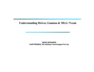
- 1. Understanding Driver, Gamma & MLG /Vcom VIKAS DEOARSHI CHIPTRONIKS, VD Intellisys Technologies Pvt Ltd
- 2. Panel Block Diagram DC/DC Converter Source driver IC InterfaceConnector TTL / RSDS / Mini-LVDS VDD Gamma Data&Clk STH, CPH TP1,POL Von, Voff AVDD, DVDD Gamma Ref. DVDD Panel Block Diagram (c) CHIPTRONIKS , VD Intellisys Technologies pvt ltd 2 Timing Controller Gate Driver IC InterfaceConnector Data, Clk &Control TTL/TMDS / LVDS LC Cs Vcom Vcom STV,CPV Von, Voff DVDD DVDD
- 3. 1. Driver IC Technology (c) CHIPTRONIKS , VD Intellisys Technologies pvt ltd 3
- 4. Source DI &Gate DI Principium Inversion method Driver IC Technology 1. Driver IC Technology (c) CHIPTRONIKS , VD Intellisys Technologies pvt ltd 4 Inversion method Charge Sharing Offset Cancellation
- 5. Source (Data) Driver -Accepts video data and delivers it to the data lines Gate Driver TFT LCD Parts Function 1. Driver IC Technology (c) CHIPTRONIKS , VD Intellisys Technologies pvt ltd 5 Gate Driver -Control TFT on/off
- 6. T-CON Data Load SD1 … SD2 … SD3 … SD8 … … 1 384 385 768 769 1152 2689 30722 … … … …Start VerticalStart TFT-LCD Module drive structure diagram 1. Driver IC Technology (c) CHIPTRONIKS , VD Intellisys Technologies pvt ltd 6 1 384 385 768 769 1152 2689 3072 1R 128B 129R 256B 257R 384B 897R 1024B 2 1G XGA LCD Panel (1024 x RGB x 768) GD1 GD2 GD3 VerticalStart 1 768 257
- 7. LVCKP/N Tx + - Rx (RSDS Mini-LVDS) LVR1P/N LVG1P/N LVB1P/N LVR2P/N LVG2P/N LVB2P/N R1/G1/B1/R2/G2/B2 TP1 SCLK Shift Registers First Line Latches Second Line Latches … … … 1 2 80 1. Driver IC Technology (c) CHIPTRONIKS , VD Intellisys Technologies pvt ltd 7 Source DI Structure Level Shifters DAC … … VREF Output Buffers … 1 2 3 4 480 T-CON POL
- 8. Input Level Shifter & Control Logic DIO2 DIO1 LR CPV Shift Registers Level Shifters … 1. Driver IC Technology (c) CHIPTRONIKS , VD Intellisys Technologies pvt ltd 8 Gate DI Structure … Output Buffers … 1 2 3 4 256 VGH VDD VSS VGL Input & DIO LCD Driving Outputs Internal Logic
- 9. Frame Inversion Inversion Main Category 1. Driver IC Technology (c) CHIPTRONIKS , VD Intellisys Technologies pvt ltd 9 Line Inversion Dot Inversion
- 10. G1 G2 G3 S1 2 2 2 2 2 2 2 2 2 Frame Inversion In order to prevent the aging of liquid crystal materials, liquid crystal molecules at both ends of the voltage is not allowed to have a DC component 。 1. Driver IC Technology (c) CHIPTRONIKS , VD Intellisys Technologies pvt ltd 10 S2 S3 S4 (+) Field Frame (-) Field Frame (+) Field Frame 1 2 3 1 2 3 1 2 3 3 2 1 3 2 1 3 2 1 2 0 2 2 0 2 2 0 2 Frame Inversion
- 11. Line Inversion The voltage polarity of the common electrode is modulated The source driver is driven at low voltage G1 G2 G3 S1 2 2 2 2 2 2 2 2 2 Vcom 1. Driver IC Technology (c) CHIPTRONIKS , VD Intellisys Technologies pvt ltd 11 Line Inversion S2 S3 S4 (+) Field Frame (-) Field Frame (+) Field Frame 1 2 3 1 2 3 1 2 3 3 2 1 3 2 1 3 2 1 2 0 2 2 0 2 2 0 2
- 12. G1 G2 G3 S1 2 2 2 2 2 2 2 2 2 Dot Inversion 1. Driver IC Technology (c) CHIPTRONIKS , VD Intellisys Technologies pvt ltd 12 S2 S3 S4 (+) Field Frame (-) Field Frame (+) Field Frame 1 2 3 1 2 3 1 2 3 3 2 1 3 2 1 3 2 1 2 0 2 2 0 2 2 0 2 Dot Inversion
- 13. There will be more or less offset (voltage drift) on the op amp of the Source Driver IC. And offset will make the output voltage deviation from the original target voltage, resulting in the output voltage is not correct. Offset Cancellation Offset Cancellation 1. Driver IC Technology (c) CHIPTRONIKS , VD Intellisys Technologies pvt ltd 13 output voltage deviation from the original target voltage, resulting in the output voltage is not correct. In order to reduce the occurrence of offset, in addition to the circuit design to minimize the occurrence of offset, is to find ways to compensate for offset, so that the output voltage can be compensated back to become the correct voltage.
- 14. TP POL 1. Driver IC Technology (c) CHIPTRONIKS , VD Intellisys Technologies pvt ltd 14 Odd Outputs Even Outputs Vcom V6 ~V10 V1 ~V5 V6 ~V10 V1 ~V5
- 15. 1. Driver IC Technology (c) CHIPTRONIKS , VD Intellisys Technologies pvt ltd 15 Offset Cancellation Diagram
- 16. Charge Sharing 1. Driver IC Technology (c) CHIPTRONIKS , VD Intellisys Technologies pvt ltd 16
- 17. A A T Positive Drive A/2 A/2 Positive Drive 1. Driver IC Technology (c) CHIPTRONIKS , VD Intellisys Technologies pvt ltd 17 Negative Drive A No Charge Sharing P=A2*C/T*N N : Number of Channel C : Panel Load Negative Drive Charge Sharing P=A2/4*C/T*N Low Power Consumption of Charge Sharing
- 18. 2. MLG Circuit Understanding (c) CHIPTRONIKS , VD Intellisys Technologies pvt ltd 18
- 19. MLG Circuit 2. MLG Circuit Vgh △Vp Cgs ΔVp = X ΔVg Clc + Cst + Cgs (c) CHIPTRONIKS , VD Intellisys Technologies pvt ltd 19 Vcom Vdata Vgl ΔVp production
- 20. MLG Circuit - MLG: Multi level gate,2 level of Vgh. Von Output MLG_H 2. MLG Circuit (c) CHIPTRONIKS , VD Intellisys Technologies pvt ltd 20 MLG_L GND OE2 (from TCON) 3.3V
- 21. Vgh2 1H t2 t3 Vcom Vgh1 2. MLG Circuit (c) CHIPTRONIKS , VD Intellisys Technologies pvt ltd 21 Vcom Vdata Vgl Since the VGH_L, the TFT has not been turned off. At this time in the t3 interval Recharging, can be reduced ΔVp effect
- 22. OE2 - + MLG 2. MLG AVDD (c) CHIPTRONIKS , VD Intellisys Technologies pvt ltd 22 - OE2 as input, resulting in reverse amplification of MLG Output. - The MLG output waveform is input to the Gate Driver IC VGH pin. OE2 MLG_L
- 23. OE2 MLG MLG 2. MLG Circuit (c) CHIPTRONIKS , VD Intellisys Technologies pvt ltd 23 MLG Gate output MLG Waveform
- 24. 3. GAMMA & Vcom Circuit Understanding (c) CHIPTRONIKS , VD Intellisys Technologies pvt ltd 24
- 25. Gamma Correction 3. Gamma & Vcom (c) CHIPTRONIKS , VD Intellisys Technologies pvt ltd 25 N = 2n(R) X 2n(G) X 2n(B) = 23n n : Number of digits of digital data(bit) N : The number of colors that can be displayed 1) R, G, B three primary colors to form a variety of colors 。 2) The number of colors that can be displayed is determined by t he number of bits of the RGB digital signal 。
- 26. Transmittance % 3. Gamma & Vcom (c) CHIPTRONIKS , VD Intellisys Technologies pvt ltd 26 The human viewing angle characteristic is that although the brightness difference on the dark picture is easier to distinguish, But the difference between the brightness of the bright screen is not easy to distinguish
- 27. V-T curve 40.00% 50.00% 60.00% 70.00% 80.00% 90.00% 100.00% 110.00% Trans.[%] 3. Gamma & Vcom (c) CHIPTRONIKS , VD Intellisys Technologies pvt ltd 27 0.00% 10.00% 20.00% 30.00% 40.00% 0.0 2.0 4.0 6.0 8.0 10.0 12.0 Vdata Common electrode voltage V-T Curve
- 28. GMA1 GMA2 GMA3 GMA4 GMA5 R1 R2 R3 R4 R5-1 R11 R22 VDD VDD R5-2 R0 Through the calculation and adjustment, through the following circuit to g enerate the set voltage, and then to the Driver IC input GMA reference volt age, through The internal resistance network of the Driver generates the voltage of eac h gray scale 。 3. Gamma & Vcom (c) CHIPTRONIKS , VD Intellisys Technologies pvt ltd 28 GMA6 GMA7 GMA8 GMA9 GMA10 R6 R7 R8 R9 R33 R44 R5-2 R10 Gamma Correction Circuit
- 29. Vcom Circuit 3. Gamma & Vcom (c) CHIPTRONIKS , VD Intellisys Technologies pvt ltd 29 -Due to ΔVp, the theoretical difference between the Vcom voltage an d the actual Vcom voltage applied is necessary - it is necessary to m inimize Flicker to adjust Vcom.。
- 30. 3. Gamma & Vcom - + Vcom VDD (c) CHIPTRONIKS , VD Intellisys Technologies pvt ltd 30 Vcom Circuit Vcom
- 31. (c) CHIPTRONIKS , VD Intellisys Technologies pvt ltd 31